 Open Access Article
Creative Commons Attribution 3.0 Unported Licence
High-resolution imaging with SEM/T-SEM, EDX and SAM as a combined methodical approach for morphological and elemental analyses of single engineered nanoparticles
Steffi
Rades
*a,
Vasile-Dan
Hodoroaba
a,
Tobias
Salge
b,
Thomas
Wirth
a,
M. Pilar
Lobera
c,
Roberto Hanoi
Labrador
d,
Kishore
Natte
ae,
Thomas
Behnke
f,
Thomas
Gross
a and
Wolfgang E. S.
Unger
*a
aBAM Federal Institute for Materials Research and Testing, Division 6.8 Surface Analysis and Interfacial Chemistry, Unter den Eichen 44-46, 12203 Berlin, Germany. E-mail: wolfgang.unger@bam.de; Fax: +49 30 8104 1829; Tel: +49 30 8104 1823
bBruker Nano GmbH, Am Studio 2D, 12489 Berlin, Germany
cNanoscience Institute of Aragon (INA)-University of Zaragoza; and Networking Research Centre for Bioengineering, Biomaterials and Nanomedicine (CIBER-BBN), Edif. I+D, Campus Río Ebro, C/Mariano Esquillor s/n, E-50018 Zaragoza, Spain
dNanologica AB, Drottning Kristinas Väg 61, SE 11428, Stockholm, Sweden
eLeibniz-Institut für Katalyse e. V. (LIKAT Rostock), Albert-Einstein-Str. 29 a, 18059 Rostock, Germany
fBAM Federal Institute for Materials Research and Testing, Division 1.10 Biophotonics, Richard-Willstätter-Str. 11, 12489 Berlin, Germany
First published on 7th October 2014
Abstract
The combination of complementary characterization techniques such as SEM (Scanning Electron Microscopy), T-SEM (Scanning Electron Microscopy in Transmission Mode), EDX (Energy Dispersive X-ray Spectroscopy) and SAM (Scanning Auger Microscopy) has been proven to be a powerful and relatively quick characterization strategy for comprehensive morphological and chemical characterization of individual silica and titania nanoparticles. The selected “real life” test materials, silica and titania, are listed in the OECD guidance manual as representative examples because they are often used as commercial nanomaterials. Imaging by high resolution SEM and in the transmission mode by T-SEM allows almost simultaneous surface and in-depth inspection of the same particle using the same instrument. EDX and SAM enable the chemical characterization of bulk and surface of individual nanoparticles. The core–shell properties of silica based materials are addressed as well. Titania nominally coated by silane purchased from an industrial source has been found to be inhomogeneous in terms of chemical composition.
Introduction
Due to the varied applications of nanoparticles in consumer and industrial products, human exposition and release to the environment are essential topics that need to be addressed by the OECD sponsorship program and regulation bodies, too. Examples for consumer products containing nanoparticles can be found in highly relevant fields, e.g. cosmetics, food and beverages, and clothing. In this context, nanoscaled TiO2 and SiO2 are high-priority and “true-to-life” materials.1,2 However, there is still a lack of standardized toxicological and physico-chemical characterization methods for systematic evaluation and managing the risk of engineered nanoparticles. Under the generic term nano, the differences in particle size, morphology and composition (just to name a few of them) are cached; nevertheless, they influence their (eco)-toxicological properties, and consequently, hazard identification and risk assessment. A fundamental prerequisite for conducting and assessing toxicological studies is to have a sufficiently and comprehensively characterized test material. Parameters to be addressed include particle size distribution, morphology, agglomeration/aggregation state, composition and description of surface chemistry (e.g. coating or modification).3 The OECD has set-up such a list of physico-chemical measurands that should be determined for particles sponsored for toxicity testing.4Powerful complementary characterization techniques capable of analyzing morphology, size and chemical composition at the surface and in the bulk of single nanoparticles are analytical electron microscopy, i.e. a combination of Scanning Electron Microscopy (SEM) with Energy Dispersive X-ray Spectroscopy (EDX), and Scanning Auger Microscopy (SAM). These methods are closely related to each other. In all the cases, a finely focused electron beam is scanned across the surface of a sample. When nanoparticles are investigated, a common preparation strategy can be used: dropping of dispersed particles onto a TEM grid. Morphology and shape information are derived from the detection of secondary electrons in SEM and, more suited for such purposes, transmitted electrons in T-SEM modes, analytical information from characteristic X-rays (EDX) and Auger electrons (SAM) that are emitted as the result of radiative, and correspondingly, non-radiative decay events of core holes. Core holes are formed by the ionizing interaction of the primary electron beam with atoms constituting the sample. Surface sensitivity is achieved in the SAM analysis because the inelastic mean free path of the Auger electrons is typically <10 nm (e.g. ≅3.1 nm of Si KLL Auger electrons). Bulk information is delivered by EDX with electron excitation because typical X-ray photons may travel across a solid at the micrometer scale.
In contrast to assemble methods such as Small Angle X-ray Scattering (SAXS), Dynamic Light Scattering (DLS), X-ray Photoelectron Spectroscopy (XPS), X-ray Diffraction (XRD) and Brunauer–Emmett–Teller method (BET), SAM and (T-)SEM/EDX are two of the very few methods in nano analytics that have the capability to address individual nanoparticles.
In this report, we will present a number of case studies undertaken by complementary (T-)SEM/EDX/SAM analysis of different test materials. One such class is silica in its non-porous as well as its mesoporous forms. The core–shell properties of silica based materials5 are addressed as well. Another test material is titania, which has been purchased from an industrial source as silane coated nanoparticles. Both “true-to-life” test materials under investigation—silica and titania—are listed in the OECD guidance manual.4 These case studies are presented as the applications of the proposed combined analytical approach, which enables the routine morphological and chemical characterisations of individual nanoparticles in heterogenous batches originating from industrial processes. Moreover, heterogenous samples collected at work spaces and in the environment will be another area of application in the near future.
As far as we know, the combination of complementary SEM/T-SEM/EDX/SAM analysis has not been exploited on nanoscaled silica and titania yet. Here, we present the analysis of single- and multi-component nano-objects such as nanoparticles and core–shell systems by resolving their internal/external structure not only by imaging but in combination with chemical analysis.
Experimental
Materials, synthesis and pre-characterization
The physico-chemical pre-characterization of mesoporous nano-scaled silica has been carried out by ensemble methods such as BET, XPS and XRD to determine the size of mesopores, chemical composition and structure. Furthermore, to examine individual particles, TEM was employed in order to measure the particle size distribution and mesoporosity. These pre-examinations act as an independent control of the results obtained by the T-SEM, EDX and AES methods, which will be the focus of this report.
The nitrogen gas adsorption analysis was performed in a Micromeritics TriStar 3000 system. Before the analysis, the sample was placed in the sample holder and was heated to 423 K at a rate of 10 K min−1 while degassing down to 10−5 bar for 180 min. The sample mass after degassing was 0.2508 g with the initial mass being 0.2616 g. The sample was subsequently transferred to the analysis port of the device and subjected to the measuring protocol that comprises further degassing for 180 min, free-volume determination using He gas at both room temperature (298 K) and cold (77 K) conditions, and finally, analysis at 77 K. The relative pressures and adsorbed gas volumes were automatically determined using the built-in analysis routines of the TriStar device.
Nitrogen adsorption and desorption isotherms have been measured for the NNV-001 silica nanoparticles at 77 K. According to the IUPAC classification, the isotherm is identified to be of type IV, which is commonly assigned to mesoporous materials with low or negligible microporous volumes.6 Moreover, the shape of the isotherm is similar to that found for ordered mesoporous materials such as those of the family M41S.7,8 The values of the specific surface area SBET and of the pore volume Vp of the material are 949 m2 g−1 and 0.48 cm3 g−1, respectively, which are determined by applying the BET procedure. Furthermore, the estimation of the mesoporous size DP was calculated to be 2.0 nm by applying the Barrett–Joyner–Halenda (BJH) approximation to the adsorption branch of the isotherm.
XPS measurements were carried out with an AXIS Ultra DLD electron spectrometer manufactured by Kratos Analytical, UK. The XPS spectra were recorded using monochromatized Al Kα excitation at a pass energy of 80 eV for survey spectra and 20 eV for the core level spectra. The electron emission angle was 0° and the source-to-analyzer angle was 60°. The binding energy scale of the instrument was calibrated following the Kratos Analytical procedure that uses ISO 15472 binding energy data.9 The spectra were taken by setting the instrument to the hybrid lens mode and the slot mode providing approximately a 300 × 700 μm2 analysis area. A charge neutralizer was used. The binding energy scale was corrected for charging10 using an electron binding energy of 285.0 eV (ref. 11) for the C1s binding energy of aliphatic hydrocarbons. This correction procedure may be an additional source of uncertainty of the binding energy. The spectra have been analyzed with the program CasaXPS versions 2.3.15 and 2.3.16.12 The NNV-001 sample has been prepared for measurement on a double sided adhesive tape (Scotch™).
In the XPS spectra of NNV-001, only the elements Si, O and C have been identified. On the surface of NNV-001, carbon occurs at low surface concentrations due to the adsorbed hydrocarbons originating from ambient air exposure. The quantification results of the test material are displayed in Table 1. The O/Si atomic ratio (≅2.4) is higher than the theoretical value. This could be due to some oxygenated groups present in the hydrocarbon adsorption layer. The binding energies measured for Si2p and O1s are very close to the reference values published in the literature for silica.
| Peak | Binding energy/eV | Surface concentration/at.% |
|---|---|---|
| O1s | 533.3 | 68 |
| C1s | 285.0 | 4 |
| Si2p | 103.9 | 28 |
The silica material was characterized by X-ray diffraction (XRD) at room temperature on a D-Max Rigaku diffractometer with a rotating anode, operating at 40 kV and 80 mA. The set-up is equipped with a copper anode and a graphite monochromator to select CuKα radiation (2theta = 10–90°; the diffractogram was scanned using 0.03° steps and a counting time of 1 s per step).
The XRD pattern of the silica particles does not exhibit a regular pattern, and only a broad band emerges at about 2theta = 24°. This indicates that the silica particles synthesized by Nanologica AB have the typical structure of amorphous silica.
TEM instrumentation and sample preparation
Mesoporous nano-scaled silica (NNV-001) has been characterized by Transmission Electron Microscopy (TEM) in a FEI Tecnai T20 microscope using copper grids as the sample holder. TEM Imaging and Analysis software (TIA) was used for TEM image processing.The sample suspension (concentration: 10 ppm) was sonicated for 1 min in a bath to ensure a well-dispersed suspension. Then, a drop (5–20 μL) of the suspension was deposited on the TEM grid and allowed to dry for at least 24 h at room temperature.
SEM/T-SEM/EDX instrumentation and sample preparation
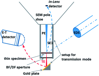
The SEM Zeiss Supra 40 utilized here is equipped with a high-resolution cathode (Schottky field emitter) and an In-Lens SE (secondary electrons) detector used in the high resolution mode, which significantly enhances the quality of the images of nanoparticles when compared to those obtained by a conventional Everhart–Thornley (E–T) detector. Furthermore, the SEM can be operated in the transmission mode, i.e. the so-called T-SEM (Transmission in Scanning Electron Microscope) (see Fig. 1). In the transmission mode, advanced nanoparticle analysis can be accomplished by gaining in-depth information as well as very accurate lateral information, e.g., for size distribution analysis of ensembles of nanoparticles. The so-called STEM (Scanning Transmission Electron Microscopy) detector is often used for performing transmission imaging in a SEM instrument.13 Instead of this, we used the so-called single-unit transmission set-up as commercially available from Zeiss14,15 (see Fig. 1). Both sample and substrate (e.g. a TEM grid) have to be electron transparent at electron energies ≤30 keV, which is the typical range for SEM. This transmission unit holds the sample, which is usually prepared on a conventional TEM grid with a thin foil as the substrate. Primary electrons transmitted by the sample impinge on a gold plate under the bright/dark field aperture. The role of the gold plate is to converse and multiply the transmitted electrons into secondary electrons, which are then collected by the conventional Everhart–Thornley detector. The direct way of the secondary electrons emitted by the sample surface towards the E–T detector is blocked by a dedicated screening ring. More information on the operation of the setup can be found in other papers.16,17 The combination of the two techniques, In-Lens detection and T-SEM, enables the high-resolution top-surface and in-depth observation of nanoparticles.18 In addition to imaging the sample surface morphology and structure, elemental analysis can be conducted with an EDS (Energy Dispersive X-ray Spectrometer) detector. EDX spectra were measured with a Si(Li) EDS detector (Thermo Scientific) or an XFlash® SDD detector (Bruker), both having an active area of 10 mm2. For one particular case study, a large-area SDD EDS detector (Bruker) capable of high-sensitivity detection has been used.The outlined approach enables a comprehensive analysis of nanoparticles in terms of size, shape and morphology, as well as elemental composition.
The samples have been prepared for analysis by using a few microliters of the sample solution, which is dropped onto conventional TEM grids. Most often, TEM copper grids coated with a carbon foil (Plano) have been used. The grid with the droplet was dried in air. It should be noted that particles have to be sufficiently dispersed on the grid. Otherwise, for EDX imaging, X-ray signals coming from different particles could overlap due to cross excitation, and therefore, it is recommended to measure with EDX on isolated particles.
AES instrumentation and sample preparation
A PHI 700 Auger Scanning Probe (ULVAC-PHI Inc.) equipped with a coaxial cylindrical mirror analyzer (CMA) was used in SEM and Scanning Auger Microscopy modes. Auger electrons were excited by primary electron beams of 20 kV @ 1 nA and 25 kV @ 1 nA. The primary electron beam impinges on the surface at normal incidence. Measurements started with imaging nanoparticles by secondary electrons (SEM mode) in order to re-localize the points of interest. These particles were investigated by spectral point analysis, line scans and element mapping.Sample preparation procedures were taken over one-by-one from the T-SEM experiments.
Results and discussion
Case study I: characterization of mesoporous silica particles
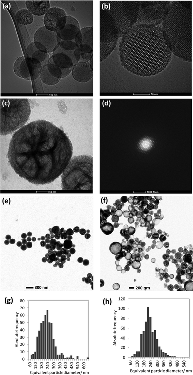
Silica with mesoporosity is characterized by a very high (and variable) surface area, differentiated in the outer and inner pore surface, high and tunable pore volume, adjustable pore size, pore network of various types and structures (controllable nanoparticle size) combined with silanol groups for functionalization in the outer and inner surfaces.19–28 Structurally, nanoporous silica particles reveal porous order on the mesoscopic scale and disorder on the atomic scale.7 The channels, cages or pores, formed within the materials are supported by an amorphous silica wall and are arranged periodically on a lattice. Nanoporous silica has become, in the last decade, a popular matrix for the incorporation and support of functional species. The resulting advantages and potential applications based thereof include loading, transport and release of drugs. Based on the adsorption of active molecules besides pharmaceutical drugs,20,29,30 fat soluble vitamins31 and flavors32,33 onto stable, non-erosive nano (meso-) porous materials have been explored.34The particle size analysis of the as-prepared dispersion has been done by using T-SEM (see representative particles in Fig. 2e), revealing the poly-disperse characteristic of NNV-001. The mean of the area equivalent particle diameters and ± one standard deviation of the particle size distribution (written in the brackets) were around 230 (90) nm (Fig. 2g). AES and EDX measurements were done with fresh and stored dispersions. For particle size verification, analysis was re-done with these aged dispersions. There has been no significant change of the mean value of the equivalent particle diameter (230 (70) nm). The size distribution of a representative number of particles imaged in Fig. 2f is displayed in Fig. 2h. There are even a few particles present, much bigger, up to about 1 μm, observed in the T-SEM micrographs, but not shown in the size distributions in Fig. 2g and h. Additional information on the capability of T-SEM to accurately measure nanoparticle size distribution is extensively reported in Buhr et al.35,36
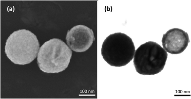
Using the In-Lens detector for high resolution SEM, individual silica NNV-001 nanoparticles were imaged (Fig. 3a). They are rather spherical with a rough surface. T-SEM images in bright-field (BF) mode reveal specific differences for those three nanoparticles displayed in Fig. 3a by exploitation of the transmission image contrast as shown in Fig. 3b. Herein, the contrast is more sensitive to local differences in the sample density/atomic number. The T-SEM imaging mode allows a classification of the silica NNV-001 particles as follows:
•The first class consists of crystalline nanoparticles having ordered mesopores. They show a dark image contrast in the BF transmission mode (see left particle in Fig. 3b) and appear to be homogeneous.
•The second class is constituted of nanoparticles having non-aligned mesopores (middle particle in Fig. 3b and particle as shown in Fig. 2c).
•Particles belonging to the third class appear as “core–shell” systems in the T-SEM image (right particle in Fig. 3b). Actually, they seem to be hollow.
Note that the high-resolution, surface-sensitive imaging mode used for In-Lens SEM (cf.Fig. 3a) is not sufficient to distinguish the three classes of silica particles constituting the silica NNV-001 batch, because differentiation is only possible by the analysis of the inner structures. Similar porous and hollow silica nanoparticles have been recently investigated by Teng et al.,37 which is based on conventional TEM image data. The conclusion is that the silica NNV-001 particles are not uniform. This inhomogeneity might be ascribed to the sample preparation procedure, which consists of dispersion in water. Teng et al.37 investigated the changes of the structure of mesoporous silica nanoparticles depending on the experimental conditions. They showed that the longer and higher the temperature of incubated silica spheres in water is, the more the transformations of mesostructured silica spheres into hollow spheres are. In the investigated silica NNV-001 sample, we obviously observe different stages of this solid-to-hollow transformation, all co-existing in the same batch.
•These mesoporous silica particles that are crystalline and the ordered pores therein exhibit EDX Si Kα and O Kα intensity line scans with a “single mountain” profile (see Fig. 4a). This line scan correlates to the rather uniform material contrast obtained in T-SEM.
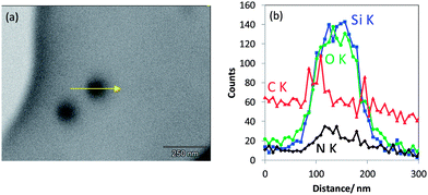
•Particles with non-ordered mesopores and showing “crushed” surface in In-Lens SEM (middle particle in Fig. 3a) belong to the second class of particles mentioned above. They are characterised by top-hat shaped line scan profiles for both Si Kα and O Kα, as displayed in Fig. 4b, which are different from those obtained with crystalline mesoporous silica particles. The difference in the line scan shape of the two classes of silica nanoparticles originates obviously from the differences in the local particle density corresponding to silica with aligned and non-aligned mesoporous structure.
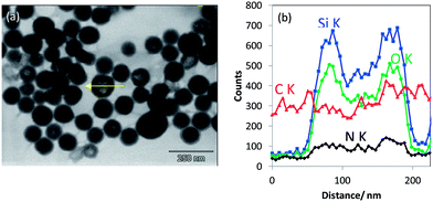
•The line scan profiles in Fig. 4c are, with their two maxima structures, typical for hollow silica nanoparticles (belonging to the “third class” as defined above).
In addition to the particular line scan intensity distributions displayed in Fig. 4, one other interesting finding is that the stoichiometry—represented by the Si Kα to O Kα intensity ratio—of all the three classes of silica nanoparticles is almost the same, considering the level of noise. The results for a rather seldom class of nano scaled silica particles are shown in Fig. 5. These particles are homogeneous in image contrast (cf.Fig. 5a) and the EDX O Kα and Si Kα line intensities of the line scan are represented in Fig. 5b. It is striking that there is a strongly enhanced Si Kα signal when compared to the O Kα signal and to the line scan displayed earlier in Fig. 4 measured under the same experimental conditions. This indicates that this particle has an elemental composition that differs significantly (more silicon and less oxygen) from that of all the silica particles discussed before (see Fig. 4a–c).
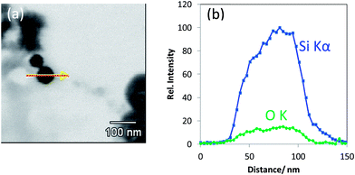 | ||
| Fig. 5 (a) T-SEM image of a silica nanoparticle (d ≅ 65 nm) with an arrow indicating the EDX line scan position and (b) EDX line scan with Si Kα signal and O Kα signal of the particle shown in (a). | ||
Of course, it would be worthwhile to quantify the measured EDX intensities into elemental concentrations. The existing state-of-the-art EDX quantification algorithms are such that they are fairly accurate; however, they are applicable for bulk samples having a homogeneous elemental composition and a flat surface in the range of the interaction volume of the primary electron beam (with energies up to 30 keV in a conventional SEM) with the sample. In dependence on the beam energy as well as the atomic number of the sample constituents, typically, volume in the range of roughly one cubic micrometer can be addressed. This limits the spatial resolution of SEM/EDX. By operating the transmission approach using electron-transparent samples, these prerequisites for an accurate quantification by the existing EDX quantification algorithms are no longer fulfilled. For electron-transparent, thin film samples (lamellae), there are TEM/EDX quantification approaches, which often yield acceptable results. However, such procedures have not been validated yet for the much lower beam voltages used for SEM/EDX working in the transmission mode. Moreover, the so-called k-factor (or Cliff–Lorimer) quantification approaches38,39—applicable to thin layers—have not been tested on (nano)particles. Systematic efforts must be spent in order to develop new and suitable quantitative concepts.40 Another empirical quantification approach would be to directly compare the elemental intensity ratios of the reference materials of similar concentration and size distribution as the particles to be investigated. The main drawback here is constituted by the lack of silica nanoparticle reference materials with valid elemental compositions. On the whole, it remains that the simple comparison of EDX intensity ratios between (nano)particles measured under the same conditions yields reliable semi-quantitative information (although it is not fully satisfying) when performing EDX using SEM in the transmission mode.
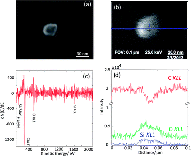
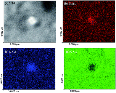
As the next exercise, it has been tried to acquire SAM maps of another silica nanoparticle of roughly the same size. Elemental maps are presented in Fig. 7 and the corresponding point Auger electron spectrum is shown in Fig. 8. Si and O maps characterize the silica particle's surface, revealing that the entire particle's surface consists of Si and O. The carbon map supports the interpretation of the carbon line scan displayed in Fig. 6d. The nanoparticle occurs as a shadow on the carbon film on the TEM grid, and the remaining intensity in the shadow may represent the C surface concentration at the silica nanoparticle. The AES point spectrum taken from the center of the particle's surface with a rather narrow primary electron beam (Fig. 8) reveals the presence of C, O and Si on the surface. Regarding carbon, the C-map in combination with the point spectrum suggests the presence of a carbon coating as contamination of the entire particle surface.
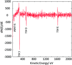 | ||
| Fig. 8 Auger point spectrum (applied beam energy of 20 keV) measured at the center of the silica nanoparticle imaged in Fig. 7. | ||
Case study 2: core–shell character of silica and titania particles
In case of a silica IPTES core–shell particle obviously showing a vesicular morphology in T-SEM (Fig. 10a), the transmission contrast resembles the local mass density (and/or atomic number) of the sample. This is clearly seen by comparison to the significantly enhanced line scan intensities of Si Kα and O Kα in the particle shell region in Fig. 10b. IPTES is the origin of the nitrogen signal. Here, the related high-resolution EDX line scan confirms the vesicular structure of the particles of this type.
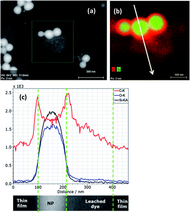
Elemental EDX mapping obtained using a high-sensitivity SDD EDS detector is shown in Fig. 11. The main constituents, namely, C, O and Si, of the core–shell, non-porous silica nanoparticles were successfully detected and signals were used for line scans and imaging. The rather generic EDX signal of C Kα can be used to confirm the existence of an organic layer on the silica nanoparticles. Even with the carbon foil as a substrate, where the particles are deposited upon, the C Kα signal emitted from the particles themselves can be effectively distinguished. A thin carbon-rich shell—in the range of about 10 nm thickness—is detected by the high-sensitivity EDS detector and clearly visualized by extracting a line scan across a particle (white arrow) out from the EDX map in Fig. 11b. Moreover, the line scan shows also that there is carbon-rich material close to the particle. This material is displayed as the reddish region “below” the particles in Fig. 11b. Obviously, dye material from the shell of the particles has leached onto the substrate very likely during sample preparation. One feasibility check allowing this qualitative discussion is the stable intensity of the carbon signal along the EDX line scan in Fig. 11c, which does not change with the time of irradiation. Sample contamination due to carbon cracking at the area of impact of the electron beam on the sample (the thin film substrate, in this case) is well known in electron microscopy. This phenomenon regularly results in a continuous increase of the carbon signal in a line scan vs. time of irradiation plot. Furthermore, very weak signal intensities in the range of the detection limit of the elements N and S have been measured within the particle areas. Both elements are presumably constituents of the dye, and nitrogen is also present in the applied silane coupling agent IPTES. It must be noted that the findings above were possible only by using a high-sensitivity detector with a very large active area (and correspondingly large collection solid angle). A conventional 10 mm2 EDS detector does not provide sufficiently high sensitivity and cannot be used to distinguish the local features as described here. The recent development of large-area EDS detectors is impressive, so that successively larger X-ray fluxes emitted by such tiny samples can be collected through large solid angles. This development will substantially increase the measurement capabilities of the EDX/T-SEM tool in the characterization of nanoparticles.
Conclusions
Imaging by high resolution SEM and the special set-up for transmission (T-SEM) allows almost simultaneously inspecting the same (nano)particle on a short time scale to gain access to the particle's surface and in-depth information. Yet, the T-SEM lateral resolution is limited to particle sizes of about 5–10 nm strongly depending on the type of material. Of course, TEM is superior in imaging performance, but SEM/T-SEM imaging in combination with EDX is a quick and practical tool for nanoanalysis by morphology including size and elemental composition. Current advanced EDS detector systems, e.g. large-area SDD detectors, are further improving the sensitivity necessary for nanoparticle characterization. As a complementary technique, AES has been employed to enable the analysis of the surface of nanoparticles after bulk examination by EDX.For mesoporous silica nanoparticles, In-Lens SEM and T-SEM delivered morphological information confirmed by TEM. Based on these morphological data, the material can be considered as inhomogeneous. There are three coexisting classes: (1) particles with long-range alignment of pores, (2) particles with non-ordered mesopores, and (3) hollow particles. EDX chemical analysis of these particles can be used to differentiate classes (1) and (3), at least. Surface chemical analysis by SAM revealed, besides Si and O, a very thin surface layer of carbonaceous material that may originate from hydrocarbons adsorbed during sample handling on ambient air.
Non-porous silica nanoparticles having a shell of IPTES were analyzed in order to test the combined approach for validation of their core–shell characteristic. Strong indications for the existence of a shell have been derived from the EDX carbon line scans.
EDX elemental mappings of fluorescent silica core–shell nanoparticles, produced from the IPTES functionalized ones by the coupling of Alexa dye®, have been carried out. Here, elemental mappings obtained using a high-sensitivity EDS detector reveal carbon signals well correlated to the Si and O signals representing nanoparticles that are provided with a carbon-rich, i.e. organic, shell.
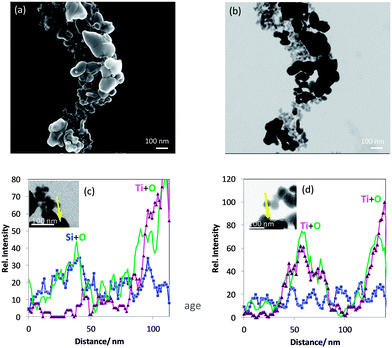
The analysis of the titania–silane nanoparticulate material revealed that it is different from the product label rutile coated with silane. SEM/T-SEM together with different EDX line scans of Ti, Si and O are used to identify at least two kinds of particles as constituents of the material: one kind of particle mainly consists of Si and O and the other one, Ti and O with some minor Si signals. The latter kind could be representative of the rutile coated with silane as specified by the manufacturer.
The combination of complementary characterization techniques such as SEM, T-SEM, EDX and SAM has been proven to be a powerful strategy for comprehensive morphological and chemical characterizations of individual “real life” silica and titania nanoparticles. The case studies facilitate the analysis of multi-elemental nanosystems with complex geometric structures. AES and EDX methods can complement each other and enable to differentiate the elements present in the uppermost surface as well as in-depth and even the whole nanoparticle volume depending on the particle size. The procedures of automatic measurement as well as the evaluation of nanoparticles size, shape and chemical composition by means of both basic techniques (T-SEM/EDX and SAM) are just being developed and tested on real-life products and samples collected from the work space or environment. It is expected by the authors that such promising automatic procedures will be able to be implemented on a routine basis on a statistically relevant number of nanoparticles in the near future, so that the nanoparticle characterization with this combined methodical approach can become significantly efficient.
Acknowledgements
We acknowledge the help of S. Benemann for operating the SEM. The research leading to these results has received funding from the European Union Seventh Framework Programme (FP7/2007-2013) under grant agreement no. 263147 (NanoValid – Development of reference methods for hazard identification, risk assessment and LCA of engineered nanomaterials, see http://www.nanovalid.eu/).References
- A. Narayanan, P. Sharma and B. M. Moudgil, KONA Powder Part. J., 2013, 30, 221 CrossRef CAS.
- G. Orts-gil, K. Natte and W. Österle, RSC Adv., 2013, 3, 18202 RSC.
- A. E. Garcia-Bennett, Nanomedicine, 2011, 6, 867 CrossRef CAS PubMed.
- Guidance Manual for the Testing of Manufactured Nanomaterials: OECD Sponsorship Programme: First Revision. no. 25-ENV/JM/MONO(2009)20/REV.
- K. Natte, T. Behnke, G. Orts-Gil, C. Würth, J. F. Friedrich, W. Österle and U. Resch-Genger, J. Nanopart. Res., 2012, 14, 680 CrossRef.
- K. Sing, D. Everett, R. Haul, L. Moscou, R. Pierotti, J. Rouquerol and T. Siemieniewska, Pure Appl. Chem., 1985, 57, 603 CrossRef CAS.
- C. T. Kresge, M. E. Leonowicz, W. J. Roth, J. C. Vartuli and J. S. Beck, Nature, 1992, 359, 710 CrossRef CAS.
- J. Beck, J. Vartuli, W. Roth, M. Leonowicz, C. Kresge, K. Schmitt, C. Chu, D. Olson and E. Sheppard, J. Am. Chem. Soc., 1992, 114, 10834 CrossRef CAS.
- ISO 15472:2010, Surface chemical analysis – X-ray photoelectron spectrometers – calibration of energy scales.
- ISO 19318:2004, Surface chemical analysis – X-ray photoelectron spectroscopy – reporting of methods used for charge control and charge correction.
- G. Beamson and D. Briggs, High Resolution XPS of Organic Polymers, 1992, p. 26 Search PubMed.
- CasaXPS, http://www.casaxps.com/, 2013.
- J. P. Vermeulen and H. Jaksch, Im. Microsc., 2005, 1, 22 Search PubMed.
- U. Golla and B. Schindler, US Pat., 6 815 678 B2, 2004.
- V.-D. Hodoroaba, S. Benemann, C. Motzkus, T. Macé, P. Palmas and S. Vaslin-Reimann, Microsc. Microanal., 2012, 18(2), 1750 CrossRef.
- V.-D. Hodoroaba, C. Motzkus, T. Macé and S. Vaslin-Reimann, Microsc. Microanal., 2014, 20, 602 CrossRef CAS PubMed.
- V.-D. Hodoroaba, D. Akcakayiran, D. O. Grigoriev and D. G. Shchukin, Analyst, 2014, 139, 2004 RSC.
- V.-D. Hodoroaba, S. Rades and W. Unger, Surf. Interface Anal., 2014 DOI:10.1002/sia.5426.
- H. Yamada, C. Urata, Y. Aoyama, S. Osada, Y. Yamauchi and K. Kuroda, Chem. Mater., 2012, 24, 1462 CrossRef CAS.
- M. Vallet-Regi, F. Balas and D. Arcos, Angew. Chem., Int. Ed., 2007, 46, 7548 CrossRef CAS PubMed.
- K. Ma, H. Sai and U. Wiesner, J. Am. Chem. Soc., 2012, 134, 13180 CrossRef CAS PubMed.
- M. Guo, X. Zou, H. Ren, F. Muhammad, C. Huang, S. Qiu and G. Zhu, Microporous Mesoporous Mater., 2011, 142, 194 CrossRef CAS.
- F. Kleitz, S. H. Choi and R. Ryoo, Chem. Commun., 2003, 2136 RSC.
- H.-K. Na, M.-H. Kim, K. Park, S.-R. Ryoo, K. E. Lee, H. Jeon, R. Ryoo, C. Hyeon and D.-H. Min, Small, 2012, 8, 1752 CrossRef CAS PubMed.
- M. Yu, L. Zhou, J. Zhang, P. Yuan, P. Thorn, W. Gu and C. Yu, J. Colloid Interface Sci., 2012, 376, 67 CrossRef CAS PubMed.
- S. Huh, J. W. Wiench, J.-C. Yoo, M. Pruski and V. S.-Y. Lin, Chem. Mater., 2003, 15, 4247 CrossRef CAS.
- S. Che, S. Lim, M. Kaneda, H. Yoshitake, O. Terasaki and T. Tatsumi, J. Am. Chem. Soc., 2002, 124, 13962 CrossRef CAS PubMed.
- J. Zhang, M. Liu, A. Zhang, K. Lin, C. Song and X. Guo, Solid State Sci., 2010, 12, 267 CrossRef CAS.
- X. Xia, C. Zhou, L. Ballell and A. E. Garcia-Bennett, ChemMedChem, 2012, 7, 43 CrossRef CAS PubMed.
- M. Stromme, U. Brohede, R. Atluri and A. E. Garcia-Bennett, WIREs Nanomed. Nanobiotechnol., 2009, 1, 140 CrossRef CAS PubMed.
- C. Zhou, X. Xia and A. E. Garcia-Bennett, Super-saturating delivery vehicles for poorly water soluble pharmaceutical and cosmetic ingredients, PCT/EP2011/065959, 2011 Search PubMed.
- Ordered porous silica particles for encapsulation of food ingredients and nutraceuticals and encapsulation, patent in submission.
- R. Corkery, A. Feiler, J. A. Grover, C. Dimelow and E. George, Anti-caking agent for flavored products, PCT/US2011/028108, 2011 Search PubMed.
- B. Fadeel and A. E. Garcia-Bennett, Adv. Drug Delivery Rev., 2010, 62, 362 CrossRef CAS PubMed.
- E. Buhr, N. Senftleben, T. Klein, D. Bergmann, D. Gnieser, C. G. Frase and H. Bosse, Meas. Sci. Technol., 2009, 20, 084025 CrossRef.
- C. Motzkus, T. Macé, F. Gaie-Levrel, S. Ducourtieux, A. Delvallee, K. Dirscherl, V.-D. Hodoroaba, I. Popov, O. Popov, I. Kuselman, K. Takahata, K. Ehara, P. Ausset, M. Maillé, N. Michielsen, S. Bondiguel, F. Gensdarmes, L. Morawska, G. R. Johnson, E. M. Faghihi, C. S. Kim, Y. H. Kim, M. C. Chu, J. A. Guardado, A. Salas, G. Capannelli, C. Costa, T. Bostrom, Å. K. Jämting, M. A. Lawn, L. Adlem and S. Vaslin-Reimann, J. Nanopart. Res., 2013, 15, 1919 CrossRef.
- Z. Teng, X. Su, Y. Zheng, J. Sun, G. Chen, C. Tian, J. Wang, H. Li, Y. Zhao and G. Lu, Chem. Mater., 2013, 25, 98–105 CrossRef CAS.
- G. Cliff and G. W. Lorimer, J. Microsc., 1975, 103, 203 CrossRef.
- M. Watanabe and D. B. Williams, J. Microsc., 2006, 221, 89 CrossRef CAS PubMed.
- R. Gauvin, Microsc. Microanal., 2012, 18, 915 CrossRef CAS PubMed.
- S. Rades, T. Wirth and W. Unger, Surf. Interface Anal., 2014 DOI:10.1002/sia.5378.
- Y. Li, S. Mao and Z. Ding, in Monte Carlo Simulation of SEM and SAM images, Applications of Monte Carlo Method in Science and Engineering, ed. S. Mordechai, InTech, 2011, www.intechopen.com Search PubMed.
- H. Ito, M. Ito, Y. Magatani and F. Soeda, Appl. Surf. Sci., 1996, 100/101, 152 CrossRef CAS.
- K. Natte, W. Österle, J. F. Friedrich, R. von Klitzing and G. Orts-Gil, Macromol. Chem. Phys., 2012, 213, 2412 CrossRef CAS.
- K. Natte, J. F. Friedrich, S. Wohlrab, J. Lutzki, R. von Klitzing, W. Österle and G. Orts-Gil, Colloids Surf., B, 2013, 104, 213 CrossRef CAS PubMed.
- G. Orts-Gil, K. Natte, R. Thiermann, M. Girod, S. Rades, H. Kalbe, A. F. Thünemann, M. Maskos and W. Österle, Colloids Surf., B, 2013, 108, 110 CrossRef CAS PubMed.
- V. Ntziachristos, C. Bremer and R. Weissleder, Eur. J. Radiol., 2003, 13(195), 2003 Search PubMed.
- R. Weissleder, Nat. Biotechnol., 2001, 19, 316 CrossRef CAS PubMed.
| This journal is © The Royal Society of Chemistry 2014 |

