
Stable continuous-wave lasing from discrete cesium lead bromide quantum dots embedded in a microcavity†
Hongbo
Zhang‡
a,
Wen
Wen‡
a,
Bowen
Du‡
ad,
Lei
Zhou
 f,
Yu
Chen
ag,
Shun
Feng
ah,
Chenji
Zou
a,
Lishu
Wu
a,
Hong Jin
Fan
a,
Weibo
Gao
a,
Handong
Sun
*a,
Jingzhi
Shang
*e and
Ting
Yu
*bc
f,
Yu
Chen
ag,
Shun
Feng
ah,
Chenji
Zou
a,
Lishu
Wu
a,
Hong Jin
Fan
a,
Weibo
Gao
a,
Handong
Sun
*a,
Jingzhi
Shang
*e and
Ting
Yu
*bc
aDivision of Physics and Applied Physics, School of Physical and Mathematical Sciences, Nanyang Technological University, Singapore 637371, Singapore. E-mail: hdsun@ntu.edu.sg
bSchool of Physics Science and Technology, Wuhan University, Wuhan 430072, People's Republic of China. E-mail: yu.ting@whu.edu.cn
cWuhan Institute of Quantum Technology, Wuhan 430206, China
dCollege of Physics and Optoelectronic Engineering, Shenzhen University, Shenzhen 518060, China
eShaanxi Institute of Flexible Electronics (SIFE), Northwestern Polytechnical University (NPU), Xi’an, 710129, China. E-mail: iamjzshang@nwpu.edu.cn
fSchool of Chemical Engineering and Technology, Sun Yat-Sen University, Zhuhai 519082, PR China
gCommonwealth Scientific and Industrial Research Organisation (CSIRO) Manufacturing, Clayton, Victoria 3168, Australia
hInstitute of Photonics and Quantum Sciences, SUPA, Heriot-Watt University, Edinburgh EH14 4AS, UK
First published on 14th July 2023
Abstract
All-inorganic cesium lead bromide (CsPbBr3) quantum dots (QDs) with high photoluminescence (PL) quantum efficiency have been reported as ideal gain materials for high-performance lasers. Nevertheless, isolated CsPbBr3 QDs have not achieved lasing emission (LE) due to finite absorption cross-section. Here, we demonstrate continuous-wave lasing of isolated CsPbBr3 QDs embedded in a microcavity. Distributed Bragg reflectors (DBRs), together with isolated CsPbBr3 QDs in a polymer matrix, are introduced to construct a vertical-cavity surface-emitting laser (VCSEL), which exhibits stable single-mode lasing emissions with an ultra-low threshold of 8.8 W cm−2 and a high Q factor of 1787. Such perovskite-based microcavity structures sustain highly stable excitons at room temperature and can provide an excellent experimental platform to further study the single-particle nano-lasers and quantum physics frontiers such as exciton–polariton condensation, single-photon emission, and optical quantum communication.
New conceptsWe demonstrate a groundbreaking concept by employing all-inorganic cesium lead bromide (CsPbBr3) quantum dots (QDs) as gain media in a high-Q vertical-cavity surface-emitting laser (VCSEL), overcoming previous limitations of achieving continuous-wave (CW) lasing using lead halide perovskite QDs and enabling stable room temperature operation. This novel approach differentiates itself from existing research by incorporating CsPbBr3 QDs into a high-Q vertical microcavity, leveraging the unique properties of metal halide perovskites for ultra-low-power photoexcitation. Our work brings valuable insights into the materials science domain by providing a cost-effective solution for the development of practical perovskite laser devices, utilizing the facile processability and defect-tolerance of these materials. The outstanding performance and stability of the CsPbBr3-QD VCSEL, including a high-quality factor of 1787, an ultra-low threshold of 8.8 W cm−2, and the ability to maintain lasing characteristics after one year of storage under ambient conditions, exemplify the potential of this concept. Furthermore, this breakthrough lays the foundation for future research on single-particle nano-lasers and quantum physics phenomena, ultimately advancing next-generation optical and quantum technologies. |
Metal halide perovskites are a fantastic family of semiconductors with a basic structure of ABX3 in common, where A is an organic cation like methylammonium (CH3NH3+), formamidinium (NH2CH
![[double bond, length as m-dash]](https://www.rsc.org/images/entities/char_e001.gif) NH2+), or an inorganic cation like cesium (Cs+), B is a metallic cation including lead (Pb2+) and tin (Sn2+), and X represents a halide anion such as iodide (I−), bromide (Br−) and chloride (Cl−).1 Due to their ultralong photocarrier diffusion length, large absorption coefficient, high quantum efficiency, facile solution processability, and defect tolerance,2 metal halide perovskites have emerged as the next-generation light-emitting materials for novel photonic and optoelectronic devices, such as light-emitting diodes (LEDs),3,4 photonic detectors,5 and optical sensors.6 As a direct band gap semiconductor, such excellent performance is benefited from their broadly tunable emission wavelengths, efficient radiative recombination, and strong excitonic effects, which are also widely believed as crucial characteristics for developing practical laser devices.7
NH2+), or an inorganic cation like cesium (Cs+), B is a metallic cation including lead (Pb2+) and tin (Sn2+), and X represents a halide anion such as iodide (I−), bromide (Br−) and chloride (Cl−).1 Due to their ultralong photocarrier diffusion length, large absorption coefficient, high quantum efficiency, facile solution processability, and defect tolerance,2 metal halide perovskites have emerged as the next-generation light-emitting materials for novel photonic and optoelectronic devices, such as light-emitting diodes (LEDs),3,4 photonic detectors,5 and optical sensors.6 As a direct band gap semiconductor, such excellent performance is benefited from their broadly tunable emission wavelengths, efficient radiative recombination, and strong excitonic effects, which are also widely believed as crucial characteristics for developing practical laser devices.7
Recently, great efforts have been devoted to achieving lasing from metal halide perovskites.8 In spite of intensive studies of lasing under pulse excitation conditions, experimental demonstrations and in-depth understandings of continuous-wave (CW) lasing from lead halide perovskites are still challenging,9 especially the devices operating stably at room temperature. Therefore, a CW perovskite laser with the feature of room-temperature operation, environmental stability, and purely single-mode emission is highly desired. Compared with the traditional organic hybrid perovskites,10 all-inorganic CsPbBr3 QDs, which exhibit a near-unity photoluminescence (PL) quantum yield11 and much better stability under the ambient conditions, are the ideal gain material for a high-performance laser.
In this work, we design a VCSEL, where the solution-processed CsPbBr3 QDs are embedded in the cavity as light-emitting active materials. VCSEL is a kind of favored laser because of its capacity to construct planar arrays, high spatial directivity perpendicular to the surface, excellent beam profile, and silicon-based substrate compatibility. Benefiting from a high Q factor of 1787, a single-mode CW lasing emission with an ultra-low threshold of 8.8 W cm−2 was observed at room temperature, which is comprehensively lower than the lasing threshold values reported in the existing perovskite QDs lasers.12 The apparent features of spectral narrowing, nonlinear evolution of the emission intensity, and directional emission manifest the onset of lasing emission. The fabricated CsPbBr3-QD VCSEL exhibits excellent stability, which not only sustains single-mode lasing at room temperature for 300 s under CW optical pumping without degradations, but also reserves its outstanding lasing performance after one-year preservation. This work provides a strategy to design and fabricate planar solution-based perovskite VCSELs toward next-generation coherent light sources.
We synthesized the CsPbBr3 quantum dots (QDs) via a modified hot injection solution method.13 The low-magnification TEM image shows the uniformity of the CsPbBr3 QDs (Fig. 1a). The statistical results of the as-fabricated CsPbBr3 QDs taken from the TEM image are shown in Fig. 1b, where the histogram for the size distribution of the CsPbBr3 QDs is fitted with a normal distribution. The CsPbBr3 QDs show a cubic shape with an average edge length of 9.8 ± 0.97 nm, as shown in Fig. 1c. Besides, the Raman spectrum taken under photoexcitation by a 633 nm CW laser is shown in Fig. 1d, where three peaks are located at 72.8, 127.4, and 310.3 cm−1, respectively. The peak at 72.8 cm−1 is ascribed to the vibrational mode of [PbBr6]4− octahedra, coincident with the previous study.14 The mode at 127.4 cm−1 is assigned to the transverse-optical (TO) phonon mode related to the Pb–Br stretching vibration.15 The weak and broad peak at 310.7 cm−1 is attributed to the second-order phonon mode of the [PbBr6]4− octahedron.16
 | ||
| Fig. 1 Basic characterizations of the synthesized CsPbBr3 quantum dots. (a) Typical TEM image of CsPbBr3 quantum dots, scale bar: 50 nm. (b) Histogram for the size distribution of the CsPbBr3 QDs obtained from TEM image analysis. The solid line is a fitting with a normal distribution, and the given mean size (9.8 nm) and standard deviation (0.97 nm) are obtained from this fit. Inset: The fluorescence image of CsPbBr3 QDs, scale bar: 20 μm. (c) Height profiles corresponding to the labeled line (inset image in Fig. 1c, scale bar: 100 nm), where the thickness of the QDs is about 9.6 nm. (d) Raman spectrum of CsPbBr3 quantum dots at room temperature, the arrows denote the Raman peaks at 72.8, 127.4, and 310.3 cm−1, respectively. | ||
In order to achieve highly efficient lasing emission, it is critical to satisfy the rigorous demand for sufficient optical gain and suppressed losses. Here, the VCSEL was constructed by sandwiching the gain layer into two DBRs with high reflectivity (>99%). As per the schematic diagram of a planar microcavity shown in Fig. 2a, the bottom DBR consists of twelve pairs of quarter optical-wavelength-thick SiO2/TiO2 layers to assure high reflectivity. The as-synthesized CsPbBr3 QD solution is further diluted by 1000 times to enable their discrete distribution. After mixing the diluted CsPbBr3 QDs with sufficient poly(methyl methacrylate) (PMMA), the mixture was spin-coated on the bottom DBR with a thickness of about 400 nm. PMMA plays an essential role in protecting the fragile perovskite QDs, conserving their electronic and optical quality, as well as operating as the spacer layer to support Fabry–Pérot resonance. Finally, the ten pairs of SiO2/Ta2O5 layers were deposited via e-beam evaporation as the top DBR, where the Ta2O5 layers were used to avoid the drastic increase of the temperature in the evaporator chamber and protect the delicate perovskite samples instead of TiO2 layers, due to their lower intrinsic melting point. Fig. 2b shows the typical cross-sectional scanning electron microscopy (SEM) image of the as-fabricated sample. As denoted in Fig. 2b, the bright and dark stripes on the bottom represent the SiO2 and TiO2 layers of the bottom DBRs, respectively. Similarly, the bright and dark stripes on the top represent the SiO2 and Ta2O5 layers of the top DBRs. Because the mechanical stress on the top and bottom DBRs is different, cross-sectional surfaces of the top and bottom DBRs can be on different planes after cutting. Therefore, the contrast is different between the bottom DBRs and top DBRs. Furthermore, the edge of PMMA is not clear enough because it is easy to be damaged by the electron beam during focusing. As shown in Fig. 2c, the reflectance spectra of the top and bottom DBRs show maximum reflectivity of about 98.7% and 99.6%, respectively. To overcome the short optical gain length, high reflection mirrors are vital for the realization of lasing. The broad high-reflectivity region of the stopband from 490 nm to 570 nm covers the overall spontaneous emission of CsPbBr3 perovskites and results in strong optical confinement. The high-Q cavity mode is designed to be located at the lower energy side of the emission range, i.e., the longer wavelength range, to reduce the loss from the reabsorption and improve the Q factor. Fig. 2d shows the comparison of the representative spontaneous emission (SE) of CsPbBr3 QDs on the SiO2 substrate (black trace) and lasing emission (LE) of CsPbBr3 QDs in the cavity (red trace). Due to the strong optical confinement of the cavity, the full width at half maximum (FWHM) is narrowed from 15 nm to 0.3 nm (quality factor Q ∼ 1787), while the peak redshifts from 519.2 nm to 536.1 nm, compared with the spontaneous emission spectrum of CsPbBr3 on a SiO2 substrate. Spatial emission properties of the as-fabricated CsPbBr3 QD VCSEL are shown in Fig. S1 (ESI†).
 | ||
| Fig. 2 Construction and characterization of the microcavity. (a) Schematic of the CsPbBr3 quantum dot VCSEL. (b) Typical cross-sectional scanning electron microscopy (SEM) image of the microcavity, scale bar: 1 μm. (c) Reflectivity spectrum of top DBRs (Ta2O5/SiO2, red trace) and bottom DBRs (TiO2/SiO2, black trace). (d) Typical PL spectrum (black trace) of QDs on a SiO2 substrate and single-mode lasing emission (red trace) of QDs at the cavity. | ||
To further explore the lasing characteristic of the CsPbBr3 QDs VCSEL, we employed a 488 nm CW laser as the pumping source. The steady-state PL spectra of this perovskite VCSEL pumped by low-excitation powers are shown in Fig. 3a. The PL intensity rises with the narrowing of the line width with the increase in excitation power. According to our simulated results, a microcavity with a cavity length defined by a 400 nm thick PMMA layer exhibits a resonance mode at 540.1 nm (blue curve in Fig. S2a, ESI†). The wavelength of the cavity mode (536.1 nm) in the experiment is slightly different from that in the simulated results because of the slight change in the PMMA thickness, which is difficult to control precisely during spin-coating. The PMMA layer works as the spacer inside the cavity and exactly defines the cavity space sandwiched by DBRs. Therefore, a change of 1 nm in the PMMA thickness leads to a shift of 0.55 nm in the cavity mode (Fig. S2b, ESI†). The simulated E field distribution of the cavity mode at 540.1 nm shows the good overlapping between the electric field and the real cavity space (Fig. 3b), i.e., the designed region of the PMMA layer, supporting the strong light confinement in the cavity. Fig. 3c exhibits the integrated PL intensity as a function of excitation power in a log–log scale. There are three regions denoted as spontaneous emission (SE) state, superlinear amplification (SLA) state, and lasing emission (LE) state, respectively. The SE state (in light blue) follows a sublinear dependence, likely because of the reabsorption by the DBR mirrors17 and the quenching of exciton emission resulting from nonradiative recombination processes such as exciton–exciton annihilation.18 The SLA state (in orange) exhibits the superlinear characteristic, while the LE state (in green) shows a nearly linear behavior. This nonlinear characteristic demonstrates lasing action. In Fig. 3d, the emission peak narrows during the transition from the SE state to the SLA state, the width of which decreases from about 0.6 nm to 0.35 nm, which is much smaller than other CsPbBr3 QD VCSELs under the femtosecond pulse excitation.17,19 This narrowing phenomenon of the peak is another typical feature of the evolution from spontaneous emission to lasing emission. Combining the change of the intensity and the width with the increasing excitation power, the estimated lasing threshold is about 100 nW, corresponding to a power density of 8.8 W cm−2, which is smaller than that of 15 W cm−2 in a previous CsPbBr3 QD laser.12 In addition, the corresponding peak positions at different excitation powers are shown in Fig. 3e, which is stable over the one-order of magnitude range of excitation power during the transition. Due to the tremendously low excitation power for the realization of lasing, the heating effect is negligible for continuous-wave operation at room temperature.20–22
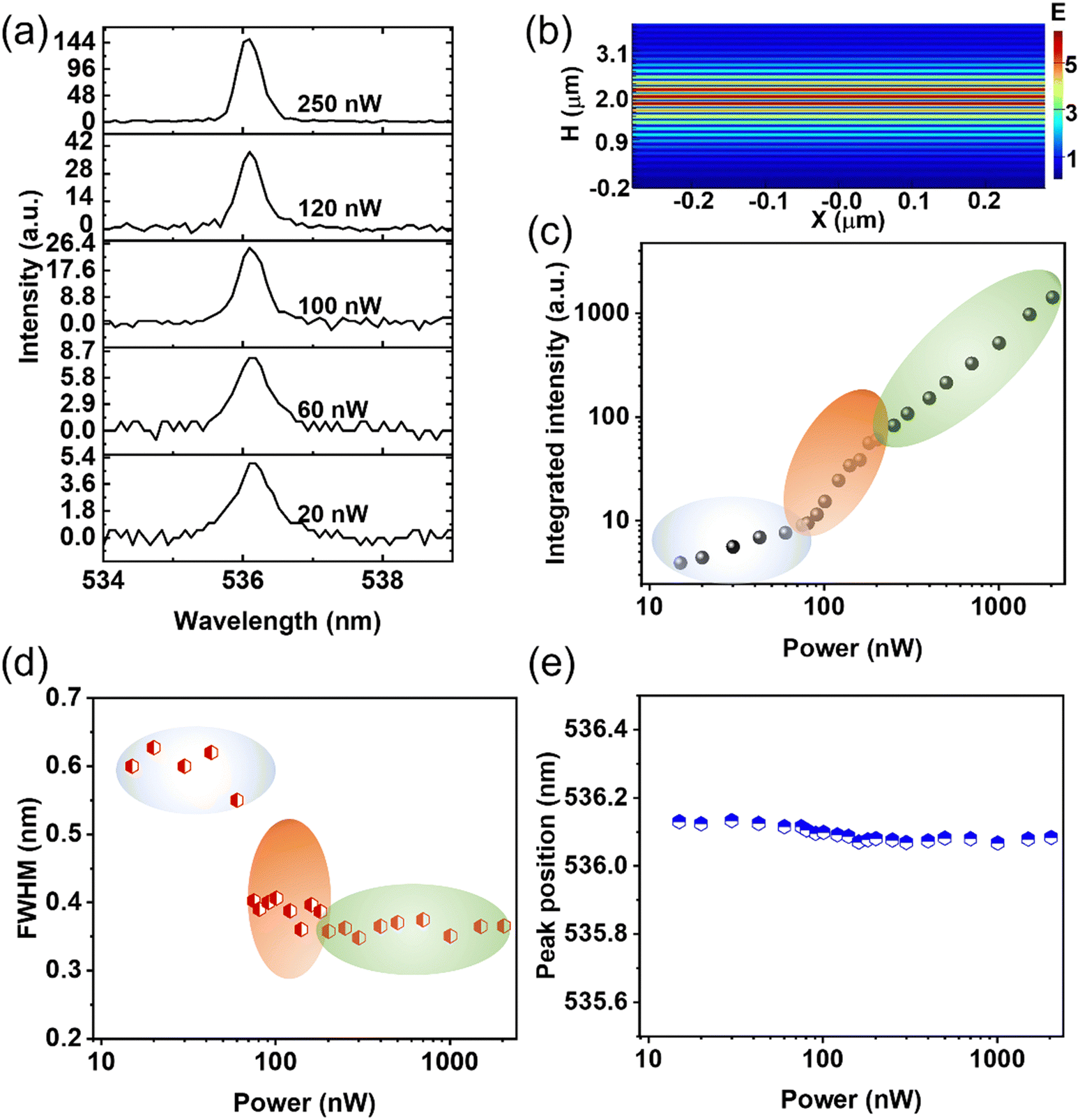 | ||
| Fig. 3 Lasing characterization of CsPbBr3 QDs VCSEL. (a) PL spectra collected at the zoomed-in range under varied excitation powers (≤250 nW). (b) Spatial electric field distribution of the calculated cavity mode (λ = 540.1 nm) inside the cavity along the vertical direction. The reference plane in the simulation model (H = 0) is defined at the bottom surface of the first layer TiO2. (c) Log–log plot of the emission intensity as a function of the excitation power. (d) The emission width as a function of the excitation power. The light blue, orange, and green regions represent the spontaneous emission state, superlinear amplification state, and lasing emission state, respectively. (e) The peak position of the emission as a function of the excitation power. | ||
To investigate the spatial distribution of lasing from the isolated CsPbBr3 QDs embedded in a microcavity, we carried out in situ PL mapping measurement (Fig. S2, ESI†). Accordingly, the evaluated density of the CsPbBr3 QDs is about 1.3 dots per μm2 (Fig. S6, ESI†), which is sparse enough to ensure the isolation of QDs and results in the possibility of isolated CsPbBr3 QDs operating in the full microcavity. Moreover, in comparison to the one (i.e., 5 nm) of a high-density ensemble of CsPbBr3 QDs, the PL width (i.e., 1.5 nm) of the isolated QD is considerably narrower (Fig. S3, ESI†). Such narrowing of PL results from the reduction of inhomogeneous broadening, which is an identifiable feature for isolated QDs.23–25
In addition, the optical response of the CsPbBr3 QDs VCSEL was explored layer by layer in depth via the confocal system along the z direction. In the confocal microscopic system, only the optical signals around the focal plane were probed while the out-of-focus signals were eliminated efficiently. Therefore, unlike the classical wide-field microscope, it offers a method to explore the optical response of the sample layer by layer in depth. The spontaneous emission (black curve in Fig. 2c) from the isolated QDs itself is usually well trapped inside the cavity due to strong optical confinement. The trapped photons oscillate inside the cavity, which is difficult to be directly probed by the confocal microscopic system. However, when the focal plane is moved inside the cavity, the spontaneous emission can be detected by the confocal microscopic system, which is called leaked spontaneous emission (LSE). In such a situation, the plane of the maximum LSE is the exact location of CsPbBr3 QDs near the top DBRs, while the plane of the maximum LE is located at the surface of the microcavity. The location of isolated CsPbBr3 QDs as the gain material is regarded as a reference plane. As the focal plane scans from the bottom (z = −9 μm) to the top (z = 9 μm), the extraordinary evolution of the profile of the PL spectrum comes out, as shown in Fig. 4a, where the maximum intensities of LE and LSE are located at different planes, zmaxLE = 1.2 ± 0.1 μm and zmaxLSE = −0.3 ± 0.1 μm, respectively. LSE diffuses randomly and lacks directionality with limited emission depth. In contrast, the z-axis emission range of LE is much more extensive, indicating less diffusion and more steadiness in space. In Fig. 4b, the contour map is zoomed-in for better recognition of the LE behavior with an asymmetric intensity profile (in red), which is reasonable since the LE has a preference to emit toward the outside vertically from the cavity surface. Such a distinctively directional feature is the most significant fingerprint of VCSEL.26,27 The normalized PL spectra taken in the QDs’ plane (black curve) and on the surface (red curve) are plotted in Fig. 4c, where their LSE and LE components are different. The PL spectrum taken at z = 2.5 μm is also plotted for comparison, which locates above the surface of the VCSEL. As the scanning objective lens rises from the QDs’ plane, the LSE decreases remarkably, while the LE becomes more and more prominent. The ratio of LE intensities can be defined as:

 | ||
| Fig. 4 Photoluminescence characterization of the as-fabricated CsPbBr3 QD VCSEL across the z-direction. The z-direction is defined as being perpendicular to the sample surface. (a) The contour map of the z-position-dependent PL intensity. The excitation power is 8 μW. (b) The zoomed-in contour map of the marked region in (a) with an asymmetric profile. (c) Normalized PL spectra taken at the QDs’ plane (black), surface (red), and z = 2.5 μm (blue), respectively. (d) The intensities of the lasing emission (LE) ratio to the complete emission intensities as a function of the z-position. ILE: the intensities of LE, ILSE: the intensities of leaked spontaneous emission (LSE). The inset illustrates the schematic of the directionality of LE (light yellow) versus the randomness of LSE (red). | ||
To study the stability of our device, we monitored the lasing behavior via confocal PL measurement over time. As shown in Fig. 5a, the as-fabricated CsPbBr3 QD VCSEL is continuously excited by a 488 nm laser with a power of 12 μW for 300 s and the emission spectra collected on a single sampling spot are plotted as the contour map of the time-dependent PL intensity. The integrated intensity of the lasing peak as a function of time is presented in Fig. 5b, in which the lasing is sustained for 300 s without an apparent reduction in intensity. The parallel PL measurement was conducted on the identical VCSEL device, which was stored in an ambient atmosphere for over one year in Fig. S4 (ESI†). Even though the performance of our VCSEL is not as good as a fresh one, its threshold and Q factor (over 1190) are comparable with those of the previous pumping single-mode perovskite lasers.12,22
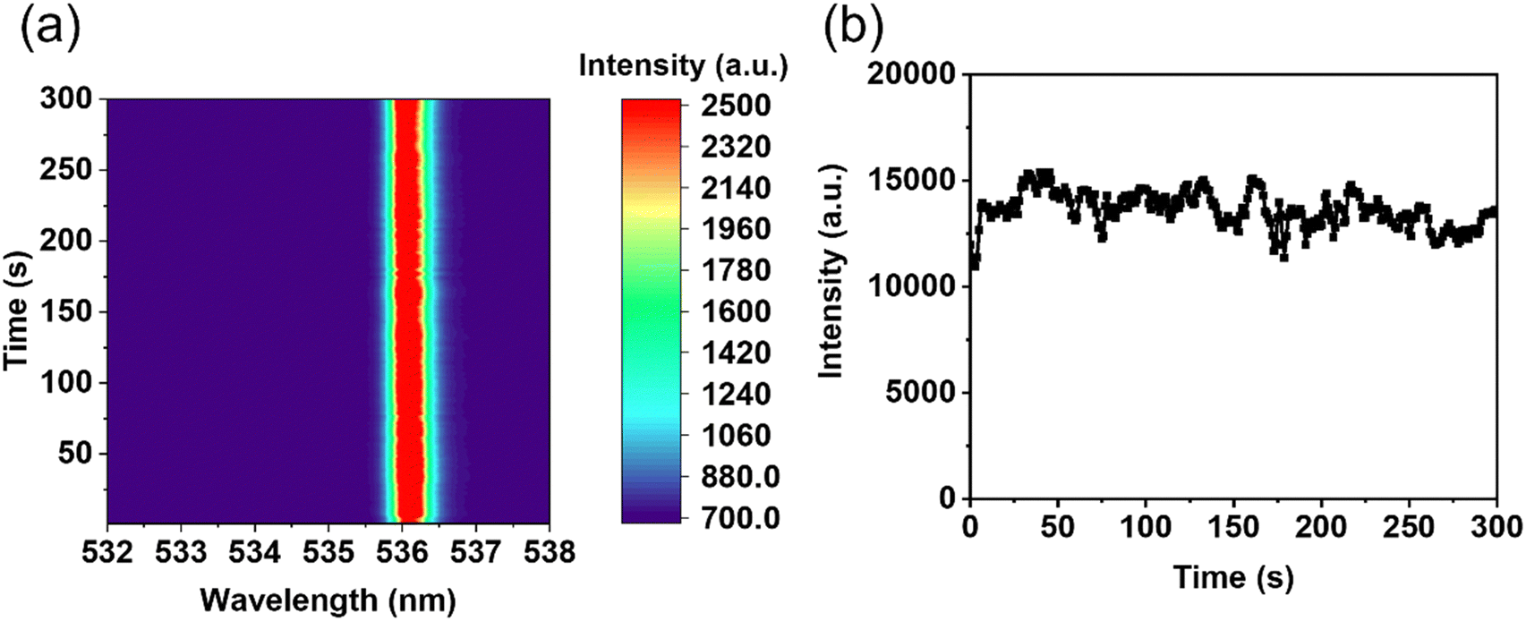 | ||
| Fig. 5 Stability of the as-fabricated CsPbBr3 QD VCSEL under continuous illumination. (a) The contour map of the time-dependent PL intensity. (b) The integrated emission intensity of lasing emission as a function of pumping time under 488 nm CW laser excitation at room temperature, under ambient atmosphere. The excitation power is 12 μW. | ||
Conclusions
High-quality CsPbBr3 QDs have been synthesized by a modified hot injection solution method, which exhibits outstanding light-emitting performance at room temperature. As-synthesized CsPbBr3 QDs were employed as the gain medium and sandwiched by two sets of high-reflectivity DBRs to form a high Q-factor vertical cavity surface emitting laser. The single-mode CW lasing with an ultra-low threshold of 8.8 W cm−2 has been observed at room temperature, which is verified by the intensity kink of the light input–output curve, the line width narrowing, and the spatially asymmetric emission. The discrete QDs were explored by low-temperature PL measurement and AFM, which were different from the high-density ensemble. The fabricated VCSEL device is stable and robust, and can be sustained for more than 300 s and conserves the lasing characteristic after one year of preservation. Our strategy to design and fabricate perovskite-QD VCSELs can easily be generalized to other perovskites with different emission wavelengths and paves the way toward single-dot coherent light sources and high-resolution displays based on perovskite QDs.Methods
We modified the hot-injection strategy to prepare CsPbBr3 QDs. Typically, PbBr2 (0.72 mmol), oleic acid (2.0 mL), oleylamine (2.0 mL), and octadecene (20 mL) were mixed in a two-neck flask and heated to 100 °C with strong stirring for 30 min. The container was kept in a vacuum by filling and evacuating N2. After all PbBr2 dissolved with continuous heating to 160 °C, the hot Cs-oleate precursor solution (2 mL) was injected. A few sec later, the reaction was stopped by using an ice bath. The product CsPbBr3 QDs were collected and washed with cyclohexane by centrifugation at 10![[thin space (1/6-em)]](https://www.rsc.org/images/entities/char_2009.gif) 000 rpm several times. Finally, the as-prepared CsPbBr3 QDs were conserved in 10 ml of cyclohexane.
000 rpm several times. Finally, the as-prepared CsPbBr3 QDs were conserved in 10 ml of cyclohexane.
The device was constructed on a commercial silica (300 nm)/silicon (0.5 mm) substrate. The high-purity (99.9%) SiO2, TiO2, and Ta2O5 sources were utilized for fabricating the bottom and top DBRs by using an e-beam evaporator (Cello, Ohmiker-50B) with a high vacuum (∼10−6 Torr), respectively. Before being spin-coated on the bottom DBR, our synthesized CsPbBr3 QDs were diluted by 1000 times and mixed with the PMMA.
Scanning electron microscopy (SEM) images and energy-dispersive X-ray spectroscopy (EDS) images were obtained using a Zeiss Auriga Dual-Beam FIB/SEM system. Transmission electron microscopy (TEM) images were acquired by using a JEM-ARM200F analytical electron microscope (JEOL). Atomic force microscopy (AFM) images were acquired by using an Asylum Research Cypher ES scanning probe microscope.
The PL and Raman measurements were conducted by using a confocal microscopic system (WITec, Alpha 300). A 488 nm excitation laser source was used for the PL measurement, while a 633 nm excitation laser source was used for the Raman measurement. A 50× objective lens (Nikon, LU Plan, NA = 0.55, WD = 10.1 mm) was used to focus the laser beam, with a spot size of 1.2 μm on the sample surface. The reflectivity spectra were collected from the backscattering configuration of the confocal microscopic system, in which a white-light source was used to irradiate the sample with a 20× objective lens (Zeiss, NA = 0.4, WD = 3.1 mm).
Conflicts of interest
The authors declare no competing financial interest.Acknowledgements
H. Z., W. W., and B. D. contributed equally to this work. This work is supported by the National Key R&D Program of China (2021YFA1200800), the Academic Research Fund Tier 1 (RG93/19), Singapore National Research Foundation (NRF) under the Competitive Research Programs (NRF-CRP-21-2018-0007), and the Agency for Science, Technology, and Research (A*STAR) under AME Individual Research Grant (AME-IRG-A20E5c0083, & A1883c0004). J. S. acknowledges support from the Fundamental Research Funds for the Central Universities of China, the Natural Science Foundation of China (Grant No. 61904151 and 61935017), and the Joint Research Funds of Department of Science and Technology of Shaanxi Province and Northwestern Polytechnical University (Grant No. 2020GXLH-Z-020). L. Z. was financially supported by grants from the Young Scientists Fund of the National Natural Science of China (No. 51902355). S. F. was supported by the H2020-MSCA-IF-2020 project SingExTr (Grant No. 101031596).References
- H. Zhou, Q. Chen, G. Li, S. Luo, T.-B. Song, H.-S. Duan, Z. Hong, J. You, Y. Liu and Y. Yang, Science, 2014, 345, 542–546 CrossRef CAS PubMed.
- X. Zhang, M. E. Turiansky and C. G. Van de Walle, J. Phys. Chem. C, 2020, 124, 6022–6027 CrossRef CAS.
- Z.-K. Tan, R. S. Moghaddam, M. L. Lai, P. Docampo, R. Higler, F. Deschler, M. Price, A. Sadhanala, L. M. Pazos and D. Credgington, Nat. Nanotechnol., 2014, 9, 687–692 CrossRef CAS PubMed.
- N. Wang, L. Cheng, R. Ge, S. Zhang, Y. Miao, W. Zou, C. Yi, Y. Sun, Y. Cao, R. Yang, Y. Wei, Q. Guo, Y. Ke, M. Yu, Y. Jin, Y. Liu, Q. Ding, D. Di, L. Yang, G. Xing, H. Tian, C. Jin, F. Gao, R. H. Friend, J. Wang and W. Huang, Nat. Photonics, 2016, 10, 699–704 CrossRef CAS.
- S. Yakunin, M. Sytnyk, D. Kriegner, S. Shrestha, M. Richter, G. J. Matt, H. Azimi, C. J. Brabec, J. Stangl and M. V. Kovalenko, Nat. Photonics, 2015, 9, 444 CrossRef CAS PubMed.
- C. Liu, K. Wang, P. Du, E. Wang, X. Gong and A. J. Heeger, Nanoscale, 2015, 7, 16460–16469 RSC.
- Q. Zhang, R. Su, W. Du, X. Liu, L. Zhao, S. T. Ha and Q. Xiong, Small Methods, 2017, 1, 1700163 CrossRef.
- G. Xing, N. Mathews, S. S. Lim, N. Yantara, X. Liu, D. Sabba, M. Grätzel, S. Mhaisalkar and T. C. Sum, Nat. Mater., 2014, 13, 476–480 CrossRef CAS PubMed.
- Y. Jia, R. A. Kerner, A. J. Grede, B. P. Rand and N. C. Giebink, Nat. Photonics, 2017, 11, 784–788 CrossRef CAS.
- S. W. Eaton, M. Lai, N. A. Gibson, A. B. Wong, L. Dou, J. Ma, L.-W. Wang, S. R. Leone and P. Yang, Proc. Natl. Acad. Sci. U. S. A., 2016, 113, 1993 CrossRef CAS PubMed.
- F. Di Stasio, S. Christodoulou, N. Huo and G. Konstantatos, Chem. Mater., 2017, 29, 7663–7667 CrossRef.
- L. Wang, L. Meng, L. Chen, S. Huang, X. Wu, G. Dai, L. Deng, J. Han, B. Zou, C. Zhang and H. Zhong, J. Phys. Chem. Lett., 2019, 10, 3248–3253 CrossRef CAS PubMed.
- Q. Chen, J. Wu, X. Ou, B. Huang, J. Almutlaq, A. A. Zhumekenov, X. Guan, S. Han, L. Liang, Z. Yi, J. Li, X. Xie, Y. Wang, Y. Li, D. Fan, D. B. L. Teh, A. H. All, O. F. Mohammed, O. M. Bakr, T. Wu, M. Bettinelli, H. Yang, W. Huang and X. Liu, Nature, 2018, 561, 88–93 CrossRef CAS PubMed.
- O. Yaffe, Y. Guo, L. Z. Tan, D. A. Egger, T. Hull, C. C. Stoumpos, F. Zheng, T. F. Heinz, L. Kronik, M. G. Kanatzidis, J. S. Owen, A. M. Rappe, M. A. Pimenta and L. E. Brus, Phys. Rev. Lett., 2017, 118, 136001 CrossRef PubMed.
- M. Liao, B. Shan and M. Li, J. Phys. Chem. Lett., 2019, 10, 1217–1225 CrossRef CAS PubMed.
- J.-H. Cha, J. H. Han, W. Yin, C. Park, Y. Park, T. K. Ahn, J. H. Cho and D.-Y. Jung, J. Phys. Chem. Lett., 2017, 8, 565–570 CrossRef CAS PubMed.
- C.-Y. Huang, C. Zou, C. Mao, K. L. Corp, Y.-C. Yao, Y.-J. Lee, C. W. Schlenker, A. K. Y. Jen and L. Y. Lin, ACS Photonics, 2017, 4, 2281–2289 CrossRef CAS.
- J. Shang, C. Cong, Z. Wang, N. Peimyoo, L. Wu, C. Zou, Y. Chen, X. Y. Chin, J. Wang, C. Soci, W. Huang and T. Yu, Nat. Commun., 2017, 8, 543 CrossRef PubMed.
- Y. Wang, X. Li, V. Nalla, H. Zeng and H. Sun, Adv. Funct. Mater., 2017, 27, 1605088 CrossRef.
- Y. Jia, R. A. Kerner, A. J. Grede, A. N. Brigeman, B. P. Rand and N. C. Giebink, Nano Lett., 2016, 16, 4624–4629 CrossRef CAS PubMed.
- H. Zhu, Y. Fu, F. Meng, X. Wu, Z. Gong, Q. Ding, M. V. Gustafsson, M. T. Trinh, S. Jin and X. Y. Zhu, Nat. Mater., 2015, 14, 636–642 CrossRef CAS PubMed.
- Z. Li, J. Moon, A. Gharajeh, R. Haroldson, R. Hawkins, W. Hu, A. Zakhidov and Q. Gu, ACS Nano, 2018, 12, 10968–10976 CrossRef CAS PubMed.
- Y.-S. Park, S. Guo, N. S. Makarov and V. I. Klimov, ACS Nano, 2015, 9, 10386–10393 CrossRef CAS PubMed.
- G. Rainò, G. Nedelcu, L. Protesescu, M. I. Bodnarchuk, M. V. Kovalenko, R. F. Mahrt and T. Stöferle, ACS Nano, 2016, 10, 2485–2490 CrossRef PubMed.
- M. Isarov, L. Z. Tan, M. I. Bodnarchuk, M. V. Kovalenko, A. M. Rappe and E. Lifshitz, Nano Lett., 2017, 17, 5020–5026 CrossRef CAS PubMed.
- K. J. Vahala, Nature, 2003, 424, 839–846 CrossRef CAS PubMed.
- E. Kapon and A. Sirbu, Nat. Photonics, 2009, 3, 27–29 CrossRef CAS.
- W. Zhou, M. Dridi, J. Y. Suh, C. H. Kim, D. T. Co, M. R. Wasielewski, G. C. Schatz and T. W. Odom, Nat. Nanotechnol., 2013, 8, 506–511 CrossRef CAS PubMed.
- Q. Zhang, S. T. Ha, X. Liu, T. C. Sum and Q. Xiong, Nano Lett., 2014, 14, 5995–6001 CrossRef CAS PubMed.
- S. Wu, S. Buckley, J. R. Schaibley, L. Feng, J. Yan, D. G. Mandrus, F. Hatami, W. Yao, J. Vučković, A. Majumdar and X. Xu, Nature, 2015, 520, 69–72 CrossRef CAS PubMed.
- Y. Ye, Z. J. Wong, X. Lu, X. Ni, H. Zhu, X. Chen, Y. Wang and X. Zhang, Nat. Photonics, 2015, 9, 733–737 CrossRef CAS.
- Y. Li, J. Zhang, D. Huang, H. Sun, F. Fan, J. Feng, Z. Wang and C. Z. Ning, Nat. Nanotechnol., 2017, 12, 987–992 CrossRef CAS PubMed.
Footnotes |
| † Electronic supplementary information (ESI) available. See DOI: https://doi.org/10.1039/d3nh00139c |
| ‡ The authors contributed equally to this work. |
| This journal is © The Royal Society of Chemistry 2023 |