
 Open Access Article
 This Open Access Article is licensed under a
 Creative Commons Attribution 3.0 Unported Licence
Silicon phthalocyanine-based n-type organic mixed ionic-electronic conductor in organic electrochemical transistors†
May Ourabi a,
Mario C. Vebberab,
Mélanie Cyrab,
Forest St-Denis Weintragera,
Nicolas Ledosab,
Halynne R. Lamontagneab,
Audithya Nyayachavadia,
Jaclyn L. Brussob and
Benoît H. Lessard*ac
a,
Mario C. Vebberab,
Mélanie Cyrab,
Forest St-Denis Weintragera,
Nicolas Ledosab,
Halynne R. Lamontagneab,
Audithya Nyayachavadia,
Jaclyn L. Brussob and
Benoît H. Lessard*ac
aDepartment of Chemical and Biological Engineering, University of Ottawa, 161 Louis Pasteur, Ottawa, ON, Canada. E-mail: benoit.lessard@uottawa.ca
bDepartment of Chemistry and Biomolecular Sciences, University of Ottawa, 150 Louis Pasteur, Ottawa, ON, Canada
cSchool of Electrical Engineering and Computer Science, University of Ottawa, 800 King Edward Ave., Ottawa, ON, Canada
First published on 8th July 2025
Abstract
Phthalocyanines have evolved from their early role as dyes and pigments into a versatile class of small-molecule semiconductors used in thin-film electronics, including organic photovoltaics and thin-film transistors. Using a silicon phthalocyanine with hydrophilic (2-[2-(2-methoxyethoxy)ethoxy]acetate) axial substitutions, we report the first application of phthalocyanine films as an n-type organic mixed ionic-electronic conductor material in organic electrochemical transistors. The devices demonstrate a figure of merit (μC*) of 0.011 F cm−1 V−1 s−1, volumetric capacitance (C*) of 79.3 F cm−3 and resulting charge mobility (μ) of 1.4 × 10⁻⁴ cm2 V−1 s−1. Characterization of the films using atomic force microscopy and Raman spectroscopy points towards a rearrangement of the thin films post-swelling, which ultimately results in poor cycling stability. Nonetheless, this application broadens the use of phthalocyanines and enlarges the library of organic mixed ionic-electronic conductors to include this inexpensive and biocompatible material.
1. Introduction
Organic mixed ionic-electronic conductors (OMIECs) are a class of materials capable of transporting both ionic and electronic charges simultaneously when employed in electrolyte-based devices, such as organic electrochemical transistors (OECTs).1 Interest in these devices has surged owing to their low operating voltages and operability in aqueous environments, making them a promising fit for integration into biological systems.2,3 Unlike electrolyte-gated organic field-effect transistors (EGOFETs), they allow for permeation of ions into the entire film, thereby increasing the capacitance of the bulk.4 OMIEC materials are often engineered by affixing pegylated sidechains onto a common semiconductor building block to enable their film to swell with hydrated ions upon doping.5–7Though they are less ubiquitous than polymeric OMIECs, small molecules such as fullerene,8 naphthalene diimide9,10 (NDI), perylene diimide11,12 (PDI), naphthalene bis-isatin13 and IDIC14 have been modified to be employed as OMIECs in OECTs. A major motivation for the development of small molecule OMIECs is the reduced batch-to-batch variation, in addition to their clearly defined chemical structure which facilitates the establishment of structure–property relationships.15 As is the case for other organic semiconductors, there also exists a wide range of synthetic complexity depending on their molecular structure. For example, our group has demonstrated that silicon phthalocyanine (R2-SiPc) derivatives have a far lower synthetic complexity index than other non-fullerene acceptors, yet achieve modest performance in organic photovoltaics.16
Phthalocyanines have found some use in EGOFETs, but their use in OECTs remains limited. More precisely, copper phthalocyanine (CuPc) has been employed in p-type EGOFETs due to its low cost and low toxicity,17,18 and there is some precedent for the use of CuPc in OECTs in recent literature. In the work produced by Ferro et al., this was achieved in sublimed films of CuPc by decreasing measurement time below the ionic displacement time constant, thereby switching from EGOFET operation to OECT operation.19 This method exploits the presence of nano-scale vacancies in the film structure and allows for ions to occupy them in order to dope the semiconductor. A similar strategy was employed by Luzio et al., who dissolved CuPc in trifluoroacetic acid to cast porous films, which were then transferred to the device substrates by delamination in an ethanol bath.20 However, these examples pose some issues for scalability, as CuPc is not easily solubilized and must often be thermally evaporated. It also inherently operates as a p-type semiconductor that cannot easily be modified into an n-type material due to its intrinsic nature. Meanwhile, R2-SiPc molecules are tetravalent, enabling axial substitutions in addition to peripheral substitutions, which provide handles to fine tune the molecular structure and material properties such as solubility, solid state stacking and other film forming characteristics.21,22
These chemical handles have previously been used to affix pegylated chains of varying lengths in the literature,23–27 often with the goal of rendering them water soluble for use in photodynamic therapy applications.21 More recently, Ivanova et al. evaluated the use of various pegylated SiPc derivatives in chemiresistor-based ammonia sensors.28 Other R2-SiPcs have been reported as predominantly n-type semiconductors in organic thin-film transistors29–32 (OTFTs) and organic photovoltaics33,34 (OPVs). In this study, we report the first n-type phthalocyanine-based OMIEC and the first OECT based on a R2-SiPc, which was achieved using 2-[2-(2-methoxyethoxy)ethoxy]acetate (MEEA) axial substitutions. The resulting compound was integrated into OTFTs and OECTs, where it achieved μC* = 0.011 F cm−1 V−1 s−1. The material and resulting films were characterized using cyclic voltammetry, UV-Vis spectroscopy, X-ray diffraction (XRD) and grazing incidence wide-angle X-ray spectroscopy (GIWAXS), as well as atomic force microscopy (AFM) and Raman spectroscopy before and after swelling to rationalize the poor cycling stability of the devices.
2. Methods
2.1. Materials
Dichlorosilicon phthalocyanine (Cl2-SiPc) was synthesized following previously reported procedures.35 2-[2-(2-methoxyethoxy)ethoxy]acetic acid was purchased from Millipore-Sigma (PN#407003). All solvents used were commercially obtained and employed without additional purification.2.2. MEEA-SiPc synthesis
To a 100 mL round-bottom flask equipped with a magnetic stir bar, chlorobenzene (30 mL), Cl2-SiPc (1.0 g, 1.6 mmol), and excess 2-[2-(2-methoxyethoxy)ethoxy]acetic acid (2.5 mL, 16 mmol) were added. The reaction mixture was purged with nitrogen gas for 15 minutes and heated under reflux at 132 °C for 16 hours. After cooling to room temperature, the resulting dark-teal solution was filtered through filter paper to remove any unreacted SiPc. The residue was washed three times with chlorobenzene (10 mL each). The filtrate was concentrated under reduced pressure to yield a dark oily residue. The crude product was then precipitated by the addition of cold methanol (50 mL), and the solid product was separated by filtration. The precipitate was washed three times with cold methanol. Product purification was achieved via Soxhlet extraction in iso-propanol (250 mL), followed by recrystallization in iso-propanol to yield the title product as a blue powder (0.34 g, 21%). The structure of the product was confirmed by 1H NMR and 13C NMR, seen in Fig. S2 and S3 (ESI†), and single-crystal X-ray diffraction, seen in Fig. S4 (ESI†). 1H NMR (400 MHz, CDCl3) δ (ppm): 9.71–9.68 (m, 8H), 8.41–8.37 (m, 8H), 3.07–3.05 (m, 10H), 2.97–2.88 (m, 4H), 2.51–2.47 (m, 4H), 1.80–1.76 (m, 4H), 1.01 (s, 4H). 13C NMR (151 MHz, CDCl3) δ (ppm): 163.72, 150.18, 135.72, 131.55, 124.18, 71.51, 69.91, 69.51, 68.68, 66.93, 58.84.2.3. Cyclic voltammetry
The in-solution electrochemical experiments were carried out under argon using a Bioanalytical Systems Inc. (BASi) Epsilon potentiostat with C3 cell stand and a glass cell, and were recorded using BASi Epsilon EC software V 2.13.77. For cyclic voltammetry with the three-electrode configuration, the working electrode was a platinum disk (d = 1.6 mm), and the reference and counter electrodes were both platinum wires. All potentials were internally referenced to the ferrocene/ferrocenium couple over a range from 0.82 V to −1.83 V bidirectionally. For the measurements, a concentration of 10−3 M of the electroactive species was used in freshly distilled and degassed dichloromethane and 0.1 M tetrabutylammonium hexafluorophosphate.Cyclic voltammetry on the MEEA-SiPc film was conducted in a 0.1 M NaCl solution using a PalmSens EmStat4 potentiostat and glass/ITO/MEEA-SiPc as the working electrode, a platinum wire as the counter electrode and an Ag/AgCl reference electrode filled with 3 M KCl (Redox.me). The scan rate was varied from 25 to 1000 mV s−1 from 0 V to −1.0 V.
2.4. UV-Vis-NIR spectroscopy
A Cary 6000i UV-Vis-NIR spectrophotometer was used to collect spectra from a dilute MEEA-SiPc solution in chloroform and a film cast on a glass substrate. Ex situ spectroelectrochemistry was performed by first applying a potential for 5 minutes with the equipment used for cyclic voltammetry on the MEEA-SiPc film. The film was then placed in the spectrophotometer to collect the absorption spectrum and returned to the electrochemical cell. This was repeated for potentials from −0.1 V to −0.9 V.2.5. Film characterization
AFM images were obtained from films cast on SiO2 substrates using a Bruker FastScan AFM loaded with ScanAsyst-Air tips at a scan rate of 1.72 Hz in ScanAsyst mode. Nanoscope Analysis v.3.0 was then used to flatten the images and determine the corresponding film roughness.GIWAXS experiments were conducted at the SIRIUS beamline at the SOLEIL Synchrotron facility in Saint-Aubin, France. The beam energy was 10 keV. The samples were placed in a closed chamber filled with He gas at a calculated distance of 312 mm from a Pilatus3 detector (Dextris) placed at a 9.9° angle and using an incident angle of α = 0.15°. Spectra were derived from the sum of 10 images using a 10 second exposure time per image. The data was calibrated against silver behenate and poly(3-hexylthiophene-2,5-diyl) standards and analysed using the GIXSGUI package in MATLAB.36
The film thickness was obtained by scratching off a portion of the semiconductor film and measuring the difference in profile with a Dektak XT profilometer.
2.6. Raman spectroscopy
A Renishaw InVia Qontor confocal Raman microscope was used to collect Raman spectra of the pristine and swelled films of MEEA-SiPc. Data were collected as maps of films between the source and drain electrodes of tested devices for the swelled films, and untested devices for the unswelled films. Measurements were centred around 1175 cm−1 and obtained using a 532 nm laser in streamline mapping mode with an exposure time of 1.2 s at an intensity of 50%, corresponding to 250 mW. Prior to data collection, calibration was performed against an internal silicon sample to ensure that the measurement was within 0.5 cm−1 of its 520 cm−1 peak.2.7. Electrochemical impedance spectroscopy
Electrodes composed of 2 nm of Cr and 50 nm of Au were deposited using physical vapour deposition (Angstrom Engineering EvoVac Thermal Evaporator) onto Si/SiO2 substrates. A 10 mg mL−1 solution of MEEA-SiPc was prepared in a nitrogen glovebox environment using dry chloroform and subsequently filtered through a 22 μm pore PTFE filter. The solution was then statically spin-cast onto the substrates at 1500 rpm for 90 seconds. The films were annealed at 70 °C for 1 hour under vacuum. The substrates were then placed in an electrolyte-gated transistor mount cell (Redox.me) to expose a predetermined surface area of the electrode/semiconductor to the electrolyte. The gold electrode then served as the working electrode in a three-electrode system to perform electrochemical impedance spectroscopy. A spiral platinum electrode and an Ag/AgCl reference electrode (Redox.me) were used as the counter and reference electrode, respectively. A PalmSens EmStat4 potentiostat was used to apply VAC = 0.01 V and gradually increase VDC from 0.0 to −0.9 V.PSTrace 5.9 was then used to fit a R(Q[R(QR)]) circuit to the results, which is adapted from Kovacs circuit37 but features constant phase angle elements (Q) instead of a capacitor to describe the double-layer and volumetric capacitance terms. The characteristic parameters from the constant phase element, Q and n, were converted to capacitance using the following relationship, where  is the angular frequency at maximum imaginary impedance, Z′′.38

2.8. OTFT fabrication and characterization
Generation 5 15 mm × 15 mm Si wafers with a 230 nm thermally grown layer of SiO2 were purchased from Fraunhofer IPMS. The wafers have 16 sets of prepatterned interdigitated source and drain electrodes, with channel widths of 2 mm and lengths of 2.5 μm, 5 μm, 10 μm and 20 μm. This translated to n = 4 devices for each channel length. A rinsing step with acetone and isopropanol was first performed to remove photoresist from the chips. The MEEA-SiPc films were cast as described previously, and the chips were placed into an oesProbeA10000-P290 probe station (Element Instrumentation Inc. and Kreus Design Inc.) under nitrogen without exposing the devices to air. A custom LabVIEW program and a Keithley 2614B sourcemeter were used to collect output and transfer characteristics. For the former, constant VGS values between 0 and 50 V with 10 V steps were applied while sweeping VDS from 0 to 50 V, while a constant VDS of 50 V was applied while sweeping VGS bidirectionally from 0 to 50 V for the latter. Each device was subjected to four transfer curve measurements. Threshold voltage (VT) and electron mobility (μe) were calculated in the saturation regime by plotting the square root of IDS against VGS, based on the following drain current relationship from the MOSFET equation.where μe is the electron mobility of the semiconductor, Ci is the areal capacitance of the SiO2 dielectric, and W and L represent the width and length of the channel, respectively.
2.9. OECT fabrication and characterization
Generation AX1580 15 mm × 15 mm Si/SiO2 wafers with eight sets of prepatterned interdigitated source and drain electrodes were purchased from Fraunhofer IPMS. Each substrate features two devices with a channel width of 10 mm and lengths of 2.5 μm, 5 μm, 10 μm and 20 μm. The rinsing and spin-coating steps were performed as described in the previous sections. Excess MEEA-SiPc was removed from the source and drain electrodes using a cotton applicator soaked in chloroform, and a nail polish top-coat (Sally Hansen Insta-Dry Top-Coat) was applied over the exposed electrode to form an encapsulating nitrocellulose layer. The substrates were then placed in a machined Teflon mount to hold a well filled with 0.1 M NaCl over the device channels while allowing access for the probes to contact the device pads. The electrolyte solution was bubbled with nitrogen for 5 minutes prior to testing. An Ag/AgCl reference electrode was then placed in the well and used as a gate electrode.I–V curves were collected using a Keithley 2614B sourcemeter interfaced with a custom program in LabVIEW. Output characteristics were obtained by sweeping VDS from −0.1 to 0.7 V and increasing VGS from 0.0 to 0.7 V. Transfer characteristics were collected in the saturation regime with VDS = 0.6 V by sweeping VGS from −0.2 to 0.7 V at a rate of 30 mV s−1. Transfer curve acquisitions were repeated 10 times to ensure the signal had stabilized. The threshold voltage was taken as the x-axis intercept of the linear slope of  , while the value of μC* was determined by plotting the maximum gm value against the product of
  , as described by the equation:
3. Results and discussion
3.1. MEEA-SiPc synthesis and characterization
Bis(2-[2-(2-methoxyethoxy)ethoxy]acetate) silicon phthalocyanine (MEEA-SiPc), shown in Fig. 1a, is obtained directly in one step from the nucleophilic substitution of Cl2-SiPc with 2-[2-(2-methoxyethoxy)ethoxy]acetate in refluxing chlorobenzene with a yield of 21% (see Fig. S1, ESI†). MEEA-SiPc was thoroughly characterized using nuclear magnetic resonance spectroscopy (1H-NMR and 13C-NMR), as shown in Fig. S2 and S3 (ESI†), and single-crystal X-ray diffraction (XRD), as shown in Fig. S4 (ESI†) (CCDC #2455373). From the latter technique, we observe that the interactions between MEEA chains disrupt the SiPc cores’ ability to form good π–π interactions with one another along most planes, although some herringbone patterns do form within the unit cell. When spin-coated into a film, the MEEA-SiPc had a water contact angle of 74.8° ± 1.6°. | ||
| Fig. 1 (a) Chemical structure of MEEA-SiPc. (b) Cyclic voltammetry of a MEEA-SiPc solution in DCM with added TBAP at a scan rate of 100 mV s−1. Potentials are reported against the oxidation of ferrocene. (c) UV-Vis spectrum of the MEEA-SiPc solution in chloroform and MEEA-SiPc film on a glass wafer. | ||
A combination of cyclic voltammetry and UV-Vis spectroscopy was used to determine the optoelectronic properties of the MEEA-SiPc, as shown in Table 1. The highest occupied molecular orbital (HOMO) and lowest unoccupied molecular orbital (LUMO) levels reported are similar to typical R2-SiPc derivatives.34 The electrochemical behaviour of MEEA-SiPc was studied by cyclic voltammetry in a dichloromethane (DCM) solution (c ≈ 1 mmol L−1), seen in Fig. 1b. The compound displays two reversible reduction processes (Eonsetred = −1.03 V vs. Fc+/Fc and Eonsetred = −1.38 V vs. Fc+/Fc) and a reversible oxidation process (Eonsetox = +0.54 V vs. Fc+/Fc), indicating excellent electrochemical stability and an accessible LUMO level for n-type operation. Cyclic voltammetry was also performed on the cast MEEA-SiPc film in 0.1 M NaCl (Fig. S5, ESI†).
| Semiconductor | λmax (solution)/(film) | Ebg![[thin space (1/6-em)]](https://www.rsc.org/images/entities/char_2009.gif) (solution)/(film)a (solution)/(film)a |
Eoxb | EHOMOc | ELUMO(solution)(film)d |
|---|---|---|---|---|---|
| (nm) | (eV) | (eV) | (eV) | (eV) | |
| a Ebg, bandgap determined from onset frequency of absorption in UV-Vis spectrum.b Eox, oxidation energy defined as onset of oxidation in cyclic voltammetry in DCM vs. ferrocene.c EHOMO, highest occupied molecular orbital energy level calculated from empirical correlation: EHOMO = − (Eox − Eox Ferrocene) − 4.8.d ELUMO, lowest unoccupied molecular orbital energy level obtained from the sum of EHOMO and Ebg. | |||||
| MEEA-SiPc | 686/712 | 1.77/1.60 | 0.54 | −5.3 | −3.6/−3.7 |
Additionally, UV-Vis spectroscopy was performed in both a chloroform solution and on a film of MEEA-SiPc (Fig. 1c). The MEEA-SiPc solution displayed an absorption profile with a Soret band between 300 and 400 nm and a Q-band with a peak at 686 nm, which are typical of soluble phthalocyanines.16,39 The MEEA-SiPc film displayed a broadening of the Q-band peak and a red-shift to 712 nm, indicative of aggregation and packing of the aromatic macrocycle of the phthalocyanines. Similar peak broadening and shifting going from solution to solid state have been reported for R2-SiPcs.40
The surface morphology of the MEEA-SiPc films was studied using AFM, XRD and GIWAXS. Pristine films of MEEA-SiPc exhibited large grain boundaries with deep cavities, as shown in AFM imaging in Fig. 2a. As the depth of these cavities somewhat aligns with the depth between the MEEA-SiPc and the exposed substrate (Fig. S6, ESI†), we understand them to be either a thin underlying layer of MEEA-SiPc or areas where the film did not adequately coat the substrate. Excluding these areas, the root mean square roughness of the film is 14.0 nm, which has been observed in other solution-processed R2-SiPc films.30 As the films were swelled by applying a −0.7 V potential, equivalent to the maximum voltage applied to the channel during OECT operation, the film roughness doubled to 29.2 nm and took on a fibrous morphology, as seen in Fig. 2b. Similar changes in grain appearance were observed by Liao et al. upon doping of a PDI-based small molecule, 4CL-PDI-4EG, although the authors also report a decrease in film roughness.11
 | ||
| Fig. 2 AFM image of the MEEA-SiPc film on SiO2 (a) before and (b) after doping at −0.7 V. (c) Diffraction pattern obtained from XRD and the GIWAXS q-cut compared against the predicted XRD spectrum. Data collected from GIWAXS was corrected to account for different excitation wavelengths, from λ = 1.24 Å−1 to λ = 1.54 Å−1. (d) 2D GIWAXS scattering pattern of a MEEA-SiPc film cast on SiO2. (e) Depiction of the MEEA-SiPc orientation relative to substrate determined using GIWAXS. The (101) plane is parallel to the substrate. | ||
XRD and GIWAXS were used to characterize as-cast MEEA-SiPc films on SiO2 substrates, as seen in Fig. 2c and d. Results obtained on Si substrates are shown in Fig. S7a and b (ESI†). Thin film XRD revealed the presence of three peaks of comparable intensity at 2θ = 6.9°, 8.2° and 9.0°. However, the simulated diffractogram of the isolated polymorph matches only the peak at 2θ = 8.2°, with two peaks attributed to (002) and (020). Thus, MEEA-SiPc films on SiO2 substrates are composed of at least two polymorphs, one of which is the structure resolved in this paper. On Si substrates, the unattributed peaks appear relatively less intense than the peaks that align with the identified polymorph, indicating that the surface is further influencing MEEA-SiPc to adopt a morphology distinct from its bulk organization.
The GIWAXS diffraction map of the MEEA-SiPc film on SiO2 displays short, well located, arcs. These features are typical of partially ordered crystalline films.41,42 Several reflection spots associated with the polymorph identified from single-crystal XRD could be indexed onto the 2D scattering pattern obtained from GIWAXS (Fig. S8, ESI†). By varying the primary orientation and generating the predicted peak locations associated with each orientation to align with collected GIWAXS data, we also conclude that the (101) planes of the crystallite are primarily parallel to the substrate, as shown in Fig. 2e. Given this orientation, it is likely that OTFT performance will suffer, as the orientation of the π–π stacking is opposite to charge transport. Distances between key MEEA-SiPc aromatic rings are shown in Fig. S4c (ESI†).
Electrochemical impedance spectroscopy (EIS) was performed on the MEEA-SiPc film in 0.1 M NaCl (Fig. 3). The data demonstrated a significant contribution from the double layer capacitance (Cdl) in the total capacitance of the system at low applied voltages. This is denoted by the phase angle at low frequencies, which decreases below 90° rather than reaching a plateau.43 In order to accurately extract the volumetric capacitance (C*) term, an equivalent circuit based on Kovacs circuit was used, as shown in Fig. 3a.37,44 Constant phase elements, represented as Q, were included in the circuit instead of capacitors to better approximate the behaviour of an imperfect capacitor, resulting in a Q1 and Q2 term, which represent the electrical double layer capacitance and C*, respectively. This strategy has been applied in literature – notably with the use of relatively hydrophobic OMIECs.45 The simulated circuit shows good agreement with the experimental data, as seen in Fig. 3b and c. As the applied voltage increases beyond −0.4 V vs. Ag/AgCl, C* also increases, suggesting ionic intake in the film. It then reaches a plateau at voltages beyond −0.7 V, where C* is equal to 79.3 ± 8.6 F cm−3.
 | ||
| Fig. 3 Electrochemical impedance spectroscopy (EIS) on the MEEA-SiPc film in 0.1 M NaCl. (a) Equivalent circuit used to fit experimental data. (b) Nyquist and (c) Bode plots obtained from the film with applied VDC = −0.7 V. Experimental and simulated data are shown as discrete points and dotted lines, respectively. X2 = 0.0001. | ||
The effect of applied voltage on the EIS data is shown in Fig. S9 (ESI†). Similarly, spectroelectrochemistry on the MEEA-SiPc film demonstrated a reduction in the π–π* transition peaks from applied potentials beyond −0.5 V, as seen in Fig. S10 (ESI†). These results suggest that the MEEA-SiPc will swell with ions during OECT operation, making it a suitable OMIEC.
3.2. Organic thin-film transistors
Bottom-gate bottom-contact (BGBC) OTFTs were fabricated using a spin-coated MEEA-SiPc film as the semiconductor on Si/SiO2 substrates with prepatterned ITO/Au electrodes. Representative output and transfer curves obtained from devices with L = 2.5 μm and W = 2000 μm are shown in Fig. 4, while representative curves from devices with channel lengths between 2.5 μm and 20 μm can be found in Fig. S11 (ESI†). Device performance metrics are shown in Table S1 (ESI†). In devices with shorter channel lengths of 2.5 μm, a threshold voltage (VT) of 6.6 ± 1.7 V was obtained, which is similar to R2-SiPc OTFTs with electron donating groups in the axial position.46 The average electron mobility (μe) of 1.01 ± 0.14 × 10⁻⁵ cm2 V−1 s−1 and on/off current ratio (ION/OFF) of 102 are modest for R2-SiPc based OTFTs and likely a result of the large grain boundaries seen in Fig. 2a. This could also be due to poor intermolecular stacking afforded by the MEEA chains, disrupting the potential to form strong π–π interactions between the macrocycles (Fig. S4, ESI†). R2-SiPc OTFTs typically demonstrate similarly poor performance when fabricated on untreated SiO2 but show significant improvements when using silane-treated surfaces due to improved film formation and the elimination of surface traps.22,47 Overall, these results demonstrate that MEEA-SiPc is an effective semiconductor for use in n-type devices. | ||
| Fig. 4 (a) Schematic of the MEEA-SiPc OTFT. Characteristic (b) output and (c) transfer curves of BGBC MEEA-SiPc OTFTs with W = 2000 μm, L = 2.5 μm. | ||
3.3. Organic electrochemical transistors
A similar fabrication procedure was used to fabricate OECTs on Si/SiO2 substrates with prepatterned electrodes. The devices were tested using 0.1 M NaCl and an Ag/AgCl reference electrode as the gate. An example of the output and transfer characteristics collected from the OECT with L = 2.5 μm and W = 10000 μm is shown in Fig. 5, while curves collected from devices with other channel dimensions are shown in Fig. S12 (ESI†). The devices display good saturation of the source-drain current (IDS) in the output curves. The calculated VT of 0.595 ± 0.031 V is in agreement with the rapid increase in volumetric capacitance observed from EIS from −0.4 V to −0.7 V. A summary of the device performance parameters extracted from the I–V characteristics is shown in Table 2. The figure of merit, μC*, obtained from the results is 0.0111 ± 0.0006 F cm−1 V−1 s−1, which is on the same order of magnitude as PDI with simple tri-ethylene glycol additions to the core,11 and an order of magnitude below other small molecule OMIECs.8,9,11 The derived charge mobility, μ, is 1.4 × 10⁻⁴ cm2 V−1 s−1, which is also on the same order as other n-type small molecules. This suggests that the dominant issue with the MEEA-SiPc performance is the relatively low C* achieved during swelling.8,9,11 The devices also display high leakage currents due to some exposed areas of the source and drain electrodes. Nonetheless, this is a promising first demonstration of R2-SiPc OMIECs.
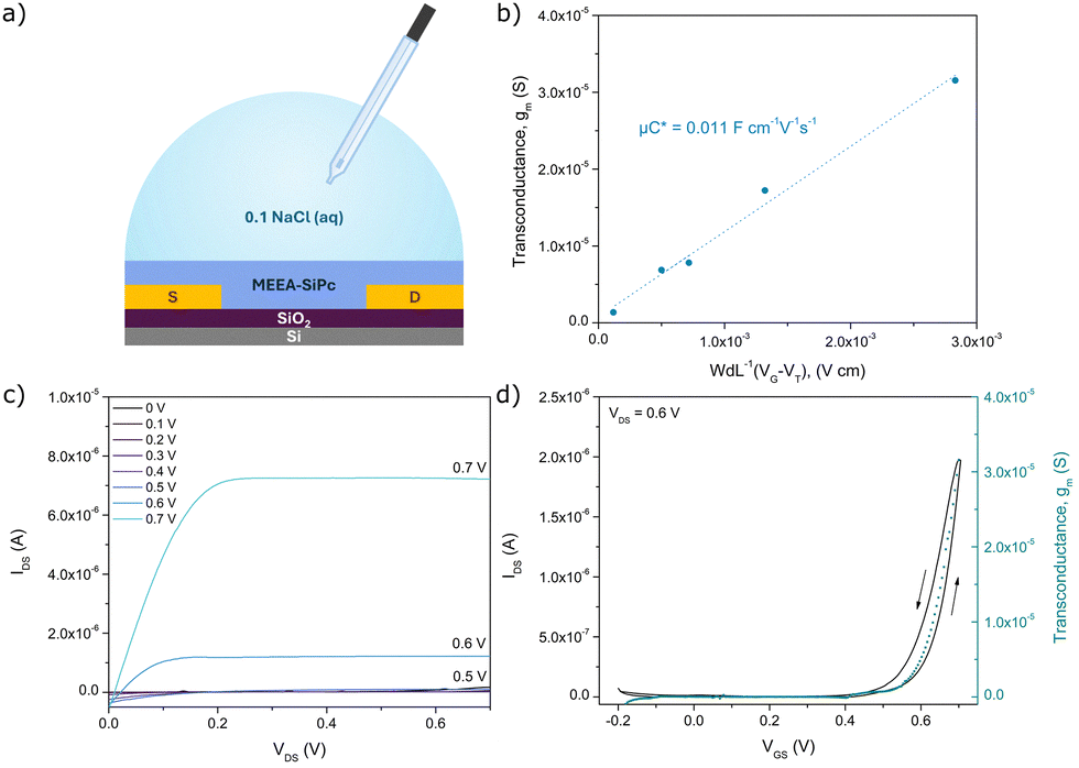 | ||
| Fig. 5 (a) Schematic of the MEEA-SiPc OECT. (b) Determination of μC* from the plot of gm vs. WdL-1(VG − VT). Characteristic (c) output and (d) transfer curves of MEEA-SiPc OECTs in 0.1 M NaCl with W = 10000 μm, L = 2.5 μm. | ||
| Semiconductor | d | VTa | gmnormb |
μC*c | C*d | μe | ION/OFF |
|---|---|---|---|---|---|---|---|
| (nm) | (V) | (S cm−1) | (F cm−1 V−1 s−1) | (F cm−3) | (cm2 V−1 s−1) | (—) | |
a VT, threshold voltage determined from the x-axis intercept of the  curve.b gm curve.b gm![[thin space (1/6-em)]](https://www.rsc.org/images/entities/i_char_2009.gif) norm, normalized maximum transconductance divided by the channel dimensions Wd/L.c μC* determined by the slope of Fig. 5b.d C* obtained from EIS at −0.7 V. See Fig. S9 (ESI).e μ obtained by dividing the μC* figure of merit by C*. norm, normalized maximum transconductance divided by the channel dimensions Wd/L.c μC* determined by the slope of Fig. 5b.d C* obtained from EIS at −0.7 V. See Fig. S9 (ESI).e μ obtained by dividing the μC* figure of merit by C*. |
|||||||
| MEEA-SiPc | 54.3 ± 2.4 | 0.595 ± 0.031 | 0.00143 ± 0.00045 | 0.0111 ± 0.0006 | 79.3 ± 8.6 | 1.4 × 10⁻⁴ | 101–103 |
The rapid decrease in device current shown in the transient characteristics (Fig. 6a) illustrates the lack of operational stability of the MEEA-SiPc OECTs. This can be partially attributed to the shallow LUMO level of the small molecule, as well as the structural reorganization of the thin film presented in AFM images. Optical microscopy of the films on repeatedly tested devices, shown in Fig. 6b, also reveals the formation of aggregates surrounded by areas wherein the film has delaminated from the electrodes, reducing the effective W/L ratio of the device. This is likely caused by repeated swelling and deswelling of the MEEA-SiPc film, causing the MEEA-SiPc to aggregate. The Raman spectra collected from swelled regions also differed from those collected from unswelled regions, as seen in Fig. 6c. The B1g band, which is related to Cα–Nβ–Cα in-plane vibrations, exhibited a relative increase in intensity and a shift from 1556 cm−1 to 1541 cm−1. This may suggest that a larger proportion of the MEEA-SiPc is oriented parallel to the substrate than prior to swelling.48 Downward shifts in the B1g band have also been associated with stronger π–π interactions.49
 | ||
| Fig. 6 (a) Transient characteristics of the MEEA-SiPc OECT with W = 10000 μm, L = 2.5 μm. (b) Optical microscope image of the device after cycling. (c) Raman spectra of the swelled and unswelled regions of the MEEA-SiPc film. | ||
In an effort to prevent film delamination and increase device stability, devices were fabricated with a 5 wt% loading of polyethylene glycol (PEG) in the MEEA-SiPc solution prior to spin-coating. This rationale wherein a polymer electrolyte is blended with a less efficient semiconductor to improve film stability and OECT performance has been explored using small molecules50 and polymers.51 While the currents obtained from the blended devices proved more stable than those in the pure MEEA-SiPc devices (Fig. S13, ESI†), they were an order of magnitude lower. A much greater degree of leakage current was also observed in the output characteristics of the blended devices, and no functional devices were obtained with channel lengths of 20 μm. Output and transfer characteristics of the 5 wt% PEG/MEEA-SiPc devices are shown in Fig. S14 (ESI†). These results suggest that while decreasing the initial device performance, blending increases device stability and therefore could be a viable strategy to pursue for R2-SiPc based OECTs.
4. Conclusion
This study features the first demonstration of an n-type phthalocyanine-based OMIEC and evaluates its performance in OTFTs and OECTs. By affixing hydrophilic axial substitutions onto the SiPc, the film is allowed to swell with ions when biased, making it suitable for use in an OECT. This was observed as an increase in the C* determined from EIS upon application of a potential bias in a 0.1 M NaCl solution, as well as a change in film morphology.In OTFTs, the devices demonstrated an average VT of 6.6 V and μe of 1.01 × 10⁻⁵ cm2 V−1s−1, while the figure of merit μC* derived from the OECTs was 0.011 F cm−1 V−1 s−1. Using the C* value of 79.3 F cm−3 obtained from EIS, the MEEA-SiPc achieves a μ of 1.4 × 10⁻⁴, which is typical of other n-type small molecule OMIECs. However, repeated swelling and deswelling of the film lead to delamination and worsened device performance. While this specific semiconductor lacked long-term stability, this study presents promising initial results which demonstrate the versatility of R2-SiPcs and extends their use to OECTs.
Author contributions
May Ourabi: conceptualization; formal analysis; investigation; visualization; writing – original draft; writing – review & editing. Mario C. Vebber: conceptualization; investigation. Mélanie Cyr: investigation. Forest St-Denis Weintrager: investigation. Nicolas Ledos: investigation; formal analysis; writing – review & editing. Halynne R. Lamontagne: formal analysis; writing – review & editing. Audithya Nyayachavadi: investigation. Jaclyn L. Brusso: supervision, writing – review & editing. Benoît H. Lessard: conceptualization; funding acquisition; supervision; writing – review & editing.Conflicts of interest
There are no conflicts to declare.Data availability
The data supporting this article have been included as part of the ESI.†Acknowledgements
We thank Natural Sciences and Engineering Research Council of Canada (NSERC) Discovery Program (RGPIN-2025-03936 to B. H. L., RGPIN-2021-04146 to J. L. B.) for supporting this project and the Canadian Foundation for Innovation, CFI# 40178 (HIIT) and CFI# 43247 (SSMART), for support in acquisition and maintenance of the infrastructure needed for this project. This work was supported by NSERC CGS to M. O., M. C. and H. R. L. and NSERC PDF to A. N. The authors would like to acknowledge Dr Arnaud Hemmerle, beamline scientist at the SOLEIL Synchrotron, for his assistance in collecting GIWAXS data. The authors would also like to thank Dr Jeffrey Ovens of the University of Ottawa X-ray core facility for acquiring single crystal data and Patrick Pageau of the University of Ottawa Chemical Engineering Machine Shop for designing and machining the Teflon OECT substrate mount.Notes and references
- B. D. Paulsen, K. Tybrandt, E. Stavrinidou and J. Rivnay, Nat. Mater., 2020, 19, 13–26 CrossRef CAS PubMed.
- X. Strakosas, M. Bongo and R. M. Owens, J. Appl. Polym. Sci., 2015, 132, 41735 CrossRef.
- A. Nawaz, Q. Liu, W. L. Leong, K. E. Fairfull-Smith and P. Sonar, Adv. Mater., 2021, 33, 2101874 CrossRef CAS PubMed.
- H. Sun, J. Gerasimov, M. Berggren and S. Fabiano, J. Mater. Chem. C, 2018, 6, 11778–11784 RSC.
- A. Giovannitti, D.-T. Sbircea, S. Inal, C. B. Nielsen, E. Bandiello, D. A. Hanifi, M. Sessolo, G. G. Malliaras, I. McCulloch and J. Rivnay, Proc. Natl. Acad. Sci. U. S. A., 2016, 113, 12017–12022 CrossRef CAS PubMed.
- M. Moser, T. C. Hidalgo, J. Surgailis, J. Gladisch, S. Ghosh, R. Sheelamanthula, Q. Thiburce, A. Giovannitti, A. Salleo, N. Gasparini, A. Wadsworth, I. Zozoulenko, M. Berggren, E. Stavrinidou, S. Inal and I. McCulloch, Adv. Mater., 2020, 32, 2002748 CrossRef CAS PubMed.
- D. Ohayon, A. Savva, W. Du, B. D. Paulsen, I. Uguz, R. S. Ashraf, J. Rivnay, I. McCulloch and S. Inal, ACS Appl. Mater. Interfaces, 2021, 13, 4253–4266 CrossRef CAS PubMed.
- C. G. Bischak, L. Q. Flagg, K. Yan, C.-Z. Li and D. S. Ginger, ACS Appl. Mater. Interfaces, 2019, 11, 28138–28144 CrossRef CAS PubMed.
- S. Kang, J. Fan, J. B. P. Soares and M. Gupta, RSC Adv., 2023, 13, 5096–5106 RSC.
- X. Liu, Y. Xiao, C. Yan, P. Du, F. Zhang and H. Xin, ACS Appl. Mater. Interfaces, 2025, 17, 8072–8083 CrossRef CAS PubMed.
- H. Liao, J. Chen, L. Lan, Y. Yu, G. Zhu, J. Duan, X. Zhu, H. Dai, M. Xiao, Z. Li, W. Yue and I. McCulloch, ACS Appl. Mater. Interfaces, 2022, 14, 16477–16486 CrossRef CAS PubMed.
- S. Yu, H.-Y. Wu, V. Lemaur, C. J. Kousseff, D. Beljonne, S. Fabiano and C. B. Nielsen, Angew. Chem., 2024, 136, e202410626 CrossRef.
- J. Duan, G. Zhu, L. Wang, J. Chen, S. Cong, X. Zhu, Y. Zhou, Z. Li, I. McCulloch and W. Yue, Adv. Funct. Mater., 2022, 32, 2203937 CrossRef CAS.
- B. Wang, Y. Kong, S. Zhang, Z. Wu, S. Wang, J. Ren, H. Y. Woo, Y. Li and W. Ma, Adv. Funct. Mater., 2024, 34, 2312822 CrossRef CAS.
- Y. Cho, L. Gao, Y. Yao, J. Kim, D. Zhang, G. Forti, I. Duplessis, Y. Wang, R. M. Pankow, X. Ji, J. Rivnay, T. J. Marks and A. Facchetti, Angew. Chem., Int. Ed., 2025, 64, e202414180 CrossRef CAS PubMed.
- T. M. Grant, C. Dindault, N. A. Rice, S. Swaraj and B. H. Lessard, Mater. Adv., 2021, 2, 2594–2599 RSC.
- R. F. de Oliveira, L. Merces, T. P. Vello and C. C. Bof Bufon, Org. Electron., 2016, 31, 217–226 CrossRef.
- E. Feltri, P. Mondelli, B. Petrović, F. M. Ferrarese, A. Sharova, G. Stojanović, A. Luzio and M. Caironi, Adv. Sci., 2024, 11, 2404658 CrossRef CAS PubMed.
- L. M. M. Ferro, L. Merces, D. H. S. de Camargo and C. C. Bof Bufon, Adv. Mater., 2021, 33, 2101518 CrossRef CAS PubMed.
- A. Luzio, F. M. Ferrarese, M. Butti, A. D. Scaccabarozzi, B. Petrović, S. Kojić, G. Stojanović, S. Fiorini Granieri, S. Tanwar, A. Kyndiah and M. Caironi, Adv. Sci., 2025, 2416141 CrossRef PubMed.
- K. Mitra and M. C. T. Hartman, Org. Biomol. Chem., 2021, 19, 1168–1190 RSC.
- B. H. Lessard, ACS Appl. Mater. Interfaces, 2021, 13, 31321–31330 CrossRef CAS PubMed.
- P.-C. Lo, S. Wang, A. Zeug, M. Meyer, B. Röder and D. K. P. Ng, Tetrahedron Lett., 2003, 44, 1967–1970 CrossRef CAS.
- C. Uslan, N. D. İşleyen, Y. Öztürk, B. T. Yıldız, Z. P. Çakar, M. Göksel, M. Durmuş, Y. H. Gürsel and B. Ş. Sesalan, J. Porphyrins phthalocyanines, 2018, 22, 10–24 CrossRef CAS.
- B. Şahin, S. Z. Topal and D. Atilla, J. Fluoresc., 2017, 27, 407–416 CrossRef PubMed.
- S. I. Büyükekşi, S. Z. Topal and D. Atilla, J. Fluoresc., 2017, 27, 1257–1266 CrossRef PubMed.
- M. S. Ağırtaş, D. G. Solğun, B. Savaş and T. Öztürk, Polycyclic Aromat. Compd., 2023, 43, 3278–3290 CrossRef.
- V. Ivanova, T. Basova, D. Klyamer, A. Sukhikh, S. I. Büyükekşi, D. Atilla and A. G. Gürek, New J. Chem., 2025, 49, 8279–8288 RSC.
- R. R. Cranston, B. King, C. Dindault, T. M. Grant, N. A. Rice, C. Tonnelé, L. Muccioli, F. Castet, S. Swaraj and B. H. Lessard, J. Mater. Chem. C, 2022, 10, 485–495 RSC.
- R. R. Cranston, M. C. Vebber, J. F. Berbigier, N. A. Rice, C. Tonnelé, Z. J. Comeau, N. T. Boileau, J. L. Brusso, A. J. Shuhendler, F. Castet, L. Muccioli, T. L. Kelly and B. H. Lessard, ACS Appl. Mater. Interfaces, 2021, 13, 1008–1020 CrossRef CAS PubMed.
- B. King, C. L. Radford, M. C. Vebber, B. Ronnasi and B. H. Lessard, ACS Appl. Mater. Interfaces, 2023, 15, 14937–14947 CrossRef CAS PubMed.
- B. King, O. A. Melville, N. A. Rice, S. Kashani, C. Tonnelé, H. Raboui, S. Swaraj, T. M. Grant, T. McAfee, T. P. Bender, H. Ade, F. Castet, L. Muccioli and B. H. Lessard, ACS Appl. Electron. Mater., 2021, 3, 325–336 CrossRef CAS.
- T. M. Grant, K. L. C. Kaller, T. J. Coathup, N. A. Rice, K. Hinzer and B. H. Lessard, Org. Electron., 2020, 87, 105976 CrossRef CAS.
- M. C. Vebber, T. M. Grant, J. L. Brusso and B. H. Lessard, Langmuir, 2020, 36, 2612–2621 CrossRef CAS PubMed.
- M. K. Lowery, A. J. Starshak, J. N. Esposito, P. C. Krueger and M. E. Kenney, Inorg. Chem., 1965, 4, 128 CrossRef CAS.
- Z. Jiang, J. Appl. Crystallogr., 2015, 48, 917–926 CrossRef CAS.
- G. T. A. Kovacs, Enabling Technologies for Cultured Neural Networks, Academic Press, 1994, pp. 121–165 Search PubMed.
- C. H. Hsu and F. Mansfeld, Corrosion, 2001, 57, 747–748 CrossRef CAS.
- C. Sundaresan, P. Josse, M. C. Vebber, J. Brusso, J. Lu, Y. Tao, S. Alem and B. H. Lessard, RSC Adv., 2022, 12, 10029–10036 RSC.
- B. King, M. C. Vebber, R. Ewenike, M. Dupuy, C. French, J. L. Brusso and B. H. Lessard, Chem. Mater., 2023, 35, 8517–8528 CrossRef CAS.
- J. Rivnay, S. C. B. Mannsfeld, C. E. Miller, A. Salleo and M. F. Toney, Chem. Rev., 2012, 112, 5488–5519 CrossRef CAS PubMed.
- J. A. Steele, E. Solano, D. Hardy, D. Dayton, D. Ladd, K. White, P. Chen, J. Hou, H. Huang, R. A. Saha, L. Wang, F. Gao, J. Hofkens, M. B. J. Roeffaers, D. Chernyshov and M. F. Toney, Adv. Energy Mater., 2023, 13, 2300760 CrossRef CAS.
- D. Ohayon, V. Druet and S. Inal, Chem. Soc. Rev., 2023, 52, 1001–1023 RSC.
- J. Chang, J. Park, Y. K. Pak and J. J. Pak, 2007 3rd International IEEE/EMBS Conference on Neural Engineering, 2007, pp. 572–574.
- S. E. Chen, L. Q. Flagg, J. W. Onorato, L. J. Richter, J. Guo, C. K. Luscombe and D. S. Ginger, J. Mater. Chem. A, 2022, 10, 10738–10749 RSC.
- B. King, A. J. Daszczynski, N. A. Rice, A. J. Peltekoff, N. J. Yutronkie, B. H. Lessard and J. L. Brusso, ACS Appl. Electron. Mater., 2021, 3, 2212–2223 CrossRef CAS.
- R. R. Cranston, M. C. Vebber, J. Faleiro Berbigier, J. Brusso, T. L. Kelly and B. H. Lessard, Adv. Electron. Mater., 2022, 8, 2200696 CrossRef CAS.
- Z. Li, M. Lieberman and W. Hill, Langmuir, 2001, 17, 4887–4894 CrossRef CAS.
- X. Zhang, W. Lin, H. Zhao and R. Wang, Vib. Spectrosc., 2018, 96, 26–31 CrossRef CAS.
- Z. S. Parr, R. B. Rashid, B. D. Paulsen, B. Poggi, E. Tan, M. Freeley, M. Palma, I. Abrahams, J. Rivnay and C. B. Nielsen, Adv. Electron. Mater., 2020, 6, 2000215 CrossRef CAS.
- H. Frankenstein, E. Stein, M. Stolov, M. K. Khristosov, V. Freger and G. L. Frey, J. Mater. Chem. C, 2021, 9, 7765–7777 RSC.
Footnote |
| † Electronic supplementary information (ESI) available: Synthetic scheme; NMR; single-crystal XRD; CV; AFM; GIWAXS; EIS; OTFT data; OECT data. CCDC 2455373. For ESI and crystallographic data in CIF or other electronic format see DOI: https://doi.org/10.1039/d5tc02130h |
| This journal is © The Royal Society of Chemistry 2025 |