
Dibenzothiophene sulfone-based n-type emissive organic semiconductor†
Xianneng
Chen‡
 ab,
Qingbin
Li‡
*b,
Yumin
Liu
b,
Shaoqing
Guan
bc,
Pu
Wang
bc,
Ziyi
Xie
bc,
Xiangyu
Tan
b,
Dan
Liu
b,
Molin
Shen
bc,
Can
Gao
b,
Shiming
Zhang
*ad and
Huanli
Dong
*bc
ab,
Qingbin
Li‡
*b,
Yumin
Liu
b,
Shaoqing
Guan
bc,
Pu
Wang
bc,
Ziyi
Xie
bc,
Xiangyu
Tan
b,
Dan
Liu
b,
Molin
Shen
bc,
Can
Gao
b,
Shiming
Zhang
*ad and
Huanli
Dong
*bc
aKey Laboratory of Flexible Electronics (KLOFE) & Institute of Advanced Materials (IAM), Jiangsu National Synergetic Innovation, Center for Advanced Materials (SICAM), Nanjing Tech University, Nanjing, Jiangsu 211816, China. E-mail: iamsmzhang@njtech.edu.cn
bBeijing National Laboratory for Molecular Sciences, Key Laboratory of Organic Solids, Institute of Chemistry, Chinese Academy of Sciences, Beijing 100190, China. E-mail: dhl522@iccas.ac.cn; benaini@iccas.ac.cn
cUniversity of Chinese Academy of Sciences, Beijing 100190, China
dCity University of Hong Kong (Dongguan), 8 Gaoxiong Road, Dongguan, Guangdong 523808, China. E-mail: shiming.zhang@cityu-dg.edu.cn
First published on 29th May 2025
Abstract
Developing high-mobility emissive organic semiconductors (OSCs) is crucial for organic light-emitting transistors (OLETs), which belong to a type of the smallest integrated optoelectronic devices, with great potential in next-generation display technologies. Although p-type high-mobility emissive OSCs have achieved considerable progress, n-type OSC materials have rarely been reported. Herein, we designed and synthesized an n-type dibenzothiophene sulfone-based emissive organic semiconductor of DPIDBSO with photoluminescence quantum yields (PLQYs) of 30% in the solid state. Interestingly, it was found that in the DPIDBSO crystal, the growth direction was along the short axis of the molecule rather than along the π–π stacking direction owing to multiple weak hydrogen bonds and the presence of a crystal growth dead zone. Leveraging this “special” crystal, DPIDBSO demonstrated typical n-type transport with an electron mobility of 0.17 cm2 V−1 s−1. More importantly, DPIDBSO-based devices with only Ag electrodes showed obvious electroluminescence with an immobile emission zone in the unipolar mode. This work provides deep insights into the development of n-type OSCs with tunable optoelectronic properties through the control of the aggregation state towards high-performance OLETs.
Introduction
Organic light-emitting transistors (OLETs) have emerged as promising optoelectronic platforms that integrate the functions of light emission and electrical switching into a single architecture.1–4 Since their initial development, OLETs have attracted significant attention owing to their great potential in next-generation display technologies and organic electrically pumped lasers.5–9 However, the performance of OLETs is largely limited by the unavailability of high-performance organic semiconductors, particularly those with both efficient charge transport and strong solid-state luminescence, i.e. high-mobility emissive organic semiconductors.10 It is well known that high mobility and strong solid-state luminescence are a pair of contradictory properties, as compact molecular packing is detrimental to solid-state luminescence. Therefore, it is a formidable task to develop high-mobility emissive organic semiconductors.11–14Despite these challenges, tremendous efforts have been devoted to the development of high-mobility emissive organic semiconductors, leading to the creation of several outstanding materials that have significantly advanced the field.15–18 Currently, significant progress has been made for p-type materials, while the development of n-type or ambipolar counterparts has been heavily lagging behind it.19–24 From the perspective of device principles, electron transport is crucial to ensure efficient electroluminescence. For this reason, electrodes with a low work function were employed to build high-performance OLET devices based on high-mobility emissive organic semiconductors, leading to ambipolar behaviour with a movable emission zone.25–28 Compared with these ambipolar OLETs, unipolar OLETs, which feature a stationary emission zone, offer a distinct advantage in practical applications.29,30 However, the development of unipolar OLETs is full of challenges. Particularly, the methods to develop n-type emissive organic semiconductors remain greatly challenging.
To design n-type materials, electron-withdrawing units are typically employed to adjust energy levels.21,31–33 Recently, dibenzothiophene sulfone (DBSO) has shown great potential in designing high-mobility emissive organic semiconductors and serves as an excellent electron-withdrawing unit.34,35 Therefore, we aimed to utilize this building block in the design of n-type emissive organic semiconductors. In this study, we selected another electron-withdrawing unit, phthalimide, to combine with DBSO to lower the energy level of the lowest unoccupied molecular orbital (LUMO) as much as possible. The resulting molecule 5,5′-(5,5-dioxidodibenzo [b,d] thiophene-3,7-diyl) bis(2-butylisoindoline-1,3-dione) (DPIDBSO) was easily synthesized and showed deep LUMO with a value of −4.07 eV, which was beneficial for electron injection. Additionally, DPIDBSO exhibited strong luminescence with photoluminescence quantum yields (PLQYs) of 30% in the solid state. It was impressive that the growth direction of the DPIDBSO crystal did not align with the π–π stacking direction owing to abundant weak hydrogen bonds, and consequently, the shorter side of the DPIDBSO crystal was consistent with the preferential direction of charge transport. We further constructed crystal-based devices and optimized their performance by modifying the electrodes. The results demonstrated that DPIDBSO is a typical n-type material with an electrode mobility of 0.17 cm2 V−1 s−1. Notably, DPIDBSO-based OLET devices with symmetric Ag electrodes exhibited obvious electroluminescence, with a stationary emission zone and non-negligible external quantum efficiency (EQE). These results provide guidance for designing n-type emissive organic semiconductors and fabricating high-performance unipolar OLETs.
Results and discussion
Phthalimide was selected for the following considerations: first, it is an electron-withdrawing unit used in the design of other optical materials.36 Second, the alkyl chain of this unit enhances the solubility of materials, thereby benefiting subsequent characterization. It was well established that a rotatable C–C single bond was in favour of reducing fluorescence quenching.15 Thus, we incorporated a C–C single bond into our molecular design. The compound 5,5′-(5,5-dioxidodibenzo [b,d] thiophene-3,7-diyl) bis(2-butylisoindoline-1,3-dione) (DPIDBSO) was successfully synthesized through two-step reactions (Scheme S1, ESI†). Thermogravimetric analysis (TGA) of DPIDBSO revealed that its thermal decomposition temperature was approximately 433 °C. From the differential scanning calorimetry (DSC) measurements, the melting point of DPIDBSO was determined to be 349 °C (Fig. S1, ESI†). These results suggest the excellent thermal stability of DPIDBSO, which supports its subsequent crystal growth using the physical vapor transport (PVT) method. The compound was further purified by sublimation. Furthermore, as shown in Fig. 1a, the density functional theory (DFT) calculations confirmed that the π-electron density of the highest occupied molecular orbital (HOMO) and LUMO was delocalized throughout the whole molecular skeleton, indicating effective π-conjugation. | ||
| Fig. 1 (a) HOMO and LUMO of the DPIDBSO molecule. (b) UV/Vis absorption spectra of DPIDBSO in solution and powder. (c) Photoluminescence spectra of DPIDBSO in solution and powder. (d) Time-resolved photoluminescence decay curves of DPIDBSO in solution and powder. | ||
Ultraviolet/visible (UV/Vis) absorption and photoluminescence spectra, as shown in Fig. 1b and c, demonstrated that DPIDBSO had maximum absorption peaks at 351 nm in chloroform solution and at 380 nm in solid solution. According to the onset of the absorption band, the optical band gap (Eg) was determined to be 2.89 eV. The photoluminescence spectrum of DPIDBSO in solution showed a maximum peak at 391 nm, while the solid-state emission peak was red-shifted to 464 nm owing to intermolecular interactions. Furthermore, DPIDBSO powder (Fig. S2, ESI†) showed strong emission under UV light, and PLQY (ΦF) was measured for both solution and solid with values of 84% and 30%, respectively (Table S1, ESI†). We also measured the fluorescence lifetime (τ) of DPIDBSO (Fig. 1d) and found that the τ of both the solution and powder was in the nanosecond range. Notably, the solution and powder of DPIDBSO exhibited large radiative decay rates (kr) of 6.4 × 10⁸ s−1 and 1.2 × 10⁸ s−1, respectively, as determined using equation kr = ΦF/τFL, which indicates rapid radiative transition channels. Meanwhile, the smaller kr of powder is attributed to strong intermolecular interactions, leading to an increased possibility of non-radiative transitions. Ultraviolet photoelectron spectroscopy (UPS) was carried out to determine the energy level of HOMO, which was calculated as −6.96 eV (Fig. S3, ESI†). Considering Eg, the LUMO level was −4.07 eV, suggesting its suitability for electron injection and n-type transport. These properties indicate that DPIDBSO is essentially an excellent n-type emissive organic semiconductor.
To reveal the aggregation structure, we successfully grew DPIDBSO crystals by applying the solution method, and the crystal structure was analysed via X-ray crystallography. The results indicated that DPIDBSO crystals belonged to the monoclinic crystal system, with cell parameters a = 28.8789 Å, b = 7.3439 Å, c = 41.767 Å, α = γ = 90.000°, and β = 100. 278°. The DPIDBSO molecule had a length of 20.71 Å, and the intramolecular torsion angles were 21.36° and 32.07° for the two C–C single bonds (Fig. 2a). The DPIDBSO crystal adopted a one-dimensional slip stacking model with a slant angle of 50.7° (Fig. 2b and c). Based on the crystal structure, the transfer integral was calculated, revealing a maximum electron transfer integral of −40.2 meV along the π–π stacking direction (Table S2, ESI†), while the transfer integral perpendicular to this direction was −10.6 meV, implying more efficient electron transport along the π–π stacking direction. High-quality microcrystals were obtained by applying the PVT method, and DPIDPSO microcrystals were ribbon shaped with strong fluorescence (Fig. 2d). X-ray diffraction (XRD) analysis of DPIDBSO microcrystals grown on Si/SiO2 substrate showed strong and sharp diffraction peaks, indicating high-quality crystallinity. A series of peaks were identified as (00l) crystal planes consistent with theoretical simulations, implying that the (00l) planes were oriented parallel to the substrate (Fig. 2e). Selected area electron diffraction (SAED) patterns and transmission electron microscopy (TEM) images were investigated to determine the crystal growth directions. As shown in Fig. 2f, diffraction spots marked in circles were identified as the (600) and (0−20) crystal planes, with their direction corresponding to the short and long axes of the microcrystal observed in the TEM image. This indicated that the DPIDPSO crystal lay in the ab plane, and the b axis was along the long side of the DPIDBSO microcrystal. We measured the morphology of the crystal, and the atomic force microscopy (AFM) image suggested that the obtained crystal had a flat surface (Fig. S4, ESI†). Additionally, we simulated the crystal shape of DPIDBSO using the Bravais–Friedel–Donnay–Harker method, and the simulation results corroborated the actual ribbon-like crystal morphology (Fig. S5, ESI†). However, it was interesting that the DPIDBSO crystal did not grow along the π–π stacking direction, which corresponded to the a-axis direction. Generally, the preferential growth orientation of molecular crystals was determined by the direction with the strongest intermolecular interactions, particularly the π–π stacking direction.
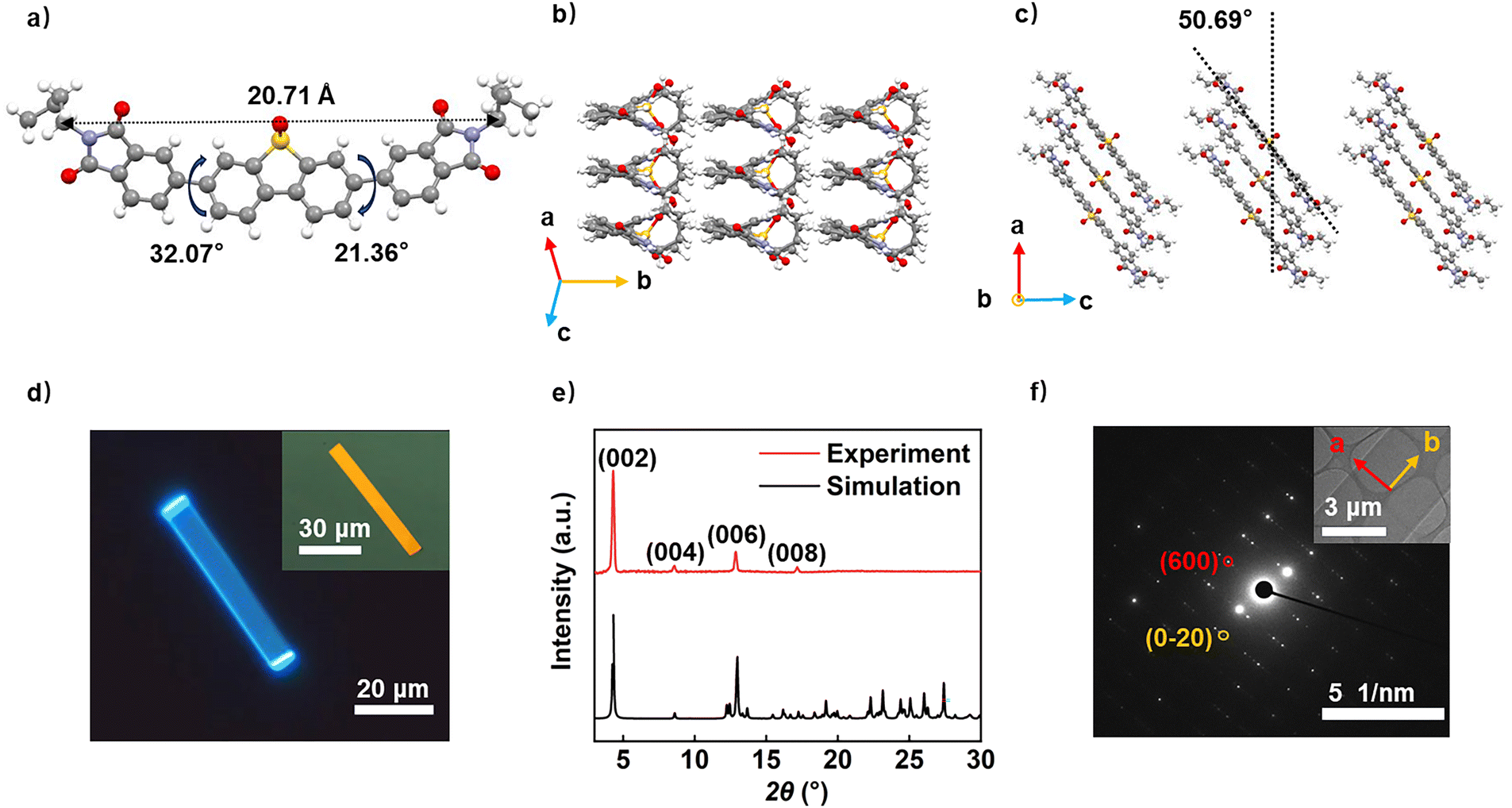 | ||
| Fig. 2 (a) Top view of a single DPIDBSO molecule. (b) and (c) Crystal packing structure of DPIDBSO. (d) Fluorescence image of an individual DPIDBSO crystal (inset: optical image of DPIDBSO crystal). (e) XRD pattern of the DPIDBSO microcrystal. (f) Selected area electron diffraction (SAED) of the DPIDBSO crystal (inset: corresponding TEM image). | ||
To elucidate this counterintuitive growth behaviour, we systematically analysed the interaction networks. Multiple weak hydrogen bonds were present between the adjacent molecules (Fig. 3a). These abundant intermolecular interactions could provide a substantial driving force for anisotropic crystal growth. Further investigation of molecular packing morphology revealed distinct surface characteristics along different crystallographic distinct surface characteristics along different crystallographic planes.37 The (200) and (−200) planes exhibited a slanted molecular arrangement with significant surface roughness at the molecular scale, which hindered crystal growth owing to the additional requirement for molecular orientation adjustment (Fig. 3b).38 In other words, a crystal growth dead zone existed along the a-axis direction. In contrast, the (010) and (0−10) planes demonstrated relatively smooth molecular terraces with reduced surface roughness, leading to easy prolongation along the b-axis (Fig. 3c).39
 | ||
| Fig. 3 (a) Illustration of multiple weak hydrogen bonds between molecules. (b) Molecular packing on (−200) and (200) faces. (c) Molecular packing on (0−10) and (010) faces. (d) Crystal growth process of DPIDBSO. | ||
Therefore, the synergistic effect of abundant weak hydrogen bond networks and favourable surface thermodynamics (Fig. 3d) resulted in observed growth anisotropy in the DPIDBSO crystals. These findings highlight the critical role of multiple non-covalent interactions in controlling crystal growth, challenging conventional assumptions about the dominance of π–π interactions in molecular crystal engineering.
To investigate the electrical properties of DPIDBSO, based on DPIDBSO microcrystals, we constructed field-effect devices with symmetrical gold electrodes and Ag electrodes (Fig. S6, ESI†). First, the conducting channel of the devices was set along the a-axis with a purpose, and these devices exhibited only n-type transport, achieving a maximum electron mobility of 0.02 cm2 V−1 s−1 among 15 devices (Fig. 4b). Considering the large injection barrier between the Au electrodes (work function: 5.1 eV) and DPIDBSO, we optimized the electrodes by employing Ag electrodes, which were better matched between the LUMO of DPIDBSO and the work function of the electrodes (Fig. 4a). This modification resulted in an enhancement of electron mobility to 0.07 cm2 V−1 s−1 (Fig. S7 and S8, ESI†) at a reduced source-drain voltage (Fig. 4c). Meanwhile, the onset of output curves in devices with silver electrodes occurred closer to 0 V, implying improved carrier injection. Moreover, we fabricated devices with channels along the b-axis to evaluate anisotropic transport (Fig. S9 and Table S3, ESI†). These devices with Au or Ag electrodes demonstrated higher electron mobility than that obtained in corresponding devices with channel oriented along the a-axis, yielding mobility of 0.13 cm2 V−1 s−1and 0.17 cm2 V−1 s−1, respectively (Fig. S10 and S11, ESI†). We ascribed such an unexpected increase in mobility to an obvious short-channel effect in devices along a-axis.40,41 Although the carrier injection was improved in devices with transferred silver electrodes, the output curve seems to be non-ideal. To achieve better contact, devices with evaporated silver electrodes were also fabricated, and these devices displayed similar transfer curves but more ideal output curves, regardless of the direction of the conducting channel (Fig. S12, ESI†). Finally, we measured the electroluminescence (EL) behaviour of DPIDBSO-based OLETs, which utilized only symmetric Ag electrodes. In devices oriented along the a-axis, although the mobility was slightly lower, clear electroluminescence was observed with an unmovable emission zone near the drain electrodes. The EL spectrum exhibited a peak at 496 nm, similar to the photoluminescence spectra (Fig. 4d). The EQE was calculated based on collected photocurrent curves, and the obtained maximal EQE was 0.24% (Fig. 4e and Fig. S13, ESI†). These results elucidate that DPIDBSO is a suitable material for fabricating n-type unipolar OLETs. As illustrated in Fig. 4f, in such unipolar OLETs, an electron accumulation layer was formed in the channel acting as a cathode, while holes were injected from one electrode functioning as an anode, thus leading to electroluminescence, similar to the operation of organic light-emitting diodes.42
 | ||
| Fig. 4 (a) Schematic of energy levels in OLETs. (b) Typical transfer curves of DPIDBSO-based devices with Au electrodes. (c) Typical transfer curves of DPIDBSO-based devices with Ag electrodes. (d) Electroluminescence spectra of DPIDBSO-based devices with Ag electrodes for the n-channel. (e) Typical transfer curves and EQE of DPIDBSO devices based on Ag electrodes for the n-channel. (f) Electroluminescence mechanism of DPIDBSO-based unipolar OLETs. | ||
Conclusions
In this study, we synthesized a dibenzothiophene sulfone-based n-type emissive organic semiconductor, DPIDBSO. Optical characterizations revealed that DPIDBSO was a blue-green emissive material with a PLQY of 30% in a solid state and a fast radiative decay rate. Surprisingly, we found that the growth direction of the DPIDBSO crystal did not align with the typical π–π stacking direction observed in other organic semiconductors, while its direction was consistent with the short axis of the molecule. This phenomenon was attributed to the presence of multiple weak hydrogen bonds and the differing rugosity of different crystal facets. Furthermore, DPIDBSO-based devices exhibited n-type transport, reaching electron mobility of 0.17 cm2 V−1 s−1, and more impressively, devices with Ag electrodes displayed clear electroluminescence, with an emission peak at 496 nm and EQE of 0.24%, demonstrating the feasibility of constructing n-type unipolar OLET devices. Our work highlights the potential of molecular design in advancing the development of high-performance n-type emissive organic semiconductors and offers guidance for the achievement of high-efficiency unipolar OLET devices.Author contributions
H. D. conceived this project, and Q. L. and S. Z. gave constructive feedback. X. C. and Q. L. performed the experiments and analysed the data. Y. L. provided help with crystallography measurements. S. G., P. W., Z. X., and D. L. performed the single crystal analysis. C. G., X. T. and M. S. helped with the OLET characterizations. All the authors discussed the results and commented on the manuscript.Data availability
The data supporting this article have been included as part of the ESI.†Conflicts of interest
There are no conflicts to declare.Acknowledgements
The authors acknowledge the financial support from the Ministry of Science and Technology of China (2022YFB3603800), the National Natural Science Foundation of China (52233010 and 52473203), Beijing National Laboratory for Molecular Sciences (BNLMS-CXXM-202012), and the CAS Project for Young Scientists in Basic Research (YSBR-053).Notes and references
- L. Zhao, J. Li, L. Li and W. Hu, J. Mater. Chem. C, 2024, 12, 13745–13761 RSC.
- Z. Qin, H. Gao, H. Dong and W. Hu, Adv. Mater., 2021, 33, e2007149 CrossRef.
- C. Zhang, P. Chen and W. Hu, Small, 2016, 12, 1252–1294 CrossRef CAS PubMed.
- M. U. Chaudhry, K. Muhieddine, R. Wawrzinek, J. Sobus, K. Tandy, S. C. Lo and E. B. Namdas, Adv. Funct. Mater., 2020, 30, 1905282 CrossRef CAS.
- Z. Wu, Y. Liu, E. Guo, G. Darbandy, S. J. Wang, R. Hubner, A. Kloes, H. Kleemann and K. Leo, Nat. Mater., 2021, 20, 1007–1014 CrossRef CAS.
- Z. Qin, C. Gao, H. Gao, T. Wang, H. Dong and W. Hu, Sci. Adv., 2022, 8, eabp8775 CrossRef CAS PubMed.
- B. Walker, M. Ullah, G. J. Chae, P. L. Burn, S. Cho, J. Y. Kim, E. B. Namdas and J. H. Seo, Appl. Phys. Lett., 2014, 105, 183302 CrossRef.
- R. Capelli, S. Toffanin, G. Generali, H. Usta, A. Facchetti and M. Muccini, Nat. Mater., 2010, 9, 496–503 CrossRef CAS PubMed.
- S. Z. Bisri, T. Takenobu and Y. Iwasa, J. Mater. Chem. C, 2014, 2, 2827–2836 RSC.
- J. Tao, D. Liu, J. Jing, H. Dong, L. Liu, B. Xu and W. Tian, Adv. Mater., 2021, 33, 2105466 CrossRef CAS PubMed.
- J. Li, L. Zheng, L. Sun, C. Li, X. Zhang, S. Cheng and W. Hu, J. Mater. Chem. C, 2018, 6, 13257–13260 RSC.
- D. Yuan, M. A. Awais, V. Sharapov, X. Liu, A. Neshchadin, W. Chen and L. Yu, J. Am. Chem. Soc., 2021, 143, 5239–5246 CrossRef CAS.
- L. Liu, C. Cai, Z. Zhang, S. Zhang, J. Deng, B. Yang, C. Gu and Y. Ma, ACS Mater. Lett., 2021, 3, 428–432 CrossRef CAS.
- M. Melucci, M. Durso, C. Bettini, M. Gazzano, L. Maini, S. Toffanin, S. Cavallini, M. Cavallini, D. Gentili, V. Biondo, G. Generali, F. Gallino, R. Capelli and M. Muccini, J. Mater. Chem. C, 2014, 2, 3448–3456 RSC.
- J. Liu, H. Zhang, H. Dong, L. Meng, L. Jiang, L. Jiang, Y. Wang, J. Yu, Y. Sun, W. Hu and A. J. Heeger, Nat. Commun., 2015, 6, 10032 CrossRef CAS PubMed.
- H. Ju, K. Wang, J. Zhang, H. Geng, Z. Liu, G. Zhang, Y. Zhao and D. Zhang, Chem. Mater., 2017, 29, 3580–3588 CrossRef CAS.
- J. Deng, Y. Xu, L. Liu, C. Feng, J. Tang, Y. Gao, Y. Wang, B. Yang, P. Lu, W. Yang and Y. Ma, Chem. Commun., 2016, 52, 2370–2373 RSC.
- J. Zhang, B. Xu, J. Chen, S. Ma, Y. Dong, L. Wang, B. Li, L. Ye and W. Tian, Adv. Mater., 2014, 26, 739–745 CrossRef.
- L. Bürgi, M. Turbiez, R. Pfeiffer, F. Bienewald, H.-J. Kirner and C. Winnewisser, Adv. Mater., 2008, 20, 2217–2224 CrossRef.
- L. Ma, D. Qin, Y. Liu and X. Zhan, J. Mater. Chem. C, 2018, 6, 535–540 RSC.
- L. Chen, Z. Qin, H. Huang, J. Zhang, Z. Yin, X. Yu, X. S. Zhang, C. Li, G. Zhang, M. Huang, H. Dong, Y. Yi, L. Jiang, H. Fu and D. Zhang, Adv. Sci., 2023, 10, e2300530 CrossRef.
- I. P. Koskin, C. S. Becker, A. A. Sonina, V. A. Trukhanov, N. A. Shumilov, A. D. Kuimov, Y. S. Zhuravleva, Y. O. Kiseleva, I. K. Shundrina, P. S. Sherin, D. Y. Paraschuk and M. S. Kazantsev, Adv. Funct. Mater., 2021, 31, 2104638 CrossRef CAS.
- Y. Zhang, Y. Wang, C. Gao, Z. Ni, X. Zhang, W. Hu and H. Dong, Chem. Soc. Rev., 2023, 52, 1331–1381 RSC.
- Y. Wan, J. Deng, W. Wu, J. Zhou, Q. Niu, H. Li, H. Yu, C. Gu and Y. Ma, ACS Appl. Mater. Interfaces, 2020, 12, 43976–43983 CrossRef CAS.
- Z. Qin, H. Gao, J. Liu, K. Zhou, J. Li, Y. Dang, L. Huang, H. Deng, X. Zhang, H. Dong and W. Hu, Adv. Mater., 2019, 31, e1903175 CrossRef PubMed.
- K. Niimi, H. Mori, E. Miyazaki, I. Osaka, H. Kakizoe, K. Takimiya and C. Adachi, Chem. Commun., 2012, 48, 5892–5894 RSC.
- J. Zaumseil, R. H. Friend and H. Sirringhaus, Nat. Mater., 2005, 5, 69–74 CrossRef.
- F. Reginato, E. Lunedei, S. Mattiello, G. Baroni, M. Bolognesi, F. Porcelli, G. Mattioli, Y. Hattori, M. Prosa, L. Beverina and S. Toffanin, Adv. Funct. Mater., 2025, 35, 2411845 CrossRef CAS.
- W. S. C. Roelofs, W. H. Adriaans, R. A. J. Janssen, M. Kemerink and D. M. de Leeuw, Adv. Funct. Mater., 2013, 23, 4133–4139 CrossRef CAS.
- P. Ganesan, H. N. Tsao and P. Gao, Adv. Funct. Mater., 2021, 31, 2105506 CrossRef CAS.
- B. Meng and J. Liu, Acc. Chem. Res., 2024, 57, 3478–3487 CrossRef CAS PubMed.
- T. Duan, J. Wang, W. Shi, Y. Li, K. Tu, X. Bi, C. Zhong, J. Lv, K. Yang, Z. Xiao, B. Kan and Y. Zhao, Angew. Chem., Int. Ed., 2024, 63, e202407890 CrossRef CAS.
- L. Yuan, Y. Huang, X. Chen, Y. Gao, X. Ma, Z. Wang, Y. Hu, J. He, C. Han, J. Li, Z. Li, X. Weng, R. Huang, Y. Cui, L. Li and W. Hu, Nat. Mater., 2024, 23, 1268–1275 CrossRef CAS PubMed.
- Q. Li, Y. Zhang, J. Lin, Y. Zou, P. Wang, Z. Qin, Y. Wang, Y. Li, Y. Zhang, C. Gao, Y. Zang, W. Hu and H. Dong, Angew. Chem., Int. Ed., 2023, 62, e202308146 CrossRef CAS PubMed.
- Y. Xu, P. Xu, D. Hu and Y. Ma, Chem. Soc. Rev., 2021, 50, 1030–1069 RSC.
- M. Li, Y. Liu, R. Duan, X. Wei, Y. Yi, Y. Wang and C. F. Chen, Angew. Chem., Int. Ed., 2017, 129, 8944–8948 CrossRef.
- R. Montis, R. J. Davey, S. E. Wright, G. R. Woollam and A. J. Cruz-Cabeza, Angew. Chem., Int. Ed., 2020, 59, 20357–20360 CrossRef CAS.
- Y. Liu, J. F. B. Black, K. F. Boon, A. J. Cruz-Cabeza, R. J. Davey, R. J. Dowling, N. George, A. Hutchinson and R. Montis, Cryst. Growth Des., 2019, 19, 4579–4587 CrossRef CAS.
- Y. Liu, B. Gabriele, R. J. Davey and A. J. Cruz-Cabeza, J. Am. Chem. Soc., 2020, 142, 6682–6689 CrossRef CAS PubMed.
- J. N. Haddock, X. Zhang, S. Zheng, Q. Zhang, S. R. Marder and B. Kippelen, Org. Electron., 2006, 7, 45–54 CrossRef.
- B. Peng, K. Cao, A. H. Y. Lau, M. Chen, Y. Lu and P. K. L. Chan, Adv. Mater., 2020, 32, e2002281 CrossRef.
- J. S. Swensen, C. Soci and A. J. Heeger, Appl. Phys. Lett., 2005, 87, 253511 CrossRef.
Footnotes |
| † Electronic supplementary information (ESI) available. CCDC 2428822. For ESI and crystallographic data in CIF or other electronic format see DOI: https://doi.org/10.1039/d5tc00969c |
| ‡ These contributed equally to this work. |
| This journal is © The Royal Society of Chemistry 2025 |