Flexible unipolar thermoelectric devices based on patterned poly[Kx(Ni-ethylenetetrathiolate)] thin films†
Liyao
Liu
ab,
Yuanhui
Sun
a,
Wenbo
Li
a,
Jiajia
Zhang
ab,
Xing
Huang
ab,
Zhijun
Chen
ab,
Yimeng
Sun
a,
Chongan
Di
*a,
Wei
Xu
 *ab and
Daoben
Zhu
 *ab
*ab
aBeijng National Laboratory for Molecular Science, Institute of Chemistry, Chinese Academy of Sciences, Beijing, 100190, China. E-mail: wxu@iccas.ac.cn; dicha@iccas.ac.cn; zhudb@iccas.ac.cn
bUniversity of Chinese Academy of Science, Beijing, 100190, China
First published on 18th July 2017
Abstract
By printing polydimethylsiloxane (PDMS) on a polyethylene terephthalate (PET) substrate as a mask, an insoluble and infusible metal coordination polymer, poly[Kx(Ni-ethylenetetrathiolate)] (poly[Kx(Ni-ett)]), film was patterned via an electrochemical deposition process. The method is verified to be capable of fabricating 108 n-type legs in one batch. A thermoelectric generator consisting of eighteen legs connected in series in one row had an output power of 0.468 μW under a temperature difference of 12 K with the best power density reaching up to 577.8 μW cm−2.
Introduction
Driven by the current energy and environmental issues, thermoelectric generators (TEGs) have attracted growing attention as they provided a green pathway to convert thermal energy into electricity and vice versa.1,2 So far, thermoelectric devices based on inorganic semiconductors have already been commercialized, while the non-flexibility and scarcity of inorganic materials and the non-scalable manufacturing techniques definitely hinder these devices from being widely employed in daily life.3 Very recently, thermoelectric devices based on organic materials have shown great potential for energy harvesting or cooling in a low temperature range.4 Moreover, organic thermoelectric materials (OTEs) have many advantages such as flexibility, light weight, solution processability, low cost and abundant resources.5 Thus, OTEs are more suitable to be integrated as power supply units into self-powered wearable electronics and medical sensors compared to their inorganic counterparts.6,7 The efficiency of a thermoelectric material is determined by its dimensionless figure of merit, ZT = S2σT/κ, where S is the Seebeck coefficient, σ is the electrical conductivity, κ is the thermal conductivity including contributions from both phonons (κL) and electrons (κe) and T is the absolute temperature.8 Until now, the highest ZT values reported for OTEs have been 0.42 (p-type) in PEDOT:PSS9 and 0.30 ± 0.03 (n-type)10 in coordination polymers, e.g. poly[Kx(Ni-ethylenetetrathiolate)] (poly[Kx(Ni-ett)]), at room temperature, respectively.In the past several years, there have been ongoing efforts to synthesize n-type thermoelectric materials based on poly[Kx(Ni-ett)]. In the year 2012, Sun et al.11 reported TE properties of coordination polymers with a general formula of poly[Ax(M-ett)] (A = K or Cu, M = Ni or Cu), which displayed tunable charge carrier species by varying the metal ions. In particular, poly[Kx(Ni-ett)] showed a ZT value of 0.2 at 440 K, which was the best n-type OTE ever reported at that time. A bulk TE device composed of 35 n–p couples based on n-type poly[Kx(Ni-ett)] and p-type poly[Cux(Cu-ett)] showing a power output of 750 μW (under a temperature gradient of 82 K) demonstrated the great potential of OTEs for practical application. And after that, Sheng et al.12 employed a molding method to fabricate TEGs containing 220 pairs of thermocouples composed of ett based coordination polymers. The maximum power output exceeded 1.0 mW, which was the highest performance ever reported for OTE devices. However, the insoluble and infusible nature of the materials mentioned above makes them unsuitable for traditional solution fabrication procedures, such as solution casting, spin coating or jet printing, which will limit their applications. In order to overcome this obstacle, it’s essential to develop scalable and cost-effective manufacturing methods to fabricate flexible thermoelectric devices to meet the emerging demands for wearable electronics.13 In an earlier attempt, Jiao et al.14 successfully dispersed poly[Ax(M-ett)] with polyvinylidene fluoride (PVDF) in DMSO to form a printable ink to fabricate flexible TEGs on polyethylene terephthalate (PET) substrates via jet printing. Regretfully, the composite materials formed from PVDF and poly[Ax(M-ett)] particles displayed an obvious reduction in electrical conductivity compared to that of pristine poly[Ax(M-ett)]. Thus, finding an optimized method to improve the processability of poly[Kx(Ni-ett)] and to maintain its original high performance is in high demand. Very recently, Sun et al.10 developed an electrochemical method to deposit thin films of poly[Kx(Ni-ett)] on a series of flexible insulating substrates. This is the latest progress towards the fabrication of flexible OTE generators based on this coordination polymer through a low cost wet-chemistry process. A significant enhancement of TE performance was achieved simultaneously with the highest ZT value of up to 0.30 ± 0.03 at room temperature for this n-type OTE material. However, getting poly[Kx(Ni-ett)] integrated into flexible TEG devices will remain a challenge until we can find a facile way to pattern its thin films with suitable dimensionality.
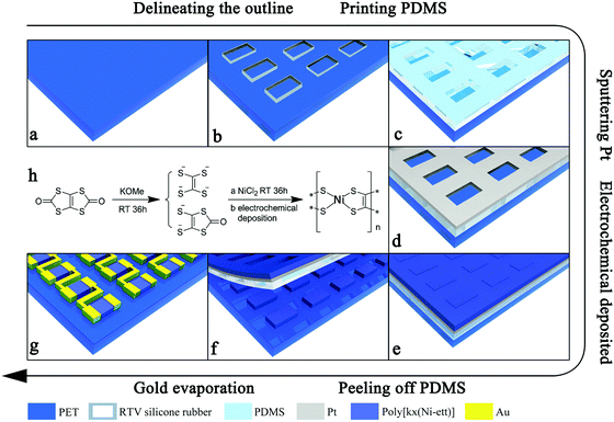
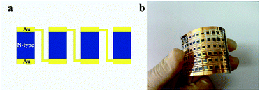
Here, employing a prepatterned polyethylene terephthalate (PET) substrate, an insoluble and infusible metal coordination polymer, poly[Kx(Ni-ethylenetetrathiolate)] (poly[Kx(Ni-ett)]), film was patterned via an electrochemical deposition process (illustrated in Scheme 1). Arrays of poly[Kx(Ni-ett)] bars (each bar has a size of 1.5 × 2.5 mm2) could be obtained by this method, and they can be further connected in series to form a prototype unipolar TEG. The device not only maintained the promising TE properties of original materials but also demonstrated an improvement in processability. This strategy could be extended to other polymer-based TE materials with electrochemical activities to make them suitable to be patterned and processed for the fabrication of flexible TE devices.
Experimental
Materials
1,3,4,6-Tetrathiapentalene-2,5-dione (TPD; Tci, 98%), nickel(II) chloride (Alfa Aesar, 99%), dry methanol (Acros, extra dry, 99.8%), potassium methoxide (Adamas beta, 98%), polydimethylsiloxane (PDMS, Dow corning sylgard 184), room temperature vulcanized (RTV) silicone rubber (Dow corning 3145), and polyethylene glycol terephthalate (PET) substrates were used as received.Methods
Next, a thin layer of Pt metal (with a thickness of 4–20 nm) was sputtered (via SCD 500, LeicaEM) onto the surface of the PDMS layer through a shadow mask leaving the pre-patterned rectangles uncovered (Scheme 1d). According to our previous observation, during the electrochemical deposition process, the poly[Kx(Ni-ett)] film spread from the edge of the electrode to cover the whole surface of the polymer substrate attached to the electrode. Here, the sputtered Pt film served as the electrode to ensure that each rectangle area was covered with the poly[Kx(Ni-ett)] film uniformly.
After removing the PDMS mask, only poly[Kx(Ni-ett)] films in direct contact with PET were left on the substrate (as shown in Fig. S1a, ESI†), which finally led to the formation of poly[Kx(Ni-ett)] arrays of 6 × 18 rectangular bars in one batch with each bar having an approximate dimension of 1.5 × 2.5 mm2 (Scheme 1g).
Results and discussion
In a previous work, we have shown that poly[Kx(Ni-ett)] films exhibited different adhesive abilities towards polymer substrates in the order Teflon < PI < PET. So, a PET substrate is the best one for further device fabrication. To accomplish device fabrication, we should find an efficient way to pattern the poly[Kx(Ni-ett)] films.15–17 A series of pattern methods have been investigated, such as laser photoetching, plasma etching and so on. Obviously, laser photoetching was infeasible for such a polymer substrate supported thin film, as the PET substrate wrinkled under the high temperature generated by the laser. Besides, poly[Kx(Ni-ett)] films showed great resistance towards the oxygen plasma. Finally, we designed a practicable and low-cost process to deposit poly[Kx(Ni-ett)] arrays on pre-patterned PET substrates, as illustrated in Scheme 1. For device fabrication, gold was chosen as the electrode material considering energy-matching and efficient electron injection and collection, as poly[Kx(Ni-ett)] is a degenerate-semiconductor material with a work function of 4.52 eV which matched well with the work function of the Au electrode after air-exposure (4.7 eV).10,18 Moreover, in a series of previous works on poly[Kx(Ni-ett)] TE materials, gold electrodes were employed for device fabrication, by which the fabricated TEG devices showed good performance and robust stability.11,12,14 Employing this approach, a flexible unipolar device composed of 18 n-type poly[Kx(Ni-ett)] legs connected in series (each leg has a size of 1.5 × 2.5 × 0.003 mm3) was fabricated on a PET substrate.In principle, TEGs should be fabricated by combining both p-type and n-type TE materials for achieving high efficiency. Presently, most of the efficient polymer based TE materials that are solution processable and suitable for flexible device fabrication are PEDOT derivatives or its analogues,19,20 which means that they are p-type materials. However, the performance of solution processable n-type OTEs significantly lags behind those of p-type materials. This situation will heavily hinder the practical application of OTEs. Currently, ploy(Ni-ett) is the only n-type OTE possessing a ZT value comparable to those of PEDOT based OTEs. Making this material solution processable without sacrificing its performance is critical for the development of OTEs. Here, the fabrication of a unipolar device based on ploy(Ni-ett) thin films will demonstrate that the electrochemical deposition procedure is a feasible, low cost wet-chemistry method for patterning organic OTEs that is comparable to the conventional solution processing methods such as spin casting or ink-printing. A prototype device containing 18 thermoelectric legs was fabricated by linking the poly(Ni-ett) array in one row in a head-to-tail manner, which was investigated and found to convert thermal gradient into electricity along the in-plane direction. Obviously, the size and density of the poly(Ni-ett) arrays could be easily adjusted by tuning the PDMS mask, and devices with one row of the poly(Ni-ett) array can be further connected in series or parallel to improve their output power performance.
First, TE performance of the individual legs was characterized with emphasis laid on the consistency among each other. A Seebeck voltage (ΔU) could be measured between two ends of the leg along with the corresponding temperature difference (ΔT). Fig. 3 illustrates the performance distribution of the patterned poly(Ni-ett) thin films including the Seebeck coefficient (S = ΔU/ΔT), conductivity and power factor (PF = S2σ). One-fifth of the legs (n = 22) on one substrate were randomly chosen for testing. The Seebeck coefficient and conductivity measured by two probes were approximately normally distributed, which mainly concentrated in the range −100 to −120 μV K−1 and 192.5–252.5 S cm−1, respectively. Consequently, a power factor ranging from 155 to 200 μW m−1 K−2 was calculated. These results indicate that the performance of each element on the same substrate is highly consistent with each other, which is critical for the integration and mass production of the devices. Nevertheless, the difference in the performance of devices deposited on different substrates is relatively larger, which is mainly due to the variation in films' quality.10
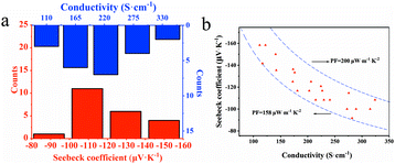 | ||
| Fig. 3 Performance distribution for a typical poly[Kx(Ni-ett)] film, (a) the range of Seebeck coefficient and conductivity and (b) power factor. | ||
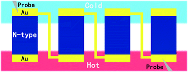
Two Pielter devices were employed to generate a temperature gradient across the testing device. At ΔT = 12 K, which comes closer to the realistic temperature gradient between the ambient environment and human body, an eighteen-leg thermoelectric device exhibits a maximum output power of 0.468 μW with an open voltage of 25.66 mV and a short-circuit current of 72.98 μA as shown in Fig. 4a. Under this condition, the Seebeck coefficient of the single N-leg device is 118.8 μV K−1 by dividing the open voltage (25.66 mV) with the number of legs (18) and temperature difference (12 K), which is consistent with the measured results shown in Fig. 3. To further evaluate the total TE output power of the fabricated TEG, we measured its open-circuit voltage and short-circuit current as a function of the temperature difference, as shown in Fig. 4b. Voc and ISC increase nearly linearly with the temperature difference. The dependence of maximum output power tendency towards the temperature difference is also shown in Fig. 4b. It can be seen that Pmax increased with ΔT proportionally to the square of Voc, as expected from the theoretical formula for the maximum output power mentioned above. The relatively low power output of the eighteen-leg poly[Kx(Ni-ett)] TE device is due to the thinness of the film as well as the electrical contact resistance, thus affecting the internal resistance of the generator. The maximum power density of one leg is 577.8 μW cm−2 with an average value of 300.3 μW cm−2, which is the best performance ever reported for poly[Kx(Ni-ett)] based TEGs. Here, for comparison with a conventional bulk device with vertically aligned TE legs, the power density (PD) of this thin film device was estimated by dividing the power output with the cross-sectional area of the thin film along the perpendicular direction of temperature gradient (PD = Pmax/NSc, where N is the number of legs, Sc is the cross-sectional area).21
A number of studies have been done to enhance the performance of poly[Kx(Ni-ett)] materials. Table 1 summarizes the device fabrication methods and TEG performance results based on poly[Kx(Ni-ett)] ever reported. A TEG with a larger temperature gradient, more n–p couples and a lower inner resistance tends to produce more power output. It can be explained by another formula of the maximum output power (Pmax = N(SΔT)2/4R), where N is the number of legs, ΔT is the temperature gradient and R represents the inner resistance including the original resistance of materials as well as the contact resistance and electrode resistance.4 What’s more, synthesizing a thicker film can help reduce the original resistance of thermoelectric materials, which will further affect the performance of TEGs. So power density is calculated for better comparison of materials and device performance. The maximum power density of poly[Kx(Ni-ett)] is thirteen times larger than that of the best material reported (107.1 μW cm−2) in the literature,11 while the average power density is five times more than its value. However, materials of that article are powdered samples, the structure-ordering characteristic of which hinders the electrical conductivity compared with thin films.22–24 Besides, the highest power density of the poly[Kx(Ni-ett)] film device reported previously was 15.3 μW cm−2. It's worth noting that the present work has improved this property of poly[Kx(Ni-ett)] film devices by one or two orders of magnitude.
| Methods | Materials | S* (mm2) | D (μm) | N | ΔT (K) | P max (μW) | Cross-sectional area (mm2) | PD (μW cm−2) | Ref. | |
|---|---|---|---|---|---|---|---|---|---|---|
| n-Type | p-Type | |||||||||
| S*, D, N, ΔT, P and PD stand for, respectively, the size, thickness of each device, number of TE legs, temperature gradient, maximum power output, and power density of each device. | ||||||||||
| Powder compact | Poly[Kx(Ni-ett)] | Poly[Cux(Cu-ett)] | 5 × 2 | 900 | 35 × 2 | 82 | 750 | 5 × 2 | 107.1 | 11 |
| Molding | Poly[Kx(Ni-ett)] | Cu(I)-ett | 2 × 1 | 5000 | 220 × 2 | 60 | 1000 | 5 × 2 | 22.7 | 12 |
| Inkjet printing | Poly[Kx(Ni-ett)]/PVDF | Poly[Cux(Cu-ett)]/PVDF | 5 × 3 | 2–5 | 6 × 2 | 50 | 0.011 | 3 × (2–5) × 10−3 | 6.1–15.3 | 14 |
| Printing and electrochemistry | Poly[Kx(Ni-ett)] | — | 2.5 × 1.5 | 3 | 18 | 12 | 0.468 | 1.5 × 3 × 10−3 | 577.8 | This work |
The electrochemistry process allows us to synthesize pure poly[Kx(Ni-ett)] films without the insulating PVDF composited. An average Seebeck coefficient of −153.26 μV K−1 for 108 legs can be calculated from the dependence of open-circuit output voltage on temperature difference, which coincides with the previous report.10 However, the electrical conductivity slightly decreases. The major limitation of this device is the larger contact resistance compared to that of the electrical resistance of poly[Kx(Ni-ett)] itself, which has a negative impact on the output power.25,26
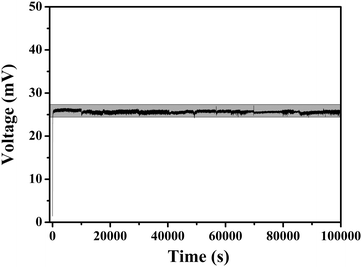
Long-term operation stability under atmospheric conditions is essential for practical applications, which is monitored by measuring the Seebeck voltage (ΔU) with the corresponding length of time under an ambient atmosphere. The poly[Kx(Ni-ett)] film devices exhibit excellent stability, as demonstrated by their steady output voltage response to a temperature difference of 12 K. The device does not show any observable degeneration after operating for 105 seconds under an ambient atmosphere (Fig. 5).
Conclusions
In summary, we have demonstrated a method for patterning insoluble and infusible materials to fabricate TE devices on flexible polymer substrates, which has advantages in terms of facility, flexibility, low cost and solution processability. Specifically, a poly[Kx(Ni-ett)] film is patterned via an electrochemical process on a prepatterned PET substrate with a printed PDMS layer serving as a mask. The highest power density of a device containing eighteen legs reaches 577.8 μW cm−2 under a temperature gradient of 12 K, which is the best performance ever reported for thermoelectric devices based on this material. Notably, this manufacturing technique will have extensive application prospects.Acknowledgements
The authors acknowledge the financial support from the Chinese Ministry of Science and Technology (2013CB632506), the Strategic Priority Research Program of the Chinese Academy of Sciences (Grant No. XDB12000000), and the National Natural Science Foundation of China (21333011).Notes and references
- B. Russ, A. Glaudell, J. J. Urban, M. L. Chabinyc and R. A. Segalman, Nat. Rev. Mater., 2016, 1, 16050 CrossRef CAS.
- L. E. Bell, Science, 2008, 321, 1457–1461 CrossRef CAS PubMed.
- Q. Zhang, Y. Sun, W. Xu and D. Zhu, Adv. Mater., 2014, 26, 6829–6851 CrossRef CAS PubMed.
- O. Bubnova, Z. U. Khan, A. Malti, S. Braun, M. Fahlman, M. Berggren and X. Crispin, Nat. Mater., 2011, 10, 429–433 CrossRef CAS PubMed.
- A. C. Arias, J. D. MacKenzie, I. McCulloch, J. Rivnay and A. Salleo, Chem. Rev., 2010, 110, 3–24 CrossRef CAS PubMed.
- J.-H. Bahk, H. Fang, K. Yazawa and A. Shakouri, J. Mater. Chem. C, 2015, 3, 10362–10374 RSC.
- G. Schwartz, B. C. K. Tee, J. G. Mei, A. L. Appleton, D. H. Kim, H. L. Wang and Z. N. Bao, Nat. Commun., 2013, 4, 1859 CrossRef PubMed.
- R. Venkatasubramanian, E. Siivola, T. Colpitts and B. O'Quinn, Nature, 2001, 413, 597–602 CrossRef CAS PubMed.
- G.-H. Kim, L. Shao, K. Zhang and K. P. Pipe, Nat. Mater., 2013, 12, 719–723 CrossRef CAS PubMed.
- Y. Sun, L. Qiu, L. Tang, H. Geng, H. Wang, F. Zhang, D. Huang, W. Xu, P. Yue, Y. S. Guan, F. Jiao, Y. Sun, D. Tang, C. A. Di, Y. Yi and D. Zhu, Adv. Mater., 2016, 28, 3351–3358 CrossRef CAS PubMed.
- Y. Sun, P. Sheng, C. Di, F. Jiao, W. Xu, D. Qiu and D. Zhu, Adv. Mater., 2012, 24, 932–937 CrossRef CAS PubMed.
- P. Sheng, Y. Sun, F. Jiao, C. Di, W. Xu and D. Zhu, Synth. Met., 2014, 193, 1–7 CrossRef CAS.
- M. Zebarjadi, K. Esfarjani, M. S. Dresselhaus, Z. F. Ren and G. Chen, Energy Environ. Sci., 2012, 5, 5147–5162 Search PubMed.
- F. Jiao, C. A. Di, Y. Sun, P. Sheng, W. Xu and D. Zhu, Philos. Trans. R. Soc., A, 2014, 372, 20130008 CrossRef PubMed.
- R. Srinivasan, Science, 1986, 234, 559–565 CAS.
- Y. Yang, D. K. Taggart, M. H. Cheng, J. C. Hemminger and R. M. Penner, J. Phys. Chem. Lett., 2010, 1, 3004–3011 CrossRef CAS.
- G. Pennelli, M. Totaro, M. Piotto and P. Bruschi, Nano Lett., 2013, 13, 2592–2597 CrossRef CAS PubMed.
- H. Lee, Y. Zhang, L. Zhang, T. Mirabito, E. K. Burnett, S. Trahan, A. R. Mohebbi, S. C. B. Mannsfeld, F. Wudl and A. L. Briseno, J. Mater. Chem. C, 2014, 2, 3361–3366 RSC.
- W. Lee, M. Song, S. Park, S. Nam, J. Seo, H. Kim and Y. Kim, Sci. Rep., 2016, 6, 33795 CrossRef CAS PubMed.
- C. Cho, K. L. Wallace, P. Tzeng, J.-H. Hsu, C. Yu and J. C. Grunlan, Adv. Energy Mater., 2016, 6, 1502168 CrossRef.
- F. Huewe, A. Steeger, K. Kostova, L. Burroughs, I. Bauer, P. Strohriegl, V. Dimitrov, S. Woodward and J. Pflaum, Adv. Mater., 2017, 29, 1605682 CrossRef PubMed.
- W. B. Chang, H. Y. Fang, J. Liu, C. M. Evans, B. Russ, B. C. Popere, S. N. Patel, M. L. Chabinyc and R. A. Segalman, ACS Macro Lett., 2016, 5, 455–459 CrossRef CAS.
- W. B. Chang, C. M. Evans, B. C. Popere, B. M. Russ, J. Liu, J. Newman and R. A. Segalman, ACS Macro Lett., 2016, 5, 94–98 CrossRef CAS.
- W. B. Chang, H. Fang, J. Liu, C. M. Evans, B. Russ, B. C. Popere, S. N. Patel, M. L. Chabinyc and R. A. Segalman, ACS Macro Lett., 2016, 5, 455–459 CrossRef CAS.
- S. L. Kim, K. Choi, A. Tazebay and C. Yu, ACS Nano, 2014, 8, 2377–2386 CrossRef CAS PubMed.
- C. A. Hewitt, D. S. Montgomery, R. L. Barbalace, R. D. Carlson and D. L. Carroll, J. Appl. Phys., 2014, 115, 184502 CrossRef.
Footnote |
| † Electronic supplementary information (ESI) available. See DOI: 10.1039/c7qm00223h |
| This journal is © the Partner Organisations 2017 |

