
 Open Access Article
 This Open Access Article is licensed under a
 Creative Commons Attribution 3.0 Unported Licence
Correction: Broadening spectral responses and achieving environmental stability in SnS2/Ag-NPs/HfO2 flexible phototransistors
Muhammad Farooq
Khan
a,
Sana
Sadaqat
b,
Muhammad Asghar
Khan
c,
Shania
Rehman
d,
Waqas Siddique
Subhani
e,
Mohamed
Ouladsmane
f,
Malik Abdul
Rehman
g,
Fida
Ali
h,
Harri
Lipsanen
h,
Zhipei
Sun
h,
Jonghwa
Eom
*c and
Faisal
Ahmed
*h
aDepartment of Electrical Engineering, Sejong University, Seoul 05006, Republic of Korea
bDepartment of Physics, Riphah International University, Faisalabad Campus, 44000, Pakistan
cDepartment of Physics and Astronomy, Sejong University, Seoul 05006, Republic of Korea. E-mail: eom@sejong.ac.kr
dDepartment of Semiconductor System Engineering, Sejong University, Seoul 05006, Republic of Korea
eDepartment of Physics, University of Lahore, Lahore, 53700, Pakistan
fDepartment of Chemistry, College of Science, King Saud University, Riyadh, 11451, Saudi Arabia
gDepartment of Chemical Engineering, New Uzbekistan University, Tashkent, 100007, Uzbekistan
hDepartment of Electronics and Nano Engineering, Aalto University, P.O. Box 13500, FI-00076 Aalto, Finland. E-mail: faisal.ahmed@aalto.fi
First published on 2nd December 2024
Abstract
Correction for ‘Broadening spectral responses and achieving environmental stability in SnS2/Ag-NPs/HfO2 flexible phototransistors’ by Muhammad Farooq Khan et al., Nanoscale, 2024, 16, 3622–3630, https://doi.org/10.1039/D3NR04626E.
The authors regret the use of the word nanoparticle or NP. The correct term is nanodot. Each instance of the term nanoparticle or NP should be read as nanodot. An expert has reviewed the usage and agreed that nanodot is the appropriate term.
The authors regret the omission of the Ag nanodot fabrication method in the original paper. An expert has reviewed the fabrication method and agreed it is consistent with the results presented.
The authors would also like to clarify why there are repetitive patterns in the SEM image in the Fig. 2a inset, of the original paper. The authors used AutoCAD software to design the nanodots on the SnS2 flake. They were patterned with electron beam lithography and the silver was deposited with a thermal evaporator. Nanodots of approximately 50 nm, 100 nm and 150 nm were patterned.
The following details the Ag nanodots fabrication on the SnS2 flake.
1. First, AutoCAD software was used to design patterns for Ag nanodots, as shown here in Fig. 1a. The appearance of repetitive patterns of nanodots observed in the SEM image is due to the intentional design followed.
 | ||
| Fig. 1 (a) AutoCAD design pattern used to fabricate the Ag dots. (b) and (c) are SEM images of the Fig. 2a inset of the original paper. | ||
2. The mechanically exfoliated SnS2 flake was coated with an electron beam resist, i.e., polymethyl methacrylate (PMMA).
3. The chips were baked at 170 °C for 2 minutes on a hot plate in the ambient environment.
3. Electron beam lithography was utilized to create the patterns of nanodots.
4. A ∼15 nm thick layer of Ag metal was deposited using a thermal evaporator in a vacuum chamber.
5. The flakes were rinsed with acetone and methanol to remove the excessive Ag metal and complete the lift-off process, resulting in Fig. 1b and c shown here.
Additional examples to show the reproducibility of the process are shown here in Fig. 2.
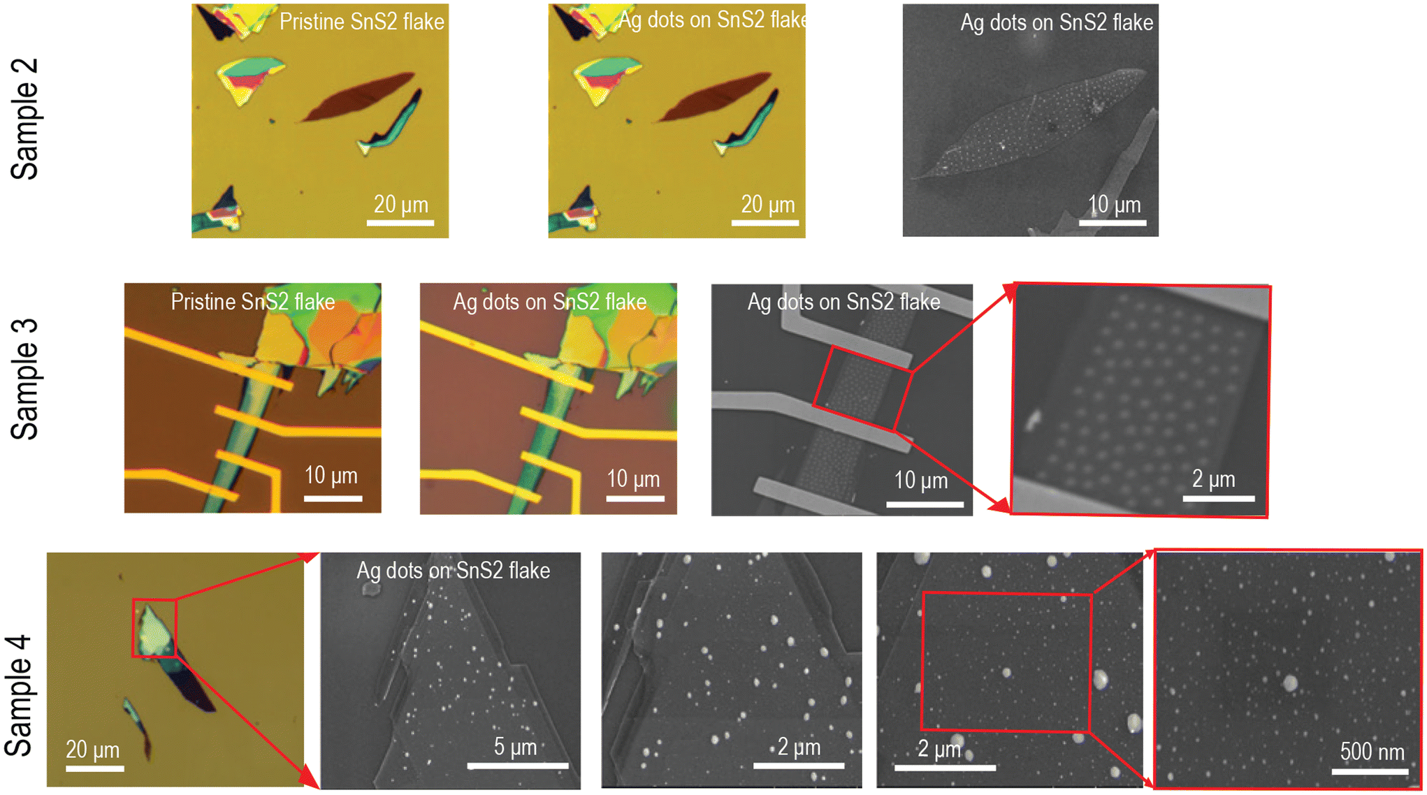 | ||
| Fig. 2 Optical micrographs and SEM images of three other SnS2 samples with Ag dots. | ||
The Royal Society of Chemistry apologises for these errors and any consequent inconvenience to authors and readers.
| This journal is © The Royal Society of Chemistry 2025 |