
 Open Access Article
 This Open Access Article is licensed under a Creative Commons Attribution-Non Commercial 3.0 Unported Licence
Deep-blue amplified spontaneous emission and lasing in colloidal silicon nanoclusters†
Hiroyuki Yamada a,
Tohru Tsuruoka*a,
Tadaaki Nagaoab and
Naoto Shirahata*ac
a,
Tohru Tsuruoka*a,
Tadaaki Nagaoab and
Naoto Shirahata*ac
aResearch Center for Materials Nanoarchitectonics (MANA), National Institute for Materials Science (NIMS), 1-1 Namiki, Tsukuba, 305-0044, Japan. E-mail: tsuruoka.tohru@nims.go.jp; shirahata.naoto@nims.go.jp
bGraduate School of Science, Hokkaido University, Sapporo 060-0810, Japan
cGraduate School of Chemical Sciences and Engineering, Hokkaido University, Sapporo 060-0814, Japan
First published on 14th April 2025
Abstract
We report for the first time the amplified spontaneous emission (ASE) and lasing from blue-emitting silicon nanoclusters. The lasing threshold is determined as 1.8 mJ per pulse and the emission peaks at 434 nm. The laser-induced emission experiments demonstrated in this study encourage further development of solution-processed fabrication of a colloidal silicon quantum dot laser.
Amplified spontaneous emission (ASE) in the blue region of the visible-spectral wavelength has attracted much interest owing to its potential use for various applications such as full-color lasers and their spectral superimposition for white lasers.1 Colloidal semiconductor quantum dots (CQDs) have been widely explored as optical gain media because of their characteristic stability against heat and light, along with the solution-processability of molecular compounds.2 A major obstacle of the CQDs is nonradiative carrier losses, which are caused by nonradiative Auger relaxation and recombination at surface traps or defects.3 The decrease in size of CQDs, which requires blue-light emission based on the quantum confinement effect, enhances the defect formation because of the increasing surface–volume ratio, resulting in an increase of the nonradiative Auger rate due to increasing Coulomb electron–electron coupling.4 Thus, the presence of the nonradiative recombination pathways retards the development of lasing at blue wavelengths. There have been several attempts to find a good optical gain medium. For example, nonspherical CQDs with tetrapod- or rod-shape structures have been reported to suppress Auger recombination rates.5 Organic–inorganic lead perovskite nanoclusters show large absorption coefficients and low defect densities;6 however their lack of high-thermal stability, ascribed to the organics that are constituents of the hybridized structures, limits their use for photonic applications. Alternatively, fully-inorganic perovskites have been proposed to overcome the poor stability against heat and light.7 Here, we report silicon nanoclusters as a new optical gain medium. Since Kauzlarich's pioneering work in 1999,8 various solution routes have been developed for the synthesis of blue-emitting silicon nanoclusters.9–11 In accordance with the protocol we reported,12 a wafer of silicon was ablated in 1-decene with a third-harmonic radiation of a Nd:YAG laser (see Fig. 1). As reported, the laser ablation produces silicon nanoclusters through the condensation and rapid quenching of the vapor of silicon generated by the ablation. In the absence of oxygen molecules and moisture, the surface of the nanoclusters remains covered with silicon-centered radicals. The terminal α-carbons of 1-decenes surrounding the resultant nanoclusters form covalent bonds between carbon and silicon, yielding decane-terminated silicon nanoclusters (see the ESI,† for details). Dispersion of the purified product in dichloromethane appeared transparent and very dilute pale-yellow to the naked eye. Fig. 1b shows a representative high-angle annular dark-field (HAADF) scanning transmission electron microscopy (STEM) image of the sample. As expected, the nanoclusters, which are contrasted as white dots due to the higher Z-contrast sensitivity of silicon than carbon in the 6-nm-thick amorphous carbon film covering the copper TEM grid, dispersed without aggregation all around. Such a high contrast observed suggests that the dots have a crystalline structure rather than an amorphous one.13 The diameters of these dots are close to or less than 1 nm, along with a narrow size-distribution. A typical bright field image is shown in Fig. 1c. Lattice fringes were clearly observed as indicated by the open-circles. In addition, the nanocluster surface was not amorphized but faceted, suggesting the appearance of an anchor effect of the decane-monolayers, which protects the surface from amorphization as reported previously for alkyl monolayers.14 Attenuated total reflection Fourier-transform infrared (ATR-FTIR) spectroscopy indicated the formation of a decane monolayer and partial oxidation of the nanocluster surface as shown in Fig. 1d (see Fig. S1, ESI†).
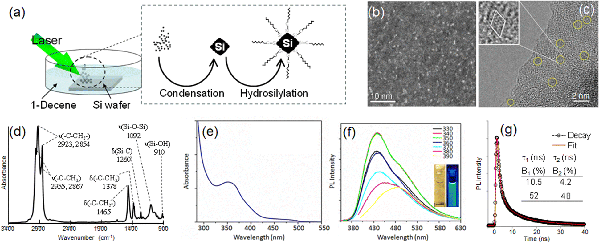 | ||
| Fig. 1 (a) A scheme for the synthesis of decane-terminated silicon nanocrystals. (b) HAADF-STEM image, (c) HR-TEM image, (d) ATR-FT-IR spectrum, (e) UV-vis absorption spectrum, (f) PL spectra at different excitations and (g) PL decay curve of the silicon nanocrystals. The inset of panel (f) shows the digital photographs of dichloromethane solution of the silicon nanocrystals under room illumination (left) and 365-nm UV lamp (right). In panel (g), the best fit was obtained by biexponential decay functions (χ2 = 1.12). | ||
The optical absorption spectrum shown in Fig. 1e exhibits similar characteristics to silicon nanoclusters emitting in the blue spectral region reported elsewhere in the literature.8,11,12 Fig. 1f shows PL spectra collected by varying the excitation wavelength from 330 nm to 390 nm in 10 nm increments. The inset shows digital photographs of the nanoclusters under room illumination (left) and UV (λem = 365 nm) light irradiation (right), respectively. The blue PL spectrum, peaking at 440 nm, has a long emission tail toward ∼630 nm. Such a long tail might not originate from polydispersion of the nanoclusters but appear due to interfacial-related emission.10 The peak value of absolute PL quantum yield was 21%, which was as high as the values of blue-light emissions reported by other papers.15 The PL decay dynamics of the nanoclusters was studied at room temperature by fluorescence spectroscopy equipped with a time-correlated single photon counting (TCSPC) system. The effective values in the PL decay time were 10.5 and 4.2 ns as shown in Fig. 1g and the average decay time was calculated to be 7.5 ns (see the ESI†).
The pioneering work by Pavesi and coworkers reporting ASEs in the near-infrared region has raised dreams of realizing a real silicon laser as a monolithic light source compatible with complementary metal oxide semiconductor (CMOS) technology. Initial study focused on the optical cavity consisting of a laser medium of silicon QDs embedded in oxide.15,16 Recently, Veinot and co-workers reported the potential of polymers hybridized with red- or yellow-emitting silicon CQDs as a laser medium.17 They observed the emission of a spectral bandwidth as narrow as ca. 9 nm from the Fabry–Pérot resonator that incorporates the hybridized active layer sandwiched between two SiO2/Ag mirrors under 351 nm light irradiation using an Ar ion laser, along with the simultaneous blueish emission originating from the SiO2 protective layer. Observation of the blue emission band inspired us to realize the appearance of ASE in our silicon nanoclusters. The dichloromethane solution of the nanoclusters was poured into a custom-made quartz-cuvette (see Fig. S2, ESI†). The cuvette had two circular BK-7 substrates coated with dielectric multilayers on both sides, and was placed in front of a cylindrical lens. As guided with a white arrow in Fig. 2, a laser beam using third harmonic generation (THG, λ = 355 nm) was reflected 90° by a mirror, magnified to 12 mm in diameter by passing through a beam expander and focused through the cylindrical lens to produce a beamline longer than the cuvette width (∼10 mm). The beamline was irradiated on silicon nanoclusters. In the absence of dielectric multilayer mirrors, the PL spectrum showed a peak at 440 nm, along with a full-width at a half maximum (fwhm) of ca. 112 nm as indicated by the dotted line in Fig. 3. An optical resonator was prepared by sandwiching a quartz cuvette between mirrors. Upon irradiation of the excitation laser, an emission peak at 434 nm was obtained. When the excitation density was increased, the emission at 434 nm soon became dominant (see Fig. S3, ESI†). Meanwhile, the fwhm of the peak became as narrow as 3.6 nm (see solid line in Fig. 3). This corresponds to a linewidth 33 times narrower than that observed from the steady-state PL spectrum. We estimated the average values of emission intensity with increasing the pumping power, which resulted in the input–output power curve as shown in the inset of Fig. 3. The laser threshold was observed at a pump power density of approximately 411 μJ cm−2, which is four orders of magnitude higher than those of fluorene-based oligomers as gain media for deep blue lasers.18,19
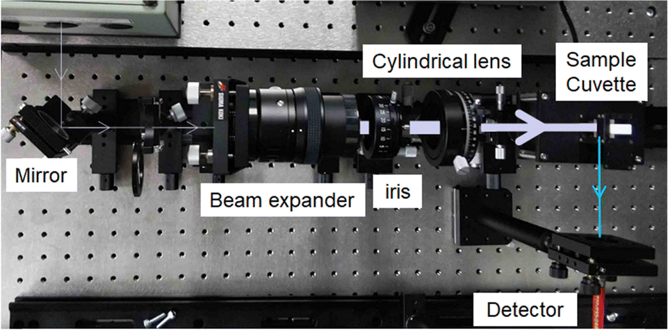 | ||
| Fig. 2 Optical pumping apparatus for the characterization of ASE and laser emission. | ||
 | ||
| Fig. 3 Blue PL spectrum of the silicon nanoclusters (dotted line) and the corresponding ASE spectrum (solid line). Inset shows the integrated PL intensity vs pumping density. | ||
Surface trap states (e.g., shallow, midgap and deep energy levels) influence the optical and electric properties in silicon nanoparticles.20,21 The existence of oxygen on the silicon surface results in oxidation to form an amorphous silica layer. Formation of the interface between silicon nanoclusters and the surface oxide gives rise to the blue fluorescence originating from the radiative recombination between electrons and holes through the silica-related emission centers.10,22 According to the analysis of time-resolved transient absorption spectral dynamics, the initially photogenerated carriers are trapped by the silica-related subband energy level within the first ∼2 ps after excitation, and transit to the localized states within ∼6 ps.21 Further study is needed but the population inversion and the buildup of optical gain might be generated between the localized state energy level and ground state in a simple three-level system upon the nanoclusters being optically pumped with a nanosecond laser.
In summary, this paper reports the blue-emitting silicon nanoclusters as a new family worthy of inclusion in the library of silicon-based laser media. In the past, the lasing in the blue-spectral range has been achieved by amplification of the defect-derived blue-light emission from the protective SiO2 layer constructed in the optical cavity, but we constructed a multi-energy level system within a nanocluster to facilitate the formation of population inversions under optical pumping conditions. This finding may pave the way for the development of silicon lasers that satisfy the required conditions for the CMOS-compatible monolithic light source.
T. T. and N. S. designed the research; H. Y., T. N. and N. S. performed the synthesis and characterization of the silicon nanoclusters; T. T. and N. S. prepared the setup for optical pumping and ASE evaluation; H.Y., T. T., T. N. and N. S. discussed the results, and H. Y. and N. S. wrote the paper.
This work was supported by the WPI program, JSPS KAKENHI (grant no. 24K01462, 24K01278 and 24K21720), Hosokawa powder technology foundation (HPTF24111), and ARIM of MEXT (JPMXP1224NM5178). H. Y. thanks the Research Fellow of JSPS and JSPS KAKENHI Grant-in-Aid (grant no. 23KJ2166).
Data availability
The data that support the findings of this study are available from the corresponding author upon reasonable request.Conflicts of interest
There are no conflicts to declare.Notes and references
- (a) D. Hahm, V. Pinchetti, C. Livache, N. Ahn, J. Noh, X. Li, J. Du, K. Wu and V. I. Klimov, Nat. Mater., 2025, 24, 48 CrossRef CAS PubMed; (b) P. Kambhampati, Nat. Nanotechnol., 2025, 20, 189 CrossRef CAS PubMed; (c) X. Lin, Y. Yang, X. Li, Y. Lv, Z. Wang, J. Du, X. Luo, D. Zhou, C. Xiao and K. Wu, Nat. Nanotechnol., 2024, 20, 229 CrossRef PubMed; (d) L. N. Quan, B. P. Rand, R. H. Friend, S. G. Mhaisalkar, T. Lee and E. H. Sargent, Chem. Rev., 2019, 119, 7444 CrossRef CAS PubMed; (e) H. Dong, C. Zhang, X. Liu, J. Yaoab and Y. S. Zhao, Chem. Soc. Rev., 2020, 49, 951 RSC.
- (a) N. Ahn, C. Livache, V. Pinchetti and V. I. Klimov, Chem. Rev., 2023, 123, 8251 CrossRef CAS PubMed; (b) N. Taghipour, M. Dalmases, G. L. Whitworth, M. Dosil, A. Othonos, S. Christodoulou, S. M. Liga and G. Konstantatos, Adv. Mater., 2023, 35, 2207678 CrossRef CAS PubMed; (c) Y. S. Park, J. Roh, B. T. Diroll, R. D. Schaller and V. I. Klimov, Nat. Rev. Mater., 2021, 6, 382 Search PubMed; (d) B. K. Barman, D. Hernández-Pinilla, O. Cretu, R. Ohta, K. Okano, T. Shiroya, J. Sasai, K. Kimoto and T. Nagao, ACS Sustainable Chem. Eng., 2023, 11, 12291–12303 CrossRef CAS.
- Y. Chan, J. S. Steckel, P. T. Snee, J. Caruge, J. M. Hodgkiss, D. G. Nocera and M. G. Bawendi, Appl. Phys. Lett., 2005, 86, 073102 Search PubMed.
- S. A. Ivanov, J. Nanda, A. Piryatinski, M. Achermann, L. P. Balet, I. V. Bezel, P. O. Anikeeva, S. Tretiak and V. I. Klimov, J. Phys. Chem. B, 2004, 108, 10625 CrossRef CAS.
- (a) C. She, I. Fedin, D. S. Dolzhnikov, P. D. Dahlberg, G. S. Engel, R. D. Schaller and D. V. Talapin, ACS Nano., 2015, 9, 9475 CrossRef CAS PubMed; (b) Y. Liao, G. Xing, N. Mishra, T. C. Sum and Y. Chan, Adv. Mater., 2012, 24, OP159 Search PubMed.
- M. L. De Giorgi, A. Perulli, N. Yantara, P. P. Boix and M. Anni, J. Phys. Chem. C, 2017, 121, 14772–14778 Search PubMed.
- Y. Wang, X. Li, J. Song, L. Xiao, H. Zeng and H. Sun, Adv. Mater., 2015, 27, 7101–7108 CrossRef CAS PubMed.
- C. S. Yang, R. A. Bley, S. M. Kauzlarich., H. W. Lee and G. R. Delgado, J. Am. Chem. Soc., 1999, 121, 5191–5195 CrossRef CAS.
- L. Canham, Faraday Discuss., 2020, 222, 10–81 RSC.
- N. Shirahata, D. Hirakawa and Y. Sakka, Green Chem., 2010, 12, 2139–2141 RSC.
- (a) K. Dohnalová, A. N. Poddubny, A. A. Prokofiev, W. D. de Boer, C. P. Umesh, J. M. J. Paulusse, H. Zuilhof and T. Gregorkiewicz, Light: Sci. Appl., 2013, 2, e47 CrossRef; (b) A. Shiohara, S. Hanada, S. Prabakar, K. Fujioka, T. H. Lim, K. Yamamoto, P. T. Northcote and R. D. Tilley, J. Am. Chem. Soc., 2010, 132, 248–253 CrossRef CAS PubMed; (c) T. M. Atkins, A. Thibert, D. S. Larsen, S. Dey, N. D. Browning and S. M. Kauzlarich, J. Am. Chem. Soc., 2011, 133, 20664–20667 CrossRef CAS PubMed.
- N. Shirahata, M. R. Linford, S. Furumi, L. Pei, Y. Sakka, R. J. Gates and M. C. Asplund, Chem. Commun., 2009, 4684 RSC.
- M. G. Panthani, C. M. Hessel, D. Reid, G. Casillas, M. Jose-Yacaman and B. A. Korgel, J. Phys. Chem. C, 2012, 116, 22463–22468 CrossRef CAS.
- B. Ghosh, T. Hamaoka, Y. Nemoto, M. Takeguchi and N. Shirahata, J. Phys. Chem. C, 2018, 122, 6422–6430 CrossRef CAS.
- (a) M. Dasog, G. B. De Los Reyes, L. V. Titova, F. A. Hegmann and J. G. C. Veinot, ACS Nano, 2014, 8, 9636 CrossRef CAS PubMed; (b) R. M. Sankaran, D. Holunga, R. C. Flagan and K. P. Giapis, Nano Lett., 2005, 5, 537–541 CrossRef CAS PubMed.
- D. Amans, S. Callard, A. Gagnaire, J. Joseph, F. Huisken and G. Ledoux, J. Appl. Phys., 2004, 95, 5010–5013 CrossRef CAS.
- I. T. Cheong, W. Morrish, W. Sheard, H. Yu, B. T. Luppi, L. Milburn, A. Meldrum and J. G. C. Veinot, ACS Appl. Mater. Interfaces, 2021, 13, 27149–27158 CrossRef CAS PubMed.
- Y. Qian, Q. Wei, G. D. Pozo, M. M. Mróz, L. Lüer, S. Casado, J. Cabanillas-Gonzalez, Q. Zhang, L. Xie, R. Xia and W. Huang, Adv. Mater., 2014, 26, 2937 CrossRef CAS PubMed.
- J. Lin, G. Zhu, B. Liu, M. Yu, X. Wang, L. Wang, W. Zhu, L. Xie, C. Xu, J. Wang, P. N. Stavrinou, D. D. C. Bradley and W. Huang, ACS Macro Lett., 2016, 5, 967–971 CrossRef CAS PubMed.
- B. Ghosh, H. Yamada, K. Nemoto, W. Jevasuwan, N. Fukata, H. T. Sun and N. Shirahata, Small Sci., 2024, 4, 2400367 CrossRef CAS PubMed.
- P. A. Piatkowski, N. A. Abbasi, W. M. Awad, P. Naumov and A. S. Alnaser, J. Phys. Chem. C, 2024, 128, 18338–18350 CrossRef CAS.
- D. Tan, Z. Ma, B. Xu, Y. Dai, G. Ma, M. He, Z. Jin and J. Qiu, Phys. Chem. Chem. Phys., 2011, 13, 20255–20261 RSC.
Footnote |
| † Electronic supplementary information (ESI) available. See DOI: https://doi.org/10.1039/d5cc01428j |
| This journal is © The Royal Society of Chemistry 2025 |