
Emulation of neuron and synaptic functions in spin–orbit torque domain wall devices†
Durgesh
Kumar
a,
Ramu
Maddu
a,
Hong Jing
Chung
b,
Hasibur
Rahaman
a,
Tianli
Jin
a,
Sabpreet
Bhatti
a,
Sze
Ter Lim
 b,
Rachid
Sbiaa
c and
S. N.
Piramanayagam
*a
b,
Rachid
Sbiaa
c and
S. N.
Piramanayagam
*a
aSchool of Physical and Mathematical Sciences, Nanyang Technological University, 21 Nanyang Link, Singapore, 637371, Singapore. E-mail: prem@ntu.edu.sg
bInstitute of Materials Research and Engineering, A*STAR, 2 Fusionopolis Way, Innovis, 138634, Singapore
cDepartment of Physics, College of Science, Sultan Qaboos University, P.O. Box 36, PC 123, Muscat, Oman
First published on 6th August 2024
Abstract
Neuromorphic computing (NC) architecture has shown its suitability for energy-efficient computation. Amongst several systems, spin–orbit torque (SOT) based domain wall (DW) devices are one of the most energy-efficient contenders for NC. To realize spin-based NC architecture, the computing elements such as synthetic neurons and synapses need to be developed. However, there are very few experimental investigations on DW neurons and synapses. The present study demonstrates the energy-efficient operations of neurons and synapses by using novel reading and writing strategies. We have used a W/CoFeB-based energy-efficient SOT mechanism to drive the DWs at low current densities. We have used the concept of meander devices for achieving synaptic functions. By doing this, we have achieved 9 different resistive states in experiments. We have experimentally demonstrated the functional spike and step neurons. Additionally, we have engineered the anomalous Hall bars by incorporating several pairs, in comparison to conventional Hall crosses, to increase the sensitivity as well as signal-to-noise ratio (SNR). We have performed micromagnetic simulations and transport measurements to demonstrate the above-mentioned functionalities.
New conceptsIn this paper, we have introduced a novel method of sensing the domain wall position in domain wall devices. For domain wall device-based neuromorphic computing, we require the output from the synapses and neurons in terms of electrical resistance. Moreover, we should be able to read the information from all over the devices. The conventional technique based on the anomalous Hall effect has limitations as it can only sense the domain wall motion from the vicinity of the Hall bars. Therefore, it cannot be used in practical devices. In our paper, we have introduced an innovative reading mechanism that can sense the non-local magnetization change/domain wall motion from all over the device. Moreover, our results indicate that our reading scheme is (a) more sensitive to small changes to non-local magnetization and (b) improves the signal-to-noise ratio (SNR) of the output voltage. These attributions are particularly crucial when the device sizes shrink to nanometer scales. To study the efficiency of our reading scheme, we have demonstrated the functional synaptic and neuron (spike and step) devices. We believe that our innovative proposal is important from both the fundamental and practical application point of view. |
Introduction
Artificial intelligence (AI) finds growing interest in day-to-day consumer devices such as smartphones, tablets, laptops, televisions, self-driving cars, and many more.1 AI potentially performs popular cognitive tasks like image/fingerprint recognition, big-data analysis, and unmanned vehicle control in the above-mentioned consumer devices.1 Currently, these intelligent functions are being performed on conventional computing architectures, based on the von Neumann formalism, by using machine learning algorithms. In von Neumann's architecture, a huge amount of data travels back and forth between the central processing unit (CPU) and the memory unit.2 This limits the speed of the computing system, which is known as the “von Neumann bottleneck”. The speed problem inflames further due to the difference in the operating speeds of the faster CPU and the relatively slower memory unit, called the “memory wall”. Above all, the present computing system is energy inefficient. For instance, a huge amount of power (∼of the order of MW) is required to simulate the activities of a cat's brain in the present computing architecture. In contrast, the human brain requires only a few watts of power to compute the same problem. Therefore, the research community is looking for alternative computing architectures that can mimic the human brain at a low energy cost.Neuromorphic computing (NC), also known as brain-inspired computing, is one such computing architecture.2 The brain comprises billions of neurons, which are interconnected through trillions of synapses. Here, neurons act as processing units, which receive the weighted sum of multiple inputs from pre-synaptic neurons and generate an output. The synapse, however, acts as a memory unit. The synapses also form the bridge between pre-synaptic neurons and post-synaptic neurons and control the weightage of information flowing between them.
At present, several non-volatile memories are being investigated to realize NC. These include resistive random access memory (RRAM), phase change RAM (PCRAM), and ferroelectric material-based RAM (FeRAM).3–6 The fully connected neural networks utilizing the above-mentioned non-volatile memory technologies offer more efficiency in terms of operational energy and areal density as compared to complementary metal oxide semiconductor (CMOS)-based neural networks.7,8 Besides these candidates, the memory technologies using spintronic devices have also shown the potential to be used as synthetic neurons and synapses. In addition to exhibiting the advantages of RRAM, PCRAM, and FeRAM, spintronic devices promise even lower energy consumption. The energy efficiency can further be enriched by utilizing the spin–orbit torque (SOT) to operate the spintronic devices. For a deeper understanding, we compare the key features of neural networks based on the above-mentioned non-volatile memory technologies (Table 1).
| Figure of merit | Resistive | Phase change | Ferroelectric | STT-MRAM | SOT-DW devices | SOT-skyrmion devices |
|---|---|---|---|---|---|---|
| Operational energy | Low | High | High | Low | Low | Low |
| Retention | High | High | High | High | High | High |
| Endurance | Medium | Medium | Low | High | Very high | Very high |
| Feature size | Small | Small | Large | Small | Medium | Medium |
| Speed | Low | High | High | Medium | Fast | Fast |
| Signal swing | Medium | High | Medium | Medium | Medium | Low |
As can be seen in Table 1, spintronic devices may be one of the favorable choices for future NC applications. On another note, the RRAM-based NC is also being investigated with high expectations. However, the spintronic devices offer better endurance (a critical factor that decides the lifetime of a device) as compared to the resistive switching-based devices. Moreover, with the usage of SOT, an even better endurance (ideally infinite) is expected for the spintronic devices. This is because SOT-based devices are three-terminal devices and the writing current does not flow through the tunneling barrier. The resistive switching devices on the other hand are two-terminal devices and therefore offer a much weaker endurance. Other challenges associated with resistive switching devices are repeatability and reliability of the output voltage and low resistance difference between the states. The spintronic devices, however, offer much better performance concerning the above.15–18 Nevertheless, both technologies offer great potential for NC and ample research is underway by respective communities.
In spintronics, the most attractive non-volatile memory devices (in the context of the present study) for NC are based on domain walls (DWs) and skyrmions.9–14,19,20 These devices are advantageous for specific applications such as pattern recognition, machine learning, and edge computing.21 Both these devices intend to utilize magnetic tunnel junctions (MTJs). Therefore, the advantages, as discussed above, of spintronic memristors are relevant for DW as well as skyrmion-based devices. However, the operational controllability is better in the case of DW devices as compared to skyrmion devices.22,23 More importantly, skyrmions give rise to a much smaller output signal compared to the DW devices. In conclusion, the DW devices are relatively more mature and are easier to implement in the existing technology.
For the DW devices to be utilized as synapses and neurons, it is important to understand the basic operational prerequisites. The synaptic functions require multiple resistance states in DW devices to offer the weighted sum of signals (from various pre-neurons) to post-neurons. This can be achieved by controllably pinning the DWs at multiple desired positions, called the artificial pinning sites. The pinning sites are created by locally changing the magnetic properties (named magnetic or non-geometrical pinning sites) or geometry (named geometrical pinning sites) of the devices. In the past, a few concepts of magnetic as well as geometrical pinning sites have been proposed to realize artificial pinning sites. Here, we briefly describe a few major concepts. Polencuic et al. utilized the exchange bias and demonstrated the DW pinning.24 Subsequently, Jin et al. studied the concepts of local non-magnetic metal diffusion,25 implantation of non-magnetic ions,26 and localized exchange coupling23,27 and demonstrated the pinning of the DWs. More recently, Kumar et al. fabricated the pinning sites by altering the interfacial Dzyaloshinskii–Moriya interaction (iDMI) locally and showed multi-resistance states using micromagnetic simulations.28 Although the above studies revealed some important physical and technological concepts, the fabrication of non-geometrical pinning sites involves complicated lithography steps. Therefore, they are not industry-friendly options.22
In the category of geometrical pinning sites, a few important designs have also been studied. For example, Parkin et al. studied the DW devices with triangular notches and demonstrated the successive DW pinning at the pinning sites.29 Similarly, Liu et al. achieved synaptic functions in the DW devices with double-sided notches.30 The fabrication of notches does not fit to the applications as this carries a severe scalability problem. This can be understood in the following manner. Suppose the depth of the notch is ‘F’, then the width of the DW device must be larger than ‘F’ (say ‘3F’). Therefore, if ‘F’ is the smallest width that can be achieved using a particular lithography technique, the wire width will always be larger than the resolution (3F). Later, the DW devices with steps in the thickness of the magnetic layer (and therefore, steps in perpendicular magnetic anisotropy) were also studied for DW pinning.28,31 However, the wires with stepped thickness require complicated lithography steps. Therefore, they are not application-friendly. As an alternative concept, Borders et al. fabricated Hall bar devices from the (Co/Ni)n ferromagnetic (FM) wire and demonstrated multiple resistance states.32 The Laplace pressure on the DW at the Hall bar junction generates effective pinning. Later, Cai et al. fabricated a DW device (from a full MTJ stack) with increasing width of the wire and demonstrated the multiple-resistance states.33 Similar to the previous case, the Laplace pressure on the DWs was utilized to pin the DWs. The Laplace pressure in such designs may not be able to generate strong pinning on the DWs; therefore, deeper research may be needed to improve the suitability of the above two methods for applications. Siddiqui et al. demonstrated the multi-resistance states in the MTJ device with a discrete reference layer.8 Despite the study of several important designs, there is still a need to research a more efficient method to pin the DWs.
On the other hand, neurons receive inputs from several other neurons and once the strength of the input(s) exceeds a threshold value, an output is generated. In addition, the neurons need to be reset just after generating an output. Hasan et al. performed simulations and studied a neuron device where a stray field from a neighboring FM wire caused the leaking or self-reset.34 Later, Mah et al. proposed and simulated a neuron device with a graded anisotropy field (Hk = 2Ku/Ms).35 Sato et al. recorded GHz oscillations of the DWs in the z-shaped DW devices for fabricating artificial neurons.36 Moreover, Kumar et al. performed micromagnetic simulations in an FM wire with local iDMI and observed that the DW oscillates at GHz frequency.37 A few other researchers studied the oscillations of the DWs in the DW devices for fabricating synthetic neurons.7,38 The majority of the research on DW device-based neurons utilizes simulation and experimental work is only at the primitive stage.
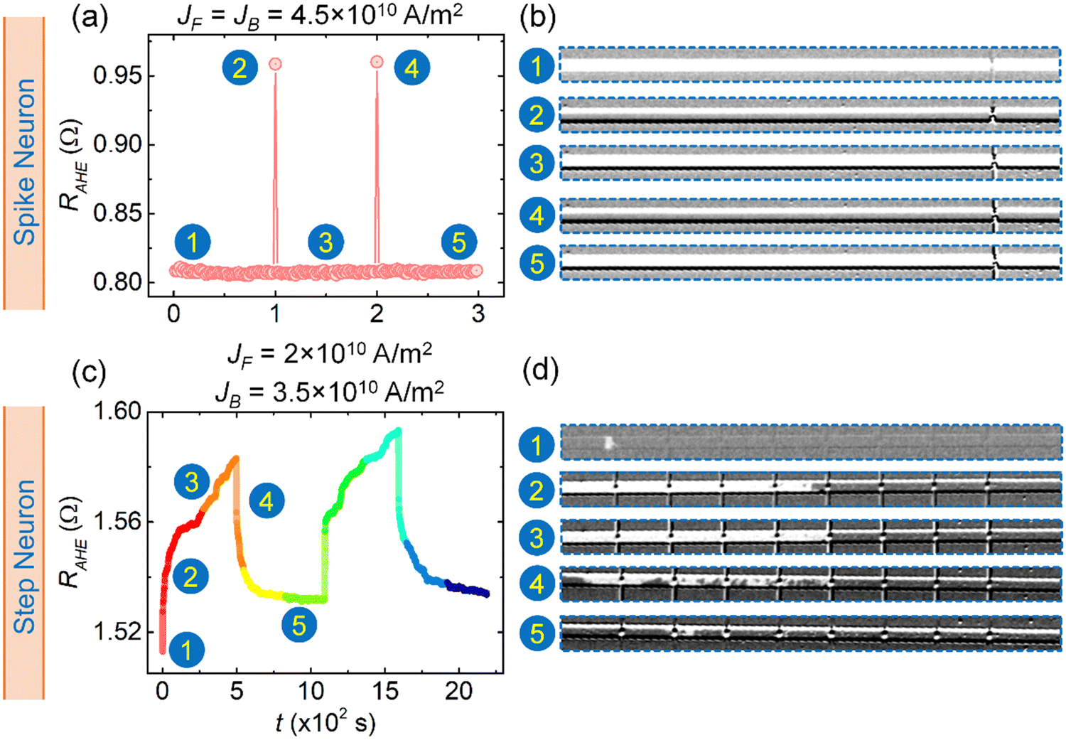
Therefore, there is a need to study more efficient synaptic and neuron devices for their potential applications in NC. With the above theme in mind, our paper aims to (a) demonstrate the functional synaptic devices wherein the synaptic weights (multiple resistance states) are represented by the position of DWs as measured by anomalous Hall voltage and (b) demonstrate integration (motion of DWs) and fire mechanisms of neurons in the absence of magnetic tunnel junctions (MTJs). For this, we have performed detailed transport experiments as well as micromagnetic simulations. For synaptic applications, we have proposed the idea of meander devices, where two segments of the DW devices adjoin at an offset of “d” (Fig. 1(a)). The junction of the neighboring DW device segments functions as an artificial pinning site. When the DW reaches and is about to leave the pinning site, it experiences a geometrical opening. Therefore, the DW experiences a torque due to Laplace pressure on the DW. This torque tries to bring the DW towards the center of the pinning site. Simultaneously, the SOT tries to move the DW in the forward direction. In the balanced situation of the two torques, the DW pins at the pinning site. Moreover, the DW can only be depinned from the pinning site when a higher current density is applied. More importantly, unlike the Hall bar design, the Laplace pressure on the DW is controllable in the meander design. This can be done by altering the offset between the DW device segments. Therefore, our design offers more controlling knobs from the application point of view. In contrast, we studied the DW motion in straight DW devices for neuron devices. We utilized SOT from the W layer to drive the DWs in our devices and demonstrated the DW motion at relatively low current densities. Moreover, we measured the anomalous Hall voltage to read the instantaneous DW position. For the case of spike neurons, we fabricated conventional Hall bar electrodes at the right end of the device. Once the DW reaches the vicinity of the read probe, a spike in the output voltage occurs. However, for the synaptic devices and step neurons, we employed a novel reading strategy. Here, we fabricated multiple pairs of equally spaced Hall probes throughout the devices. This enabled us to achieve (a) the nonlocal output signal, (b) increased signal-to-noise ratio, and (c) improved sensitivity. The details of our simulation and experimental results will be discussed in the relevant sections of the paper.
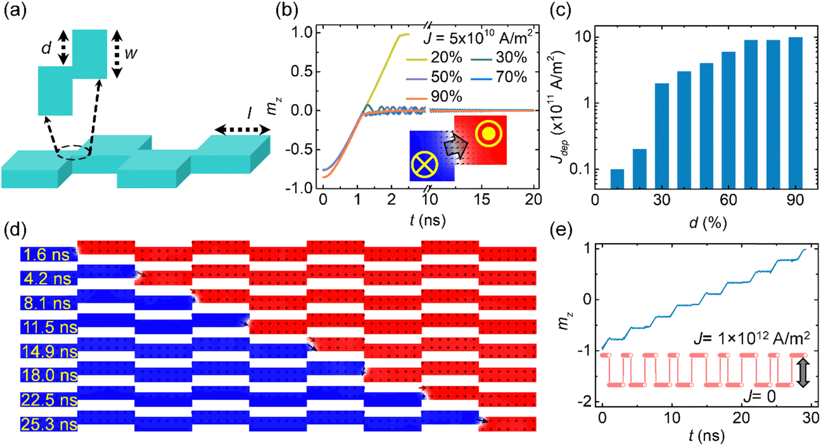 | ||
| Fig. 1 (a) Schematic diagram of the meander-shaped synaptic devices. Here, the domain wall (DW) device segments (with the length and width of l and w, respectively) connect at an offset of “d”. (b) The plot of “mz” vs. “t” for a meander device with one pinning site. These simulations were performed for different offset values ranging from 10 to 90% in steps of 10%. All these simulations were performed at J = 5 × 10¹⁰ A m−2. The figure in the inset shows the stable magnetization state when the DW is pinned at the pinning site. (c) The graph of Jdep as a function of offset “d”. (d) The instantaneous magnetization state at different simulation times to demonstrate the DW pinning at successive pinning sites. (e) The “mz” vs. “t” graph, which illustrates the intermediate magnetization states. The inset is the corresponding current density profile. | ||
Results and discussion
Domain wall-based synaptic devices
In all the simulations, we first inserted a ↓→↑ type DW, which is supported by the given iDMI constant of the material system.41 Subsequently, we applied the electrical current (DC/pulsed current) to push the DW from one end of the device to the other. The magnitude of the current density (J) was varied from 1 × 10¹⁰ A m−2 to 1 × 10¹² A m−2. The z-component of the magnetization (mz) was utilized to represent the DW position in our simulations.
First, we simulated the DW motion in meander-shaped DW devices with one pinning site (two meander segments). As mentioned earlier, we varied “d” from 10% to 90% (in steps of 10%) in simulations to get a deeper insight. As shown in Fig. 1(b), when a J of 5 × 10¹⁰ A m−2 is applied, the DW moves from the left end of the wire and gets pinned at the pinning site for “d” of 30% and higher. The DW does not pin for the offset values of 10% and 20%. The inset of Fig. 1(b) shows the stable magnetization state after the DW gets pinned for the case of d = 40% and J = 5 × 10¹⁰ A m−2. A similar stable magnetization state was observed in all the other pinning events.
Subsequently, we performed these simulations for the full range of current densities. For an offset of 10%, the DW does not pin at any of the studied current densities. However, the DW pinning was observed only for J = 1 × 10¹⁰ A m−2 in the meander devices with d = 20%. For higher offset values, the DW pinning was observed for a large range of current densities. Notably, no domain wall depinning was observed for d = 90%. Please refer to Section S1 (ESI†) for the corresponding phase diagram. We defined the current density beyond which the DW does not pin at the pinning site as depinning current density (Jdep).23 As shown in Fig. 1(c), the depinning current density increases with the increase in the offset. This confirms our hypothesis that the pinning strength increases as “d” increases and it becomes extremely strong at d = 90%.
Based on the results for meander devices with one pinning site, we then studied the DW motion in the wire with 8 pinning sites (9 meander segments). The aspect ratio (w![[thin space (1/6-em)]](https://www.rsc.org/images/entities/char_2009.gif) :l, Fig. 1(a)) for every meander segment was kept at 1:4, the same as in devices with one pinning site. Therefore, the total length of the devices increased to 1152 nm. All the other parameters were kept the same as in the previous simulations. The current density with a magnitude of 1 × 10¹² A m−2 was utilized in the form of pulses. Besides, the pulse width was optimized in such a way that the DW travels from one pinning site to the next in one pulse. Similar to previous simulations, we first inserted ↓→↑ DW in the left-most segment, and then a current pulse (|J| = 1 × 10¹² A m−2) was applied to push the DW to the first pinning site. Subsequently, the current was switched off for 2 ns. During this period, the DW stays at the first pinning site. Then another current pulse was applied to push the DW to the second pinning site and again the current was switched off for 2 ns. This process was continued until the DW swept the whole device. The results of this set of simulations are presented in Fig. 1(d) and (e). Here, every image illustrates the instantaneous magnetization state at a given simulation time (as indicated in yellow color). The blue and red colors represent the magnetization in −z and +z directions, respectively (inset of Fig. 1(b)). We plotted the domain wall position (mz) vs. simulation time (t) (Fig. 1(e)). We observed systematic pinning and depinning of the DW at every pinning site, resulting in ten multiple resistance states. The inset of Fig. 1(e) shows the profile of the pulsed current applied during these simulations. The DW exhibits damped oscillatory motion before it settles down at every pinning site. After understanding the detailed domain wall dynamics in simulations, we performed experiments to demonstrate the synaptic performance.
:l, Fig. 1(a)) for every meander segment was kept at 1:4, the same as in devices with one pinning site. Therefore, the total length of the devices increased to 1152 nm. All the other parameters were kept the same as in the previous simulations. The current density with a magnitude of 1 × 10¹² A m−2 was utilized in the form of pulses. Besides, the pulse width was optimized in such a way that the DW travels from one pinning site to the next in one pulse. Similar to previous simulations, we first inserted ↓→↑ DW in the left-most segment, and then a current pulse (|J| = 1 × 10¹² A m−2) was applied to push the DW to the first pinning site. Subsequently, the current was switched off for 2 ns. During this period, the DW stays at the first pinning site. Then another current pulse was applied to push the DW to the second pinning site and again the current was switched off for 2 ns. This process was continued until the DW swept the whole device. The results of this set of simulations are presented in Fig. 1(d) and (e). Here, every image illustrates the instantaneous magnetization state at a given simulation time (as indicated in yellow color). The blue and red colors represent the magnetization in −z and +z directions, respectively (inset of Fig. 1(b)). We plotted the domain wall position (mz) vs. simulation time (t) (Fig. 1(e)). We observed systematic pinning and depinning of the DW at every pinning site, resulting in ten multiple resistance states. The inset of Fig. 1(e) shows the profile of the pulsed current applied during these simulations. The DW exhibits damped oscillatory motion before it settles down at every pinning site. After understanding the detailed domain wall dynamics in simulations, we performed experiments to demonstrate the synaptic performance.
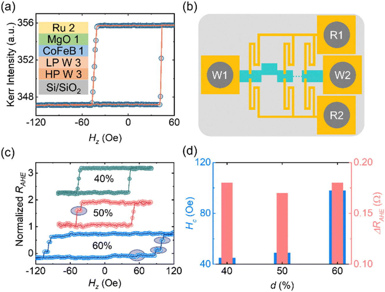 | ||
| Fig. 2 (a) The magnetic hysteresis loop of the film stack used in this study. Inset: The schematic diagram of the film stack. (b) The schematic of the synaptic devices with uniquely designed read and write electrodes. (c) The R–H loop, illustrating the multiple resistance states in our synaptic devices. (d) The plots of Hc and ΔRAHE as a function of “d” in meander devices. | ||
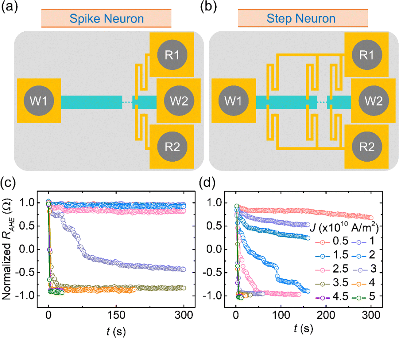
To experimentally study the DW dynamics in our synaptic and neuron devices, we fabricated micro-meter-sized meander and straight wires, respectively. The dimensions of these devices were 900 μm × 20 μm. Based on our simulation results, the offsets (d) of meander devices were chosen to be 40, 50, and 60% (with respect to the width of the DW devices). To achieve different functional outputs, we proposed a novel engineering design for fabricating the Hall bars. In the conventional Hall bar design, the output is measured using one pair of pins.43 In this case, the major portion of the output signal is collected from the regions in the vicinity of the Hall crosses. Any change in magnetization far from the Hall probes, usually a very weak signal, cannot be detected with high sensitivity. In contrast, we proposed and studied the following novel design. For the synaptic device, we need to collect the signal from all over the device. Therefore, we fabricated eight pairs of equispaced Hall bar pins. Moreover, the dimensions of Hall crosses were chosen in such a way that the maximum writing current flows through the current channel/DW devices. A similar design of Hall bars was utilized for the case of step neurons. This helps in improving the sensitivity of the output signal as well as enhancing the signal-to-noise ratio (SNR). The reading strategy for synaptic and step neuron devices is schematically presented in Fig. 2(b). For the case of spike neurons, we fabricated one pair of Hall bars (conventional design) at the right end of the device (Fig. 6(a)). Once the DW reaches the vicinity of the Hall bar, the output in the form of the spike can be obtained. We have presented more details of the device fabrication in the Methods section and Section S2 (ESI†).
Firstly, we measured the R–H loops of the synaptic devices (with offsets d: 40, 50, and 50%) (Fig. 2(c)). For this, we first saturated the devices with a large out-of-plane (OOP) magnetic field of −1000 Oe. Subsequently, we swept the OOP magnetic field from −Hz to +Hz at a sweep rate of 1 Oe s−1 (step size: 2 Oe). At every field value, we applied a reading current density with a magnitude of 5 × 10⁸ A m−2 (Iread = 100 μA) and a pulse width of 0.2 s. Corresponding to such reading pulses, we captured the magnetization state of the devices in terms of anomalous Hall voltage (VAHE). From the anomalous Hall voltage, we estimated the anomalous Hall resistance (RAHE) following Ohm's relation (RAHE = VAHE/Iread). An identical experimental process was followed while sweeping the OOP magnetic field from +Hz to −Hz. Please see the Methods section for additional details on the experimental procedure employed during the R–H measurements.
For d = 40%, we observed a sharp DW motion-mediated magnetization switching (without any intermediate magnetization state). However, once the offset increases to 50% and 60%, the intermediate magnetization states were observed. For instance, we observed a total of 3 states for d = 50% and 5 states for d = 60%. For a clearer representation of the magnetization states, we have plotted the data from 0 to ±Hz-max for all the studied devices (Section S3, ESI†). This means that the pinning strength of the pinning sites increases as “d” increases. This result is consistent with the simulation results. Interestingly, the device coercivity (Hc-device) increases as “d” increases (Fig. 2(d)). For d = 40%, Hc-device was found to be 45 Oe, which is similar to the thin film coercivity (44 Oe). However, the same increases to 98 Oe for d = 60%, which suggests that the pinning strength increases as the offset value increases. In addition to the change in coercivity, we also estimated the difference in anomalous Hall resistance between the up and down magnetization states and found similar values for all the meander devices (Fig. 2(d)). This is expected as the read probe design is identical in all the synaptic devices. Additionally, we also performed the magnetization switching experiments while sweeping the electrical current (in the presence of an in-plane (IP) magnetic field) and observed the multi-resistance states. Please see Section S5 (ESI†) for detailed discussions of the results from the current sweeping experiments. These results are also summarized in Table 2.
| d (%) | H c (Oe) | ΔRAHE (Ω) | J dep (A m−2) | Number of resistance states | ||
|---|---|---|---|---|---|---|
| H z sweep | I sweep | Pulsed current | ||||
| 40 | 45 | 0.18 | 2.5 × 10¹⁰ | 2 | 2 | 5 |
| 50 | 49 | 0.17 | 4 × 10¹⁰ | 3 | 5 | 7 |
| 60 | 98 | 0.18 | 5 × 10¹⁰ | 5 | 7 | 9 |
Subsequently, we performed SOT-induced DW motion experiments in our synaptic devices. After saturating the devices, we applied the current pulses of a certain magnitude. The current density (J) was varied from 5 × 10⁹ A m−2 to 5 × 10¹⁰ A m−2 in most of the cases (unless specified). A simultaneous longitudinal magnetic field of 500 Oe was applied in all cases. The directions of the current and the in-plane magnetic field were kept the same as in the current sweeping experiments and illustrated in Fig. 3(a). Further details on the experimental procedure are included in the Methods section. As one can see in Fig. 3(a), for the case of an offset of 40%, when the current pulses of J = 3 × 10¹⁰ A m−2 together with an in-plane magnetic field of 500 Oe are applied in the synaptic devices, a reversed domain gets nucleated and the DW moves from the left end to the right end of the device. The nature of the DW motion is consistent with the SOT-driven DW motion in similar systems.41 We repeated these experiments for synaptic devices with an offset of 50% and 60%. These results suggest that the pinning strength of the pinning sites increases as the magnitude of the offset increases. Again, these results are consistent with the previous results. Moreover, we also witnessed multiple resistive states as a result of uniform current pulses. These results are presented in detail in Section S6 (ESI†).
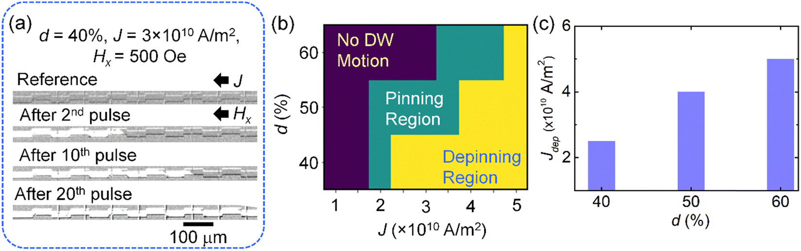 | ||
| Fig. 3 (a) The results of Kerr microscopy to demonstrate the DW dynamics in meander synaptic devices with d = 40%, J = 3 × 10¹⁰ A m−2, and Hx = 500 Oe. (b) The phase diagram of DW dynamics in meander devices as a function of “d” and “J”. (c) The graph of depinning current density (Jdep) vs. offset “d” values. | ||
To understand the DW dynamics in synaptic devices in greater detail, we plotted the phase diagram of DW dynamics as a function of offset and current density (Fig. 3(b)). We have performed the experiments for the current density range starting from 5 × 10⁹ A m−2 to 5 × 10¹⁰ A m−2. However, we have shown the results from 1 × 10¹⁰ A m−2 to 5 × 10¹⁰ A m−2 for a clear presentation of the data. The results for J = 5 × 10⁹ A m−2 are identical to those observed for J = 1 × 10¹⁰ A m−2. Here, the violet, green, and yellow colors represent the “no domain wall motion region”, “domain wall pinning region”, and “domain wall depinning region”, respectively. The pinning region is the narrowest for the offset of 40% and becomes wider as the “d” value increases. Moreover, the pinning strength of the whole DW device increases significantly for the devices with d = 60%, which is consistent with our R–H loop results. The depinning current density (Jdep) increases as the offset increases. This is also shown in Fig. 3(c) and Table 2 for better understanding. From these results, we can see that pinning is weakest for d = 40% and strongest for d = 60%.
Another interesting observation is that the required current densities 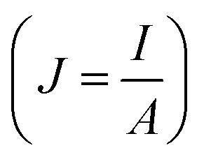 to drive the DWs in our devices are significantly lower as compared to the average current densities reported in the literature. The observation of lower current densities in SOT-driven DW motion in our devices is attributed to the following: (a) a lower depinning field (20 Oe) of our samples compared to that of typical Pt/Co samples (∼100 to ∼600 Oe);41 (b) an improved spin Hall angle of our samples (−0.14) compared to that of Pt/Co samples (∼0.08);41 and (c) the pulse width of the current pulses is 200 ms. Although we have set the time interval between the consecutive current pulses at 2 s (to minimize the Joule heating), the role of Joule heating in the domain wall motion cannot be completely neglected.
Furthermore, we performed experiments to study the multi-resistance states in meander devices (Fig. 4). The direction of the current density and in-plane magnetic field in these experiments is consistent with the previous experiments. Similarly, the pulse width and the time interval between consecutive pulses remained the same. The magnitudes of the current densities were optimized to maximize the number of resistance states in all the devices. As observed in Fig. 4(a), a total of 5 resistance states were obtained for d = 40%. This number can be increased to 7 when d was increased to 50% (Fig. 4(b)). Fig. 4(c) shows the corresponding Kerr microscopy images (in polar configuration), which illustrate the pinning of the DW at different pinning sites. Our results indicate that the fabrication-induced defects also help in pinning the domain walls. Nevertheless, the multiple resistance states in the output electrical signal are more important. Here, images ‘1’ and ‘2’ represent the reference and nucleated states, respectively. In subsequent current density pulses, the nucleated domain expands. For simplistic and more application-friendly operations, we used SOT to nucleate the reversed domains. Note that a bright (white) region at the right end of the device in image ‘4’ is a result of an SOT-induced nucleation (and expansion). This aspect will be discussed in detail in subsequent paragraphs. Since the DW stays pinned at the pinning site for a significant time, we observe the grey regions, representing the magnetization in a direction opposite to the magnetization in the white region, in the images. Moreover, when the DW sweeps the whole device due to a current density larger than the depinning current density, the grey region gets converted to the white region. The vertical dark and bright lines in Kerr images correspond to the noise (arising from the drift in Kerr microscopy) and the position of the read probes. We also observed that the instantaneous magnetization state slightly differs when it is read using Kerr microscopy and the proposed method. This is because the Hall voltage reading using the proposed method is more sensitive to the change in magnetization in the vicinity of the read probes.
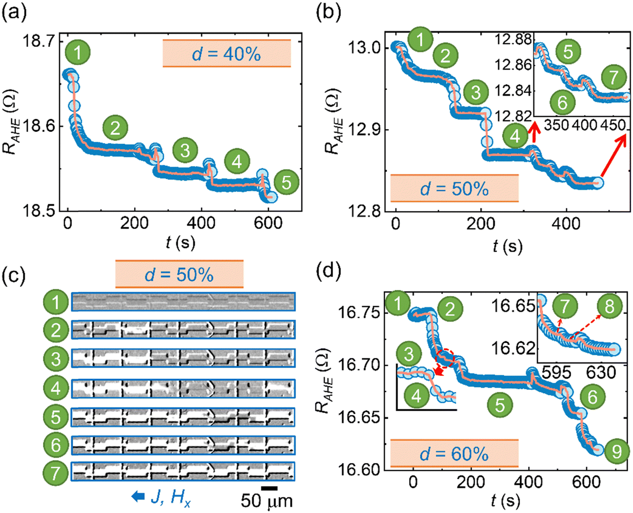 | ||
| Fig. 4 The illustration of multiple resistance states for meander devices with an offset of (a) 40%, (b) 50%, and (d) 60%. (c) Kerr microscopy images, which show the systematic pinning and depinning at different pinning sites for an offset “d” of 50% (corresponding to panel (b)). | ||
In addition, we also discuss the following after a careful inspection of Fig. 4(c). A sequential DW motion from one end of the meander device to the other is a perfectly ideal case. However, there is a possibility of the following events in the SOT-driven DW motion in DW devices with geometrical non-uniformity. (i) At the constrictions, the current density is higher as compared to the rest of the device segments. This results in higher SOT efficiency and Joule heating at the constrictions (for the same current density). Therefore, there is a possibility of the nucleation of reversed magnetic domains at the constriction regions, which in turn may disrupt the sequential DW motion. (ii) During the fabrication of the read probes, we hypothesize that there may be an introduction of process-induced defects. They may also cause the nucleation of the reversed domain during the DW motion. Therefore, it is difficult to completely neglect the possibility of nucleation of reversed domains in DW devices with local geometric amendments. Nevertheless, it is more important to achieve multiple resistance states in a repeatable and controlled manner. When d increases to 60%, the pinning becomes stronger, and the number of resistance states increases to 9. This result is presented in Fig. 4(d). The summary of the number of resistance states for all the studied meander devices is summarized in Table 2.
As can also be seen in Fig. 4, the resistance change exhibits some non-uniformity when the magnetization states change. The non-uniformity due to the intrinsic and external edge defects arising due to the device fabrication process is unavoidable in spintronic devices. On another note, the reading current is non-linear in domain wall magnetic tunnel junctions (MTJs). This means that even if we integrate these devices in a full MTJ stack, there is a possibility of an unequal jump between consecutive resistance states. As stated earlier, this will be a problem with all the spintronic devices spanning in the lateral direction. Now let us try to understand the sources of non-linearity in the readout signal when Hall bars are used. Conventionally, we fabricate one pair of Hall bars to sense the change in the transverse voltage (anomalous Hall voltage). This change in voltage is proportional to the change in the magnetization state of the device. However, the change in transverse voltage is more sensitive to the change in magnetization state in the vicinity of the Hall bars. The sensitivity of the signal may be small or negligible for any change in magnetic state far from the Hall bar position.
To overcome this issue and read the non-local change in magnetization, we proposed the idea of multiple pairs of Hall bars. In addition to non-local sensitivity, the proposed scheme also helps to increase the signal-to-noise ratio. Although we placed the Hall bars at equal spacings, the resultant signal can still exhibit non-linearity. This is because the output is sensitive to the change in magnetization in the vicinity of any of the Hall probes. However, the sensitivity of the magnetic signal far from the probes (say from the middle of the two probes) may be slightly lower. Therefore, there may be non-linearity in the output signal. This problem can be minimized by increasing the number of probes and therefore minimizing the spacing between the individual Hall probes. Alternatively, the use of MTJs would resolve this issue. Nevertheless, a systematic optimization of both the reading techniques would greatly help to observe a suited read-out signal. We think our study establishes a proof-of-concept for this novel reading technique. This provides new insights not only in practical application but also in fundamental physics.
Here, we would also like to comment on the suitability of our devices in practical applications from the required writing current point of view. We have utilized the current source with the current values (in the form of pulses) in the range starting from 1 mA to 10 mA to drive the DWs. Moreover, the pulse widths were fixed at 0.2 s in all the experiments. To minimize the effect of the Joule heating, we fixed the time interval between the consecutive current pulses at 2 s. We could not reduce the pulse widths to smaller values than the above-mentioned value due to the limitations in our measurement system. The longitudinal resistances were observed at ∼5–6 kΩ in all our studied devices. Therefore, following Ohm's relation, the voltage values range from 5 to 50 V. Therefore, the devices with micro-meter dimensions are difficult to implement in fully connected neural networks. For practical applications, the width of the devices must be reduced to at least 100 nm or less. At such dimensions, the required current and voltage values will be far less for similar current densities.
Another important observation is that when magnetization changes between two consecutive states, we often observe a peak. This is because of the following reasons. The flat portions in RAHEvs. t graphs represent the pinning of the DWs. To depin the DW from the pinning site, a higher current density is required. Once the DW is depinned from the pinning site and reaches the DW device segment, we again apply a smaller current density for DW motion. A higher current density to depin the DWs would also cause a higher Joule heating and therefore slightly larger RAHE.44 This, we think is the reason for a peak in resistance when the DW makes a transition from one resistance state to another.
Domain wall-based neurons
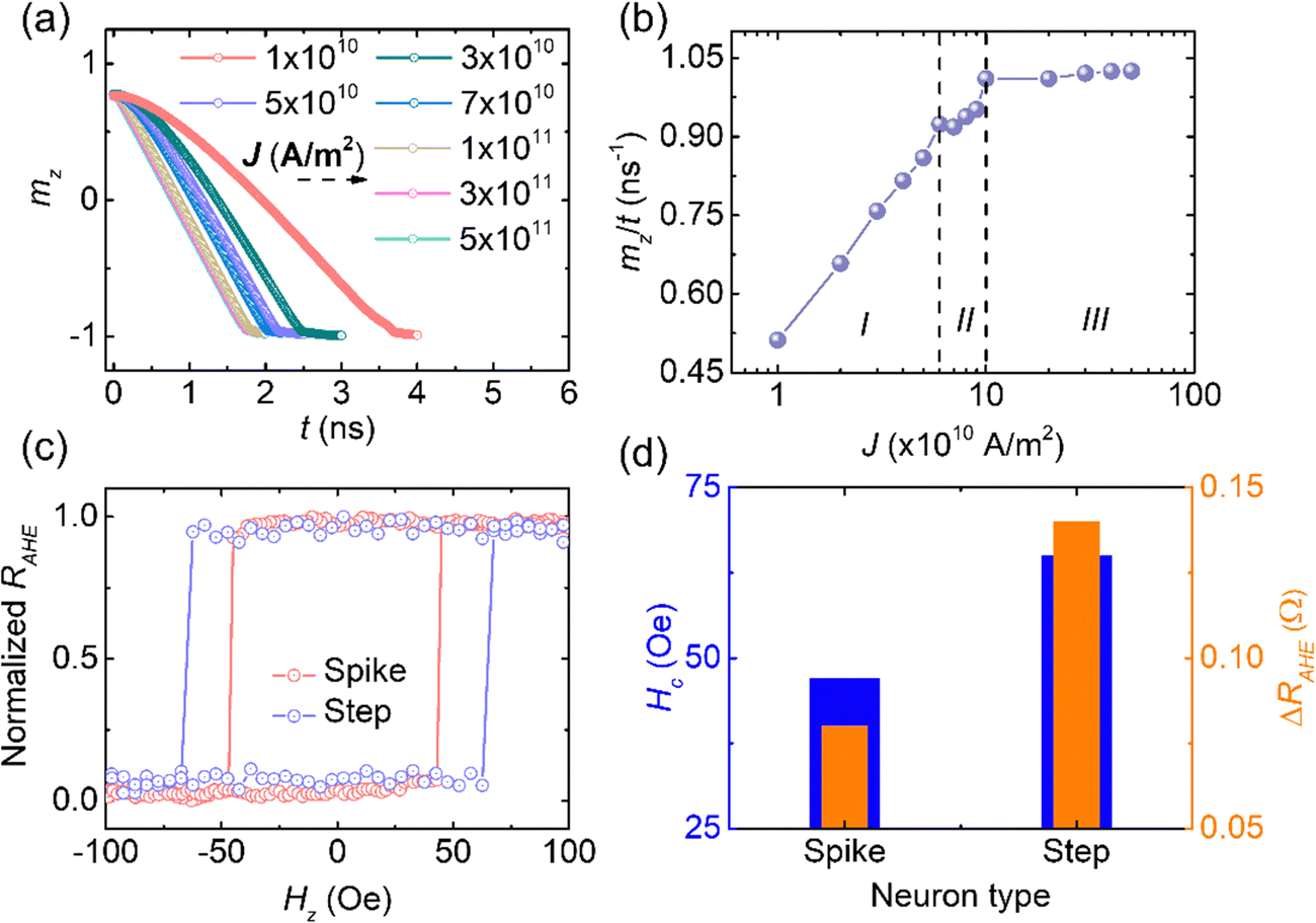 | ||
| Fig. 5 Simulation results: (a) the demonstration of domain wall (DW) motion in a straight (neuron) device for different current density values. (b) The plot of mz/t (∝ DW velocity) vs. J for neuron devices. Experimental results: (c) the graph of RAHEvs. OOP magnetic field for both types of neuron devices. (d) The comparison of coercivity and ΔRAHE for two different types of neuron devices. | ||
As one can see in Fig. 5(a), the slope of the mzvs. t graph increases as J increases. This means that the DW velocity increases with J (region I, Fig. 5(a)). Here, mz/t is proportional to the DW velocity. However, beyond J = 1 × 10¹¹ A m−2, the slope becomes constant. This suggests that a maximum in SOT efficiency (for given magnetic parameters) occurs at 1 × 10¹¹ A m−2 and it does not increase further (region III, Fig. 5(b)). We have also observed a drop in domain wall velocity at J = 7 × 10¹⁰ A m−2. This is because of the Walker breakdown during the DW motion in the perfect nanowire (region II, Fig. 5(b)).45–48 Please refer to Section S7 (ESI†) for a detailed discussion of these three regions of DW motion.
| Neuron type | H c (Oe) | ΔRAHE (Ω) | Nature of domain wall motion | ||
|---|---|---|---|---|---|
| No DW motion (region I) | Slow DW motion (region II) | Fast DW motion (region III) | |||
| Spike | 47 | 0.08 | 5 × 10⁹–2.5 × 10¹⁰ A m−2 | 3 × 10¹⁰ A m−2 | 3.5 × 10¹⁰ A m−2 and above |
| Step | 65 | 0.14 | — | 5 × 10⁹–3 × 10¹⁰ A m−2 | 3.5 × 10¹⁰ A m−2 and above |
 | ||
| Fig. 6 The schematic presentation of the (a) spike and (b) step neuron devices. SOT-driven DW motion for (c) spike and (d) step neuron devices for the current densities ranging from 5 × 10⁹ A m−2 to 5 × 10¹⁰ A m−2. An in-plane magnetic field of 500 Oe was applied in all cases. | ||
Another interesting observation is that the difference in anomalous Hall resistance corresponding to up and down magnetization (ΔRAHE) has doubled for the case of the step neuron compared to the same in the spike neuron. We observed that ΔRAHE is ∼0.08 Ω for devices with one pair of Hall bars (spike neurons), whereas the same was observed to be ∼0.14 Ω (step neurons) (for meander devices, it is ∼0.17–0.18 Ω) for devices with 8 pairs of Hall bars. As mentioned earlier, the only difference between the spike and step neurons is the difference in reading strategies. Therefore, it is clear that the difference arises due to the proposed novel reading strategy. This also means that in addition to providing the non-local signal from the entire device and better SNR, our novel proposal also helps in increasing the sensitivity of the output signal. This is in line with our initial hypothesis. This aspect is also important as this may help in increasing the distinguishable multiple resistance states for the synaptic devices. The anomalous Hall voltage can be defined using the following relation:49
 | (1) |
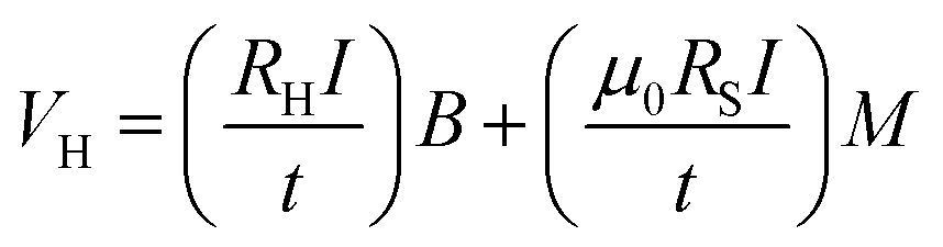 | (2) |
Subsequently, we studied the SOT-driven DW motion in our neuron devices. The experimental procedure is the same as the one described for the synaptic device. The results of this set of experiments are presented in Fig. 6(c) and (d) and Table 3. As one can see for spike neurons, the DW does not move (or negligible domain wall movement) for the current densities less than 2.5 × 10¹⁰ A m−2. This can be defined as region I of DW motion (Table 3). However, for a current density of 3.5 × 10¹⁰ A m−2 and above, the DW covers the whole DW devices in only a few current pulses (region III, in Table 3). The intermediate DW motion (region II) only occurs for a current density of 3 × 10¹⁰ A m−2. However, in the case of step neurons, the region I of DW motion disappears. The slow and controlled DW motion region (region II), where several current pulses are required to move the DWs from one end to the other, expands from J = 5 × 10⁹ A m−2 to 3 × 10¹⁰ A m−2. Similar to the case of spike neurons, for the current densities of 3.5 × 10¹⁰ A m−2 and above, fast domain wall motion was observed for the step neuron devices as well. The reason for the above difference is the process-induced defects (as described above). When the electrical current pulses are applied, the nucleation of the reversed domains is easier for the step neurons. Once a DW is inserted in the DW devices, it can be moved in subsequent current pulses. However, for the spike neurons, the insertion of the DWs is harder due to fewer nucleation sites. We have also noticed that our HP3P3 thin film samples offer low pinning site density in the as-deposited state.41 Thus, the pinning site density in spike neurons is closer to the simulated case as compared to step neurons. Nevertheless, the DWs can be moved from one end of the device to the other (for certain current densities and experimental time) for both neurons without any significant pinning. The virtue of different DW motion because of process-induced defects also helps in achieving the distinguishable spike and step neuron functions. To check the repeatability of the results, we repeated these measurements on a few more devices and observed similar results. Please see Section S9 (ESI†) for the details of these results.
We then adjusted the applied current density or in-plane magnetic field or both to achieve the spiking and step neuron behavior in the RAHE signal. For spike neuron devices, we first applied current pulses with a magnitude of 4.5 × 10¹⁰ A m−2 in the presence of an in-plane magnetic field (500 Oe). This results in the nucleation and expansion of a reversed domain. A magnetization state where all the spins point in the +z-axis was considered as the initial state (state 1 in Fig. 7(a) and (b)). When we reverse the direction of the current, the magnetization direction changes. Since the read probe is only at the right end of the wire, a change in the magnetization occurs when the domain wall reaches the vicinity of the read probe (state 2 in Fig. 7(a) and (b)). At this point, the direction of the current is reversed (same as state 1) to retain the initial magnetization state (state 3 in Fig. 7(a) and (b)). We repeated this process to demonstrate two spikes in our experiments. The magnetization states 4 and 5 are identical to states 2 and 3 (or 1), respectively. We have also studied the DW dynamics in these spike neuron devices at different current densities and observed spiking behavior. These results also indicate good repeatability of our results. These results are presented in Section S8 (ESI†). The magnitude and the direction of the in-plane magnetic field remained the same during all these experiments.
 | ||
| Fig. 7 SOT-driven domain wall (DW) motion for (a) and (b) spike and (c) and (d) step neuron devices. Figures (b) and (d) are Kerr microscopy images for different magnetization states (as indicated). | ||
Later, we performed the measurements for the step-neuron devices. First, we applied an electrical current density of magnitude 2 × 10¹⁰ A m−2 with a simultaneous in-plane magnetic field of 500 Oe. A reversed domain gets nucleated (state 1 in Fig. 7(c) and (d)) and expands upon the application of the subsequent current pulses. States 2 and 3 represent intermediate magnetization states before we reverse the direction of the current. After 500 s, we reverse the direction of the current (backward direction). In the backward direction, J = 3.5 × 10¹⁰ A m−2 and Hx = 300 Oe were utilized. The direction of the magnetic field remains unchanged. Here, the domain wall starts moving in the opposite direction. These are represented by states 4 and 5 of Fig. 7(c) and (d). Upon repeating the process of steps 1 through 5, identical results were obtained. The shift of the initial state resistance to slightly higher values is attributed to the Joule heating of the devices.
Outlook
Based on the experimental conditions and findings on our synaptic and neuron devices, we briefly discuss the advantages and limitations of our devices from the commercial application point of view.(i) As mentioned above, in domain wall (DW) devices with geometrical pinning sites, the geometry of the device is altered locally. As a result, the local current density will be different at the pinning sites for the same applied electrical current. In our devices, the change in geometry is introduced in terms of a constriction. Therefore, an increment in current density may be expected. Moreover, the constriction may result in a larger local resistance, and therefore, larger Joule heating. Consequently, one may observe the nucleation of reversed domains at the pinning sites. However, this should not be a roadblock in the applicability of meander devices as it is more important to observe multiple resistance states for synaptic applications. On another note, this can be avoided by fabricating the ferromagnetic layer with the meander geometry while maintaining the spin Hall layer without the meander structure. Based on the available concepts to pin the DWs at the geometrical pinning sites, the meander devices are one of the most efficient devices.
(ii) In general, the Joule heating is unavoidable and is always present during current-driven DW motion experiments. With our experimental parameters, we rely more on the DW motion induced by current density pulses of constant magnitude. However, the Joule heating can be controlled by (a) reducing the size of the devices, (b) reducing the pulse width of the current pulses, and (c) increasing the spin–orbit torque efficiency.
(iii) In our device, we also think that the fabrication of read probes introduces process-induced defects. This becomes more important for meander devices and step neurons. We observed that process-induced defects support in achieving distinguishable DW motion for step and spike neurons. In the meantime, they may result in the nucleation of reversed domains in meander DW devices. However, as discussed above, this will not be an issue for the applicability of meander devices as synaptic devices.
(iv) Conventionally, we utilize one pair of Hall bars to measure the change in anomalous Hall voltage, quantifying the change in the magnetization state. In the present study, we proposed the utilization of multiple pairs of Hall bars and demonstrated the advantages of (a) accessing the non-local change in magnetization, (b) increased signal-to-noise ratio, and (c) improved sensitivity. Our results are useful from both the basic engineering and application point of view. From the basic knowledge point of view, we can use this design to probe the physics of materials, which is not accessible with conventional design. For instance, if one needs to study a material with a weaker magnetic signal, the present design may prove to be crucial. From the direct application point of view, we understand and agree that the usage of the MTJ is more suited. However, the findings of our study may be useful while designing the DW device-based neurons and synapses. For example, we witnessed the usefulness of the process-induced defects for distinguishable DW motion in spike and step neurons. Although the decrement in pulse width in nano-meter-sized devices is critical, devices with optimized pinning site density are expected to provide more control in DW motion. Thus, our fabrication process may inspire the fabrication strategy of DW-MTJ devices, to achieve a striking difference in DW dynamics for spike and step neurons.
As a result, our study presents a proof-of-concept for the DW-based neuron and synaptic devices. For prototypical devices, we need to address the following challenges, including (a) the reduction in the size of the devices to sub-100 nm or less, (b) using ns-writing pulses, (c) field-free DW motion, (d) researching novel spin Hall (or even orbital Hall) materials with improved SOT efficiency, and (e) integrating our DW devices with MTJs for readback signals. Recently, a few reports have reported the development of DW-MTJ devices.8,50–52 However, more efficient devices need to be developed.
Conclusions
Owing to the suitability of DW devices for energy-efficient NC, we have studied DW device-based synapses and neurons through micromagnetic simulations and experiments. For synaptic operations, we proposed and studied the concept of meander DW devices. The depinning current density increases with the increase in offset. We found that an offset of ∼50% is most suitable for synaptic devices. We studied a novel read probe that helped in improving the sensitivity and enhancing the SNR. We demonstrated nine distinct resistance states in our synaptic devices. For neurons, we studied straight DW devices in the form of spike and step neurons. For the spike neurons, we fabricated one pair of reading probes at the right end of the devices. However, step neurons utilize the same reading strategy as in the meander devices. We found that the nature of the DW motion in step and spike neurons has a clear difference because of process-induced defects. This also helps in achieving the operations of step and spike functions and we successfully demonstrated the step and spike neuron functions in our devices. We believe our study contributes significantly toward the development of DW device-based NC architecture.Methods
Micromagnetic simulations
We performed micromagnetic simulations using the MuMax3 software,39,53–55 which uses the Landau–Lifshitz–Gilbert (LLG) equation to describe the DW dynamics: | (3) |
![[m with combining right harpoon above (vector)]](https://www.rsc.org/images/entities/i_char_006d_20d1.gif) is the locally reduced magnetization,
is the locally reduced magnetization,  is the effective magnetic field, α is the Gilbert damping parameter, and γ0 = μ0γ, where γ is the gyromagnetic ratio, defined as
  (g, e, and me are the Lande factor, electronic charge, and electronic mass, respectively). The effective field can be written as the sum of fields corresponding to different energies present in the system, which takes the following form in the present case:55
| Heff = Hexchange + Hanisotropy + Hdemag + HDMI | (4) |
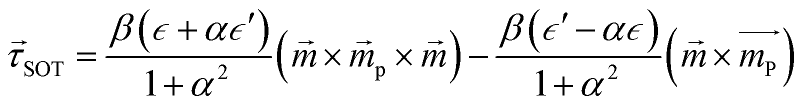 | (5) |
 | (6) |
 | (7) |
 the secondary spin torque parameter. Here, we have set the secondary spin torque parameter at zero. This means that we are only considering damping-like torque in our simulations.
First, we discuss the simulation methodology for the reference wire (neuron devices). The dimensions of the neuron devices were set at 256 nm (l) × 32 nm (w) × 1 nm (t). Here, symbols l, w, and t represent the length, width, and thickness of the device. The magnetic parameters were chosen as exchange constant (A) = 1.5 × 10⁻¹¹ J m−1, saturation magnetization = 1 × 10⁶ A m−1, anisotropy constant = 1 × 10⁶ J m−3, damping constant = 0.012, DMI constant = 0.5 mJ m−2, and spin Hall angle = −0.3. These parameters correspond to experimentally observed values in the W/CoFeB/MgO system. The cell size along the three axes was set at 1 nm × 1 nm × 1 nm, which is much smaller than the exchange length (concerning the above-mentioned parameters) lex = ∼5 nm, for our simulated system. We performed all the simulations at 0 K and for the perfect nanowire.
We first inserted the ↓→↑ type domain wall and then applied the SOT current density ranging from 1 × 10¹⁰ to 5 × 10¹¹ A m−2. Under the influence of the SOT, the DW moves from the left end of the wire to the right end without any pinning. Depending on different configurations of reading elements, which have been discussed in the paper, we can realize the step and spike neuron functionalities. We have included the videos of the DW motion for J = 1 × 10¹⁰ A m−2 and 5 × 10¹¹ A m−2 in the ESI† (Section S11) for a better understanding of the above discussion.
Further, we discuss the simulation details for meander domain wall devices with one pinning site. The dimensions of the meander devices were kept the same as that of the neuron devices. This means one segment of the meander device is 128 nm long. The offset values were varied from 10% to 90% in steps of 10%. All the geometric and magnetic parameters were kept the same as in the neuron devices except for a slightly higher spin Hall angle value of −0.37. This is because a slightly higher spin–orbit torque efficiency is required for the meander devices to depin the DWs from the pinning sites. This is particularly true for the devices with higher offset values.
Similar to the neuron case, we first inserted a ↓→↑ type DW, which is supported by the given iDMI constant of the material system in all the simulations. Subsequently, we applied the electrical current (DC) to push the DW from one end of the device to the other. The magnitude of the current density (J) was varied from 1 × 10¹⁰ A m−2 to 1 × 10¹² A m−2. The z-component of the magnetization (mz) was utilized to represent the DW position in our simulations. For a better understanding of the simulation results, we have presented the videos of DW motion in meander devices with all the studied offset values for a current density of 5 × 10¹⁰ A m−2 (Section S11, ESI†).
Lastly, we performed the simulations for meander devices with 8 pinning sites. As in the case of simulations with one pinning site, we kept the length of one segment at 128 nm. Therefore, the total length of the meander device with 8 pinning sites is 1152 nm. All the other geometrical and magnetic parameters are identical to the simulations with one pinning site. In this case, we again inserted the ↓→↑ type DW and applied the pulsed current density with the magnitude of 1 × 10¹² A m−2. The profile of the current density pulses and the simulated domain wall dynamics is presented in detail in Fig. 1. For visual understanding, we have also included the corresponding video of DW dynamics in the ESI† (Section S11). For easy access to the simulation parameters, we have summarized them in Table 4.
| S/no. | Parameter | Value |
|---|---|---|
| 1 | Device dimensions | 256 nm × 32 nm × 1 nm |
| 2 | Cell size | 1 nm × 1 nm × 1 nm |
| 3 | Exchange constant | 1.5 × 10⁻¹¹ J m−1 |
| 4 | Saturation magnetization | 1 × 10⁶ A m−1 |
| 5 | Anisotropy constant | 1 × 10⁶ J m−3 |
| 6 | Easy-axis direction | (0, 0, 1) |
| 7 | Damping constant | 0.012 |
| 8 | DMI constant | 0.5 mJ m−2 |
| 9 | Spin Hall angle | −0.3 |
| 10 | Exchange length | ∼5 nm |
| 11 | Domain wall type | ↓→↑ |
| 12 | Current density | 1 × 10¹⁰–1 × 10¹² A m−2 |
| 13 | Meander offset | 10–90% |
Thin film depositions
The film stack Si/SiO2/HP-W (3 nm)/LP-W (3 nm)/Co40Fe40B20 (1 nm)/MgO (1 nm)/Ru (2 nm) was deposited using the DC/RF Singulus Timaris sputtering tool. Here, HP and LP mean the high- and low-pressure deposition. The HP-W films were deposited at an Ar gas pressure of 3.63 mTorr and a deposition power of 100 W (power density of 0.19 W cm−2). The same for LP-W were 0.78 mTorr and 100 W. Such a low power density results in a deposition rate of 0.03 nm s−1, which is essential for β-phase in W thin films. After depositing the thin film samples, we characterized them using polar Kerr microscopy and measured the magnetic hysteresis (M–H) loop. The SOT properties were characterized using resistivity measurements and second Harmonic measurements. Please refer to ref. 41 for all the details of thin film properties.Device fabrication
We fabricated micrometer-sized DW-based synaptic and neuron devices using optical lithography and ion milling processes. For synaptic devices, we fabricated the meander DW devices. The length and the width of the devices were chosen at 900 μm and 20 μm, respectively. As can be seen in the previous section, the stack thickness was fixed at 10 nm. Moreover, based on our findings from micromagnetic simulations, we fixed the offset (d) at 40, 50, and 60%. In contrast, for the neuron devices, we fabricated the straight (reference) DW devices with the dimensions of 900 μm (l) × 20 μm (w) × 10 nm (t). For neuron devices, we fabricated a geometrical pinning site in the form of a meander structure to stop the DW at the right end of the devices and revert. Therefore, the synaptic and neuron devices consist of the whole thin film stack, utilized in this study.After fabricating the synaptic and neuron devices, we fabricated the Hall bars (8 pairs for synaptic and step neuron devices and 1 pair for the spike neuron devices) using the optical lithography and lift-off process. For Hall bars, we used the Ta (30 nm) layer. The width of the Hall bars was chosen at 5 μm. The length of the Hall bars (∼1200 μm) was adjusted to avoid shunting and to allow a significant current to flow through the synaptic and neuron devices (please see Fig. S2 (ESI†) for the optical images of fabricated devices). This can be understood from the following case study. The longitudinal resistances of the step and spike neurons are measured to be 5 and 6 kΩ, respectively. The present arrangement of the Hall probes in step neuron devices can be considered as a simple parallel resistance circuit and can be solved using the above longitudinal resistance values. The calculations from the resistance circuit reveal that ∼80% (or more) of the applied current passes through the current channel. Moreover, the Hall bars are exactly identical in geometry (i.e. identical resistances). Therefore, the arrangement of the inner pairs of Hall probes (Hall probe number 2 to 7 from the left end of the device) resembles equipotential terminals and the writing current passing through these probes will be negligible. Hence, there will not be any pinning of the domain wall (caused by the variation in current density) along the length of the devices. Once the Hall bars were fabricated, we performed optical lithography and lift-off to fabricate the electrode pads of dimensions 300 μm × 300 μm. Moreover, we used Ta (35–40 nm)/Cu (90 nm)/Ta (10 nm) as the electrode material.
Electrical characterization
Once the devices were fabricated, we used the Kerr microscopy system set up with a magnet, Keithley 6221 current source, and Keithley 2182A nano-voltmeter to perform the measurements. To measure the change in magnetization while sweeping the out-of-plane (OOP) magnetic field, we measured the R–H loops. For this, we first saturated the devices with a large OOP magnetic field of −1000 Oe. Then we swept the OOP magnetic field from −ve to +ve and then from +ve to −ve field directions. The corresponding anomalous Hall voltage was measured at every field value. For this, we applied a reading current of 100 μA with a pulse width of 0.2 s. A time interval of 2 s was set between consecutive field values. In these experiments, the reading current was applied between W1 and W2 (see Fig. 2) and the corresponding anomalous Hall voltage was measured between R1 and R2 (Fig. 2). From the voltage values, anomalous Hall resistance was calculated using Ohm's relation.For current-induced DW motion experiments, we again saturated the devices with an OOP magnetic field of −1000 Oe. Then, we applied the current pulses of a certain magnitude with a pulse width of 0.2 s. The time interval between subsequent pulses was fixed at 2 s. Such a long time interval was used to minimize the Joule heating in our devices. Similar to R–H measurements, the current was always applied between W1 and W2 in the form of pulses. In our experiments, we did not apply additional reading current. A simultaneous longitudinal magnetic field of 500 Oe was applied in all cases. The current density was varied from 5 × 10⁹ A m−2 to 5 × 10¹⁰ A m−2 in most of the cases (unless specified). Similar to the previous cases, the output was read in the form of a change in anomalous Hall voltage between R1 and R2 terminals. The reading mechanism is explained in greater detail in the following section.
As mentioned in the paper, for the spike neuron devices, we fabricated one pair of Hall bars. This is the conventional arrangement. These Hall bars were connected to the two separate electrode pads. We applied the reading current (same as the writing current) through the current channel (between W1 and W2, Fig. 5 and Fig. S2, ESI†). The resultant anomalous Hall voltage was measured between the electrode pads connecting the Hall bars (between R1 and R2, Fig. 5 and Fig. S2, ESI†).
In contrast, in the case of step neuron and meander devices, we fabricated a total of 8 pairs of Hall bars. 8 bars connecting one transverse end of the device (say top end) join to a single electrode pad (Fig. S2(b) and (c), ESI†). The other 8 bars, connecting the other end of the device (say bottom end) meet the second electrode pad. The anomalous Hall voltage was measured between these two electrode pads (R1 and R2). The current channel is identical to the one described for the spike neuron devices (W1 and W2). Please refer to Fig. 2 and 5 for the detailed illustrations (please also see Fig. S2(b) and (c), ESI†). As shown in the Fig. 2 and 5, the reading current was applied between W1 and W2, while the transverse voltage was read between R1 and R2.
Data availability
All the relevant data will be available upon a reasonable request.Conflicts of interest
The authors declare no conflict of interest.Acknowledgements
The authors gratefully acknowledge the National Research Foundation (NRF), Singapore, for the NRF-CRP (NRF-CRP21-2018-0003) grant. The authors also acknowledge the support provided by Agency for Science, Technology and Research, A*STAR RIE2020 AME Grant No. A18A6b0057, for this work.References
- https://builtin.com/artificial-intelligence [Internet]. 2024.
- A. Mehonic and A. J. Kenyon, Brain-inspired computing needs a master plan, Nature, 2022, 604(7905), 255–260 CrossRef PubMed.
- B. Tang, H. Veluri, Y. Li, Z. G. Yu, M. Waqar and J. F. Leong, et al., Wafer-scale solution-processed 2D material analog resistive memory array for memory-based computing, Nat. Commun., 2022, 13(1), 3037 CrossRef PubMed.
- P. Fantini, Phase change memory applications: the history, the present and the future, J. Phys. D: Appl. Phys., 2020, 53(28), 283002 CrossRef.
- Q. Wan, M. T. Sharbati, J. R. Erickson, Y. Du and F. Xiong, Emerging artificial synaptic devices for neuromorphic computing, Adv. Mater. Technol., 2019, 4(4), 1900037 CrossRef.
- L. Chen, M. E. Pam, S. Li and K. W. Ang, Ferroelectric memory based on two-dimensional materials for neuromorphic computing, Neuromorphic Comput. Eng., 2022, 2(2), 022001 CrossRef.
- R. V. Ababei, M. O. A. Ellis, I. T. Vidamour, D. S. Devadasan, D. A. Allwood and E. Vasilaki, et al., Neuromorphic computation with a single magnetic domain wall, Sci. Rep., 2021, 11(1), 15587 CrossRef CAS PubMed.
- S. A. Siddiqui, S. Dutta, A. Tang, L. Liu, C. A. Ross and M. A. Baldo, Magnetic domain wall based synaptic and activation function generator for neuromorphic accelerators, Nano Lett., 2019, 20(2), 1033–1040 CrossRef.
- D. Wang, R. Tang, H. Lin, L. Liu, N. Xu and Y. Sun, et al., Spintronic leaky-integrate-fire spiking neurons with self-reset and winner-takes-all for neuromorphic computing, Nat. Commun., 2023, 14(1), 1068 CrossRef CAS PubMed.
- H. S. Choi, Y. J. Park, J. H. Lee and Y. Kim, 3-D Synapse Array Architecture Based on Charge-Trap Flash Memory for Neuromorphic Application, Electronics., 2020, 9(1), 57 CrossRef CAS.
- P. Jangra and M. Duhan, Performance-based comparative study of existing and emerging non-volatile memories: a review, J. Opt., 2023, 52(4), 2395–2409 CrossRef.
- Q. F. Ou, B. S. Xiong, L. Yu, J. Wen, L. Wang and Y. Tong, In-Memory Logic Operations and Neuromorphic Computing in Non-Volatile Random Access Memory, Materials, 2020, 13(16), 3532 CrossRef CAS.
- I. H. Im, S. J. Kim and H. W. Jang, Memristive Devices for New Computing Paradigms, Adv. Intell. Syst., 2020, 2(11), 2000105 CrossRef.
- J. Igarashi, B. Jinnai, K. Watanabe, T. Shinoda, T. Funatsu and H. Sato, et al., Single-nanometer CoFeB/MgO magnetic tunnel junctions with high-retention and high-speed capabilities, npj Spintron., 2024, 2(1), 1 CrossRef.
- M. Zhao, B. Gao, J. Tang, H. Qian and H. Wu, Reliability of analog resistive switching memory for neuromorphic computing, Appl. Phys. Rev., 2020, 7(1), 011301 Search PubMed.
- A. C. Khot, T. D. Dongale, K. A. Nirmal, J. H. Sung, H. J. Lee and R. D. Nikam, et al., Amorphous Boron Nitride Memristive Device for High-Density Memory and Neuromorphic Computing Applications, ACS Appl. Mater. Interfaces, 2022, 14(8), 10546–10557 CrossRef PubMed.
- N. B. Mullani, D. D. Kumbhar, D. H. Lee, M. J. Kwon, S. Cho and N. Oh, et al., Surface Modification of a Titanium Carbide MXene Memristor to Enhance Memory Window and Low-Power Operation, Adv. Funct. Mater., 2023, 33(26), 2300343 CrossRef.
- S. Brivio, S. Spiga and D. Ielmini, HfO2-based resistive switching memory devices for neuromorphic computing, Neuromorphic Comput. Eng., 2022, 2(4), 042001 CrossRef.
- R. Sbiaa, Multistate magnetic domain wall devices for neuromorphic computing, Phys. Status Solidi RRL, 2021, 15(7), 2100125 CrossRef.
- J. Zhou and J. Chen, Prospect of spintronics in neuromorphic computing, Adv. Electron. Mater., 2021, 7(9), 2100465 CrossRef.
- N. K. Upadhyay, H. Jiang, Z. Wang, S. Asapu, Q. Xia and J. Joshua Yang, Emerging Memory Devices for Neuromorphic Computing, Adv. Mater. Technol., 2019, 4(4), 1800589 CrossRef.
- D. Kumar, T. Jin, R. Sbiaa, M. Kläui, S. Bedanta and S. Fukami, et al., Domain wall memory: Physics, materials, and devices, Phys. Rep., 2022, 958, 1–35 CrossRef.
- D. Kumar, T. Jin, S. Al Risi, R. Sbiaa, W. S. Lew and S. Piramanayagam, Domain wall motion control for racetrack memory applications, IEEE Trans. Magn., 2018, 55(3), 1–8 Search PubMed.
- I. Polenciuc, A. J. Vick, D. Allwood, T. Hayward, G. Vallejo-Fernandez and K. O’Grady, et al., Domain wall pinning for racetrack memory using exchange bias, Appl. Phys. Lett., 2014, 105(16), 162406 CrossRef.
- T. Jin, M. Ranjbar, S. He, W. C. Law, T. Zhou and W. Lew, et al., Tuning magnetic properties for domain wall pinning via localized metal diffusion, Sci. Rep., 2017, 7(1), 16208 CrossRef PubMed.
- T. Jin, D. Kumar, W. Gan, M. Ranjbar, F. Luo and R. Sbiaa, et al., Nanoscale compositional modification in Co/Pd multilayers for controllable domain wall pinning in racetrack memory, Phys. Status Solidi RRL, 2018, 12(10), 1800197 CrossRef.
- T. Jin, F. Tan, C. C. I. Ang, W. Gan, J. Cao and W. S. Lew, et al., Tilted magnetisation for domain wall pinning in racetrack memory, J. Magn. Magn. Mater., 2019, 489, 165410 CrossRef.
- D. Kumar, J. Chan and S. Piramanayagam, Domain wall pinning through nanoscale interfacial Dzyaloshinskii–Moriya interaction, J. Appl. Phys., 2021, 130(21), 213901 CrossRef.
- S. S. Parkin, M. Hayashi and L. Thomas, Magnetic domain-wall racetrack memory, Science, 2008, 320(5873), 190–194 CrossRef PubMed.
- S. Liu, T. P. Xiao, C. Cui, J. A. C. Incorvia, C. H. Bennett and M. J. Marinella, A domain wall-magnetic tunnel junction artificial synapse with notched geometry for accurate and efficient training of deep neural networks, Appl. Phys. Lett., 2021, 118(20), 202405 CrossRef.
- S. Fukami, T. Suzuki, K. Nagahara, N. Ohshima and N. Ishiwata, Large thermal stability independent of critical current of domain wall motion in Co/Ni nanowires with step pinning sites, J. Appl. Phys., 2010, 108(11), 113914 CrossRef.
- W. A. Borders, H. Akima, S. Fukami, S. Moriya, S. Kurihara and Y. Horio, et al., Analogue spin–orbit torque device for artificial-neural-network-based associative memory operation, Appl. Phys. Express, 2016, 10(1), 013007 CrossRef.
- J. Cai, B. Fang, C. Wang and Z. Zeng, Multilevel storage device based on domain-wall motion in a magnetic tunnel junction, Appl. Phys. Lett., 2017, 111(18), 182410 CrossRef.
- N. Hassan, X. Hu, L. Jiang-Wei, W. H. Brigner, O. G. Akinola and F. Garcia-Sanchez, et al., Magnetic domain wall neuron with lateral inhibition, J. Appl. Phys., 2018, 124(15), 152127 CrossRef.
- W. L. W. Mah, D. Kumar, T. Jin and S. N. Piramanayagam, Domain wall dynamics in (Co/Ni)n nanowire with anisotropy energy gradient for neuromorphic computing applications, J. Magn. Magn. Mater., 2021, 537, 168131 CrossRef.
- N. Sato, K. Schultheiss, L. Körber, N. Puwenberg, T. Mühl and A. A. Awad, et al., Domain Wall Based Spin-Hall Nano-Oscillators, Phys. Rev. Lett., 2019, 123(5), 057204 CrossRef PubMed.
- D. Kumar, P. Sengupta, R. Sbiaa and S. N. Piramanayagam, Spin transfer torque induced domain wall oscillations in ferromagnetic nanowire with a nanoscale Dzyaloshinskii–Moriya interaction region, J. Magn. Magn. Mater., 2020, 507, 166807 CrossRef.
- R. Sbiaa, M. A. Bahri and S. N. Piramanayagam, Domain wall oscillation in magnetic nanowire with a geometrically confined region, J. Magn. Magn. Mater., 2018, 456, 324–328 CrossRef.
- A. Vansteenkiste, J. Leliaert, M. Dvornik, M. Helsen, F. Garcia-Sanchez and B. Van Waeyenberge, The design and verification of MuMax3, AIP Adv., 2014, 4(10), 107133 CrossRef.
- G. S. Abo, Y.-K. Hong, J. Park, J. Lee, W. Lee and B.-C. Choi, Definition of Magnetic Exchange Length, IEEE Trans. Magn., 2013, 49(8), 4937–4939 Search PubMed.
- D. Kumar, H. J. Chung, J. Chan, T. Jin, S. T. Lim and S. S. Parkin, et al., Ultralow energy domain wall device for spin-based neuromorphic computing, ACS Nano, 2023, 17(7), 6261–6274 CrossRef PubMed.
- K. Garello, F. Yasin, S. Couet, L. Souriau, J. Swerts and S. Rao, et al., SOT-MRAM 300MM Integration for Low Power and Ultrafast Embedded Memories, IEEE Symposium on VLSI Circuits, 2018, pp. 81–82 Search PubMed.
- X. Zhang, B. Cui, J. Mao, J. Yun, Z. Yan and M. Chang, et al., Topological Surface States-Induced Perpendicular Magnetization Switching in Pt/Co/Bi2Se3 Heterostructures, Phys. Status Solidi RRL, 2020, 14(5), 2000033 CrossRef.
- P. Gautam, P. R. Sharma, Y. Kim, T. Kim and H. Noh, Temperature dependent anomalous Hall effect and anomalous Nernst effect in perpendicularly magnetized [CoSiB/Pt] multilayer film, J. Magn. Magn. Mater., 2018, 446, 264–269 CrossRef.
- P. B. He, M. Q. Cai and Z. D. Li, Walker solution for a magnetic domain wall driven by spin–orbit torques, Phys. Rev. B, 2020, 102(22), 224419 CrossRef.
- I. Lemesh and G. S. D. Beach, Walker Breakdown with a Twist: Dynamics of Multilayer Domain Walls and Skyrmions Driven by Spin–Orbit Torque, Phys. Rev. Appl., 2019, 12(4), 044031 CrossRef.
- J. Linder and M. Alidoust, Asymmetric ferromagnetic resonance, universal Walker breakdown, and counterflow domain wall motion in the presence of multiple spin–orbit torques, Phys. Rev. B: Condens. Matter Mater. Phys., 2013, 88(6), 064420 CrossRef.
- V. Risinggård and J. Linder, Universal absence of Walker breakdown and linear current-velocity relation via spin–orbit torques in coupled and single domain wall motion, Phys. Rev. B, 2017, 95(13), 134423 CrossRef.
- https://www.lakeshore.com/docs/default-source/about-us-document-library/publications/anomalous_hall1.pdf?sfvrsn=d144a797_1 .
- X. Zhang, W. Cai, M. Wang, B. Pan, K. Cao and M. Guo, et al., Spin-Torque Memristors Based on Perpendicular Magnetic Tunnel Junctions for Neuromorphic Computing, Adv. Sci., 2021, 8(10), 2004645 CrossRef PubMed.
- M. Alamdar, T. Leonard, C. Cui, B. P. Rimal, L. Xue and O. G. Akinola, et al., Domain wall-magnetic tunnel junction spin–orbit torque devices and circuits for in-memory computing, Appl. Phys. Lett., 2021, 118(11), 112401 CrossRef.
- T. Shibata, T. Shinohara, T. Ashida, M. Ohta, K. Ito and S. Yamada, et al., Linear and symmetric conductance response of magnetic domain wall type spin-memristor for analog neuromorphic computing, Appl. Phys. Express, 2020, 13(4), 043004 CrossRef.
- https://github.com/mumax/3/blob/master/engine/torque.go .
- https://mumax.github.io/ .
- J. Leliaert, M. Dvornik, J. Mulkers, J. De Clercq, M. Milošević and B. Van Waeyenberge, Fast micromagnetic simulations on gpu—recent advances made with, J. Phys. D: Appl. Phys., 2018, 51(12), 123002 CrossRef.
Footnote |
| † Electronic supplementary information (ESI) available. See DOI: https://doi.org/10.1039/d3nh00423f |
| This journal is © The Royal Society of Chemistry 2024 |