
An interdiffusion-controlled nucleation strategy for efficient sequential deposition of perovskite photovoltaics†
Chenglin
Wang
,
Zuolin
Zhang
,
Xuefan
Zhao
,
Yunfei
Zhu
,
Mengjia
Li
,
Jike
Ding
and
Cong
Chen
 *
*
State Key Laboratory of Reliability and Intelligence of Electrical Equipment, School of Materials Science and Engineering, Hebei University of Technology, Tianjin 300401, China. E-mail: chencong@hebut.edu.cn
First published on 6th July 2023
Abstract
The sequential deposition route is widely investigated in fabricating perovskite thin films for state-of-the-art perovskite photovoltaics. However, concerns such as lower morphological control, phase purity, and remnant unreacted salts such as methylammonium iodide (MAI) and PbI2 are raised, which can significantly deteriorate the optoelectronic properties and hence the operational durability of the devices. In this work, we developed a new interdiffusion-controlled nucleation (ICN) strategy by introducing sulfamic acid agents to improve the sequential deposition of perovskite crystals, achieving low defect density and high-quality perovskite films. Precisely, the ICN strategy can be used to tune the dense PbI2 films into a porous morphology, which promoted the adequate conversion of perovskite and reduced the residual PbI2. Owing to the enhanced crystallization of the perovskite films and passivated surface defects, we obtained a summit PCE exceeding 23% for perovskite solar cells and achieved responsivity values of up to 0.49 A W−1 with linear dynamic ranges of up to 136.75 dB for perovskite photodetectors. The ICN strategy provides a simple and effective way to improve the performance of perovskite-based photovoltaic devices.
Introduction
Obtaining perovskite photoactive layers with low defect density and high film morphology quality has been the most critical research direction in the field of perovskite photovoltaics.1,2 For optimization from the perspective of the perovskite thin film preparation process, the sequential deposition route enabling the controlled growth of perovskite crystals has become one of the most representative and commonly used wet processes in laboratory for fabricating thin films for state-of-the-art perovskite photovoltaics.3 Precisely, they are usually first deposited from the PbI2 precursor and post-annealed to eliminate organic solvents (DMF, DMSO, NMP, etc.), and then exposed to organic ammonium salts to obtain the preferred perovskite film.4 This route features advantages such as (i) a robust fabrication process due to the implication of an inorganic layer, (ii) comparatively more robust to moisture during fabrication and outdoors, (iii) flexibility to adapt the fabrication method for each layer, and (iv) flexibility to optimize each layer separately.5–7Although the sequential deposition route is proven to be good for lab-scale and large-area PSC fabrication, there are still some drawbacks in terms of the quality of the deposited and crystallized perovskite films,8,9 such as poor surface coverage, excess lead iodide (PbI2), lots of grain boundaries, and higher surface roughness.10 Thus, concerns such as lower morphological control, phase purity, and remnant unreacted residues are raised currently. Especially, the main component, the PbI2 residue is a double-edged sword for improving photovoltaic performance, and that excess PbI2 can improve the optoelectronic parameters of devices but severely degrade their stability.11–15 Excess/unreacted PbI2 has been commonly used in perovskite films for high-efficiency perovskite photovoltaic applications.16 From a positive perspective, unreacted PbI2 is commonly believed to be beneficial to the efficiency of methylammonium lead iodide perovskite photovoltaics since it has been proposed to passivate the defects in perovskite grain boundaries. From a negative perspective, the unreacted PbI2 undergoes photodecomposition under illumination, resulting in the formation of lead and iodine in the film, and thus, the decomposed PbI2 accelerates device degradation.11
PbI2 and organic ammonium salts follow the top-down nucleation reaction process.17 Controlling the underneath PbI2 morphology has become one of the most representative and commonly used methods to grow perovskite crystals in laboratory indirectly.8,18,19 The commonly deposited dense and thick PbI2 layer makes it difficult for the organic ammonium salt solution to penetrate the PbI2 gaps and causes an incomplete reaction of the perovskite, which will directly lead to an unsatisfactory morphology of the perovskite and a large number of defects.20 Especially, the PbI2 at the bottom part cannot completely interpenetrate with the organic ammonium salt, leading to the formation of perovskite films with many defects within the bulk, acting as the nonradiative recombination center to reduce the optoelectronic performance.21 Unreacted PbI2 is a critical source of carrier recombination and intrinsic instability in the perovskite under stress conditions (humidity, illumination, heat, etc.), due to the photolysis of PbI2 (decomposed into metallic lead Pb0 and iodine I2).22 It is not sensible to achieve high efficiency with sacrificing the device stability due to excess PbI2.23
Obtaining pinhole-free, fine crystal, and high-quality perovskite films with fewer defects by adjusting the underneath PbI2 morphology has attracted general research interest.7,24 Studies explored Lewis acid-, Lewis base-, ionic liquid-, and organic ammonium salt-based engineering additives and solvent engineering to regulate the content of PbI2 and optimize the morphology of the perovskite films to decrease the defect density comprising the cation vacancies and undercoordinated Pb2+ and Pb–I antisite defects.25–30 Although these strategies can effectively control the surface morphology of perovskite films, they rarely change the arrangement of the PbI2 crystals in the bottom film. Furthermore, these post-processing methods cannot systematically adjust the microstructure of PbI2. Efforts are required to remove the residual PbI2 and improve photovoltaic performance simultaneously.
In this work, we developed an interdiffusion-controlled nucleation (ICN) strategy by introducing sulfamic acid to tune the PbI2 morphology with more voids and thus enhancing the crystallinity of the generated perovskite film. Sulfamic acid is an acid and a dipole molecule with the structural formula HSO3NH2, also written as H+(SO3NH2)−. Sulfamic acid includes both amino (–NH2) and sulfonic groups (–SO3−), in which –SO3− interacts with Pb2+ through coordination bonding and retards the crystallization of the PbI2 film with considerable grains and multiple pinholes. The PbI2 films with multiple pinholes could effectively contact and fully react with organic ammonium solution and subsequently slow down the reaction and crystallization of the perovskite due to the strong coordination of –SO3− and Pb2+. Precisely, –SO3− interacts with under-coordinated Pb2+ through coordination bonding, while –NH2 can passivate anionic defects and interact with halogen atoms through hydrogen bonding, stabilizing the Pb–I octahedra and improving the film stability. ICN could optimize the energy level matching between the perovskite absorbing layer and the carrier transport layer, which is favorable for carrier transport. With the synergy of all effects, the PCE of the PSC device was significantly improved to 23.08%. Furthermore, we also obtained efficient ICN-modified perovskite photodetectors with a responsivity value of 0.49 A W−1, a detectivity of 1.43 × 10¹³ Jones, and a linear dynamic range of up to 136.75 dB.
Results and discussion
To determine the effect of ICN on the surface morphology of PbI2 films, we first performed scanning electron microscopy (SEM) measurements. From the top morphology images of the control and sulfamic acid-modified PbI2 films in Fig. 1(a) and (b), it can be seen that the grain size of PbI2 increases significantly with sulfamic acid modification, leading to a significantly increased number and size of voids. The surface roughness of the modified PbI2 film is increased, as seen in the atomic force microscopy (AFM) images (Fig. S1, ESI†). To study the effect of sulfamic acid modification on the crystallinity of PbI2, we carried out X-ray diffraction (XRD) measurements on the control and the sulfamic acid-modified PbI2 film. It can be observed that the sulfamic acid-modified PbI2 films exhibited a full width at half-maximum value of 0.3743 at 12.6° (Fig. S2, ESI†), which was less than 0.3813 for the control PbI2 films, indicating the enhanced crystallinity of PbI2 with sulfamic acid modification. | ||
| Fig. 1 Top-view SEM images of (a) the bare PbI2 film and (b) the PbI2 film with sulfamic acid modification. Top-view SEM images of (c) the control perovskite film and (d) the perovskite film with ICN modification. (e) XRD patterns of the perovskite films with and without ICN modification. (f) Schematic diagram of the two-step spin-coating method of perovskite active layers with and without sulfamic acid-based ICN strategy modification. | ||
After spin-coating the ammonium solution on the crystallized perovskite by further annealing, we found that the perovskite film with sulfamic acid modification exhibited a lighter and more slowly change in the color from the yellow PbI2 phase to the black photoactive perovskite phase (Fig. S3, ESI†). This result indicates that the sulfamic acid-based ICN strategy could effectively slow down the crystallization rate of the perovskite by the strong coordination effect of sulfamic acid and PbI2. To prove the effect of ICN on the enhanced crystallinity of the perovskite films, SEM (Fig. 1(c) and (d)) and XRD (Fig. 1e) measurements were carried out. ICN modification could help to achieve a more uniform morphology with larger grains (thus less grain boundary density) in the perovskite films. We calculated the average grain size of the ICN-modified perovskite films to be 1.38 μm, which is larger than 0.78 μm for the control perovskite films (Fig. S4, ESI†). More importantly, the white PbI2 phase is reduced from the surface morphology.5,26 The characteristic peak of PbI2 at 12.6° is also significantly reduced after ICN modification, indicating a significant reduction of PbI2 in the component. This is mainly because the grains of the PbI2 films with sulfamic acid modification become larger and more porous, facilitating the chemical reactions between organic ammonium salts and PbI2. The surface roughness calculated from the AFM image of the control and ICN-modified perovskite films is determined to be 27.75 nm and 25.20 nm, respectively (Fig. S5 (a) and (b), ESI†), indicating that the ICN modification could induce a smoother surface.
The process of two-step film formation and the mechanism of the sulfamic acid-based ICN strategy for regulating PbI2 and perovskite is shown in Fig. 1f. In the typical two-step sequential deposition route, the PbI2 crystals are densely arranged to form a smooth film, making the penetration of organic ammonium salts hindered to not react sufficiently resulting in a large amount of PbI2 residue. Excessive residual PbI2 can lead to a decrease in the stability of the perovskite. Our proposed sulfamic acid-based ICN strategy could help to achieve PbI2 films with a larger and hollower film morphology for promoting PbI2 to react sufficiently with the organic ammonium salt. The reduced PbI2 content and porous grains will produce a high coverage, dense, and uniform perovskite film.
To verify the chemical interactions between sulfamic acid, PbI2, perovskite, and SnO2, we pre-dissolved sulfamic acid in the PbI2 precursor solution and spin-coated it directly on the SnO2 layer and then annealed it to obtain the required perovskite layer. X-ray photoelectron spectroscopy (XPS) and Fourier transform infrared (FTIR) measurement were carried out to study the mechanism of interaction of sulfamic acid on PbI2. The Pb 4f peaks and I 3d peaks arise from PbI2. The chemical interaction of sulfamic acid, Pb2+ and perovskite can be confirmed by the shift in the binding energy peaks of Pb2+ and I− as shown in Fig. 2 (a) and (b). The binding energy peaks of Pb 4f shifted from 138.01 eV and 142.85 eV to 138.16 eV and 143.04 eV, respectively, while the binding energy peaks of I 3d increased from 618.89 eV and 630.44 eV to 619.05 eV and 630.56 eV, respectively. In order to gain deeper insights into the chemical interaction between sulfamic acid and PbI2, we carried out FTIR spectroscopy analysis for sulfamic acid powder and the sulfamic acid-modified PbI2. In the FTIR spectra of sulfamic acid powder, the peak of the symmetric stretching vibration of S![[double bond, length as m-dash]](https://www.rsc.org/images/entities/char_e001.gif) O in sulfamic acid was observed at 1068 cm−1, while the sulfamic acid-modified PbI2 presents a SO stretching vibration peak at 1062 cm−1 obviously (Fig. S7(a), ESI†). This shift of SO peaks proves the interaction between sulfamic acid and PbI2.
O in sulfamic acid was observed at 1068 cm−1, while the sulfamic acid-modified PbI2 presents a SO stretching vibration peak at 1062 cm−1 obviously (Fig. S7(a), ESI†). This shift of SO peaks proves the interaction between sulfamic acid and PbI2.
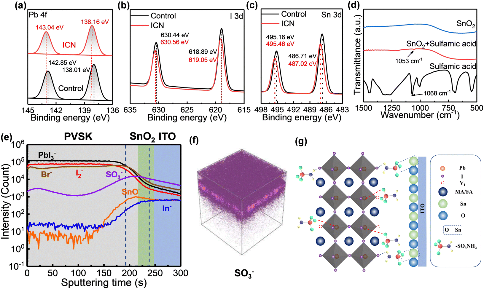 | ||
| Fig. 2 (a) Pb 4f, (b) I 3d, and (c) Sn 3d XPS spectra. (d) Fourier transform infrared spectra of SnO2, sulfamic acid, and SnO2 with sulfamic acid modification. (e) ToF-SIMS depth profiles of the perovskite/SnO2/ITO/glass. The molecular fragments from the perovskite (PbI3−, I2−, and Br−), sulfamic acid (SO3−), SnO2 (SnO−), and ITO (In−) are shown. (f) The 3D rendered overlay images of the SO3− signals for samples with ICN modification. (g) The schematic illustration of the chemical interaction mechanism of ICN with the perovskite layer and the SnO2 layer. | ||
To further demonstrate the effect of sulfamic acid on PbI2, we carried out XRD measurements on the sulfamic acid powder and “PbI2 + sulfamic acid” for characterizing the chemical interaction. Several characteristic diffraction peaks for the sulfamic acid powder can be observed in the XRD patterns. As shown in Fig.S7(b) (ESI†), various diffraction peaks at low angles were detected for PbI2 mixed films with a molar ratio of 1![[thin space (1/6-em)]](https://www.rsc.org/images/entities/char_2009.gif) :1. The diffraction peaks from this non-perovskite complex belong neither to sulfamic acid nor to PbI2. This further indicates that H+(NH2–SO3)− undergoes a chemical coordination with PbI2, mainly due to the coordination of sulfamic acid with Pb2+, which is similar to the coordination mechanism between DMSO and PbI2 reported in previous studies. Combined with the XPS results, we can infer that PbI2 does indeed coordinate with sulfamic acid to form complexes.
:1. The diffraction peaks from this non-perovskite complex belong neither to sulfamic acid nor to PbI2. This further indicates that H+(NH2–SO3)− undergoes a chemical coordination with PbI2, mainly due to the coordination of sulfamic acid with Pb2+, which is similar to the coordination mechanism between DMSO and PbI2 reported in previous studies. Combined with the XPS results, we can infer that PbI2 does indeed coordinate with sulfamic acid to form complexes.
To study the interaction of sulfamic acid on SnO2, we carried out the XPS measurement and FTIR measurement. The binding energy peak of Sn 3d shifted from 495.16 eV and 486.71 eV to 495.46 eV and 487.02 eV, respectively (Fig. 2c), indicating the interaction between sulfamic acid and SnO2. From the FTIR spectrum of sulfamic acid powder, the peak of the symmetric stretching vibration of SO in sulfamic acid was observed at 1068 cm−1, while the sulfamic acid-modified SnO2 layer presents a SO stretching vibration peak at 1053 cm−1 obviously (Fig. 2d). This shift of SO peaks proves the interaction between sulfamic acid and SnO2. In conclusion, sulfamic acid can simultaneously coordinate with the Pb2+ of PbI2/perovskite and Sn4+ in SnO2 to modulate crystal growth. Furthermore, the –NH2 in sulfamic acid can interact with the halogen atoms through hydrogen bonds (Fig. 2g). The effect of hydrogen bonds is to introduce heterogeneous nucleation sites and hinder crystal growth. The heterogeneous nucleation sites lower the nucleation energy barrier and thus increase the nucleation rate.31 This dual effect leads to the formation of loose-packing large-sized PbI2 porous films.
We also performed ToF–SIMS measurements and investigated the cross-sectional distribution of sulfamic acid on the ITO/SnO2/Perovskite (ICN) samples. As shown in Fig. 2(e) and (f), –SO3− confirms the existence and distribution of sulfamic acid. The region with the highest intensity of the –SO3− characteristic peak is located between the perovskite layer and the SnO2 layer. Most of the sulfamic acid is distributed at the interface, some sulfamic acid has penetrated the entire SnO2 layer and a small amount into the perovskite layer. The above results indicate that most sulfamic acid could act as interfacial molecules chemically anchored at the SnO2/perovskite interface. In summary, sulfamic acid can not only regulate the morphology of PbI2 but also control the crystallization process of the perovskite. At the same time, an interfacial chemical bridge is constructed between SnO2 and the perovskite by the sulfamic acid-based ICN strategy, as is exhibited in the detailed schematic diagram of the chemical reaction mechanism in Fig. 2g.
We constructed planar PSCs without and with ICN modification, and the device configuration of ITO/SnO2/Perovskite (ICN)/spiro-OMeTAD/Au is shown in the cross-sectional SEM images in Fig. 3(a) and (b). The current density–voltage (J–V) curves of the champion devices based on FAxMA1−xPb(IyBr1−y)3 and FAPbI3 are presented in Fig. 3(c) and (d). The control device based on FAxMA1−xPb(IyBr1−y)3 exhibited a peak PCE of 21.09% (a JSC of 24.95 mA cm−2, a VOC of 1.127 V, and an FF of 76.87%). In contrast, the ICN-modified device exhibited an improved maximum PCE of 22.41% (a JSC of 25.21 mA cm−2, a VOC of 1.141 V, and an FF of 77.84%). Particularly, the champion device with ICN modification exhibited a maximum PCE of 23.08% (a JSC of 25.47 mA cm−2, a VOC of 1.154 V, and an FF of 78.51%). It can be seen that the VOC and JSC of the devices are significantly enhanced, which is mainly attributed to the effective passivation of the interfacial and bulk defects of the perovskite films by ICN modification. Fig. S8 (ESI†) shows the direct relationship between the operating time at the maximum power measurement and the stable output current density and PCE for the control and ICN-modified devices. The ICN-modified device could maintain a stable output current density of 23.27 mA cm−2 and an output PCE of 20.90% after 200 seconds, while the control device only had an output current density of 20.40 mA cm−2 and an output PCE of 19.46%.
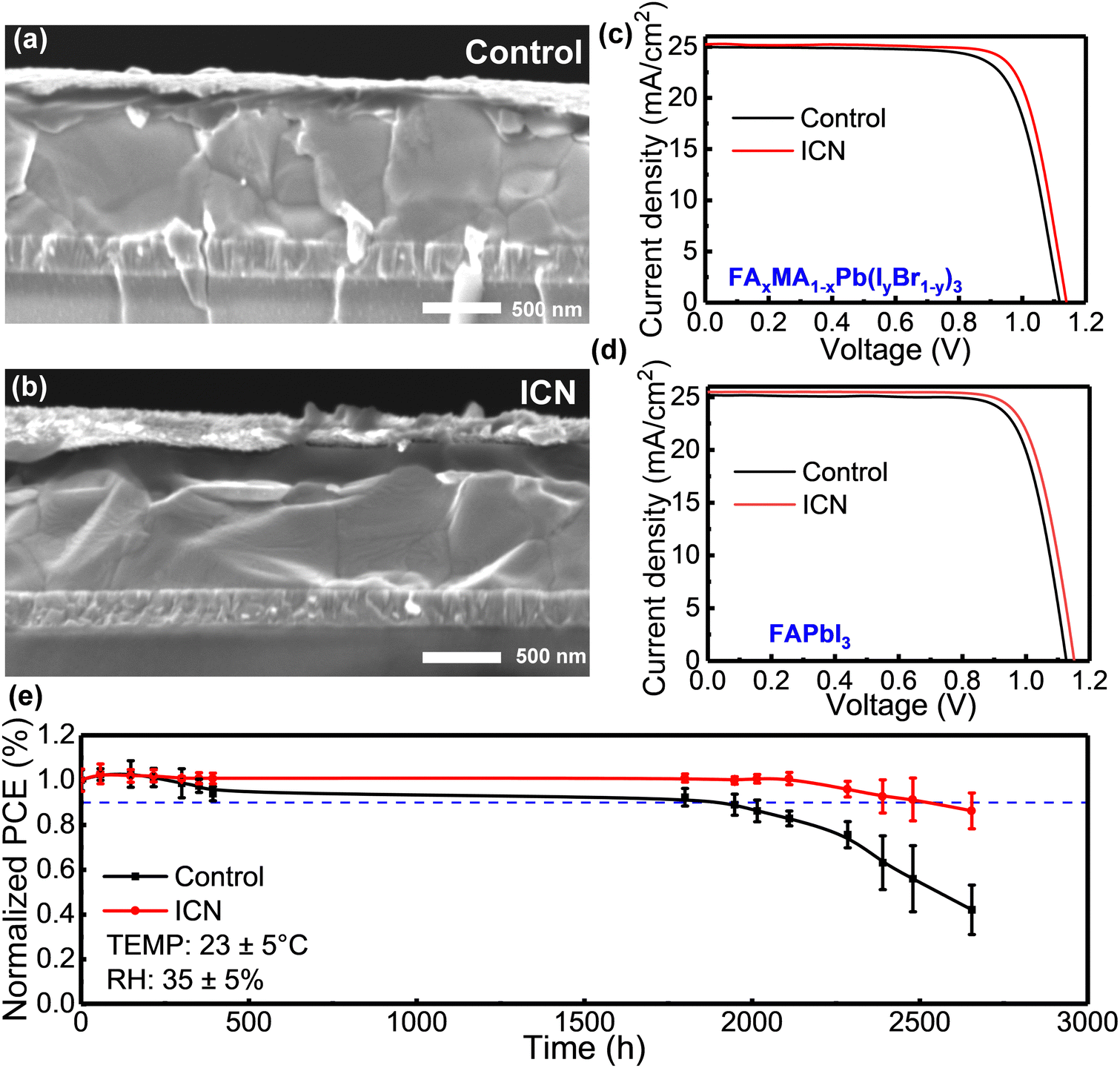 | ||
| Fig. 3 Cross-sectional SEM images of the (a) control and (b) the ICN-modified devices. J–V curves of the champion control and ICN-modified PSCs based on (c) FAxMA1−xPb(IyBr1−y)3 and (d) FAPbI3, two kinds of the photoactive layer. (e) Normalized PCE values of PSCs under ambient conditions with RH = 35 ± 5%. | ||
To investigate the effect of ICN on the stability of the perovskite films and the corresponding PSC devices, we first investigated the effect of ICN on the moisture stability of the perovskite films by placing the films in an environment with a temperature of 23 ± 5 °C and a relative humidity (RH) of 80% ± 5%, and the morphological changes are shown in Fig. S9 (ESI†). We can observe that the control perovskite film is almost completely degraded in 28 days, while in contrast, the ICN-modified perovskite film could retain its black photoactive phase for 28 days. The XRD patterns showed that the control film exhibited a characteristic peak at 12.7° of PbI2 that was elevated on the seventh day (Fig. S10, ESI†), and a faint peak attributed to δ-FAPbI3 appeared at 11.7°.32 Both PbI2 and δ-FAPbI3 phases are degradation products, indicating the significantly decomposed perovskite. After 26 days, there was almost no perovskite on the film, but only the yellow phase and PbI2 existed. In contrast, the ICN-modified perovskite films did not change significantly on the seventh and sixteenth days. A certain degree of the perovskite phase was still maintained on day 26, indicating that the ICN-modified perovskite crystal structure exhibits a high degree of integrity and structural stability. Meanwhile, the UV-vis absorption intensity recorded for the control films decreased significantly with time, while that of the ICN-modified films decreased only slightly (Fig. S11, ESI†).
We also tracked the device efficiency exceeding 2600 h at RH = 35 ± 5%. The ICN-modified devices can maintain more than 91% of their initial performance after 2500 h (Fig. 3e). Thus, ICN-modified perovskite films and devices showed significantly improved environmental stability. The enhanced film stability and device stability are mainly due to the following reasons, including (i) the chemical interaction of –NH2 in ICN with halides connected by hydrogen bonds, which stabilizes the Pb–I octahedral framework and inhibits the phase change of the perovskite crystal structure. (ii) –SO3NH2 in ICN can effectively passivate uncoordinated Pb2+. By the multiple effects, the defects in the perovskite films are effectively suppressed, and the active sites of degradation are reduced.
To investigate the effect of interface modification on the enhanced carrier recombination for PSC devices by ICN, we subsequently carried out the Mott–Schottky measurement and electrochemical impedance spectroscopy (EIS) measurement to analyze the carrier dynamics. The Mott–Schottky measurement (Fig. 4a) illustrates the larger built-in potential Vbi upon ICN modification and hence better carrier extraction and transport characteristics.33,34 EIS measurements illustrate a smaller charge transport resistance (Rct) and a larger recombination resistance (Rrec) of the ICN-modified devices compared with the control (Fig. 4b), which will contribute to the improvement of VOC.23 The ICN-modified perovskite devices have a lower current density (Fig. S12a, ESI†), which indicates that ICN effectively passivates the defects in the perovskite films.
 | ||
| Fig. 4 (a) Mott–Schottky plots of the control and ICN-modified PSCs. (b) Nyquist plots of the control and ICN-modified PSCs. (c) Dark I–V curves of the hole transport layer-only devices. (d) VOC as a function of light intensities for the devices based on the control and ICN-modified PSCs. (e) SSPL and (f) TRPL spectra of the control and the ICN-modified perovskite films on glass. KPFM of the (g) control and (h) ICN-modified perovskite films. (i) Contact potential difference along the lines of (g) and (h). | ||
We also performed the space charge-limited current (SCLC) method to quantify the passivating effect of ICN on the defects in the perovskite. The I–V curves under dark conditions for the dual hole transport layer devices are presented in Fig. 4c. The trap state density can be calculated from the trap filling limit voltage (VTFL) derived from the measurement according to the following equation
 | (1) |
We performed the light intensity-dependent VOC measurement. The relationship between the VOC and the light intensity of the device is shown in Fig. 4d. The slope of the control device is 1.56 KBT e−1, while the slope of the device with ICN modification is 1.13 KBT e−1. The lower slope corresponds to a less defect-assisted carrier recombination in the device.36 Combined with the enhanced steady-state photoluminescence (SSPL) intensity and the increased carrier lifetime from time-resolved photoluminescence spectroscopy (TRPL) approaching 7.23 μs for the ICN-modified perovskite films on the bare glass substrate, we conclude that ICN modification could help to improve crystallinity, passivate defects and suppress nonradiative recombination37 (Fig. 4(e), (f) and Table S3, ESI†).
To understand the mechanism of VOC enhancement, we used Kelvin probe force microscopy (KPFM) to probe the contact potential difference (CPD) of the control and ICN-modified perovskite film, as is presented in Fig. 4(g) and (h). The CPD is calculated to be the difference between the work function of the tip (Φtip) of the KPFM probe and that of the surface of the sample (Φsample). The CPD value (VCPD) between the tip and the sample is defined as VCPD = (Φtip − Φsample)/−e. It can be seen that ICN-modified film can exhibit an overall higher surface potential distribution. Precisely, the average CPD value is −211.21 mV for the control perovskite film, while it is −306.21 mV for the ICN-modified perovskite film, reflecting the deeper surface of the ICN-modified perovskite film potential (Fig. 4i). Since the KPFM measurement uses zero potential methods to record the volt potential value, we could deduce that the work function of perovskite upshifts 0.095 eV after ICN modification, which aligns with the enhanced VOC of PSC devices. Combined with UPS analysis results, the Fermi energy levels of the control and ICN-modified perovskite films are obtained to be −4.653 eV and −4.803 eV, respectively, while the valence band edges are −5.61 eV and −5.69 eV (Fig. S13, ESI†). The downward shift of the Fermi energy level is consistent with the changed CPD value in KPFM. Considering the bandgap values of 1.559 eV and 1.555 eV for the control and ICN-modified perovskite from the UV–Vis absorption measurement (Fig. S6 and S13(c), ESI†), respectively, we can conclude that ICN modification could induce perovskite films with a deeper CBM (Fig. S13, ESI†) for reducing the carrier recombination in the perovskite with the hole transport layer. Moreover, the Fermi energy level of the ICN-modified perovskite films is closer to the valence band edge, which leads to the enhancement of the hole extraction ability and facilitates the VOC improvement.
The impact of the ICN strategy on the crystallization of PbI2 and perovskite and the role of defect regulation can further expand its optoelectronic device applications. We further explored the potential of the ICN strategy for applying it to self-powered perovskite photodetectors with a typical photovoltaic device structure of ITO/SnO2/Perovskite (ICN)/spiro-OMeTAD/Au to characterize and analyze the light response characteristics. We first carried out an external quantum efficiency (EQE) measurement, which is the main index of a photodetector, and its value is the ratio of the number of photogenerated carriers to the incident photons at a given wavelength.38 The ICN-modified photodetectors show a higher EQE (Fig. 5a), which further illustrates the beneficial effect on the crystallization quality of the perovskite films. The I–V curves measured in the dark and under white light illumination (Fig. S14, ESI†) indicate that the ICN-modified photodetectors could exhibit a lower dark current density in the dark compared to the control photodetectors.
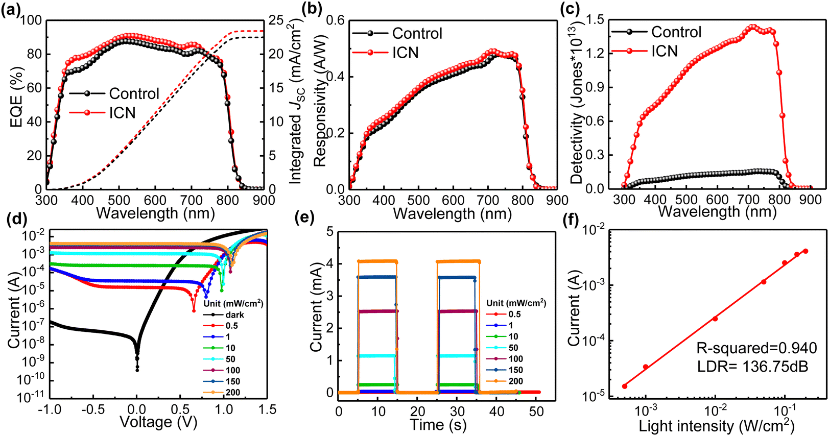 | ||
| Fig. 5 (a) EQE, (b) responsivity, and (c) detectivity of the control and photodetectors with ICN modification under 0 V bias. (d) I–V curves of the photodetector with ICN modification under different light intensities. (e) I–T curves of the photodetector with ICN modification under various light intensities under 0 V bias. (f) Power-dependent photocurrent under 0 V bias for the photodetector with ICN modification. | ||
Responsiveness (R) and detectability (D*) are also key performance indicators for photodetectors, which we calculated and shown in Fig. 5(b) and (c).39R is a measure of the index of the output produced by the detection of the input unit optical power signal, which can be expressed using the following equation40
 | (2) |
 | (3) |
To evaluate the dependence of photocurrent and photovoltage on the incident light intensity, we constructed I–V curves for different intensities of the incident light. As shown in Fig. 5d, the photocurrent is more sensitive than the photovoltage since the photocurrent is linearly related to the number of photogenerated carriers, whereas the photovoltage is mainly due to energy band bending or Fermi energy level fixation.42Fig. 5e shows the plots of the photocurrent (under 0 V bias, also called self-powered) for different light intensities (0.5, 1, 10, 50, 100, 150, and 200 mW cm−2), from which we can infer that the photocurrent increases proportionally with increasing light intensity. The photodetector also needs to have a constant response over a wide range of light intensities, and the LDR characterizes the range of light intensities over which the photodetector has constant responsiveness, which is calculated using the following equation: LDR = 20log(Ip/Id), where Ip and Id are the photocurrent and the dark current, respectively. By linearly fitting the data, the R squared value is calculated and fitted to be 0.940, close to the ideal factor of 1 (Fig. 5f). This result indicates an excellent linear relationship between the photocurrent and the light intensity in this measurement region, corresponding to an LDR of at least 136.75 dB, which is higher than that of the control photodetector (Fig. S15 and S16, ESI†).
The response speed reveals the detecting ability to track the incident light signal and has been another crucial parameter for photodetectors.39 As shown in Fig. 6a, a mechanical rotating chopper for light response speed measurements was used to control the incident frequency of the laser. The response speed of the photodetectors extracted at different wavelengths (760 nm and 810 nm) of the incident light are presented in Fig. 6(b), (c) and Fig. S17 (ESI†), respectively. It can be seen that the ICN-modified photodetectors have better stability and reproducibility. The transient response speed and the transient signal rise/fall of the photodetector were faster for the ICN-modified photodetectors. The result further confirms the defect passivation effect of ICN on perovskite films. In addition, we further obtain the rise time (τrise is defined as the response time for reaching 90% of the steady state value) and the fall time (τfall is defined as the response time drop to 10% of the steady state value) of the photodetectors. As shown in Fig. 6(b) and (c), the ICN-modified photodetector exhibited τrise and τfall values of 13 and 11 ms under a 760 nm light source, respectively, while the control photodetector showed τrise and τfall values of 26 and 16 ms, respectively. Simultaneously, the ICN-modified photodetector shows τrise and τfall values of 21 and 18 ms under an 810 nm light source, respectively, while the control photodetectors show τrise and τfall values of 27 and 20 ms respectively. The above results prove a faster response rate for the near-infrared light response, which has profound significance for the future implementation in NIR optical detection. The high-speed response data substantiate that the perovskite with ICN modification exhibits fewer defects and lower charge recombination.
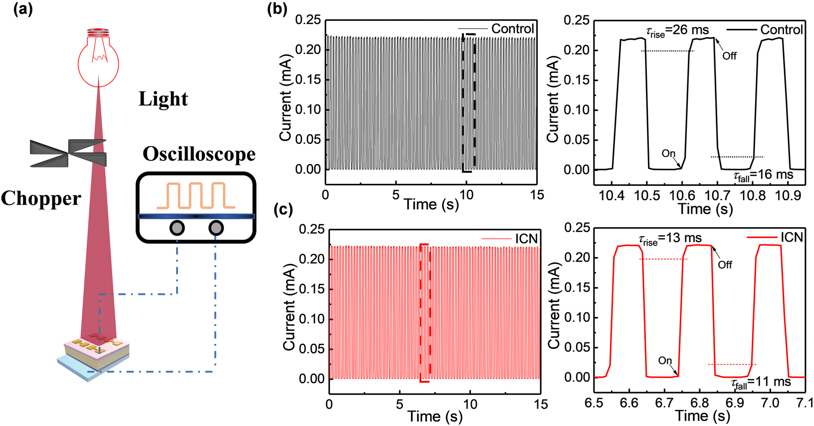 | ||
| Fig. 6 (a) A schematic diagram of the light response speed test of self-powered photodetectors. The photocurrent response curves of (b) the control and (c) ICN-modified photodetectors under a 760 nm light source, respectively. The corresponding rise and decay times from the enlarged photocurrent response curve of photodetectors are shown on the right side. | ||
Conclusion
In conclusion, a sulfamic acid-based ICN strategy was developed to modulate the porous morphology of PbI2 to obtain high-quality perovskite films using the typical sequential deposition route. Incorporating sulfamic acid into PbI2 could help to achieve a porous morphology, which will promote the adequate reaction of PbI2 with organic ammonium salts. Sulfamic acid, as a passivation agent, could interact with Pb2+ through coordination bonding and retard the crystallization of the PbI2 film with considerable grains and multiple pinholes. The sulfamic acid-based ICN strategy could also passivate the deep energy level defects and improve the photovoltaic performance of devices. As a result, the ICN-modified PSCs device without encapsulation could achieve a champion PCE of 23.08%, simultaneously maintaining 91% of its initial PCE after 2500 hours under ambient conditions in a high RH = 35 ± 5% environment. Furthermore, the ICN-modified photodetectors show responsivity values of up to 0.49 A W−1, with the D* value of 1.43 × 10¹³ and linear dynamic ranges of up to 136.75 dB. This strategy provides a universal method for improving the morphology of PbI2 and, thus, the quality of perovskite films for achieving efficient and reproducible perovskite photovoltaics.Experimental section
Materials
The SnO2 colloidal solution (15% in a H2O colloidal dispersion) was purchased from Alfa Aesar. Dimethyl sulfoxide (DMSO, 99.8%), isopropanol (IPA, 99.9%), N,N-dimethylformamide (DMF, 99.9%) and sulfamic acid (98%) were obtained from Macklin. Lead iodide (PbI2, 99.99%) and methylammonium chloride (MACl, 99.9%) were purchased from Xi’an Polymer Light Technology Corp. Formamidinium iodide (FAI, 99.9%) and methylammonium bromide (MABr, 99.9%) were obtained from Greatcell Solar Materials. Spiro-OMeTAD (99.5%) was purchased from Advanced Election Technology Co., Ltd. 4-tert-Butylpyridine and lithium bis-(trifluoromethylsulfonyl)imide (Li-TFSI) were purchased from Aladdin. All the reagents and chemicals were used without further purification.Device fabrication
First, ITO-coated glass substrates were cleaned with a glass cleaner, deionized water and anhydrous alcohol for 15 min. The substrates were dried in N2 and then modified by UV–O3 for 15 min. Then, SnO2 films were fabricated by spin-coating the precursor solution (1 mL of the SnO2 colloid precursor was diluted with 6 mL of deionized water) on the ITO substrates at 4000 rpm for 30 s and then annealed on a hot plate at 150 °C for 15 min under ambient conditions. After annealing, the ITO/SnO2 substrates were modified using UV–O3 for 15 min. The perovskite films were deposited through a two-step solvent engineering method. The 1.5 M PbI2 precursor solution was prepared in a mixed solvent of DMF and DMSO (900:100, volume ratio). After that, this precursor solution was spin-coated on the ITO/SnO2 substrate at 1500 rpm for 30 s, and annealed at 70 °C for 1 min. For comparison, 0.5 mg mL−1 sulfamic acid was doped into the PbI2 solution. For the perovskite film based on FAxMA1−xPb(IyBr1−y)3 deposition, a solution of FAI:MABr:MACl (90 mg:9 mg:9 mg in 1 mL of IPA) was spin-coated on PbI2 at a spin-coating rate of 1700 rpm for 30 s. For the perovskite film based on FAPbI3 deposition, a solution of FAI:MACl (90 mg:15 mg in 1 mL of IPA) was spin-coated on PbI2 at a spin rate of 1800 rpm for 30 s, and then the perovskite precursor film was quickly taken out from a nitrogen glove box to ambient air for thermal annealing at 150 °C for 15 min under humidity conditions (30–40% humidity). The hole transporting layer was prepared by spin-coating the Spiro-OMeTAD solution at 4000 rpm for 30 s. The spiro-OMeTAD solution (1 mL) was prepared by dissolving 72.3 mg of Spiro-OMeTAD, 17.5 μL of Li-TFSI solution (520 mg dissolved in 1 mL of acetonitrile), and 28.8 μL of 4-tert-butylpyridine in 1 mL of chlorobenzene. Finally, 100 nm of Ag or Au was deposited on the Spiro-OMeTAD-based hole transporting layer in a vacuum chamber using a thermal evaporator.
Device characterization
X-ray diffraction (XRD) patterns of the films were obtained using a Rigaku SmartLab using Cu Kα target radiation (λ = 1.5405 Å) with a power of 4 kW at a scanning rate of 10° min−1. The cross-sectional view of the device and the surface morphology of the films were scanned using a field-emission SEM (JEOL 7610F) with a voltage of 3 kV. The SSPL and TRPL were measured with fluorescence spectrometers (FLS1000). The absorption spectra were measured in the range from 300 to 900 nm using a Shimadzu UV-1800 spectrometer at a medium-speed scanning rate. AFM topography and KPFM were measured using an Agilent 5500 scanning probe microscope in tapping mode. ESCALAB 250Xi equipment was utilized for XPS measurements. Mott–Schottky measurements were carried out using an AMETEK VersSTAT 3F electrochemical workstation at a fixed frequency of 1000 Hz with bias voltage ranging from 0 to 1.5 V. EIS measurement was carried out in the dark with a frequency range from 0.1 Hz to 1000000 Hz using the same instrument as that used in the Mott–Schottky measurement under 0 V. J–V characterization was performed with a Keithley 2400 source measurement unit under simulated AM 1.5 irradiation (100 mW cm−2) using a standard xenon lamp-based solar simulator, which was calibrated using a standard silicon solar cell provided by PV Measurements Inc. J–V characterization was performed in a reverse scan (1.2 V → 0 V, step 0.05 V). UPS spectra were recorded using a PHI5000 VersaProbe III Spectrometer. EQE measurement was carried out using a QE-IRIS of Enlitech. Fourier transform infrared (FTIR) spectra were recorded using a Bruker Vertex 80V FTIR spectrometer.
Conflicts of interest
There are no conflicts to declare.Acknowledgements
This work was supported by the National Natural Science Foundation of China (62004058, U21A2076), the Natural Science Foundation of Hebei Province (F2020202022), State Key Laboratory of Reliability and Intelligence of Electrical Equipment (EERI_PI20200005), and the S&T Program of Hebei (215676146H, 225676163GH).Notes and references
- M. Li, H. Li, Q. Zhuang, D. He, B. Liu, C. Chen, B. Zhang, T. Pauporte, Z. Zang and J. Chen, Stabilizing Perovskite Precursor by Synergy of Functional Groups for NiOx-Based Inverted Solar Cells with 23.5% Efficiency, Angew. Chem., Int. Ed., 2022, 61(35), e202206914 CAS.
- D. Gao, R. Li, X. Chen, C. Chen, C. Wang, B. Zhang, M. Li, X. Shang, X. Yu and S. Gong, et al., Managing Interfacial Defects and Carriers by Synergistic Modulation of Functional Groups and Spatial Conformation for High-Performance Perovskite Photovoltaics Based on Vacuum Flash Method, Adv. Mater., 2023, 35(23), 2301028 CrossRef CAS PubMed.
- J.-H. Im, C.-R. Lee, J.-W. Lee, S.-W. Park and N.-G. Park, 6.5% efficient perovskite quantum-dot-sensitized solar cell, Nanoscale, 2011, 3(10), 4088 RSC.
- H. Zhang, J. Mao, H. He, D. Zhang, H. L. Zhu, F. Xie, K. S. Wong, M. Grätzel and W. C. H. Choy, A Smooth CH3NH3PbI3 Film via a New Approach for Forming the PbI2 Nanostructure Together with Strategically High CH3NH3I Concentration for High Efficient Planar-Heterojunction Solar Cells, Adv. Energy Mater., 2015, 5(23), 1501354 CrossRef.
- Q. Jiang, Z. Chu, P. Wang, X. Yang, H. Liu, Y. Wang, Z. Yin, J. Wu, X. Zhang and J. You, Planar-Structure Perovskite Solar Cells with Efficiency beyond 21, Adv. Mater., 2017, 29(46), 1703852 CrossRef PubMed.
- Q. Jiang, Y. Zhao, X. Zhang, X. Yang, Y. Chen, Z. Chu, Q. Ye, X. Li, Z. Yin and J. You, Surface passivation of perovskite film for efficient solar cells, Nat. Photonics, 2019, 13(7), 460 CrossRef CAS.
- D. Gao, M. Li, L. Yang, C. Wang, X. Shang, X. Ma, C. Wu, B. Zhang, H. Song and C. Chen, 3-Ammonium Propionic Acid: A Cation Tailoring Crystal Structure of Hybrid Perovskite for Improving Photovoltaic Performance, ACS Appl. Energy Mater., 2021, 4(12), 14662 CrossRef CAS.
- H. Wang, F. Ye, J. Liang, Y. Liu, X. Hu, S. Zhou, C. Chen, W. Ke, C. Tao and G. Fang, Pre-annealing treatment for high-efficiency perovskite solar cells via sequential deposition, Joule, 2022, 6(12), 2869 CrossRef CAS.
- B. W. Park, N. Kedem, M. Kulbak, D. Y. Lee, W. S. Yang, N. J. Jeon, J. Seo, G. Kim, K. J. Kim and T. J. Shin, et al., Understanding how excess lead iodide precursor improves halide perovskite solar cell performance, Nat. Commun., 2018, 9(1), 3301 CrossRef PubMed.
- Y. Han, H. Xie, E. L. Lim and D. Bi, Review of Two-Step Method for Lead Halide Perovskite Solar Cells, Solar RRL, 2022, 6(6), 2101007 CrossRef CAS.
- J. Liang, X. Hu, C. Wang, C. Liang, C. Chen, M. Xiao, J. Li, C. Tao, G. Xing and R. Yu, et al., Origins and influences of metallic lead in perovskite solar cells, Joule, 2022, 6(4), 816 CrossRef CAS.
- T. J. Jacobsson, J. P. Correa-Baena, E. Halvani Anaraki, B. Philippe, S. D. Stranks, M. E. Bouduban, W. Tress, K. Schenk, J. Teuscher and J. E. Moser, et al., Unreacted PbI2 as a Double-Edged Sword for Enhancing the Performance of Perovskite Solar Cells, J. Am. Chem. Soc., 2016, 138(32), 10331 CrossRef CAS PubMed.
- H. Z. Qi Chen, T.-B. Song, S. Luo, Z. Hong, H.-S. Duan, L. Dou, Y. Liu and Y. Yang, Controllable self-induced passivation of hybrid lead iodide perovskites toward high performance solar cells, Nano Lett., 2014, 14(7), 4158 CrossRef PubMed.
- D. H. Cao, C. C. Stoumpos, C. D. Malliakas, M. J. Katz, O. K. Farha, J. T. Hupp and M. G. Kanatzidis, Remnant PbI2, an unforeseen necessity in high-efficiency hybrid perovskite-based solar cells?, APL Mater., 2014, 2(9), 091101 CrossRef.
- F. Liu, Q. Dong, M. K. Wong, A. B. Djurišić, A. Ng, Z. Ren, Q. Shen, C. Surya, W. K. Chan and J. Wang, et al., Is Excess PbI2 Beneficial for Perovskite Solar Cell Performance?, Adv. Energy Mater., 2016, 6(7), 1502206 CrossRef.
- L. Duan and A. Uddin, Defects and stability of perovskite solar cells: a critical analysis, Mater. Chem. Front., 2022, 6(4), 400 RSC.
- S. a Shor Peled, M. Perez, D. Meron, A. Osherov, V. Bulovic, E. A. Katz and Y. Golan, Morphology control of perovskite films: a two-step, all solution process for conversion of lead selenide into methylammonium lead iodide, Mater. Chem. Front., 2021, 5(3), 1410 RSC.
- Y. Zhao, F. Ma, Z. Qu, S. Yu, T. Shen, H. X. Deng, X. Chu, X. Peng, Y. Yuan and X. Zhang, et al., Inactive (PbI2)2RbCl stabilizes perovskite films for efficient solar cells, Science, 2022, 377(6605), 531 CrossRef CAS PubMed.
- K. Liang, D. B. Mitzi and M. T. Prikas, Synthesis and Characterization of Organic−Inorganic Perovskite Thin Films Prepared Using a Versatile Two-Step Dipping Technique, Chem. Mater., 1998, 10(1), 403 CrossRef CAS.
- C. Ran, W. Gao, N. Li, Y. Xia, Q. Li, Z. Wu, H. Zhou, Y. Chen, M. Wang and W. Huang, Facet-Dependent Control of PbI2 Colloids for over 20% Efficient Perovskite Solar Cells, ACS Energy Lett., 2018, 4(1), 358 CrossRef.
- Y. Wu, A. Islam, X. Yang, C. Qin, J. Liu, K. Zhang, W. Peng and L. Han, Retarding the crystallization of PbI2 for highly reproducible planar-structured perovskite solar cells via sequential deposition, Energy Environ. Sci., 2014, 7(9), 2934 RSC.
- G. Tumen-Ulzii, C. Qin, D. Klotz, M. R. Leyden, P. Wang, M. Auffray, T. Fujihara, T. Matsushima, J. W. Lee and S. J. Lee, et al., Detrimental Effect of Unreacted PbI2 on the Long-Term Stability of Perovskite Solar Cells, Adv. Mater., 2020, 32(16), e1905035 CrossRef PubMed.
- L. Zhu, X. Zhang, M. Li, X. Shang, K. Lei, B. Zhang, C. Chen, S. Zheng, H. Song and J. Chen, Trap State Passivation by Rational Ligand Molecule Engineering toward Efficient and Stable Perovskite Solar Cells Exceeding 23% Efficiency, Adv. Energy Mater., 2021, 11(20), 2100529 CrossRef CAS.
- Y. Zhao, Q. Li, W. Zhou, Y. Hou, Y. Zhao, R. Fu, D. Yu, X. Liu and Q. Zhao, Double-Side-Passivated Perovskite Solar Cells with Ultra-low Potential Loss, Solar RRL, 2019, 3(2), 1800296 CrossRef.
- S. Wang, C. Wu, H. Yao, L. Ding and F. Hao, The nonhalides in perovskite solar cells, Mater. Chem. Front., 2023, 7(5), 789 RSC.
- Y. Cui, C. Chen, C. Li, L. Chen, S. S. Bista, X. Liu, Y. Li, R. A. Awni, Z. Song and Y. Yan, Correlating Hysteresis and Stability with Organic Cation Composition in the Two-Step Solution-Processed Perovskite Solar Cells, ACS Appl. Mater. Interfaces, 2020, 12(9), 10588 CrossRef CAS PubMed.
- Y. Zhang, P. Gao, E. Oveisi, Y. Lee, Q. Jeangros, G. Grancini, S. Paek, Y. Feng and M. K. Nazeeruddin, PbI2-HMPA Complex Pretreatment for Highly Reproducible and Efficient CH3NH3PbI3 Perovskite Solar Cells, J. Am. Chem. Soc., 2016, 138(43), 14380 CrossRef CAS PubMed.
- Z. Xiong, X. Chen, B. Zhang, G. O. Odunmbaku, Z. Ou, B. Guo, K. Yang, Z. Kan, S. Lu and S. Chen, et al., Simultaneous Interfacial Modification and Crystallization Control by Biguanide Hydrochloride for Stable Perovskite Solar Cells with PCE of 24.4%, Adv. Mater., 2022, 34(8), e2106118 CrossRef PubMed.
- G. Dong, J. Ha, Y. Yang, L. Qiu, R. Fan, W. Zhang, L. Bai, W. Gao and M. Fu, 4-Tert butylpyridine induced MAPbI3 film quality enhancement for improving the photovoltaic performance of perovskite solar cells with two-step deposition route, Appl. Surf. Sci., 2019, 484, 637 CrossRef CAS.
- X. Deng, Z. Cao, Y. Yuan, M. Oliver Lam Chee, L. Xie, A. Wang, Y. Xiang, T. Li, P. Dong and L. Ding, et al., Coordination modulated crystallization and defect passivation in high quality perovskite film for efficient solar cells, Coord. Chem. Rev., 2020, 420, 213408 CrossRef CAS.
- X. Meng, J. Lin, X. Liu, X. He, Y. Wang, T. Noda, T. Wu, X. Yang and L. Han, Highly Stable and Efficient FASnI3-Based Perovskite Solar Cells by Introducing Hydrogen Bonding, Adv. Mater., 2019, 31(42), e1903721 CrossRef PubMed.
- S. Masi, A. F. Gualdrón-Reyes and I. Mora-Seró, Stabilization of Black Perovskite Phase in FAPbI3 and CsPbI3, ACS Energy Lett., 2020, 5(6), 1974 CrossRef CAS.
- W. Yang, R. Su, D. Luo, Q. Hu, F. Zhang, Z. Xu, Z. Wang, J. Tang, Z. Lv and X. Yang, et al., Surface modification induced by perovskite quantum dots for triple-cation perovskite solar cells, Nano Energy, 2020, 67, 104189 CrossRef CAS.
- F. Cai, J. Cai, L. Yang, W. Li, R. S. Gurney, H. Yi, A. Iraqi, D. Liu and T. Wang, Molecular engineering of conjugated polymers for efficient hole transport and defect passivation in perovskite solar cells, Nano Energy, 2018, 45, 28 CrossRef CAS.
- Y. Huang, L. Li, Z. Liu, H. Jiao, Y. He, X. Wang, R. Zhu, D. Wang, J. Sun and Q. Chen, et al., The intrinsic properties of FA(1−x)MAxPbI3 perovskite single crystals, J. Mater. Chem. A, 2017, 5(18), 8537 RSC.
- D. Yang, X. Zhou, R. Yang, Z. Yang, W. Yu, X. Wang, C. Li, S. Liu and R. P. H. Chang, Surface optimization to eliminate hysteresis for record efficiency planar perovskite solar cells, Energy Environ. Sci., 2016, 9(10), 3071 RSC.
- Q. Jiang, L. Zhang, H. Wang, X. Yang, J. Meng, H. Liu, Z. Yin, J. Wu, X. Zhang and J. You, Enhanced electron extraction using SnO2 for high-efficiency planar-structure HC(NH2)2PbI3-based perovskite solar cells, Nat. Energy, 2016, 2(1), 16177 CrossRef.
- V. O. Eze, G. R. Adams, L. Braga Carani, R. J. Simpson and O. I. Okoli, Enhanced Inorganic CsPbIBr2 Perovskite Film for a Sensitive and Rapid Response Self-Powered Photodetector, J. Phys. Chem. C, 2020, 124(38), 20643 CrossRef CAS.
- H. Zhou, J. Zeng, Z. Song, C. R. Grice, C. Chen, Z. Song, D. Zhao, H. Wang and Y. Yan, Self-Powered All-Inorganic Perovskite Microcrystal Photodetectors with High Detectivity, J. Phys. Chem. Lett., 2018, 9(8), 2043 CrossRef CAS PubMed.
- L. Dou, Y. M. Yang, J. You, Z. Hong, W. H. Chang, G. Li and Y. Yang, Solution-processed hybrid perovskite photodetectors with high detectivity, Nat. Commun., 2014, 5, 5404 CrossRef CAS PubMed.
- T. Klab, B. Luszczynska, J. Ulanski, Q. Wei, G. Chen and Y. Zou, Influence of PEIE interlayer on detectivity of red-light sensitive organic non-fullerene photodetectors with reverse structure, Org. Electron., 2020, 77, 105527 CrossRef CAS.
- L. J. A. Koster, V. D. Mihailetchi, R. Ramaker and P. W. Blom, Light intensity dependence of open-circuit voltage of polymer: fullerene solar cells, Appl. Phys. Lett., 2005, 86(12), 123509 CrossRef.
Footnote |
| † Electronic supplementary information (ESI) available. See DOI: https://doi.org/10.1039/d3qm00490b |
| This journal is © the Partner Organisations 2023 |