
 Open Access Article
 This Open Access Article is licensed under a Creative Commons Attribution-Non Commercial 3.0 Unported Licence
Simple approach for an electron extraction layer in an all-vacuum processed n-i-p perovskite solar cell†
Beom-Soo
Kim
*ab,
Daniel
Pérez-del-Rey
a,
Abhyuday
Paliwal
a,
Chris
Dreessen
 a,
Michele
Sessolo
a and
Henk J.
Bolink
*a
a,
Michele
Sessolo
a and
Henk J.
Bolink
*a
aInstituto de Ciencia Molecular, Universidad de Valencia, Calle Catedrático Jose Beltrán 2, Paterna, 46980, Spain. E-mail: henk.bolink@uv.es
bAdvanced Materials Division, Korea Research Institute of Chemical Technology (KRICT), Daejeon 34114, Korea. E-mail: bkim@krict.re.kr
First published on 16th March 2022
Abstract
Vacuum processing is considered to be a promising method allowing the scalable fabrication of perovskite solar cells (PSCs). In vacuum processed PSCs, the n-i-p structure employing organic charge transport layers is less common than the p-i-n structure due to limited options to achieve an efficient electron extraction layer (EEL) on indium tin oxide (ITO) with vacuum thermal evaporation. There are a number of specific applications where an n-i-p structure is required and therefore, it is of interest to have alternative solutions for the n-type contact in vacuum processed PSCs. In this work, we report an efficient vacuum deposited EEL using a mixture of conventional organic small molecules, C60 and bathocuproine (BCP). Incorporation of BCP into C60 does not result in conventional n-doping; however, we observed enhanced charge extraction, which significantly increased the power conversion efficiency (PCE) from 13.1% to 18.1% in all-vacuum processed PSCs. The C60:BCP mixed (co-sublimated) film most likely results in shifted energy levels leading to better alignment with the electrodes.
Introduction
Perovskite solar cells (PSCs) have emerged as a candidate for next generation photovoltaics owing to their rapid increase of power conversion efficiency (PCE) in the last decade, now exceeding 25%.1,2 The record efficiency of laboratory-scale PSCs is now higher than that of already commercialized solar cell technologies based on (Cu,In)GaSe2, CdTe, and amorphous Si and close to that of crystalline Si, and thus considerable interest has been generated for their commercialization.3–5 One of the pending issues for the industrial manufacture of PSCs is to identify a scalable fabrication process for the device stacks. So far, most of the reports on PSCs have shown fabrication with a spin coating-based solution process combined with high temperature annealing, which does not facilitate large area fabrications. A large-area solar module needs all the layers in the photovoltaic device to be deposited with scalable processes. Therefore, PSCs using scalable solution processes, such as blade coating, spray coating, inkjet printing and roll-to-roll printing, are being extensively studied.5–11 On the other hand, vacuum processing is one of the promising solutions for upscaling PSCs.12–14 Vacuum processing of thin films has several advantages, such as good process stability enabling large area, uniform films, and good control over the film depositions. Therefore, vacuum processed perovskites and all-vacuum processed PSCs have recently attracted considerable attention.12–24 In all-vacuum processed PSCs, the p-i-n structure is more commonly used than the n-i-p structure.17,18,22–27 This is related to the limited choice of materials for the interfacial layer, or contact layer between the electron extraction layer (EEL) and the electrode. In all-vacuum processed n-i-p devices, organic semiconductors have so far only scarcely been used for the n-interlayer. For example in 2015, Ke et al. reported an all-vacuum processed n-i-p PSC demonstrating a PCE of 14.5% using an intrinsic C60 layer contacted with fluorine-doped tin oxide (FTO).28 In 2016 and 2019, our group also reported all-vacuum processed n-i-p PSCs using novel n-type dopants, N1,N4-bis(tri-p-tolylphosphoranylidene)benzene-1,4-diamine (PhIm), and pentamethylcyclopentadienyl mesitylene ruthenium dimer, (RuCp*mes)2, co-evaporated with C60 demonstrating a PCE of 20.3% and 17.7%, respectively.29,30 In vacuum processed p-i-n PSCs, undoped C60 is the most widely used material for high efficiency devices. In this structure, the contact between C60 and the top metal electrode is usually optimized with an insertion of interfacial layers such as bathocuproine (BCP), bathophenanthroline (Bphen) or LiF with a top metal layer (e.g., Ag and Al).31–33 These interfacial layers, however, do not efficiently work on transparent conducting oxides (TCOs) such as indium tin oxide (ITO), since the mechanism of the improved contact using the interfacial layers requires the contact with the metal layers to form a metal complex.31–33 Hence, for n-i-p devices different solutions are needed. In particular, it was demonstrated that vacuum deposited CH3NH3PbI3 perovskite films on C60 showed a lower rate of trap assisted recombination than the perovskite film grown on an organic hole transporting material (HTM), (N4,N4,N4′′,N4′′-tetra([1,1′-biphenyl]-4-yl)-[1,1′:4′,1′′-terphenyl]-4,4′′-diamine, TaTm).34 In addition, vacuum processed PSCs have great potential for tandem application on silicon solar cells with a textured surface.35 A cost efficient and high performing silicon solar cell employs a tunneling oxide passivated contacts (TOPCon) structure, where an n-type silicon substrate with a boron (p+) emitter on the textured side has recently attracted much attention in industry.36,37 Hence, the vacuum processed n-i-p PSC could be significantly advantageous for the commercialization of high efficiency perovskite/Si tandem solar cells.38 These are the motivations to further develop vacuum processed n-i-p PSCs, as they have potential with high performing devices prepared with scalable processes. However, the previously reported organic n-dopants, PhIm and (RuCp*mes)2 are not widely used after their first report. Other conventional n-type dopants, such as Rb2CO3, Cs2CO3 and Ca could be alternative candidates to form an ohmic contact between ITO and C60.38 However, the processing and handling with these dopants is problematic due to their low ionization energy and tendency to decompose in vacuum processes.39–41 It is therefore of interest to develop efficient, low-temperature and vacuum-processable EELs for n-i-p structures based on materials that are stable and commercially available.In this work, we report on all-vacuum processed n-i-p PSCs, using C60 and BCP in the EEL deposited on ITO. We use the co-deposited C60 and BCP, C60:BCP mixed film, as an interfacial layer between ITO and an intrinsic C60 layer. In spite of the energy level distributions of BCP and C60, which do not allow n-type doping, surprisingly, the C60-BCP mixture layer significantly improved the contact between ITO and C60, resulting in an increase of the PCE from 13.1% (without the mixed layer) to 18.1%. We believe that our approach using conventional and vacuum-processable small organic molecules could promote the development of scalable n-i-p PSCs based on stable and low-cost materials.
Results and discussion
Fig. 1 shows the flat band energy diagram for the materials used in our n-i-p PSCs together with the molecular structure of organic semiconductors. Earlier, C60:BCP, or similarly C60:Bphen mixtures have been reported but mainly as an exciton blocking layer in organic photovoltaics (OPVs).42–44 However, in low bandgap perovskites, exciton blocking is not needed since free carriers are generated upon photoexcitation.45 In addition, it is important to note that the energy levels of C60 and BCP do not allow for conventional n-type doping, where an electron is transferred from the highest occupied molecular orbital (HOMO) of the dopants to the lowest unoccupied molecular orbital (LUMO) of the host. TaTm, 2,2′,2′′-(1,3,5-benzinetriyl)-tris(1-phenyl-1-H-benzimidazole) (TPBi) and molybdenum oxide (MoO3) are used as hole extraction layers (HELs) according to our previous report.46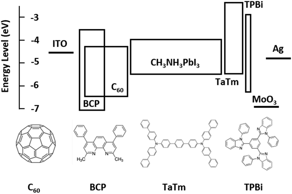 | ||
| Fig. 1 Energy diagram of the device and molecular structure of the organic materials. | ||
Fig. 2a shows the absorbance spectra of C60 films with different thicknesses, as well as for the co-evaporated C60:BCP mixed layers. C60 shows the expected absorption profile, with a band in between 400 and 550 nm, and higher absorbance at lower wavelengths. As the bandgap of BCP is very large (>3.5 eV), its optical absorption is negligible in the visible part of the spectrum. C60 is mainly responsible for the visible light absorption, and incorporation of BCP results in a negligible change in the films with 20 nm of C60 (the blue and green lines), and rather decreased in the films with 10 nm of C60 (the red and brown lines). This is originated from low n and k values of BCP which result in lower absorbance as shown in Fig. S2 (ESI†) using the transfer matrix optical model. The overall absorbance with the mixed layers at the given thicknesses is comparable with other typical organic hole extraction layers (HELs) and EELs.29,47Fig. 2b displays the conductivity of the intrinsic C60, the C60:BCP mixed layer, and the mixed film capped with an intrinsic C60 film. The conductivity experiments were done by evaporating the films on interdigitated ITO-coated glass substrates, and by measuring their current density vs. voltage characteristics. Due to the use of ITO as the electrodes, the measurements are affected by the mismatch between the ITO work function and the LUMO of the intrinsic C60 layer. The very low conductivity of the intrinsic C60 layer (∼10−9 to 10−8 S cm−1) (Fig. 2b) originates from the non-ohmic ITO/C60 interface. Interestingly, however, the conductivity is increased to 4 × 10⁻⁶ S cm−1 for the mixed C60:BCP layer and to 1.5 × 10⁻⁶ S cm−1 when intrinsic C60 is deposited on top of the mixed C60:BCP layer. These values are similar to the previously reported value for amorphous C60 films.43,48 As discussed, considering the energy levels of BCP and C60, the observed increase in conductivity is not due to an increase in the conductivity of C60:BCP, but rather is a result of the improved charge injection from the ITO electrode into the organic film.
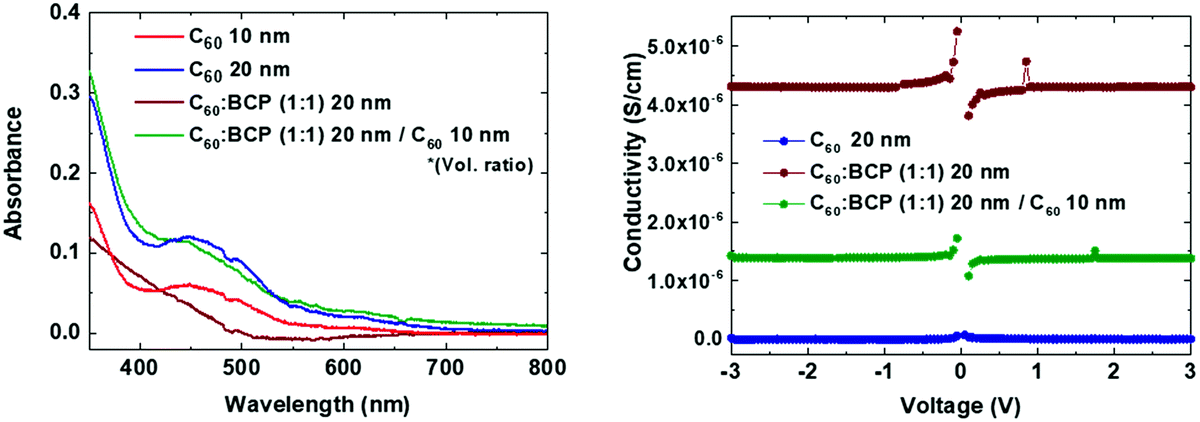 | ||
| Fig. 2 (a) Absorbance spectra and (b) conductivity vs. applied voltage of mixed C60:BCP and pure C60 films. | ||
C60![[thin space (1/6-em)]](https://www.rsc.org/images/entities/char_2009.gif) :BCP (ratio) :BCP (ratio) |
PCE (%) | V OC (V) | J SC (mA cm−2) | FF | R S (Ω cm2) |
|---|---|---|---|---|---|
| R S: Series resistance. | |||||
| 0.8:1.0 |
6.7 | 0.95 | 13.6 | 0.52 | 3.8 |
| 1.0:1.0 |
18.1 | 1.10 | 21.9 | 0.75 | 1.8 |
| 2.0:1.0 |
16.4 | 1.06 | 21.0 | 0.74 | 2.4 |
| 2.4:1.0 |
16.2 | 1.05 | 19.8 | 0.78 | 1.9 |
| C60 only (10 nm) | 13.1 | 1.08 | 15.7 | 0.66 | 2.1 |
To evaluate the charge injection/extraction characteristics of the C60:BCP mixed film as the EEL in PSCs, we fabricated n-i-p devices in which 20 nm thick films with different ratios of C60:BCP were deposited. As shown in Fig. 3a, the composition of the C60:BCP mixed films is as follows: C60:BCP = 0.8:1.0, 1.0:1.0, 2.0:1.0 and 2.4:1.0. As demonstrated in Fig. 3b, without the C60:BCP mixed layer (C60 only), the current density–voltage (J–V) curve shows a low fill factor and current density resulting in a PCE of 13.1%. When we introduce BCP in the mixed films (C60:BCP = 0.8:1.0), the solar cell performance is further reduced, leading to a PCE of 6.7%. Interestingly, however, when the C60:BCP ratio in the mixed films is adjusted to 1:1 the PCE is strongly improved (18.1%). Increasing the amount of C60 in the mixed films to C60:BCP = 2.0:1.0 and 2.4:1.0, does not further increase the PCE value of the devices. In fact, the PCE decreased to 16.4% and 16.2%, respectively. The mechanism of the enhanced device performance with the mixed layer is not clear. It seems unlikely that an increase in the carrier density due to a redox reaction between the two molecules is the cause as the energy levels do not support such a hypothesis. One potential explanation is that electrostatic interaction between C60 and BCP can cause shifts in their respective energy levels (e.g., the LUMO of C60), which enhances the injection/extraction property for the ITO contact. This is in line with a recent report that the energy levels of organic semiconductor molecules can be shifted in the mixed phase, including C60, via inter molecular electro-static interaction and structural orders.49–51
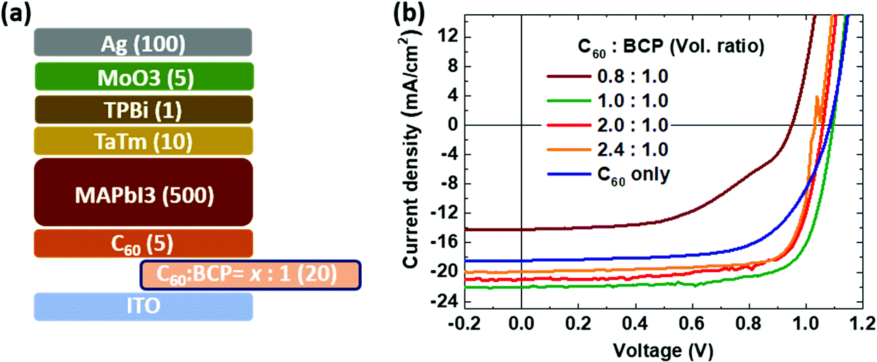 | ||
| Fig. 3 (a) Device configuration with different composition of the C60:BCP mixture (number in parenthesis represent the layer thickness in nm) and (b) the J–V curve under 100 mW cm−2 AM1.5 light illumination. | ||
We also examined the benefits of adding an intrinsic C60 layer in between the mixed C60:BCP layer for the device performance. The thicknesses of the C60 layer are varied from 0 (without the intrinsic layer), to 5 and 10 nm, and deposited on top of the mixed C60:BCP layer with the ratio 1.0:1.0. As shown in Fig. 4b, the device without the intrinsic C60 layer shows a very low PCE of 0.4%, caused primarily by the extremely low current level. As the thickness of the intrinsic C60 layer increases to 15 nm, the VOC is slightly enlarged (1.116 V), as well as the FF (0.78) when compared to the device with a 5 nm intrinsic C60 layer, however, the JSC is lowered due to the optical loss by the thick (15 nm) intrinsic C60 layer, which dominates and leads to a reduction in the PCE of 17.7%. The key performance data for the solar cells are depicted in Table 1. Therefore, we could confirm that the best condition shown previously, C60:BCP = 1:1 and 5 nm of intrinsic C60 layer is the optimized configuration for the n-i-p PSC. As shown in Fig. S3 (ESI†), for the device without the C60 layer on the C60:BCP = 2:1 mixed film, the PCE is much higher (15.1%) than the PCE of the 1:1 mixed film. From this result, we thus infer that in the 1:1 mixed film the top surface that is in contact with the perovskite layer is BCP-rich. As the electron affinity of BCP is significantly smaller than that of the perovskite, this leads to an electron extraction barrier leading to charge recombination at the interface between the BCP-rich surface and perovskite layer. This barrier is reduced with increasing C60 content in the mixed layer.
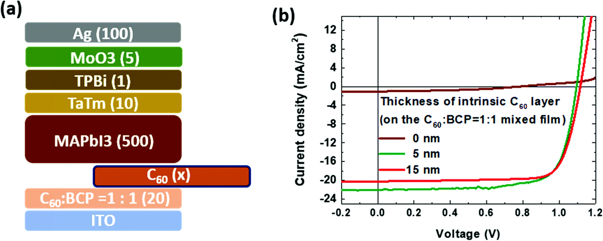 | ||
| Fig. 4 (a) Device configuration with different thickness of the intrinsic C60 layer and (b) the J–V curve under 100 mW cm−2 AM1.5 light illumination. | ||
To further investigate the origin of the enhanced device performance with the mixed layer, we measured the X-ray diffraction (XRD) and intensity dependent photoluminescence quantum yield (PLQY) of the perovskite films grown on ITO/C60 and ITO/C60:BCP/C60, as displayed in Fig. 5 (see ESI† for further details). The XRD patterns of CH3NH3PbI3 films on C60:BCP and C60:BCP/C60 are almost identical, as shown in Fig. 5a. Thus, it can be suggested that the improved performance of the device with the mixed layer is not attributed to differed growth of CH3NH3PbI3 films. The PLQYs of the perovskite films is also rather similar over a wide range of excitation intensities, from 0.08 to 20 Suns, for both types of interface layers. The similar PLQY values with a similar slope suggest that there are no significant differences in the interface recombination for both films.52,53 Hence, based on the datasets discussed above, it can be deduced that the improvement in the device performance using the mixed layer is more likely attributed to the energy level shift via electrostatic interaction and structural orders of organic semiconductors as previously reported.49–51
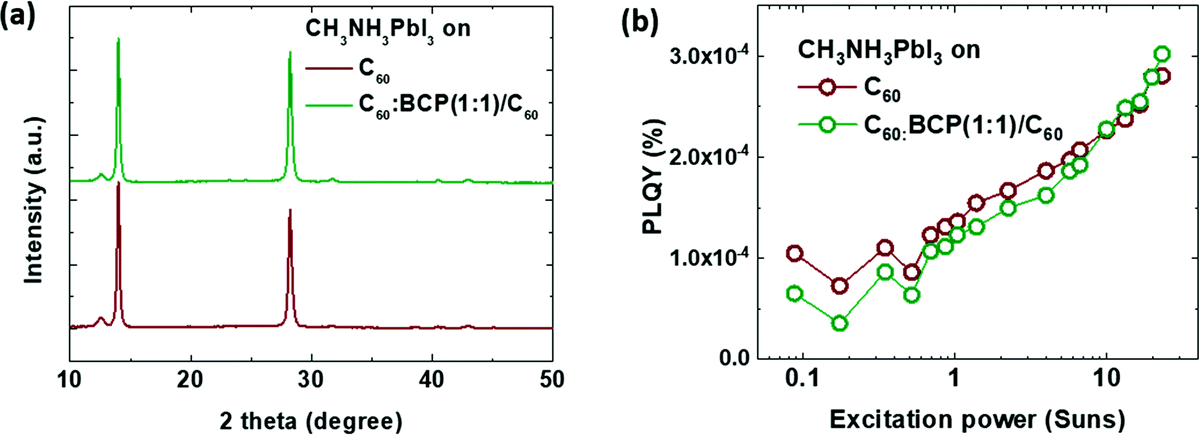 | ||
| Fig. 5 (a) X-Ray diffraction patterns of CH3NH3PbI3 films grown on ITO/C60 and ITO/C60:BCP/C60 and (b) photoluminescence quantum yield (PLQY) under different excitation powers. | ||
Conclusion
In conclusion, we demonstrated an efficient n-i-p PSC prepared using only vacuum deposition methods and employing a novel organic-molecule-based electron extraction layer. The electron extraction layer consists of a mixture of C60 and BCP, two well-known and commercially available electron transport molecules. The large band gap of BCP impedes conventional n-doping effects of C60; however, the mixed layer significantly promotes the charge extraction and leads to a PCE increase from 13% to 18%. We believe that the utilization of the organic mixture layer as an interfacial layer, as we demonstrated in this work, will be beneficial for other organic electronic devices.Conflicts of interest
There are no conflicts to declare.Acknowledgements
We acknowledge Jorge Ferrando for technical support. The research leading to these results has received funding from the European Research Council (ERC) under the European Union's Horizon 2020 research and innovation programme (Grant agreement No. 834431), Authors acknowledge support from the Comunitat Valenciana (IDIFEDER/2018/061 and PROMETEU/2020/077), as well as by the Ministry of Science and Innovation (MCIN), and the Spanish State Research Agency (AEI): Project PCI2019-111829-2 funded by MCIN/AEI/10.13039/501100011033 and by the European Union; Project PCI2020-112084 funded by MCIN/AEI/10.13039/501100011033 and by the “European Union NextGenerationEU/PRTR”; Project CEX2019-000919-M funded by MCIN/AEI/10.13039/501100011033. C. D. acknowledges that the project that gave rise to these results received the support of a fellowship from ‘‘la Caixa’’ Foundation (ID 100010434, code LCF/BQ/DI19/11730020). AP acknowledges his Grisolia grant from the Comunitat Valenciana (GRISOLIAP/2020/134).References
- A. Kojima, K. Teshima, Y. Shirai and T. Miyasaka, J. Am. Chem. Soc., 2009, 131, 6050–6051 CrossRef CAS PubMed
.
- NREL https://www.nrel.gov/pv/cell-efficiency.html.
- L. Meng, J. You and Y. Yang, Nat. Commun., 2018, 9, 5265 CrossRef CAS PubMed
- S. Albrecht and B. Rech, Nat. Energy, 2017, 2, 16196 CrossRef
- N.-G. Park and K. Zhu, Nat. Rev. Mater., 2020, 5, 333–350 CrossRef CAS
- H. Hu, Z. Ren, P. W. K. Fong, M. Qin, D. Liu, D. Lei, X. Lu and G. Li, Adv. Funct. Mater., 2019, 29, 1900092 CrossRef
- Y. Deng, X. Zheng, Y. Bai, Q. Wang, J. Zhao and J. Huang, Nat. Energy, 2018, 3, 560–566 CrossRef CAS
- M. Park, W. Cho, G. Lee, S. C. Hong, M. C. Kim, J. Yoon, N. Ahn and M. Choi, Small, 2019, 15, 1804005 CrossRef PubMed
- S. K. Karunakaran, G. M. Arumugam, W. Yang, S. Ge, S. N. Khan, X. Lin and G. Yang, J. Mater. Chem. A, 2019, 7, 13873–13902 RSC
- Y. Y. Kim, T.-Y. Yang, R. Suhonen, A. Kemppainen, K. Hwang, N. J. Jeon and J. Seo, Nat. Commun., 2020, 11, 5146 CrossRef CAS PubMed
- F. Huang, M. Li, P. Siffalovic, G. Cao and J. Tian, Energy Environ. Sci., 2019, 12, 518 RSC
- J. Li, H. Wang, X. Y. Chin, H. A. Dewi, K. Vergeer, T. W. Goh, J. W. M. Lim, J. H. Lew, K. P. Loh, C. Soci, T. C. Sum, H. J. Bolink, N. Mathews, S. Mhaisalkar and A. Bruno, Joule, 2020, 4, 1035 CrossRef CAS
- J. Ávila, C. Momblona, P. P. Boix, M. Sessolo and H. J. Bolink, Joule, 2017, 1, 431 CrossRef
- Y. Vaynzof, Adv. Energy Mater., 2020, 2003073, 2020 Search PubMed
- M. Liu, M. B. Johnston and H. J. Snaith, Nature, 2013, 501, 395–398 CrossRef CAS PubMed
- O. Malinkiewicz, A. Yella, Y. H. Lee, G. M. Espallargas, M. Graetzel, M. K. Nazeeruddin and H. J. Bolink, Nat. Photonics, 2014, 8, 128–132 CrossRef CAS
- L. E. Polander, P. Pahner, M. Schwarze, M. Saalfrank, C. Koerner and K. Leo, APL Mater., 2014, 2, 081503 CrossRef
- B.-S. Kim, T.-M. Kim, M.-S. Choi, H.-S. Shim and J.-J. Kim, Org. Electron., 2015, 17, 102–106 CrossRef CAS
- Q. Q. Lin, A. Armin, R. C. R. Nagiri, P. L. Burn and P. Meredith, Nat. Photonics, 2015, 9, 106–112 CrossRef CAS
- S. Wang, L. K. Ono, M. R. Leyden, Y. Kato, S. R. Raga, M. V. Lee and Y. Qi, J. Mater. Chem. A, 2015, 3, 14631–14641 RSC
- L. K. Ono, S. Wang, Y. Kato, S. R. Raga and Y. Qi, Energy Environ. Sci., 2014, 7, 3989–3993 RSC
- L. Gil-Escrig, C. Dreessen, F. Palazon, Z. Hawash, E. Moons, S. Albrecht, M. Sessolo and H. J. Bolink, ACS Energy Lett., 2021, 827–836 CrossRef CAS PubMed
- M. M. Tavakoli, P. Yadav, D. Prochowicz and R. Tavakoli, Sol. RRL, 2021, 5, 2000552 CrossRef CAS
- L. Gil-Escrig, C. Dreessen, I. C. Kaya, B.-S. Kim, F. Palazon, M. Sessolo and H. J. Bolink, ACS Energy Lett., 2020, 5, 3053 CrossRef CAS
- B.-S. Kim, L. Gil-Escrig, M. Sessolo and H. J. Bolink, J. Phys. Chem. Lett., 2020, 11, 6852–6859 CrossRef CAS PubMed
- A. Babaei, K. P. S. Zanoni, L. Gil-Escrig, D. Pérez-del-Rey, P. P. Boix, M. Sessolo and H. J. Bolink, Front. Chem., 2020, 7, 936 CrossRef PubMed
- R. Ji, Z. Zhang, C. Cho, Q. An, F. Paulus, M. Kroll, M. Löffler, F. Nehm, B. Rellinghaus, K. Leo and Y. Vaynzof, J. Mater. Chem. C, 2020, 8, 7725 RSC
- W. Ke, D. Zhao, C. R. Grice, A. J. Cimaroli, G. Fang and Y. Yan, J. Mater. Chem. A, 2015, 3, 23888–23894 RSC
- C. Momblona, L. Gil-Escrig, E. Bandiello, E. M. Hutter, M. Sessolo, K. Lederer, J. Blochwitz-Nimoth and H. J. Bolink, Energy Environ. Sci., 2016, 9, 3456–3463 RSC
- J. Avila, M.-G. La-Placa, E. Longhi, M. Sessolo, S. Barlow, S. R. Marder and H. J. Bolink, J. Mater. Chem. A, 2019, 7, 25796–25801 RSC
- Z. T. Xie, W. H. Zhang, B. F. Ding, X. D. Gao, Y. T. You, Z. Y. Sun, X. M. Ding and X. Y. Hou, Appl. Phys. Lett., 2009, 94, 063302 CrossRef
- H. Heil, J. Steiger, S. Karg, M. Gastel, H. Ortner, H. von Seggern and M. Stößel, J. Appl. Phys., 2001, 89, 420 CrossRef CAS
- H. Yoshida, J. Phys. Chem. C, 2015, 119, 24459 CrossRef CAS
- T. S. Sherkar, C. Momblona, L. Gil-Escrig, J. Ávila, M. Sessolo, H. J. Bolink and L. J. A. Koster, ACS Energy Lett., 2017, 2, 1214–1222 CrossRef CAS PubMed
- L. Gil-Escrig, M. Roß, J. Sutter, A. Al-Ashouri, C. Becker and S. Albrecht, Sol. RRL, 2021, 5, 2000553 CrossRef CAS
- A. Richter, R. Müller, J. Benick, F. Feldmann, B. Steinhauser, C. Reichel, A. Fell, M. Bivour, M. Hermle and S. W. Glunz, Nat. Energy, 2021, 6, 429–438 CrossRef CAS
- Y. Chen, D. Chen, C. Liu, Z. Wang, Y. Zou, Y. He, Y. Wang, L. Yuan, J. Gong, W. Lin and X. Zhang, Progr. Photovoltaics: Res. Applic., 2019, 27, 827 CrossRef CAS
- E. Aydin, J. Liu, E. Ugur, R. Azmi, G. T. Harrison, Y. Hou, B. Chen, S. Zhumagali, M. De Bastiani, M. Wang, W. Raja, T. G. Allen, A. Ur Rehman, A. S. Subbiah, M. Babics, A. Babayigit, F. H. Isikgor, K. Wang, E. Van Kerschaver, L. Tsetseris, E. H. Sargent, F. Laquai and S. De Wolf, Energy Environ. Sci., 2021, 14, 4377 RSC
- J. M. Kim, S. J. Yoo, C. K. Moon, B. Sim, J. H. Lee, H. Lim, J. W. Kim and J. J. Kim, J. Phys. Chem. C, 2016, 120, 9475–9948 CrossRef CAS
- B. D. Naab, S. Zhang, K. Vandewal, A. Salleo, S. Barlow, S. R. Marder and Z. Bao, Adv. Mater., 2014, 26, 4268 CrossRef CAS PubMed
- J. Zhao, Y. Cai, J.-P. Yang, H.-X. Wei, Y.-H. Deng, Y.-Q. Li, S.-T. Lee and J.-X. Tang, App. Phys. Lett., 2012, 101, 193303 CrossRef
- A. N. Bartynski, C. Trinh, A. Panda, K. Bergemann, B. E. Lassiter, J. D. Zimmerman, S. R. Forrest and M. E. Thompson, Nano Lett., 2013, 13, 3315 CrossRef CAS PubMed
- K. J. Bergemann, J. A. Amonoo, B. Song, P. F. Green and S. R. Forrest, Nano Lett., 2015, 15, 3994–3999 CrossRef CAS PubMed
- Q. Burlingame, B. Song, L. Ciammaruchi, G. Zanotti, J. Hankett, Z. Chen, E. Katz and S. Forrest, Adv. Energy Mater., 2016, 6, 1601094 CrossRef
- A. Miyata, A. Mitioglu, P. Plochocka, O. Portugall, J. T.-W. Wang, S. D. Stranks, H. J. Snaith and R. J. Nicholas, Nat. Phys., 2015, 11, 582 Search PubMed
- D. Perez-del-Rey, L. Gil-Escrig, K. P. S. Zanoni, C. Dreesen, M. Sessolo, P. B. Boix and H. J. Bolink, Chem. Mater., 2019, 31(17), 6945–6949 CrossRef CAS
- H. Lee, J. Y. Kim and C. Lee, Int. J. Photoenergy, 2012, 2012(1), 8 Search PubMed
- T. Asakawa, M. Sasaki, T. Shiraishi and H. Koinuma, J. Appl. Phys., 1995, 34, 1958 CrossRef CAS
- M. Schwarze, W. Tress, B. Beyer, F. Gao, R. Scholz, C. Poelking, K. Ortstein, A. A. Günther, D. Kasemann, D. Andrienko and K. Leo, Science, 2016, 352, 1446–1449 CrossRef CAS PubMed
- K. R. Graham, G. O. Ngongang Ndjawa, S. M. Conron, R. Munir, K. Vandewal, J. J. Chen, S. Sweetnam, M. E. Thompson, A. Salleo, M. D. McGehee and A. Amassian, Adv. Energy Mater., 2016, 6, 1601211 CrossRef
- S. Bag, P. Friederich, I. Kondov and W. Wenzel, Sci. Rep., 2019, 9, 12424 CrossRef PubMed
- M. Stolterfoht, V. M. Le Corre, M. Feuerstein, P. Caprioglio, L. J. A. Koster and D. Neher, ACS Energy Lett., 2019, 4, 2887 CrossRef CAS
- M. Stolterfoht, P. Caprioglio, C. M. Wolff, J. A. Márquez, J. Nordmann, S. Zhang, D. Rothhardt, U. Hörmann, Y. Amir, A. Redinger, L. Kegelmann, F. Zu, S. Albrecht, N. Koch, T. Kirchartz, M. Saliba, T. Unold and D. Neher, Energy Environ. Sci., 2019, 12(9), 2778–2788 RSC
Footnote |
| † Electronic supplementary information (ESI) available. See DOI: https://doi.org/10.1039/d1ya00084e |
| This journal is © The Royal Society of Chemistry 2022 |