
 Open Access Article
 This Open Access Article is licensed under a Creative Commons Attribution-Non Commercial 3.0 Unported Licence
Thin films of electron donor–acceptor complexes: characterisation of mixed-crystalline phases and implications for electrical doping†
Andreas
Opitz
 *a,
Giuliano
Duva
b,
Marius
Gebhardt
c,
Hongwon
Kim
c,
Eduard
Meister
c,
Tino
Meisel
a,
Paul
Beyer
a,
Valentina
Belova
b,
Christian
Kasper
d,
Jens
Pflaum
d,
Linus
Pithan
be,
Alexander
Hinderhofer
b,
Frank
Schreiber
*b and
Wolfgang
Brütting
*c
*a,
Giuliano
Duva
b,
Marius
Gebhardt
c,
Hongwon
Kim
c,
Eduard
Meister
c,
Tino
Meisel
a,
Paul
Beyer
a,
Valentina
Belova
b,
Christian
Kasper
d,
Jens
Pflaum
d,
Linus
Pithan
be,
Alexander
Hinderhofer
b,
Frank
Schreiber
*b and
Wolfgang
Brütting
*c
aInstitut für Physik, Humboldt-Universität zu Berlin, 10099 Berlin, Germany. E-mail: Andreas.Opitz@hu-berlin.de
bInstitut für Angewandte Physik, Universität Tübingen, 72076 Tübingen, Germany. E-mail: Frank.Schreiber@uni-tuebingen.de
cInstitut für Physik, Universität Augsburg, 86159 Augsburg, Germany. E-mail: Wolfgang.Bruetting@physik.uni-augsburg.de
dExperimentelle Physik VI, Julius-Maximilians-Universität Würzburg, 97074 Würzburg, Germany
eEuropean Synchrotron Radiation Facility, 38043 Grenoble Cedex 9, France
First published on 25th November 2021
Abstract
Electron donor–acceptor (EDA) complexes are of interest as low-band gap molecular semiconductors and as dopants for molecular semiconducting matrices. This contribution establishes a link between optical, structural and vibrational properties of EDA complexes as well as the electrical doping by them. We comprehensively characterise co-deposited films of the donors dibenzotetrathiafulvalene and diindenoperylene and the acceptors tetracyanonaphthoquinodimethane and its hexa-fluorinated derivative. All co-deposited donor:acceptor systems form mixed crystalline structures and the EDA complex is characterised by the complex-related absorption and X-ray scattering features. The absorption energies of the analysed EDA complexes cross the neutral-to-ionic boundary. The degree of charge transfer is determined by vibrational spectroscopy. Here, strong spatial anisotropy is found for the diindenoperylene containing complexes. The electrical transport measurements reveal an exponential relation between electrical conductivity and activation energy of transport for all complex-doped systems. We show with this result that doping via complexes has the same dominant activation process as doping via integer charge transfer, which is the separation of Coulombically bound charges. Our results are put in a broader context and we provide an outlook on future possibilities and research on EDA complexes.
Introduction
The characterisation of electron donor–acceptor (EDA) complexes‡ dates back to the middle of the last century when the interaction between benzene derivatives and iodine was studied.1 It was found that the position of a newly appearing low energy absorption feature depends on the ionisation energy (IE) of the aromatic hydrocarbon.2 Later, also the interactions between different aromatic hydrocarbons as donor (D) and acceptor (A) molecules were studied both experimentally and theoretically.3,4 Mainly planar aromatic hydrocarbons form EDA complexes due to the possibility for π-orbital overlap and π-stacking.5 A molecular EDA complex consists of two molecules with an energy level offset and a mutual π-orbital interaction between the occupied frontier molecular orbitals of the electron donor and the unoccupied frontier molecular orbitals of the electron acceptor, forming a bond much weaker than a covalent one. This π-orbital interaction leads to a new electronic transition detectable at energies lower than the respective optical transitions of D and A molecules, which is called charge transfer (CT) absorption.Concerning the energy level offset, the relative energy levels between D and A can be described as follows. The energy level offset between D and A can be distinguished into two cases, a staggered gap and a broken gap heterojunction (HJ). These two cases are shown schematically for isolated molecules or thin films before contact in Fig. 1a and b. The energy levels of D and A molecules in the staggered gap configuration (type-II HJ) are such that the energy of the highest occupied molecular orbital (HOMO) of D is located in between the energies of the lowest unoccupied molecular orbital (LUMO) and the HOMO of A and at the same time the LUMO energy of A is located between the HOMO and LUMO energies of D. The broken gap configuration (type-III HJ) is marked by the point that both energy levels of A are lying energetically deeper than the HOMO level of D.
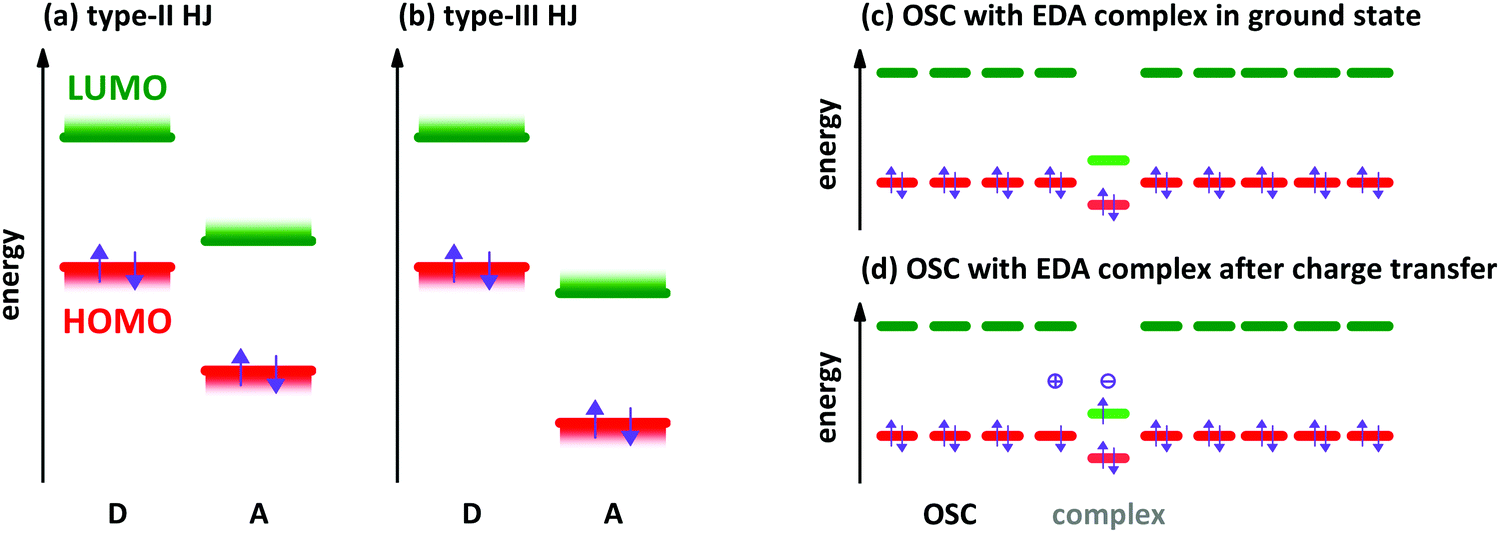 | ||
| Fig. 1 Schematic illustration of two relevant types of energy level alignment in the D/A heterojunctions (HJ) before contact of the materials: (a) type-II or staggered gap HJ, (b) type-III or broken gap HJ. Schematic energy levels of organic semiconductor (OSC) and EDA complex in the ground state (c) and after excitation (d) for the case of p-type doping. The violet arrows show the electron occupation of the molecular orbitals. The plus and minus signs illustrate the charged species after charge transfer. | ||
Depending on the molecular arrangement of D and A in the crystal structure, different electrical properties can be achieved.6–8 Alternating (or mixed) sequences of D and A molecules within a stack yield an insulating or semiconducting material. However, segregated stacks of equally spaced D and A molecules show high conductivities. Segregated stacks forming dimers along the stack are again insulating or semiconducting opening a gap due to a Peierls transition.6 Schematic representations of these stacks are given in Fig. 2.
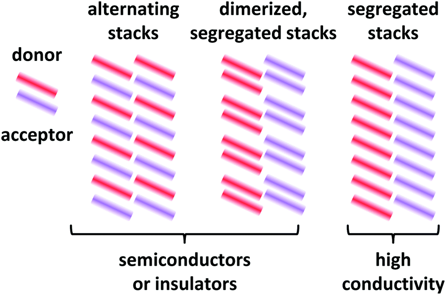 | ||
| Fig. 2 Schematic representations of EDA complex arrangements in mixed crystals. The coloured bars represent the donor and acceptor molecules. Only a 2D representation is used. | ||
The energy levels of the EDA complexes formed are mainly depending on the frontier orbitals of D and A molecules. Additionally, the knowledge of the crystal structure is fundamental for predictive calculations as the donor–acceptor interaction depends on the molecular arrangement and can strongly vary in different polymorphs.9–11 Even without knowledge of the detailed structure of the EDA complexes, some conclusions can be drawn from calculations based on density functional theory (DFT). Physical observables like IE and electron affinity (EA) depend on the different screening properties of the environment, i.e. these values differ for a single molecule in vacuum, for a molecule in a single-component film and for a molecule surrounded by a matrix of a different material, either of crystalline or amorphous nature.12–14 This has to be considered, e.g., for predicting electron or integer charge transfer (ICT) from inspection of energy levels determined by different experimental techniques15 and should also be taken into account for EDA complexes. Furthermore, geometric changes occur during charge transfer resulting in geometry-induced energy level shifts with a dependence of the CT character on the reorganisation energy.12,16 Based on these findings, the definition of a strongly coupled molecular system is given by the formation of an EDA complex, whereas weakly coupled molecular systems show ICT.16 The electronic and geometric structures of resulting EDA complexes are based on an interplay between electronic and geometric structure of the separated molecules as well as their electronic and steric interaction. Furthermore, the processing conditions are important since they determine for EDA complexes polymorphism and stoichiometric variations.9,17,18
EDA complexes can be regarded as low-gap organic semiconductors (OSC). DFT predicts mobility values of several tens of cm2 V−1 s−1 for electrons and holes along the D–A stacking direction comparable to single-component OSCs.19 However, the application in organic field-effect transistors gives lower mobility values for polycrystalline films and also for single crystal devices.9,20,21 The low gap offers the possibility to use EDA complexes as infra-red absorber for photovoltaics, photo-detectors and photo-thermal converters.22–24 EDA complex formation was found also in photovoltaic systems,25 where interaction between donor and acceptor is present only at the grain boundaries of separated D and A phases. The weakly absorbing EDA complex of zinc-phthalocyanine and fullerene C60 was used in infra-red detectors with optical cavities to increase the absorption of the complex.26 A hybrid complex-perovskite material was reported for photovoltaics, too.27 Furthermore, EDA complexes are used as dopants for OSCs,28,29 although the doping efficiency is lower than for redox- or acid–base doping with ICT.30,31 A schematic energy level diagram for an EDA complex as hole dopant in an OSC is given in Fig. 1c and d. The lower band gap of the complexes allows for higher probability of thermal excitation of an electron from HOMO to LUMO inside the complex than in the surrounding OSC. The OSC becomes p-doped after the transfer of an electron from the HOMO of the OSC to the empty site in the former HOMO of the complex. The electron transfer may also appear from the HOMO of the OSC directly to the LUMO of the CPX. This process has a lower energy barrier than the thermal activation inside the CPX. However, the spatial distance between the involved orbitals reduces the transition probability. By both ways, the EDA complex is negatively charged at the end (see Fig. 1d). The thermal excitation of the electron either inside the EDA complex or from OSC to the complex is described as the efficiency-limiting process for complex doping,30 as the separation of charges from the generated ion pairs to free charges in the OSC by overcoming the Coulomb attraction is present also in ICT doping.
In this manuscript we perform a comprehensive characterisation of EDA complexes using the donors dibenzotetrathiafulvalene (DBTTF) and diindenoperylene (DIP) as well as the acceptors tetracyanonaphthoquinodimethane (TCNNQ) and hexafluorotetracyanonaphthoquinodimethane (F6TCNNQ). The chemical structures are given in Fig. 3a. DBTTF is a strong donor and F6TCNNQ a strong acceptor molecule as given by oxidation and reduction potentials below. DIP and TCNNQ molecules show intermediate strength as donor and acceptor, respectively. The relevant oxidation and reduction potentials are summarized in Fig. 3b from previous publications as half-wave potentials.15,32,33 Type-III HJ is present only for the DBTTF:F6TCNNQ combination, all other combinations exhibit a type-II HJ. The CT absorption depends on the D and A redox potentials showing a neutral-ionic boundary. A comprehensive description of the EDA complexes formed in all of the mentioned D:A films will be given. This includes morphological and structural data as well as results from optical and vibrational spectroscopy. The relative energy levels and molecular size influences surface morphology, crystallinity, charge-transfer interaction and conductivity in co-deposited D:A films for all material combinations. Furthermore, the electrical conductivity upon complex doping shows thermally activated behaviour as reported before for ICT doping.
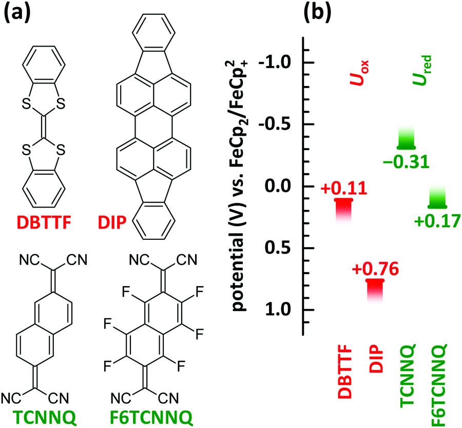 | ||
| Fig. 3 (a) Chemical structures of donor (DBTTF, DIP) and acceptor (TCNNQ, F6TCNNQ) molecules. (b) Oxidation potentials (Uox) of donor and reduction potentials (Ured) of acceptor materials determined by cyclic voltammetry.15,32,33 The oxidation potential for DIP is increased by 350 mV as given in ref. 33 considering the change of the standard potential due to the reported follow up reaction. | ||
Previously published data32,34–36 will be reconsidered and included in the discussion. To show the generality of our conclusions, the donor sexithiophene (6T) and the acceptor tetrafluorotetracyanoquinodimethane (F4TCNQ) will be included selectively.
Results
Charge transfer absorption and energy levels
First, we discuss the measurements of CT absorption features necessary to confirm the formation of EDA complexes in films containing D and A molecules. The CT absorption energies for co-deposited films of DBTTF and TCNNQ have already been reported.32 The existence of two different polymorphs (P1, P2) was suggested based on different CT absorption energies (0.72 eV, 0.84 eV) and different degrees of CT. The maximum of the absorption feature related to the DBTTF:F6TCNNQ EDA complex was determined to 1.43 eV.32 Additionally to the EDA complex absorption feature, ICT is present for the latter D:A pair, which is neglected for the discussion of EDA complexes.Absorption data of co-deposited films of DIP:TCNNQ and DIP:F6TCNNQ are shown in Fig. 4 measured at room temperature and at 77 K. For comparison the respective absorption data of single-component films are given. The CT absorption energy of the DIP:TCNNQ complex is 1.29 eV and for DIP:F6TCNNQ it is 0.97 eV, in agreement with ref. 35. Shifts of peak positions and changes of spectral features upon temperature variations are absent, indicating the absence of structural phase transitions in this temperature range. No signatures of DIP cation absorption or TCNNQ/F6TCNNQ anion absorption are present here.32,33 Therefore we exclude ICT in co-deposited films of DIP:TCNNQ and DIP:F6TCNNQ.
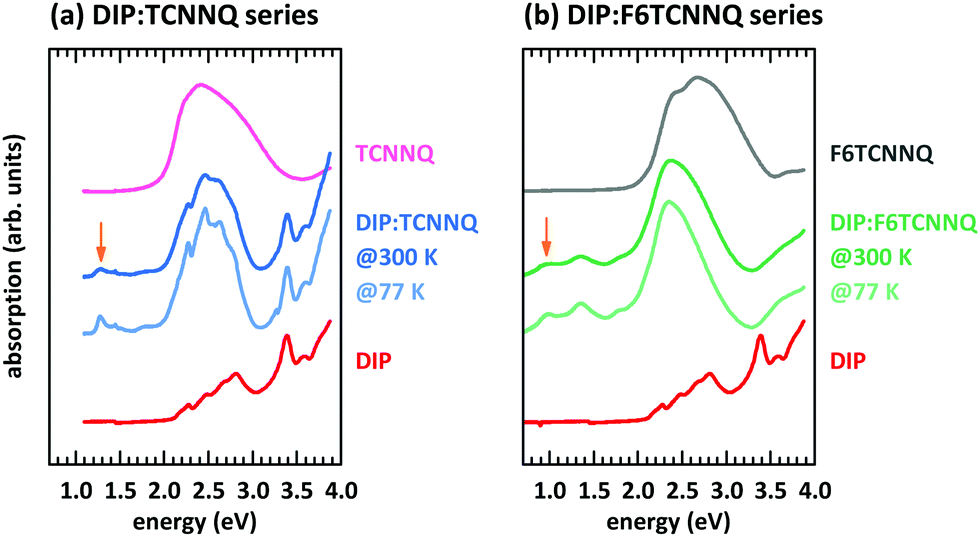 | ||
| Fig. 4 Absorption spectra for single component and equimolar co-deposited D:A films of DIP and TCNNQ (a) as well as of DIP and F6TCNNQ (b). The CT transitions are marked by orange arrows. The absorption spectra for co-deposited D:A were measured at 300 K and at 77 K. | ||
All mentioned systems form EDA complexes, as confirmed by the presence of a CT absorption. The related CT absorption energies ΔECPX are summarised in Table 1 (numbers 1–5) together with the intermolecular redox potential difference UDox − UAred.
Morphological and structural properties
So far, we have discussed EDA complexes without considering their crystalline structure. Important for a crystalline arrangement of EDA complexes is the π-orbital overlap between neighbouring D and A molecules as well as the details of electrostatic and van der Waals interactions. In this section we report on the surface morphology analysed by scanning force microscopy (SFM) and the molecular arrangement analysed by X-ray scattering techniques. We will start with DBTTF and continue with DIP as donor.The surface morphology of co-deposited D:A films containing DBTTF, TCNNQ and F6TCNNQ was discussed in a previous work.32 Single-component films of DBTTF are poly-crystalline with larger domains than the two single-component acceptor films. Low concentrations of TCNNQ in a co-deposited film preserves the DBTTF morphology, which may indicate a limited solubility of TCNNQ in DBTTF. Crystallites are present for higher TCNNQ concentrations, which were identified as mixed crystals. Co-deposited films of DBTTF and F6TCNNQ exhibit crystallites varying continuously between the size of the single-component films.
The presence of two polymorphs in DBTTF:TCNNQ co-deposited films was deduced from different transition energies of the CT absorption.32 Two polymorphs were also described for mixed crystals of DBTTF and the smaller acceptor TCNQ.9 Despite showing two distinct optical transitions, we note here that the difference in free energy for the formation of two polymorphs of the same D:A pairs can be small.37,38 Furthermore, the nucleation of these polymorphs might be induced by local inhomogeneities, by the presence of the substrate surface or subtle differences in the deposition rate.32,39 Here, we provide structural evidence for the coexistence of polymorphs P1 and P2 in DBTTF:TCNNQ mixed films. X-ray reflectivity (XRR) data for single-component films of DBTTF, TCNNQ and F6TCNNQ are displayed in Fig. 5. The DBTTF film shows (100) and (200) Bragg reflections, whereas such features are absent for the acceptor films. XRR data for co-deposited DBTTF:TCNNQ films are shown in Fig. 5a. The film of equimolar co-deposited DBTTF:TCNNQ named P1 is mainly consisting of this polymorph, whereas the other film contains both polymorphs. Preparation of pure P2 polymorph seems to be still challenging. The Bragg peak for the P1 polymorph can be identified and distinguished from the peak of the P2 polymorph. Furthermore, a new Bragg peak for co-deposited DBTTF:F6TCNNQ films can also be recognized (see Fig. 5b). The lattice spacings perpendicular to the substrate are estimated to be for DBTTF ≈ 13.6 Å, for DBTTF:TCNNQ P1 ≈ 13.0 Å, for DBTTF:TCNNQ P2 ≈ 12.1 Å, and for DBTTF:F6TCNNQ ≈ 14.2 Å. All these co-deposited films are forming EDA complexes, as shown by optical absorption measurements, and mixed crystals are present in films as demonstrated by the change of the lattice spacing compared to the single-component DBTTF film. Here the lattice spacing in the mixed crystals containing TCNNQ is smaller than the value for the single-component DBTTF film. In contrast, the lattice spacing is larger for the DBTTF:F6TCNNQ mixed crystal. This might be related to the size of the acceptor molecule or to different crystal packing induced by the different intermolecular and electronic couplings. The presence of two different polymorphs for the DBTFF:TCNNQ complexes was therefore confirmed by these measurements.32
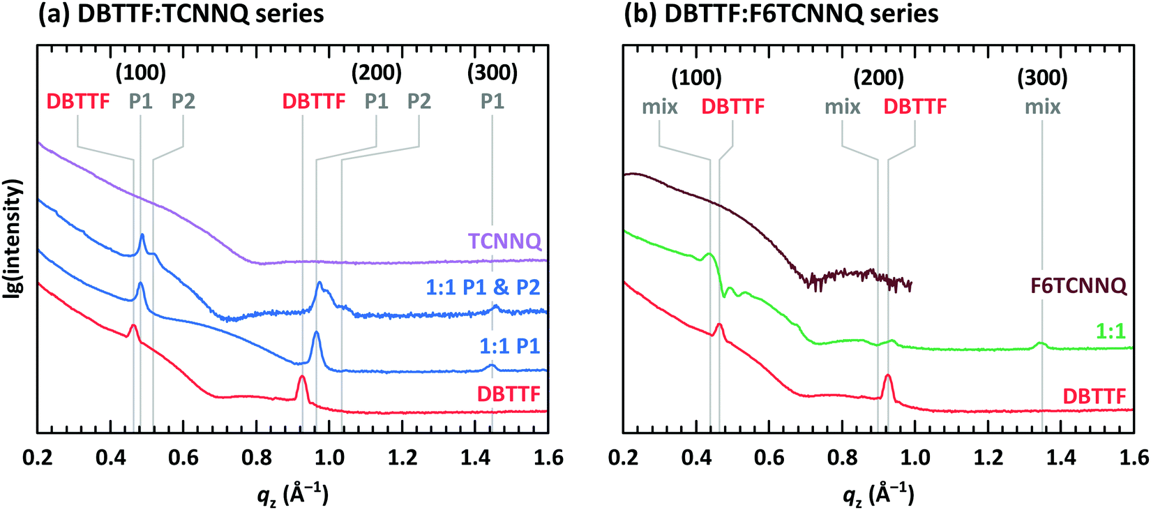 | ||
| Fig. 5 X-ray reflectivity measurements for single component and co-deposited films of (a) DBTTF and TCNNQ as well as of (b) DBTTF and F6TCNNQ. The Bragg peaks of the DBTTF thin film phase are marked together with the two polymorphs (P1, P2) for DBTTF:TCNNQ mixed crystals and with “mix” for the DBTTF:F6TCNNQ mixed crystal. The presence of the respective polymorphs in these co-deposited DBTTF:TCNNQ films was determined by optical absorption measurements. The data for the F6TCNNQ sample were measured only below 1.0 Å−1. | ||
The same samples investigated by XRR measurements were characterised by reciprocal space maps (see Fig. 6). The Bragg peaks for the DBTTF film (see Fig. 6a) are sharp and a pronounced 2D texture is present with low mosaicity. The combination of XRR and reciprocal space map data indicates the presence of the γ-polymorph of DBTTF.40 Extraction of unit cell parameters of this DBTTF thin-film polymorph becomes possible due to its well-defined crystalline texture. The resulting unit cell parameters are given in Table 2. For the neat acceptor films (see Fig. 6c and e), TCNNQ exhibits more pronounced diffraction peaks and 2D-texturing compared to F6TCNNQ. For TCNNQ, no single crystal structure has been reported so far. For F6TCNNQ, the crystal structure observed in thin films does not correspond to the reported one for single crystals34,41 and the few weak diffraction rings visible do not allow a reasonable guess.
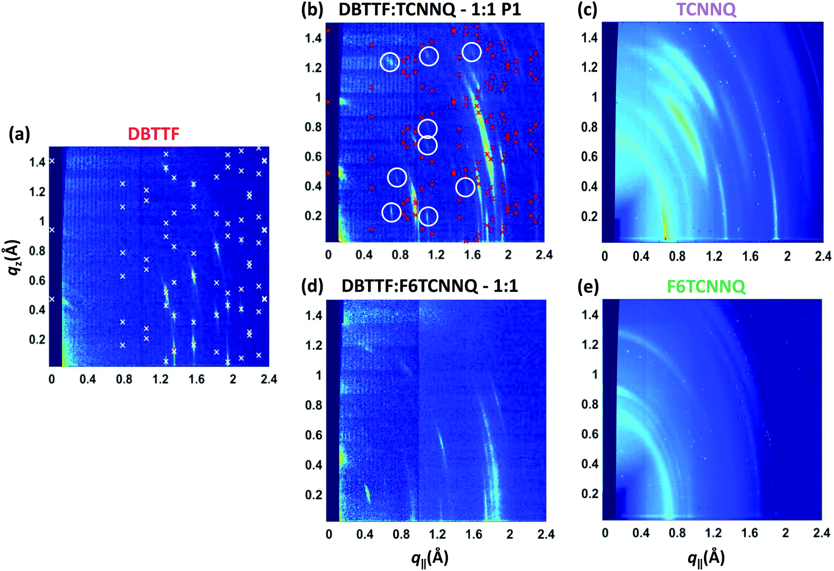 | ||
| Fig. 6 X-ray scattering reciprocal space maps for single component D and A films of DBTTF (a), TCNNQ (c) and F6TCNNQ (e) as well as for co-deposited D:A films of DBTTF:TCNNQ (b) and DBTTF:F6TCNNQ (d). The measurements were performed on the same samples as the XRR measurements in Fig. 5. The presence of the respective polymorphs in these co-deposited DBTTF:TCNNQ films was determined by optical absorption measurements. The X-ray diffraction pattern related to the calculated crystal structure solution of the DBTTF thin film phase and of the mixed crystal polymorph P1 in co-deposited DBTTF:TCNNQ films are marked by crosses. The circles mark weak diffraction peaks probably related to the much less abundant P2 polymorph, whose features however are not visible either in XRR or optical absorption spectra. The unit cell parameters are given in Table 2. The ring at qtot ≈ 0.7 Å−1 for the single component acceptor films stems from the Kapton window of the sample holder. | ||
| DBTTF | DBTTF:TCNNQ | ||
|---|---|---|---|
| Thin-film or γ-polymorph | Mixed crystal polymorph P1 | ||
| a | 6.02 Å | a | 13.24 Å |
| b | 8.05 Å | b | 7.66 Å |
| c | 13.90 Å | c | 13.84 Å |
| α | 100.29° | α | 105.86° |
| β | 99.90° | β | 75.95° |
| γ | 94.00° | γ | 100.93° |
| Volume | 649.09 Å3 | Volume | 1298.5 Å3 |
| Z | 2 | Z | 4 molecules 2 D:A pairs |
The measurement for the DBTTF:TCNNQ sample where predominantly the P1 polymorph is present shows an overall 2D-texture although with rather pronounced mosaicity. Part of the Bragg intensities measured by means of XRR is present in the reciprocal space map. This data allows also for estimation of the unit cell parameters, which are given in Table 2. In Fig. 6, Bragg peaks related to the fitted unit cell parameters are marked with crosses. The roughly doubled volume of the unit cell of the P1 polymorph in contrast to the γ-polymorph of DBTTF is related mainly to the roughly doubled a-parameter and points toward the presence of two crystallographically inequivalent EDA complexes in the unit cell. Additional Bragg peaks are highlighted by circles and do not belong to polymorph P1. Therefore, they are attributed to the polymorph P2, which seems to be present to a small extent here. However, the overall number of visible features for P2 is too low to extract the unit cell parameters with a reasonable initial guess. The respective reciprocal space map for the sample containing both polymorphs, P1 & P2, is given in ESI† (see Fig. S1). No peak assignment is possible for this data due to the nearly 3D powder-like thin film texture. Absorption measurements on this sample (also shown in Fig. S1 in ESI†) confirm the presence of both polymorphs.
The co-deposited DBTTF:F6TCNNQ film shows diffraction features being absent in the single-component films of DBTTF and F6TCNNQ (see Fig. 6). Comparing these results with the results presented from XRR measurements shows the presence of a mixed crystal formed by DBTTF and F6TCNNQ in agreement with conclusions from optical absorption data. A refinement of unit cell parameters is too prohibitive for this dataset. None of the reported structure of mixed crystals formed from DBTTF and FxTCNQ45,46 or from naphtho[1,2-b:5,6-b′]dithiophene and F6TCNNQ47 could provide a sufficient close initial guess for the fitting procedure to converge to a reasonable result. However, based on the qualitative similarity with the diffraction pattern of DBTTF:TCNNQ, here we cannot exclude the presence of two polymorphs with significantly different relative abundance.
Scanning force micrographs for single component DIP, TCNNQ and F6TCNNQ films are displayed in Fig. 7 together with micrographs of co-deposited D:A films. The RMS roughness values are given in the caption of Fig. 7. The single-component films show a homogeneous distribution of crystallites with the F6TCNNQ film exhibiting the highest roughness. Co-deposited films of DIP and TCNNQ exhibit smaller features than the respective single-component films. The equimolar film has a homogeneous surface morphology with roughness higher than the roughness of the respective single-component films. Small needle-like structures on top of a homogenous layer are present for the donor-rich DIP![[thin space (1/6-em)]](https://www.rsc.org/images/entities/char_2009.gif) :TCNNQ film (10:1) with an overall RMS roughness comparable to that of the single-component films of DIP and TCNNQ. The roughness of co-deposited DIP:F6TCNNQ films increase with the content of the acceptor between the roughness values for the respective single component films. Precipitations with different forms and sizes are present in these co-deposited films. Whereas large crystallites are visible for the 10:1 co-deposited film, smaller precipitations surrounded by a rather homogeneous phase are present for the equimolar film. Surface morphological features of the single-component films are absent in the co-deposited films in both series, indicating the absence of phase separation and the presence of mixed crystals.
:TCNNQ film (10:1) with an overall RMS roughness comparable to that of the single-component films of DIP and TCNNQ. The roughness of co-deposited DIP:F6TCNNQ films increase with the content of the acceptor between the roughness values for the respective single component films. Precipitations with different forms and sizes are present in these co-deposited films. Whereas large crystallites are visible for the 10:1 co-deposited film, smaller precipitations surrounded by a rather homogeneous phase are present for the equimolar film. Surface morphological features of the single-component films are absent in the co-deposited films in both series, indicating the absence of phase separation and the presence of mixed crystals.
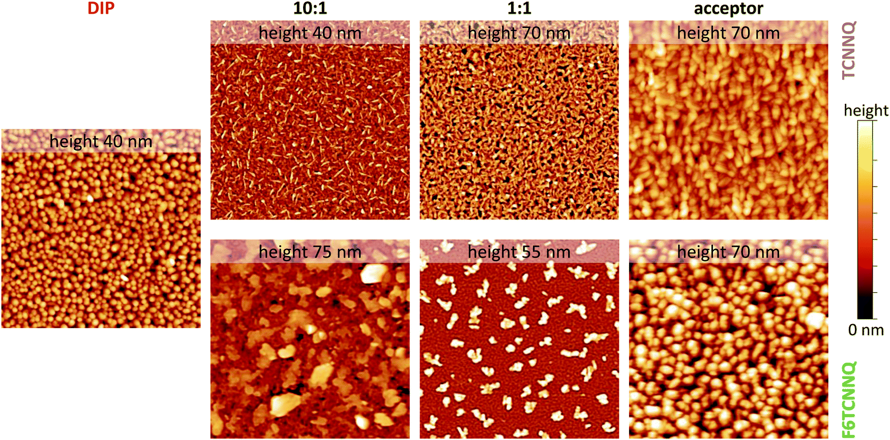 | ||
| Fig. 7 Scanning force microscopy images (4 × 4 μm2) for single-component and co-deposited D:A films of DIP, TCNNQ and F6TCNNQ. Different height scales are applied and the maximum of the scale is given (upper end of the colour bar at the right side, lower end corresponds to 0 nm). The root-mean square roughness values are 5.8 nm (DIP), 6.2/9.5 nm (10:1), 12.6/11.2 nm (1:1) and 8.2/15.2 nm (TCNNQ/F6TCNNQ), respectively. Image processing was performed using software package Gwyddion.48 | ||
XRR and grazing incidence X-ray diffraction (GIXD) data are shown in Fig. 8 for different molar ratios of co-deposited films of DIP and TCNNQ. Single-component DIP films consist of crystallites with upright standing molecules in the so-called σ-phase. Additionally, crystallites containing molecules lying down at the surface (λ-phase) are present on the co-deposited films as observed by GIXD measurements. Bragg peaks of the single-component TCNNQ film are present only in GIXD measurements.
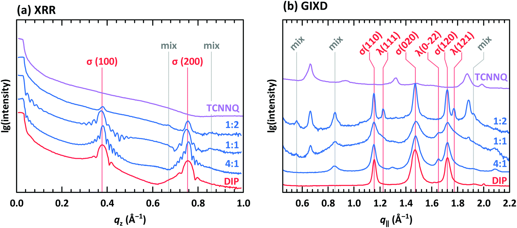 | ||
| Fig. 8 (a) X-ray reflectivity (XRR) and (b) grazing incidence X-ray diffraction (GIXD) measurements for single component and co-deposited films of DIP and TCNNQ. The peaks donated as σ(λ) are related to phases containing upright standing (lying) DIP molecules. Peaks marked as “mix” are attributed to the formed mixed crystal. Corresponding respective reciprocal space maps are shown in ESI† (see Fig. S1). | ||
The diffraction features of DIP are present also in co-deposited films with TCNNQ as observed from XRR and GIXD data. Pronounced Laue oscillations and Kiessig fringes are present for the DIP Bragg peaks in the films with molar ratios of 4:1 and 1:1 indicating a vertical coherence length virtually matching the entire film thickness. TCNNQ features are also present in GIXD for the co-deposited films showing the absence of order perpendicular to the substrate. Additional peaks present only in co-deposited films are related to the mixed crystal formed in these films, whose presence was deduced from optical absorption data (see Fig. 4a). Corresponding X-ray scattering reciprocal space maps are given in ESI† (see Fig. S2). The dominating presence of the DIP scattering features together with the presence of TCNNQ scattering features in the co-deposited films results from an overall tendency to phase-separation between donor and acceptor, although mixed crystals are still formed to some extent.
X-ray scattering data for co-deposited films of DIP and F6TCNNQ were presented in former studies.34,35 The formation of homogeneous crystalline domains of DIP:F6TCNNQ mixed crystals were observed for equimolar films. Diffraction features related to DIP gradually disappear by increasing the acceptor content in co-deposited films. At the same time, new Bragg peaks arise indicating the formation of DIP:F6TCNNQ mixed crystals in agreement with the results from absorption measurements.
The difference of DIP:TCNNQ (presented here) and DIP:F6TCNNQ (given in ref. 35) crystal structures seems to be related mainly to the different electronic structure of the acceptor molecule. The observed Bragg peaks are in similar wavevector regions and similar packing might be present. Such behaviour of similar molecular arrangement for different acceptors was observed before for TCNQ derivatives co-deposited with [1]benzothieno[3,2-b]benzothiophene (BTBT) and quaterthiophene (4T).28,29 In both series, the energy of the CT absorption shifts with the acceptor reduction potential, even though the overall appearance is quite similar. However, the absorption spectra for the DIP:TCNNQ and DIP:F6CTNNQ films are substantially different. Whereas one clear CT transition with vibronic progression is present for DIP:TCNNQ films, a second CT transition is present for DIP:F6TCNNQ films at about 1.35 eV. The pronounced double peak structure lead us to the conclusion that the electronic interaction might include more frontier orbitals than just HOMO and LUMO in the DIP:F6TCNNQ complex, whereas HOMO–LUMO interaction is mainly present for DIP:TCNNQ complexes.
Mixed crystals are formed in co-deposited films for all donor–acceptor combinations. The formation of solid solutions can be ruled out.49 The diffraction features of mixed crystals in co-deposited films are independent on their molar ratio, thus, the formation of ordered complexes seems to be obvious in this case. However, it is still unclear if the formation of mixed stacks or dimerized-segregated stacks is present. The presence of dimerized-segregated stacks was reported for mixed crystals of DBTTF and F4TCNQ,46 which are energetically and structurally close to the here studied DBTTF:F6TCNNQ co-deposited films, although in this case the different size of the acceptor molecule might play an important role in determining the exact arrangement and packing. Mixed stack ordered complexes were reported for combinations of F6TCNNQ with triphenyl, pyrene, phenanthracene, naphtho[1,2-b:5,6-b′]dithiophene47 or for BTBT, anthracene, carbazole, benzo[1,2-b:4,5-b′]dithiophene.50 On the basis of the presented data we assume that all shown EDA complex structures are referred to ordered complexes with mixed stacks, also called co-crystals. The strong CT absorption for DBTTF and F6TCNNQ co-deposited films might be a reason for the formation of other crystalline structures. These can be dimerized-segregated stacks, as reported for DBTTF and F4TCNQ46 as acceptor with comparable reduction potential, or the presence of ICT at grain boundaries.32 It has to be mentioned that a full solution of the crystal structure of all D:A pairs presented here is necessary to clarify the exact arrangements of the molecular stacks.
Vibrational properties and degree of charge transfer
Electron transfer to or from molecules changes their vibrational properties. Charge sensitive vibrations exhibit a strong shift of vibrational energy.51 The related energy change upon charging has to be larger than the possible change of polarizability of the environment arising from bringing donor and acceptor molecules in close contact. A degree of charge transfer of one is given for integer electron transfer. Thus, EDA complexes exhibit mainly a partial charge transfer or even no charge transfer. The vibrational energy varies in the simplest approach linearly with the degree of charge transfer.52 However, electron-molecular vibration coupling may play a substantial role, which needs to be considered with non-linear approaches to correctly model the dependence between shift of vibrational energy and degree of CT.53,54The analysis of the C![[triple bond, length as m-dash]](https://www.rsc.org/images/entities/char_e002.gif) N modes for some of the mentioned D:A systems has been measured before by means of infra-red absorption measurements.32,34 The two polymorphs P1 and P2 found for DBTTF:TCNNQ mixed crystals showed a degree of CT of 0.28 and zero, respectively. Co-deposited films of DBTTF and F6TCNNQ showed a mixed crystal with a degree of CT of 0.62 and a feature related to ICT. The later feature was attributed to disordered parts of the film at grain boundaries.32 Raman spectra of single-component and co-deposited D:A films for this material system are displayed in Fig. 9a. DBTTF exhibits a totally symmetric stretching vibrational mode of the central C
N modes for some of the mentioned D:A systems has been measured before by means of infra-red absorption measurements.32,34 The two polymorphs P1 and P2 found for DBTTF:TCNNQ mixed crystals showed a degree of CT of 0.28 and zero, respectively. Co-deposited films of DBTTF and F6TCNNQ showed a mixed crystal with a degree of CT of 0.62 and a feature related to ICT. The later feature was attributed to disordered parts of the film at grain boundaries.32 Raman spectra of single-component and co-deposited D:A films for this material system are displayed in Fig. 9a. DBTTF exhibits a totally symmetric stretching vibrational mode of the central C![[double bond, length as m-dash]](https://www.rsc.org/images/entities/char_e001.gif) C bond at about 1542 cm−1.55,56 This feature is marked by a vertical dashed line. The three other visible features of DBTTF are reported in literature without assignment.55,56 The Raman feature of the TCNNQ film at 1479 cm−1 is attributed to the C C ring stretching vibration.57 F6TCNNQ exhibits a feature at 1410 cm−1, which is described as CC in-plane stretching mode.47 The strong feature 1422 cm−1 was absent in this reference, which might be related to a different excitation energy. Resonant Raman excitation is more pronounced with the excitation energy of 2.33 eV used here.58
C bond at about 1542 cm−1.55,56 This feature is marked by a vertical dashed line. The three other visible features of DBTTF are reported in literature without assignment.55,56 The Raman feature of the TCNNQ film at 1479 cm−1 is attributed to the C C ring stretching vibration.57 F6TCNNQ exhibits a feature at 1410 cm−1, which is described as CC in-plane stretching mode.47 The strong feature 1422 cm−1 was absent in this reference, which might be related to a different excitation energy. Resonant Raman excitation is more pronounced with the excitation energy of 2.33 eV used here.58
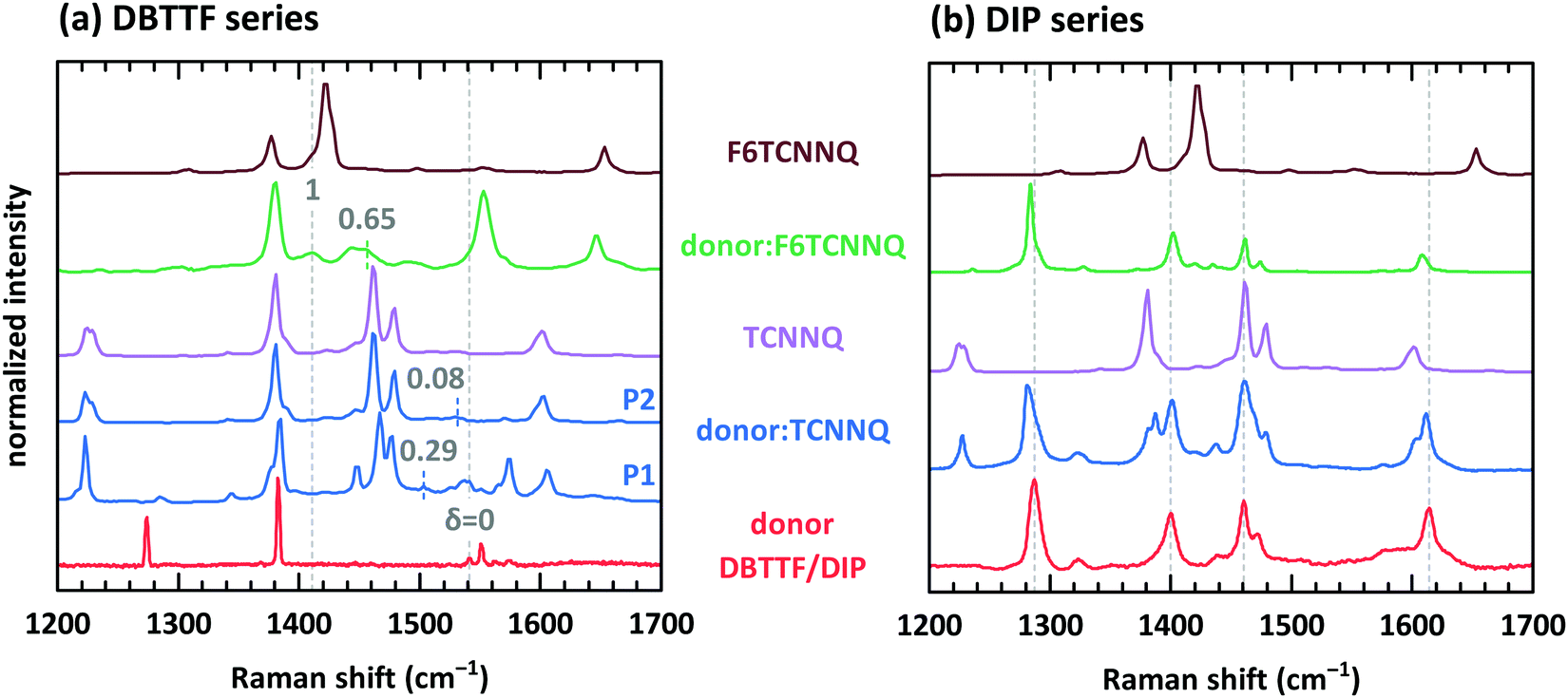 | ||
| Fig. 9 Raman spectra for single component and co-deposited films of DBTTF (a) and DIP (b) together with the spectra of TCNNQ and F6TCNNQ. Co-deposited films in the DIP series exhibit an equimolar ratio. Co-deposited films for the DBTTF series features a 10:1 molar ratio with a DBTTF excess (DBTTF:TCNNQ P1 and DBTTF:F6TCNNQ) or a equimolar ratio (DBTTF:TCNNQ P2). The grey, dashed lines in part (a) mark the symmetric stretching vibrational mode of the central CC bond in DBTTF for the neutral (δ = 0) and the charged (δ = 1) molecule.33,56,59 The coloured dashed lines give the estimated positions of this vibration in the co-deposited D:A films considering an linear change of the vibrational energy and the reported degree of charge transfer.32 These reported values are stated in the figure as well. The grey, dashed lines in part (b) mark the position of DIP vibrations assigned to in-plane vibrations as combination of CC stretching motion with C–H bending.58,60 | ||
New vibrational features are found in co-deposited D:A films. For analysing the charge transfer induced shifts, the focus will lay on the DBTTF mode at about 1542 cm−1. Related to this vibration the Raman shift changes by −38 and −10 cm−1 for films containing the polymorphs P1 and P2 of DBTTF:TCNNQ mixed crystals, respectively. The co-deposited film of DBTTF and F6TCNNQ displays new features with a change in the Raman shift of −85 and −130 cm−1. The later change corresponds to the change observed for the transition from neutral DBTTF to the DBTTF cation.33,55,56 Taking this shift as reference for ICT and radical ion state formation, the other feature in the co-deposited DBTTF:F6TCNNQ film corresponds to the EDA complex. The estimated degrees are 0.29 and 0.08 for the P1 and P2 polymorphs of DBTTF:TCNNQ, respectively. The EDA complex DBTTF:F6TCNNQ exhibits a degree of CT of 0.65. These values are in good agreement with the data reported on these EDA complexes determined from the CN stretching mode by infra-red transmission spectroscopy32 and determined from Raman measurements as shown in ESI† (see Fig. S3). A comparison of the observed shift of the CN stretching from Raman and infra-red spectroscopy is given in ESI† (see Table S1). All measurements (Raman spectroscopy on donor modes, Raman spectroscopy on CN mode, infra-red spectroscopy on CN mode) agree with each other (see also Table S1, ESI†). The data are summarised in Table 3.
| EDA complex | δ CT | ||||
|---|---|---|---|---|---|
| Donor modes | Acceptor CN mode |
Resulting value | |||
| Raman | Infra-red | ||||
| Normal incidence | Grazing incidence | ||||
| DBTTF:TCNNQ (P1) | 0.29 | 0.22 | 0.2832 | — | 0.26 ± 0.08 |
| DBTTF:TCNNQ (P2) | 0.08 | 0.01 | 032 | — | 0 |
| DBTTF:F6TCNNQ | 0.65 | 0.53 | 0.6232 | — | 0.60 ± 0.11 |
| DIP:TCNNQ | X | — | X | — | undetermined |
| DIP:F6TCNNQ | X | — | X | 0.8434 | 0.84 ± 0.16 |
The Raman spectra for the single-component and co-deposited D:A films for DIP, TCNNQ and F6TCNNQ are shown in Fig. 9b. The four main vibrational features of the DIP film can be assigned to in-plane vibrations as a combination of CC stretching motion with C–H bending.58 To check for charge sensitive vibrational modes of DIP, time-dependent DFT calculations were performed. The results are shown together with the measured spectrum in ESI† (see Fig. S4).61,62 The four main vibrational features show vibrational changes upon charging which are less than 23 cm−1. Additionally, the intensities of three of four features are drastically reduced for the DIP cation. The feature at about 1400 cm−1 in the experimental spectrum exhibits a shift of about 22 cm−1, which is small but larger than the usual shift upon environmental change. However, the observed shifts in the co-deposited D:A films in comparison to the single-component DIP film is less than 2 cm−1. This leads to the conclusion that the charge transfer in these two EDA complexes is negligible. This is consistent also with the very small shift observed with infra-red absorption spectroscopy measured in normal transmission geometry. These data are shown in Si (see Fig. S5, ESI†).
Infra-red spectroscopy measurements were additionally performed on DIP:F6TCNNQ mixed crystals using a grazing incidence geometry and polarization-modulation infrared reflection–absorption spectroscopy.34 A new feature with an estimated degree of CT of 0.84 was observed for DIP:F6TCNNQ complexes, which was related to a strong ground-state CT.34 This is in contrast to Raman and infra-red spectroscopy results given in the previous paragraph. The used grazing incidence geometry used here reveals a clear spatial anisotropy in comparison to the normal detection geometry before. Anisotropy in vibrational properties were reported before for pentacene and poly[2-methoxy-5-(2′-ethylhexyloxy)-1,4-phenylene vinylene].63,64 However, further research is necessary on this vibrational anisotropy in EDA complexes to give full explanation in the observed behaviour.
All determined values for the degree of CT are summarized in Table 3. The degree of CT depends besides the redox potential differences (see Table 1) also on molecular overlap between the involved HOMO and LUMO levels, molecular shape and Madelung energy.65 Therefore, comparing the degrees of CT for complexes formed by DBTTF with the two different acceptors here is straight forward as the acceptors have quite similar wave function distribution.32 The stronger acceptor gives the higher degree of CT. A direct comparison between DBTTF and DIP is difficult due to the strong difference in molecular structure. Furthermore, the coupling of the molecular vibrations with electrons53,54 will allow to determine always an upper limit of the degree of CT. This was discussed before for DBTTF:TCNQ and DBTTF:TCNNQ complexes.32,54
Electrical transport and complex doping
Doping of OSCs is often realised by molecular materials, namely by strong donor and acceptor molecules. Even if ICT doping is more efficient,66 the presence of complexes can lead to increased electrical conductivity as well. Doping via EDA complexes was described in the introduction. Thermal activation is necessary to dissociate the generated electron–hole pair bound by attractive Coulomb force to generate a quasi-free hole in the semiconductor. In most cases, the amount of negatively charged EDA complexes in the film after thermal activation is too small to be identified by features visible in absorption spectroscopy.The dependence of the electrical conductivity of DBTTF upon co-depositing with TCNNQ and F6TCNNQ is reported in ref. 32. Doping of DBTTF with 10% TCNNQ leads to an insignificant increase in conductivity and the activation energy is constant at about 171 meV. In contrast, doping of DBTTF with 10% F6TCNNQ increases the conductivity by about 2 orders of magnitude and the activation energy is reduced to 100 meV. A negligible influence of the complex doping was deduced. The conductivity increase and activation energy decrease present only in DBTTF:F6TCNNQ co-deposited films was related to the ICT present in addition to the complex formation in these films. The formation of ions was related to the disordered region at the grain boundaries as also observed for co-deposited films with phase separated D and A molecules.33 A relation between activation energy and energy levels of the EDA complex was impossible to deduce in this study.32
Fig. 10 shows the dependence of the conductivity on the mixing ratio of DIP with TCNNQ and F6TCNNQ. The conductivities of the single-component acceptor films are different by several orders of magnitude. The conductivity of DIP:TCNNQ co-deposited films is always below the conductivity of the single-component films. At low F6TCNNQ content in the co-deposited films, the conductivity is decreased like in the DIP:TCNNQ case. This decrease seems to be related in both cases to an increased number of grains and grain boundaries in the co-deposited film as discussed in the section about structure and morphology of these films. However, the equimolar film of DIP and F6TCNNQ exceeds the conductivity of the respective single-component films by orders of magnitude. As mentioned in the part about the morphology of the films, the equimolar DIP:F6TCNNQ film exhibits a higher fraction of mixed crystal phases than the equimolar DIP:TCNNQ film and a more homogeneous phase which might favour the percolation of charges. The electronic gaps can be estimated by taking the optical absorption energies of the CT transition and assuming a constant exciton binding energy as approximation for both complexes. Then, the smaller electronic gap of DIP:F6TCNNQ mixed crystals compared to that of DIP:TCNNQ mixed crystals might result in higher charge carrier density via thermal excitation of the EDA complex. A combination of all these aspects can explain the peaking conductivity of the equimolar DIP:F6TCNNQ co-deposited film. The decrease in conductivity for molar ratios close to the equimolar ratios might be related to trapping at isolated D or A molecules. Here one must note, however, that the balance between mobility defined by the morphology and the charge carrier density defined by the electrical doping determines the detailed trend of the conductivity curve.
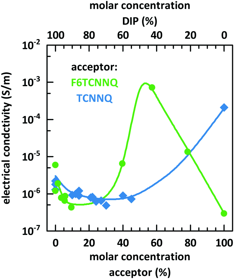 | ||
| Fig. 10 Electrical conductivity determined at room temperature for single component and co-deposited D:A films of DIP, TCNNQ and F6TCNNQ as function of the molar concentration measured. The solid lines are given to guide the eyes. | ||
Measurements on activation energy and electrical conductivity were performed for single-component films of DBTTF, DIP and F6CTNNQ. Furthermore, co-deposited films of various molar ratios were characterised as DBTTF:TCNNQ, DBTTF:F6TCNNQ and DIP:F6TCNNQ. The data for film compositions, electrical conductivities at room temperature and activation energies are collected in ESI† (Table S2). The dependence of electric conductivity and activation energy at room temperature will be discussed in a later part.
Additional systems
More systems were characterised for this study to support findings on the EDA complexes formed by DBTTF and DIP as donor as well as by TCNNQ and F6TCNNQ as acceptor. The respective redox potentials of 6T (Uox = +0.44 V) and F4TCNQ (Ured = +0.13 V) were detected in the same way as for the other materials described here.15Sequential deposition (see ESI†) of F4TCNQ on DBTTF and DIP films was used to produce respective EDA complexes. The absorption spectra are given in Fig. S6 (ESI†). The CT absorption features arise at 1.26 eV for DBTTF:F4TCNQ and 0.98 eV for DIP:F4TCNQ. One has to mention that the absorption spectrum of the here shown DBTTF:F4TCNQ film is different from single crystal spectrum.67 This indicates a different molecular arrangement in the here characterised films as dimerized segregated stacks in the single crystals. The CT absorption energy of EDA complex formed between 6T and F6TCNNQ was determined to be 0.61 eV.35 All redox potential differences and the energies of the CT transition for these EDA complexes are summarised in Table 1 (numbers 6–8).
The formation of EDA complexes upon sequential deposition of F4CTNQ onto single-components films of DBTTF and DIP was confirmed also by X-ray reflectivity measurements (see Fig. S7, ESI†). A new Bragg peak related to a different crystal structure than that of the donor was identified as feature of the formed mixed crystals. Details on the structure and the presence of mixed crystals in co-deposited films of 6T:F6TCNNQ can be found in ref. 35.
Measurements on activation energy and electrical conductivity were performed for co-deposited films of 6T and F6TCNNQ as well as for sequential deposited F4TCNQ on the single-component DBTTF and DIP films. Also, these data for film compositions, electrical conductivities at room temperature and activation energies are collected in ESI† (Table S2).
Discussion
Comprehensive comparison of EDA complexes
We start the discussion with comparison of EDA complexes in terms of optical, structural and vibrational properties. Therefore, the dependence of the CT absorption energy on the redox potential difference is displayed in Fig. 11 for all investigated material pairs. The CT absorption energy has a minimum hνmin at a redox potential difference around 0.4 eV and is increasing for more positive as well as for more negative values of it. The EDA complexes on the more positive side of the redox potential are called neutral, whereas the complexes at the more negative side are named ionic. The redox potential difference with smallest CT absorption energy corresponds to the neutral-ionic boundary En–i–b. Energies of electrostatic interaction, van der Waals interaction and resonance energy due to π-orbital overlap between the involved molecules cause this shift of the minimum CT absorption energy from zero redox potential difference.3,4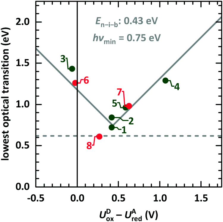 | ||
| Fig. 11 Lowest optical transition of EDA complexes as function of the intermolecular redox potential difference UDox − UAred. The identifiers are taken from Table 1 (green: systems presented here, red: systems from ESI,† and from ref. 9). The solid grey line is fitted following eqn (1).68 The horizontal line gives the typical lower boundary for optical transitions in EDA complexes from literature at 5000 cm−1 (0.62 eV).69,70 | ||
This behaviour is fitted using a simplified description based on the model introduced by Torrance et al.68 using the equation
| hνCPX = |EDHOMO − EALUMO − En–i–b| + hνmin. | (1) |
The study presented here shows a crossing of the neutral-ionic boundary by chemical variation of donor and acceptor molecules. Furthermore, crossing this boundary is possible by chemical substitution77,78 as well as pressure or temperature changes.65,68 Chemical substitution is present for TCNNQ and F6TCNNQ molecules. Even if DBTTF:TCNNQ complexes are appearing close to the neutral-ionic boundary, the DBTTF:F6TCNNQ complex is clearly of ionic nature, and a crossing of the neutral-ionic boundary is present. A temperature-dependent crossing of the neutral-ionic boundary can be ruled out for the DIP containing complexes from absorption measurements shown in Fig. 4. Also, the results of temperature-dependent conductivity measurements to determine the activation energy exclude temperature-induced neutral-ionic transition for all analysed systems.
Now, we compare the morphological and structural properties for the co-deposited films reported here. The van der Waals sizes of the molecules as measure for the molecular sizes are given in Fig. 12, determined from the atomic distances in crystal structures (TCNNQ,79 F6TCNNQ,41,47 DBTTF,45 DIP80) and adding van der Waals radii81 of the respective, terminal atoms. The numbers given for the donor materials DBTTF and DIP are taken from single crystal structures.45,80 The molecular sizes for DIP in the high temperature bulk phase80 give roughly the same unit cell parameters as the thin film phase.82,83 The molecular sizes for the acceptors are taken from mixed crystals reported in literature50,79 and compared to the single crystal data for F6CTNNQ.41
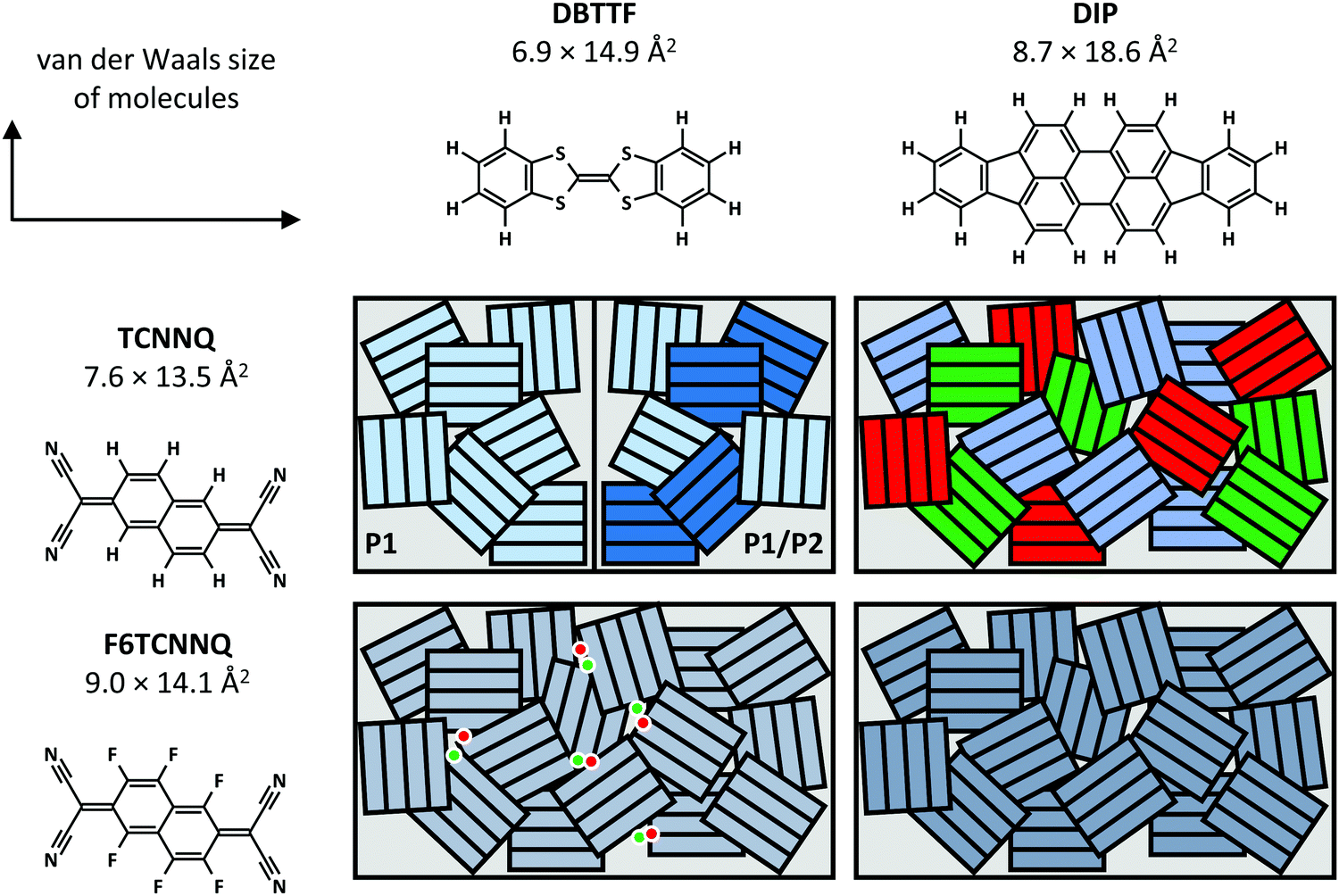 | ||
| Fig. 12 Summary of mixing behaviour for the co-deposited D:A films. The van der Waals sizes of the molecules are determined from the atomic distances in crystal structures (TCNNQ,79 F6TCNNQ,41,47 DBTTF,45 DIP80) and adding van der Waals radii81 of the respective, terminal atoms. Differently coloured rectangles in the schematics indicate different phases: green and red – D and A, shades of blue – different EDA complexes or mixed crystals. The dots show isolated D cations and A anions. | ||
Whereas DBTTF and the acceptors have quite similar sizes, DIP is larger along the long axis of the molecule. Kitaigorodsky identified isoelectronicity and isostructurality as prerequisite to form mixed crystals.5 This means that molecules with similar chemical and crystal structures should be able to form mixed crystals. Similar size of the π-system increases the interaction of the different molecules.49,84–86 Also, dipolar and van der Waals interactions play a key role.14,87 The similar sizes of DBTTF and the acceptors together with the energy level offset results in mixed crystal formation. Mixed crystals are mainly present in equimolar films, where single-component phases are absent. The difference in molecular sizes allows the mixed crystal formation only for a small portion of molecules in DIP:TCNNQ co-deposited films. Clearly phase separation between donor, acceptor and mixed crystals is observed. In contrast, an increased amount of formed mixed crystals is present in co-deposited films of DIP and F6TCNNQ. Seemingly, the energy level offset and the related stronger degree of charge transfer (see next section) are favourable for mixed crystal formation and thermodynamic stabilisation. The overall degree of structural order is higher for DBTTF:TCNNQ than for DBTTF:F6TCNNQ co-deposited films. This might be related to the more comparable short axis of DBTTF and TCNNQ molecules. In contrast, DIP-containing co-deposited films show a higher degree of structural order for F6CTNNQ as acceptor than for TCNNQ due to the mentioned tendency of DIP and TCNNQ to phase-separate. In this case the dipolar and van der Waals interactions on the one side, and the smaller energy level offset on the other side seem to favour the formation of mixed crystals between DIP and F6TCNNQ. In non-equimolar films, phase separation between mixed crystals and the excess single-component crystals is observed.
As mentioned before, the difference in free energy for the formation of distinct mixed crystal polymorphs might be very low. In our case, two polymorphs of DBTTF:TCNNQ mixed crystals are observed. Different π-stacking motifs can be the reason for such behaviour, although the molecules are parallel aligned. However, the orientation of the molecules with respect to the stacking direction might be different as reported for the polymorphs of DBTTF:TCNQ.9 Two different types of charge transfer are concluded for DBTTF:F6TCNNQ co-deposited films. The mixed crystal as EDA complex is observed together with ICT.32 Even if ICT is also reported in mixed crystal films of DBTTF and molybdenum tris[1,2-bis-(trifluoromethyl)ethane-1,2-dithiolene],33 due to the structural dissimilarity of D and A, no structural features related to a second mixed crystal structure are observed there. Therefore, the ICT is attributed to disordered areas close to grain boundaries.32
The EDA complex DBTTF:TCNNQ (P2) appears with negligible degree of CT, whereas the complex DBTTF:TCNNQ (P1) and DBTTF:F6TCNNQ show a charge transfer of about ≈0.26 and ≈0.60 of an electron. The EDA complexes DIP:TCNNQ and DIP:F6TCNNQ show in infra-red transmission and Raman measurements negligible CT. In contrast, infra-red spectroscopy with high angle of incidence reveal a degree of CT of 0.57 for DIP:TCNNQ and 0.84 for DIP:F6TCNNQ.34 The difference between normal and grazing incidence measurements might result in different selection rules and shows a strong anisotropy in these systems. An anisotropy of optical properties was shown before for DIP:F6TCNNQ films by angle-dependent spectroscopic ellipsometry.35 The main feature of EDA complexes is the presence of a charge transfer absorption with an energy lower than the absorption energies of the single-component materials. This criterion is fulfilled for all EDA complexes mentioned in Table 3, regardless of the detected degree of CT. One has to keep in mind that the degree of CT is determined by several factors like energy level offset EDHOMO − EALUMO as well as the specific geometry and the related π-orbital overlap. The latter point is shown by the polymorphism in DBTTF:TCNNQ complexes, where different EDA complex polymorphs show different degrees of CT. Furthermore, even if DIP has for both acceptors the larger energy level offset than DBTTF, the degree of CT is higher for the DIP containing complexes than for the DBTTF complexes with the same acceptor. This might be related to the detailed orbital distribution of the involved D and A molecules. Here the description has to go beyond a dependence on the energy level offset only, similar to the observation for different polymorphs for the same material combination.
Doping via EDA complexes
The basic activation process upon complex doping is still in debate. Different energy barriers are present for thermal activation of the electron from HOMO to LUMO inside the complex or from HOMO of OSC to LUMO of the complex. Measurements of the temperature dependent conductivity of cod-deposited DBTTF:TCNNQ and DBTTF:F6TCNNQ films were unable to solve this point before.32 The measured activation energies were much lower than both activation energy barriers. The influence of complex doping on the conductivity was described as negligible as the single-component DBTTF film and the co-deposited DBTTF:TCNNQ film (10% TCNNQ) showed the similar conductivities and activation energies. The strongly increased conductivity and the reduced activation energy for co-deposited films of DBTTF:F6TCNNQ films in comparison to the single-component DBTTF film was attributed to the presence of ICT doping.To characterise the underlying activation behaviour upon complex doping, the dependence of the electrical conductivity on the activation energy at room temperature is displayed in Fig. 13. The conductivity was analysed by transfer-length method to reduce influence of contact resistance.88 The points with activation energies above 600 meV refer to the single-component films of DBTTF, DIP, F6TCNNQ and 6T together with the co-deposited film of 10% F6TCNNQ and DIP. The data points with an activation energy below 500 meV can be described by a thermally activated behaviour following the equation
 | (2) |
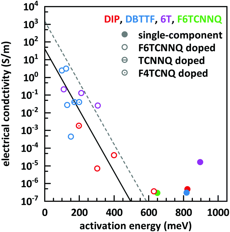 | ||
| Fig. 13 Electrical conductivity vs. activation energy for films of various D:A systems as well as for single-component films. The lines are calculated from eqn (2) with different prefactors (dashed line: 1500 S m−1, solid line: 42 S m−1). The values of the data points shown here are given in the ESI† (see Table S2). | ||
In the region of low dopant concentrations and low conductivities, the observed behaviour was attributed to the thermal activation of ion pairs formed via ICT to generate free charge carriers in doped organic semiconductors.89 The resulting prefactor for ICT doping varies for different material combinations mostly between 102 and 104 S m−1. We conclude therefore that the limiting parameter for the resulting conductivity of EDA complex doping is the same as for ICT doping at low concentrations, namely the generation of free charge carriers from generated ion pairs.
Importantly, the thermally activated behaviour of electrical conductivity shows a smooth transition between complex and ICT doping. One has to keep in mind that ICT might be present for DBTTF:F6TCNNQ films as well. From the frontier orbital positions of the molecules, a similar behaviour for DBTTF:F4TCNQ films is possible. This might be prevented by the applied sequential deposition and a different crystal packing giving also different CT absorption energies (see Table 1). However, limitations of the model can be seen for the class of F6TCNNQ doped DBTTF films. The slope is much higher than for the introduced linear model. A more detailed study would be necessary for a conclusive picture on the material dependence of the model in eqn (2). Furthermore, the system in our study with the lowest CT absorption energy, which is 6T:F6TCNNQ, shows also the highest conductivity for pure complex doping and part of the data points are located at the curve with the prefactor of 1500 S m−1. This can be seen as a hint, that the thermal activation inside the EDA complex is a limiting factor for the generation of charge carriers upon complex doping. Detailed studies on the dependence of the electrical conductivity on the gap of complex dopants might be a challenge for the future.
Conclusion
The present study comprises the characterisation of EDA complexes formed from the donors DBTTF and DIP and the acceptors TCNNQ and F6TCNNQ. EDA complex formation was found for all four D:A combinations. Polymorphism is present for DBTTF:TCNNQ mixed-crystals. The dependence of the CT absorption energy on the redox potential differences of the involved molecules in the EDA complex follows a modulus function [see eqn (1)] considering a minimal CT absorption energy of about 0.62 eV and the energy of the neutral-ionic boundary at a redox potential difference of 0.43 eV which characterises the interaction of the molecules in the mixed crystalline film. Unit cell parameters for the γ-polymorph of DBTTF and the P1 polymorph of DBTTF:TCNNQ were determined from X-ray scattering data. For each donor, the EDA complex containing F6TCNNQ as stronger acceptor shows the higher degree of CT. In contrast, the weaker donor DIP shows for both acceptors the higher degree of CT as the donor DBTTF. A strong anisotropy of vibrational properties was detected for the DIP containing mixed crystalline films. The addition of acceptor to DBTTF films increases the electrical conductivity for low acceptor concentrations. In contrast, the electrical conductivity of co-deposited DIP:acceptor films is reduced for low acceptor concentrations. A peaking conductivity in films was found for an equimolar ratio of DIP and F6TCNNQ which exceeds also the conductivity of the single component films. Thereby, a clear correlation between film morphology, phase-behaviour and conductivity was established for DA systems. The electrical conductivity of films upon complex doping shows the same thermally activated behaviour as for ICT doping.The unified description of the dependence of CT absorption energy on the intermolecular energy level difference is challenging if the related energy levels are unknown. Therefore, only a simplified description is used here,68 using the redox potential difference of D and A molecules and agreeing well with the presented data. This is in line with reports on several other EDA complexes in literature.69,70 Detailed computational calculations12,75,76 often lack on computational time, accurate description and unknown crystal structures. However, the application of the here presented EDA complexes as infra-red absorber seems to be limited to energies above 0.61 eV (≈2000 nm).35,70,90 Also here, the relation between CT absorption energy and redox potential difference given by Torrance et al.68 [see eqn (1)] is applicable.
Anisotropic properties are common for molecular crystals.91–93 This is also pronounced in EDA complex materials due to the presence of two different molecules. The transition dipole moment of the CT absorption is oriented perpendicular to the π-orbital planes of the molecules in the complex.35,94 Absorption and emission features related to D:A interaction are only present if π-stacking is possible, e.g. in co-deposited films, and absent in head-to-tail configurations.95,96 Here we report on anisotropy of vibrational features. The complex-related infra-red modes are present only by applying grazing incidence for the light and are absent in infra-red and Raman measurements with normal incidence/detection directions.
Doping plays a role to improve device performance with increasing charge carrier density, but also disturbing the single-component film morphology.97 This holds also for complex doping. Disorder might help to improve the separation of bound charge pairs in doped films,66,98 it might also help to avoid complex formation and therefore, increase the doping efficiency. Even if doping by EDA complexes is less efficient than electron30,66 or hydrogen31,99 transfer doping, the relation between electrical conductivity and activation energy seems to be universal. Doping has to work for improving hole and electron transport. This is shown for doping by EDA complexes, too. Considering acceptors like TCNNQ and F6TCNNQ as semiconductor, the adding of the donor DBTTF or DIP increases the electrical conductivity. Here also a drastic improvement of the film morphology in co-deposited films related to the charge carrier transport abilities is observed in comparison to the single-component acceptor films.
Author contributions
A. O., A. H., F. S. and W. B. initiated the study and supervised the work. T. M. and P. B. prepared films by vacuum sublimation and performed the analysis by absorption, morphological and room temperature electrical measurements. M. G., H. K. and E. M. prepared films by vacuum sublimation and sequential deposition. They analysed these films by temperature-dependent electrical, X-ray reflectivity, morphological and absorption measurements. G. D., V. B., L. P. and A. H. prepared films and collected morphological and X-ray scattering data at the synchrotrons on self-prepared and films prepared by others. G. D. performed unit cell parameter fitting. G. D. and P. B. performed infra-red measurements. C. K., J. P. and V. B. conducted Raman measurements. A. O. prepared the manuscript draft and all authors contributed to finalize the manuscript.Conflicts of interest
The authors declare no competing financial interest.Acknowledgements
The work was supported financially by Deutsche Forschungsgemeinschaft (DFG – OP159/2-2, SCHR700/20-2, Br 1728/14-2, project no. 239543752). We are grateful for beamtime at The European Synchrotron Radiation Facility (ESRF, beamlines ID10 + ID03) and at the Swiss Light Source (SLS, beamline X04SA). G. D. gratefully acknowledges support from the Carl-Zeiss-Stiftung. W. B. and J. P. acknowledge support by the Bavarian State Ministry for Science and the Arts within the collaborative research network “Solar Technologies go Hybrid” (SolTech). Georg Heimel performed DFT calculations and Jan Hagenlocher helped during synchrotron measurements.References
- H. A. Benesi and J. H. Hildebrand, A Spectrophotometric Investigation of the Interaction of Iodine with Aromatic Hydrocarbons, J. Am. Chem. Soc., 1949, 71, 2703–2707, DOI:10.1021/ja01176a030.
- G. Briegleb and J. Czekalla, Elektronenüberführung durch Lichtabsorption und -emission in Elektronen-Donator-Acceptor-Komplexen, Angew. Chem., 1960, 72, 401–413, DOI:10.1002/ange.19600721203.
- G. Briegleb, Elektronen–Donator–Acceptor–Komplexe, Springer Berlin Heidelberg, Berlin, Heidelberg, 1961 DOI:10.1007/978-3-642-86555-8.
- R. S. Mulliken and W. B. Person, Donor–Acceptor Complexes, Annu. Rev. Phys. Chem., 1962, 13, 107–126, DOI:10.1146/annurev.pc.13.100162.000543.
- A. I. Kitaigorodsky, Mixed Crystals, Springer, Berlin, Heidelberg, 1984. DOI:10.1007/978-3-642-81672-7.
- M. Schwoerer and H. C. Wolf, Organic Crystals of High Conductivity, in Org. Mol. Solids, ed. M. Schwoerer and H. C. Wolf, Wiley-VCH Verlag GmbH, Weinheim, Germany, 2007, pp. 307–349. DOI:10.1002/9783527618651.ch9.
- K. P. Goetz, D. Vermeulen, M. E. Payne, C. Kloc, L. E. McNeil and O. D. Jurchescu, Charge-transfer complexes: New perspectives on an old class of compounds, J. Mater. Chem. C, 2014, 2, 3065–3076, 10.1039/c3tc32062f.
- T. Mori, Charge-Transfer Complexes, in Electronic Properties of Organic Conductors, ed. T. Mori, Springer Japan, Tokyo, 2016, pp. 253–310. DOI:10.1007/978-4-431-55264-2_7.
- K. P. Goetz, J. J. Tsutsumi, S. Pookpanratana, J. Chen, N. S. Corbin, R. K. Behera, V. Coropceanu, C. A. Richter, C. A. Hacker, T. Hasegawa and O. D. Jurchescu, Polymorphism in the 1:1 Charge-Transfer Complex DBTTF–TCNQ and Its Effects on Optical and Electronic Properties, Adv. Electron. Mater., 2016, 2, 1600203, DOI:10.1002/aelm.201600203.
- J. Henderson, M. Masino, L. E. Hatcher, G. Kociok-Köhn, T. Salzillo, A. Brillante, P. R. Raithby, A. Girlando and E. Da Como, New Polymorphs of Perylene:Tetracyanoquinodimethane Charge Transfer Cocrystals, Cryst. Growth Des., 2018, 18, 2003–2009, DOI:10.1021/acs.cgd.7b01391.
- J. Jin, S. Wu, Y. Ma, C. Dong, W. Wang, X. Liu, H. Xu, G. Long, M. Zhang, J. Zhang and W. Huang, Nucleation Control-Triggering Cocrystal Polymorphism of Charge-Transfer Complexes Differing in Physical and Electronic Properties, ACS Appl. Mater. Interfaces, 2020, 12, 19718–19726, DOI:10.1021/acsami.9b23590.
- L. Zhu, E.-G. Kim, Y. Yi and J.-L. Brédas, Charge Transfer in Molecular Complexes with 2,3,5,6-Tetrafluoro-7,7,8,8-tetracyanoquinodimethane (F4-TCNQ): A Density Functional Theory Study, Chem. Mater., 2011, 23, 5149–5159, DOI:10.1021/cm201798x.
- J. Li, G. D’Avino, A. Pershin, D. Jacquemin, I. Duchemin, D. Beljonne and X. Blase, Correlated electron-hole mechanism for molecular doping in organic semiconductors, Phys. Rev. Mater., 2017, 1, 025602, DOI:10.1103/PhysRevMaterials.1.025602.
- I. Salzmann, S. Duhm, G. Heimel, M. Oehzelt, R. Kniprath, R. L. Johnson, J. P. Rabe and N. Koch, Tuning the Ionization Energy of Organic Semiconductor Films: The Role of Intramolecular Polar Bonds, J. Am. Chem. Soc., 2008, 130, 12870–12871, DOI:10.1021/ja804793a.
- B. Wegner, L. Grubert, C. Dennis, A. Opitz, A. Röttger, Y. Zhang, S. Barlow, S. R. Marder, S. Hecht, K. Müllen and N. Koch, Predicting the yield of ion pair formation in molecular electrical doping: redox-potentials versus ionization energy/electron affinity, J. Mater. Chem. C, 2019, 7, 13839–13848, 10.1039/C9TC04500G.
- B. Joo and E.-G. Kim, Controlled electrical doping of organic semiconductors: a combined intra- and intermolecular perspective from first principles, Phys. Chem. Chem. Phys., 2016, 18, 17890–17897, 10.1039/C6CP00827E.
- A. Ciccarese, D. A. Clemente, A. Marzotto and C. Pecile, Polymorphism in the [(TTF)2(TCNE)2] Charge-Transfer Complex, Microsc., Microanal., Microstruct., 1995, 6, 545–550, DOI:10.1051/mmm:1995146.
- T. Salzillo, M. Masino, G. Kociok-Köhn, D. Di Nuzzo, E. Venuti, R. G. Della Valle, D. Vanossi, C. Fontanesi, A. Girlando, A. Brillante and E. Da Como, Structure, Stoichiometry, and Charge Transfer in Cocrystals of Perylene with TCNQ-Fx, Cryst. Growth Des., 2016, 16, 3028–3036, DOI:10.1021/acs.cgd.5b01663.
- L. Zhu, Y. Yi, Y. Li, E.-G. Kim, V. Coropceanu and J.-L. Brédas, Prediction of Remarkable Ambipolar Charge-Transport Characteristics in Organic Mixed-Stack Charge-Transfer Crystals, J. Am. Chem. Soc., 2012, 134, 2340–2347, DOI:10.1021/ja210284s.
- J. Zhang, W. Xu, P. Sheng, G. Zhao and D. Zhu, Organic Donor–Acceptor Complexes as Novel Organic Semiconductors, Acc. Chem. Res., 2017, 50, 1654–1662, DOI:10.1021/acs.accounts.7b00124.
- H.-D. Wu, F.-X. Wang, Y. Xiao and G.-B. Pan, Preparation and ambipolar transistor characteristics of co-crystal microrods of dibenzotetrathiafulvalene and tetracyanoquinodimethane, J. Mater. Chem. C, 2013, 1, 2286–2289, 10.1039/c3tc30112e.
- J. Tsutsumi, T. Yamada, H. Matsui, S. Haas and T. Hasegawa, Competition between Charge-Transfer Exciton Dissociation and Direct Photocarrier Generation in Molecular Donor-Acceptor Compounds, Phys. Rev. Lett., 2010, 105, 226601, DOI:10.1103/PhysRevLett.105.226601.
- Y. Wang, W. Zhu, W. Du, X. Liu, X. Zhang, H. Dong and W. Hu, Cocrystals Strategy towards Materials for Near-Infrared Photothermal Conversion and Imaging, Angew. Chem., Int. Ed., 2018, 57, 3963–3967, DOI:10.1002/anie.201712949.
- W. Chen, S. Sun, G. Huang, S. Ni, L. Xu, L. Dang, D. L. Phillips and M.-D. Li, Unprecedented Improvement of Near-Infrared Photothermal Conversion Efficiency to 87.2% by Ultrafast Non-radiative Decay of Excited States of Self-Assembly Cocrystal, J. Phys. Chem. Lett., 2021, 5796–5801, DOI:10.1021/acs.jpclett.1c01021.
- K. Vandewal, S. Albrecht, E. T. Hoke, K. R. Graham, J. Widmer, J. D. Douglas, M. Schubert, W. R. Mateker, J. T. Bloking, G. F. Burkhard, A. Sellinger, J. M. J. Fréchet, A. Amassian, M. K. Riede, M. D. Mcgehee, D. Neher and A. Salleo, charge-transfer states at organic interfaces, Nat. Mater., 2013, 13, 63–68, DOI:10.1038/nmat3807.
- B. Siegmund, A. Mischok, J. Benduhn, O. Zeika, S. Ullbrich, F. Nehm, M. Böhm, D. Spoltore, H. Fröb, C. Körner, K. Leo and K. Vandewal, Organic narrowband near-infrared photodetectors based on intermolecular charge-transfer absorption, Nat. Commun., 2017, 8, 15421, DOI:10.1038/ncomms15421.
- N. Marchal, W. Van Gompel, M. C. Gélvez-Rueda, K. Vandewal, K. Van Hecke, H.-G. Boyen, B. Conings, R. Herckens, S. Maheshwari, L. Lutsen, C. Quarti, F. C. Grozema, D. Vanderzande and D. Beljonne, Lead-Halide Perovskites Meet Donor–Acceptor Charge-Transfer Complexes, Chem. Mater., 2019, 31, 6880–6888, DOI:10.1021/acs.chemmater.9b01289.
- H. Méndez, G. Heimel, A. Opitz, K. Sauer, P. Barkowski, M. Oehzelt, J. Soeda, T. Okamoto, J. Takeya, J. B. Arlin, J. Y. Balandier, Y. Geerts, N. Koch and I. Salzmann, Doping of organic semiconductors: Impact of dopant strength and electronic coupling, Angew. Chem., Int. Ed., 2013, 52, 7751–7755, DOI:10.1002/anie.201302396.
- H. Méndez, G. Heimel, S. Winkler, J. Frisch, A. Opitz, K. Sauer, B. Wegner, M. Oehzelt, C. Röthel, S. Duhm, D. Többens, N. Koch and I. Salzmann, Charge-transfer crystallites as molecular electrical dopants, Nat. Commun., 2015, 6, 8560, DOI:10.1038/ncomms9560.
- I. Salzmann, G. Heimel, M. Oehzelt, S. Winkler and N. Koch, Molecular Electrical Doping of Organic Semiconductors: Fundamental Mechanisms and Emerging Dopant Design Rules, Acc. Chem. Res., 2016, 49, 370–378, DOI:10.1021/acs.accounts.5b00438.
- A. I. Hofmann, R. Kroon and C. Müller, Doping and processing of organic semiconductors for plastic thermoelectrics, Handb. Org. Mater. Electron. Photonic Devices, Elsevier, 2019, pp. 429–449. DOI:10.1016/b978-0-08-102284-9.00013-9.
- P. Beyer, D. Pham, C. Peter, N. Koch, E. Meister, W. Brütting, L. Grubert, S. Hecht, D. Nabok, C. Cocchi, C. Draxl and A. Opitz, State-of-Matter-Dependent Charge-Transfer Interactions between Planar Molecules for Doping Applications, Chem. Mater., 2019, 31, 1237–1249, DOI:10.1021/acs.chemmater.8b01447.
- A. Opitz, C. Peter, B. Wegner, H. S. S. R. Matte, A. Röttger, T. Florian, X. Xu, P. Beyer, L. Grubert, S. Hecht, V. Belova, A. Hinderhofer, F. Schreiber, C. Kasper, J. Pflaum, Y. Zhang, S. Barlow, S. R. Marder and N. Koch, Ordered Donor–Acceptor Complex Formation and Electron Transfer in Co-deposited Films of Structurally Dissimilar Molecules, J. Phys. Chem. C, 2020, 124, 11023–11031, DOI:10.1021/acs.jpcc.0c02465.
- G. Duva, P. Beyer, R. Scholz, V. Belova, A. Opitz, A. Hinderhofer, A. Gerlach and F. Schreiber, Ground-state charge-transfer interactions in donor:acceptor pairs of organic semiconductors – a spectroscopic study of two representative systems, Phys. Chem. Chem. Phys., 2019, 21, 17190–17199, 10.1039/C9CP02939G.
- G. Duva, L. Pithan, C. Zeiser, B. Reisz, J. Dieterle, B. Hofferberth, P. Beyer, L. Bogula, A. Opitz, S. Kowarik, A. Hinderhofer, A. Gerlach and F. Schreiber, Thin-Film Texture and Optical Properties of Donor/Acceptor Complexes. Diindenoperylene/F6TCNNQ vs. Alpha-Sexithiophene/F6TCNNQ, J. Phys. Chem. C, 2018, 122, 18705–18714, DOI:10.1021/acs.jpcc.8b03744.
- G. Duva, Structural and Spectroscopic Studies of Molecular Semiconductor Donor:Acceptor Systems for Organic Optoelectronics, doctoral thesis at Universität Tübingen, 2019 DOI:10.15496/publikation-33364.
- G. M. Day, T. G. Cooper, A. J. Cruz-Cabeza, K. E. Hejczyk, H. L. Ammon, S. X. M. Boerrigter, J. S. Tan, R. G. Della Valle, E. Venuti, J. Jose, S. R. Gadre, G. R. Desiraju, T. S. Thakur, B. P. van Eijck, J. C. Facelli, V. E. Bazterra, M. B. Ferraro, D. W. M. Hofmann, M. A. Neumann, F. J. J. Leusen, J. Kendrick, S. L. Price, A. J. Misquitta, P. G. Karamertzanis, G. W. A. Welch, H. A. Scheraga, Y. A. Arnautova, M. U. Schmidt, J. van de Streek, A. K. Wolf and B. Schweizer, Significant progress in predicting the crystal structures of small organic molecules – a report on the fourth blind test, Acta Crystallogr., Sect. B: Struct. Sci., 2009, 65, 107–125, DOI:10.1107/S0108768109004066.
- J. Yang, S. De, J. E. Campbell, S. Li, M. Ceriotti and G. M. Day, Large-Scale Computational Screening of Molecular Organic Semiconductors Using Crystal Structure Prediction, Chem. Mater., 2018, 30, 4361–4371, DOI:10.1021/acs.chemmater.8b01621.
- T. Kakudate, N. Yoshimoto and Y. Saito, Polymorphism in pentacene thin films on SiO2 substrate, Appl. Phys. Lett., 2007, 90, 081903, DOI:10.1063/1.2709516.
- A. Brillante, I. Bilotti, R. G. Della Valle, E. Venuti, S. Milita, C. Dionigi, F. Borgatti, A. N. Lazar, F. Biscarini, M. Mas-Torrent, N. S. Oxtoby, N. Crivillers, J. Veciana, C. Rovira, M. Leufgen, G. Schmidt and L. W. Molenkamp, The four polymorphic modifications of the semiconductor dibenzo-tetrathiafulvalene, CrystEngComm, 2008, 10, 1899–1909, 10.1039/b810993a.
- J. Li, I. Duchemin, O. M. Roscioni, P. Friederich, M. Anderson, E. Da Como, G. Kociok-Köhn, W. Wenzel, C. Zannoni, D. Beljonne, X. Blase and G. D’Avino, Host dependence of the electron affinity of molecular dopants, Mater. Horiz., 2019, 6, 107–114, 10.1039/c8mh00921j.
- M. Nieger, Experimental Crystal Structure Determination, CSD Commun. CCDC 14262 (2015) DOI:10.5517/cc1jw2s8.
- M. Mamada and Y. Yamashita, Triclinic polymorph of dibenzotetrathiafulvalene, Acta Crystallogr., Sect. E: Struct. Rep. Online, 2009, 65, o2083, DOI:10.1107/S1600536809030013.
- H. Kobayashi and J. Nakayama, The Crystal Structure of the Charge-transfer Complex of Dibenzotetrathiafulvalene-Tetracyanoquinodimethane, DBTTF–TCNQ, Bull. Chem. Soc. Jpn., 1981, 54, 2408–2411, DOI:10.1246/bcsj.54.2408.
- T. J. Emge, F. M. Wiygul, J. S. Chappell, A. N. Bloch, J. P. Ferraris, D. O. Cowan and T. J. Kistenmacher, Crystal Structures for the Electron Donor Dibenzotetrathiafulavalene, DBTTF, and Its Mixed-stack Charge-transfer Salts with the Electron Acceptors 7,7,8,8-tetracyano-p-quinodimethane, TCNQ, and 2,5-difluoro-7,7,8,8-tetracyano-p-quinodime, Mol. Cryst. Liq. Cryst., 1982, 87, 137–161, DOI:10.1080/00268948208083778.
- T. J. Emge, W. A. Bryden, F. M. Wiygul, D. O. Cowan, T. J. Kistenmacher and A. N. Bloch, Structure of an organic charge-transfer salt derived from dibenzotetrathiafulvalene and tetrafluorotetracyanoquino-dimethane (DBTTF–TCNQF4). Observation of a high-temperature phase transition, J. Chem. Phys., 1982, 77, 3188–3197, DOI:10.1063/1.444193.
- P. Hu, S. Wang, A. Chaturvedi, F. Wei, X. Zhu, X. Zhang, R. Li, Y. Li, H. Jiang, Y. Long and C. Kloc, Impact of C–H⋯X (X = F, N) and π–π Interactions on Tuning the Degree of Charge Transfer in F6TNAP-Based Organic Binary Compound Single Crystals, Cryst. Growth Des., 2018, 18, 1776–1785, DOI:10.1021/acs.cgd.7b01669.
- D. Nečas and P. Klapetek, Gwyddion: an open-source software for SPM data analysis, Open Phys., 2012, 10, 181–188, DOI:10.2478/s11534-011-0096-2.
- A. Aufderheide, K. Broch, J. Novák, A. Hinderhofer, R. Nervo, A. Gerlach, R. Banerjee and F. Schreiber, Mixing-Induced Anisotropic Correlations in Molecular Crystalline Systems, Phys. Rev. Lett., 2012, 109, 156102, DOI:10.1103/PhysRevLett.109.156102.
- R. R. Dasari, X. Wang, R. A. Wiscons, H. F. Haneef, A. Ashokan, Y. Zhang, M. S. Fonari, S. Barlow, V. Coropceanu, T. V. Timofeeva, O. D. Jurchescu, J. Brédas, A. J. Matzger and S. R. Marder, Charge-Transport Properties of F6TNAP-Based Charge-Transfer Cocrystals, Adv. Funct. Mater., 2019, 29, 1904858, DOI:10.1002/adfm.201904858.
- A. Girlando, Charge sensitive vibrations and electron-molecular vibration coupling in bis(ethylenedithio)-tetrathiafulvalene (BEDT-TTF), J. Phys. Chem. C, 2011, 115, 19371–19378, DOI:10.1021/jp206171r.
- J. S. Chappell, A. N. Bloch, W. A. Bryden, M. Maxfield, T. O. Poehler and D. O. Cowan, Degree of charge transfer in organic conductors by infrared absorption spectroscopy, J. Am. Chem. Soc., 1981, 103, 2442–2443, DOI:10.1021/ja00399a066.
- A. Girlando, A. Painelli and C. Pecile, Electron-Intramolecular Phonon Coupling in regular and Dimerized Mixed Stack Organic Semiconductors, Mol. Cryst. Liq. Cryst., 2007, 120, 17–26, DOI:10.1080/00268948508075754.
- A. Girlando, Comment on Polymorphism in the 1:1 Charge-Transfer Complex DBTT-TCNQ and Its Effects on Optical and Electronic Properties, Adv. Electron. Mater., 2017, 3, 1600437, DOI:10.1002/aelm.201600437.
- A. Girlando, C. Pecile and A. Painelli, Vibrational spectroscopy of mixed stack organic semiconductors: comparison with segregated stack systems, Le J. Phys., Colloq., 1983, 44, C3-1547–C3-1550, DOI:10.1051/jphyscol/1983060.
- M. Tanaka, M. Shimizu, Y. Saito and J. Tanaka, Raman spectra of radical ion DBTTF complexes; relation between Raman frequency and formal charge, Chem. Phys. Lett., 1986, 125, 594–596, DOI:10.1016/0009-2614(86)87106-8.
- C. Ouyang, X. Qian, K. Wang and H. Liu, Controllable one-dimension nanostructures of CuTNAP for field emission properties, Dalton Trans., 2012, 41, 14391–14396, 10.1039/c2dt31897k.
- R. Scholz, L. Gisslén, B.-E. Schuster, M. B. Casu, T. Chassé, U. Heinemeyer and F. Schreiber, Resonant Raman spectra of diindenoperylene thin films, J. Chem. Phys., 2011, 134, 014504, DOI:10.1063/1.3514709.
- D. Shi, Y. Chen, H. Pang, F. Meng, Y. Sun, K. Liu and H. Liu, Synthesis, Crystal Structure, and Spectral Characterization of Novel Three-dimensional Supramolecular Networks with One-dimensional Channels Based on Keggin-type Polyoxoanions and Mixed-Valence Dibenzotetrathiafulvalenes, Zeitschrift Für Naturforsch. B, 2007, 62, 195–199, DOI:10.1515/znb-2007-0208.
- H. L. Cheng, Y. S. Mai, W. Y. Chou, L. R. Chang and X. W. Liang, Thickness-dependent structural evolutions and growth models in relation to carrier transport properties in polycrystalline pentacene thin films, Adv. Funct. Mater., 2007, 17, 3639–3649, DOI:10.1002/adfm.200700207.
- C. Adamo and V. Barone, Toward reliable density functional methods without adjustable parameters: the PBE0 model, J. Chem. Phys., 1999, 110, 6158–6170, DOI:10.1063/1.478522.
- J.-D. Chai and M. Head-Gordon, Long-range corrected hybrid density functionals with damped atom–atom dispersion corrections, Phys. Chem. Chem. Phys., 2008, 10, 6615, 10.1039/b810189b.
- N. Shioya, R. Murdey, K. Nakao, H. Yoshida, T. Koganezawa, K. Eda, T. Shimoaka and T. Hasegawa, Alternative Face-on Thin Film Structure of Pentacene, Sci. Rep., 2019, 9, 1–7, DOI:10.1038/s41598-018-37166-6.
- K. Koynov, A. Bahtiar, T. Ahn, R. M. Cordeiro, H. H. Hörhold and C. Bubeck, Molecular weight dependence of chain orientation and optical constants of thin films of the conjugated polymer MEH-PPV, Macromolecules, 2006, 39, 8692–8698, DOI:10.1021/ma0611164.
- M. Masino, N. Castagnetti and A. Girlando, Phenomenology of the Neutral-Ionic Valence Instability in Mixed Stack Charge-Transfer Crystals, Crystals, 2017, 7, 108, DOI:10.3390/cryst7040108.
- M. L. Tietze, J. Benduhn, P. Pahner, B. Nell, M. Schwarze, H. Kleemann, M. Krammer, K. Zojer, K. Vandewal and K. Leo, Elementary steps in electrical doping of organic semiconductors, Nat. Commun., 2018, 9, 1182, DOI:10.1038/s41467-018-03302-z.
- G. Saito, H. Kumagai, J. Tanaka, T. Enoki and H. Inokuchi, Organic Metals Based on Hexamethylenetetratellurafulvalene (HMTTeF), Mol. Cryst. Liq. Cryst., 1985, 120, 337–340, DOI:10.1080/00268948508075814.
- J. B. Torrance, J. E. Vazquez, J. J. Mayerle and V. Y. Lee, Discovery of a Neutral-to-Ionic Phase Transition in Organic Materials, Phys. Rev. Lett., 1981, 46, 253–257, DOI:10.1103/PhysRevLett.46.253.
- G. Saito and Y. Yoshida, Development of conductive organic molecular assemblies: Organic metals, superconductors, and exotic functional materials, Bull. Chem. Soc. Jpn., 2007, 80, 1–137, DOI:10.1246/bcsj.80.1.
- G. Saito, H. Sasaki, T. Aoki, Y. Yoshida, A. Otsuka, H. Yamochi, O. O. Drozdova, K. Yakushi, H. Kitagawa and T. Mitani, Complex formation of ethylenedioxyethylenedithiotetrathiafulvalene (EDOEDT-TTF: EOET) and its self-assembling ability, J. Mater. Chem., 2002, 12, 1640–1649, 10.1039/b110605h.
- G. Saito, H. Ikegami, Y. Yoshida, O. O. Drozdova, K. Nishimura, S. Horiuchi, H. Yamochi, A. Otsuka, T. Hiramatsu, M. Maesato, T. Nakamura, T. Akutagawa and T. Yumoto, Ionicity Phase Diagram of Trifluoromethyl-TCNQ (CF3TCNQ) Charge-Transfer Solids, Bull. Chem. Soc. Jpn., 2010, 83, 1462–1480, DOI:10.1246/bcsj.20100102.
- J. Ferraris, D. O. Cowan, V. Walatka and J. H. Perlstein, Electron transfer in a new highly conducting donor-acceptor complex, J. Am. Chem. Soc., 1973, 95, 948–949, DOI:10.1021/ja00784a066.
- T. J. Kistenmacher, T. E. Phillips and D. O. Cowan, The crystal structure of the 1:1 radical cation–radical anion salt of 2,2′-bis-l,3-dithiole (TTF) and 7,7,8,8-tetracyanoquinodimethane (TCNQ), Acta Crystallogr., Sect. B: Struct. Crystallogr. Cryst. Chem., 1974, 30, 763–768, DOI:10.1107/s0567740874003669.
- G. Brocks, Theoretical study of the charge transfer in the organic crystal of dimethylquaterthiophene and tetrafluoro-tetracyanoquinodimethane, Phys. Rev. B, 1997, 55, 6816–6819, DOI:10.1103/PhysRevB.55.6816.
- A. M. Valencia and C. Cocchi, Electronic and Optical Properties of Oligothiophene-F4TCNQ Charge-Transfer Complexes: The Role of the Donor Conjugation Length, J. Phys. Chem. C, 2019, 123, 9617–9623, DOI:10.1021/acs.jpcc.9b01390.
- Y. Kato, H. Matsumoto and T. Mori, Absence of HOMO/LUMO Transition in Charge-Transfer Complexes of Thienoacenes, J. Phys. Chem. A, 2021, 125, 146–153, DOI:10.1021/acs.jpca.0c08925.
- N. Castagnetti, M. Masino, C. Rizzoli, A. Girlando and C. Rovira, Mixed stack charge transfer crystals: Crossing the neutral-ionic borderline by chemical substitution, Phys. Rev. Mater., 2018, 2, 024602, DOI:10.1103/PhysRevMaterials.2.024602.
- T. Uekusa, R. Sato, D. Yoo, T. Kawamoto and T. Mori, Transistor Characteristics of Charge-Transfer Complexes Observed across a Neutral-Ionic Transition, ACS Appl. Mater. Interfaces, 2020, 12, 24174–24183, DOI:10.1021/acsami.0c03898.
- J. Toyoda, A. Oda, I. Murata, A. Kawamoto, J. Tanaka and K. Nakasuji, Crystal Structure of an Alternated Stacking Charge-Transfer Complex of 2,7-Bis(methylthio)-1,6-dithiapyrene (MTDTPY) with Tetracyano-2,6-naphthoquinodimethane (TNAP), Bull. Chem. Soc. Jpn., 1993, 66, 2115–2117, DOI:10.1246/bcsj.66.2115.
- M. A. Heinrich, J. Pflaum, A. K. Tripathi, W. Frey, M. L. Steigerwald and T. Siegrist, Enantiotropic Polymorphism in Diindenoperylene, J. Phys. Chem. C, 2007, 111, 18878–18881, DOI:10.1021/jp0748967.
- M. Mantina, A. C. Chamberlin, R. Valero, C. J. Cramer and D. G. Truhlar, Consistent van der Waals Radii for the Whole Main Group, J. Phys. Chem. A, 2009, 113, 5806–5812, DOI:10.1021/jp8111556.
- S. Kowarik, A. Gerlach, S. Sellner, L. Cavalcanti, O. Konovalov and F. Schreiber, Real-time X-ray diffraction measurements of structural dynamics and polymorphism in diindenoperylene growth, Appl. Phys. A, 2009, 95, 233–239, DOI:10.1007/s00339-008-5012-2.
- N. Mrkyvkova, M. Hodas, J. Hagara, P. Nadazdy, Y. Halahovets, M. Bodik, K. Tokar, J. W. Chai, S. J. Wang, D. Z. Chi, A. Chumakov, O. Konovalov, A. Hinderhofer, M. Jergel, E. Majkova, P. Siffalovic and F. Schreiber, Diindenoperylene thin-film structure on MoS2 monolayer, Appl. Phys. Lett., 2019, 114, 251906, DOI:10.1063/1.5100282.
- A. Hinderhofer and F. Schreiber, Organic–Organic Heterostructures: Concepts and Applications, ChemPhysChem, 2012, 13, 628–643, DOI:10.1002/cphc.201100737.
- J.-O. Vogel, I. Salzmann, S. Duhm, M. Oehzelt, J. P. Rabe and N. Koch, Phase-separation and mixing in thin films of co-deposited rod-like conjugated molecules, J. Mater. Chem., 2010, 20, 4055–4066, 10.1039/b927594k.
- R. C. Wheland, Correlation of electrical conductivity in charge-transfer complexes with redox potentials, steric factors, and heavy atom effects, J. Am. Chem. Soc., 1976, 98, 3926–3930, DOI:10.1021/ja00429a031.
- M. Schwarze, W. Tress, B. Beyer, F. Gao, R. Scholz, C. Poelking, K. Ortstein, A. A. Gunther, D. Kasemann, D. Andrienko and K. Leo, Band structure engineering in organic semiconductors, Science, 2016, 352, 1446–1449, DOI:10.1126/science.aaf0590.
- S. Luan and G. W. Neudeck, An experimental study of the source/drain parasitic resistance effects in amorphous silicon thin film transistors, J. Appl. Phys., 1992, 72, 766–772, DOI:10.1063/1.351809.
- M. Schwarze, C. Gaul, R. Scholz, F. Bussolotti, A. Hofacker, K. S. Schellhammer, B. Nell, B. D. Naab, Z. Bao, D. Spoltore, K. Vandewal, J. Widmer, S. Kera, N. Ueno, F. Ortmann and K. Leo, Molecular parameters responsible for thermally activated transport in doped organic semiconductors, Nat. Mater., 2019, 18, 242–248, DOI:10.1038/s41563-018-0277-0.
- G. Saito and T. Murata, Mixed valency in organic charge transfer complexes, Philos. Trans. R. Soc., A, 2008, 366, 139–150, DOI:10.1098/rsta.2007.2146.
- M. I. Alonso, M. Garriga, N. Karl, J. O. Ossó and F. Schreiber, Anisotropic optical properties of single crystalline PTCDA studied by spectroscopic ellipsometry, Org. Electron., 2002, 3, 23–31, DOI:10.1016/S1566-1199(01)00027-1.
- J. O. Ossó, F. Schreiber, V. Kruppa, H. Dosch, M. Garriga, M. I. Alonso and F. Cerdeira, Controlled Molecular Alignment in Phthalocyanine Thin Films on Stepped Sapphire Surfaces, Adv. Funct. Mater., 2002, 12, 455–460, DOI:10.1002/1616-3028(20020618)12:6/7<455::AID-ADFM455>3.0.CO;2-I.
- M. Dressel, B. Gompf, D. Faltermeier, A. K. Tripathi, J. Pflaum and M. Schubert, Kramers-Kronig-consistent optical functions of anisotropic crystals: generalized spectroscopic ellipsometry on pentacene, Opt. Express, 2008, 16, 19770, DOI:10.1364/OE.16.019770.
- V. Belova, P. Beyer, E. Meister, T. Linderl, M.-U. Halbich, M. Gerhard, S. Schmidt, T. Zechel, T. Meisel, A. V. Generalov, A. S. Anselmo, R. Scholz, O. Konovalov, A. Gerlach, M. Koch, A. Hinderhofer, A. Opitz, W. Brütting and F. Schreiber, Evidence for Anisotropic Electronic Coupling of Charge Transfer States in Weakly Interacting Organic Semiconductor Mixtures, J. Am. Chem. Soc., 2017, 139, 8474–8486, DOI:10.1021/jacs.7b01622.
- M. Aghamohammadi, A. Fernández, M. Schmidt, A. Pérez-Rodríguez, A. R. Goñi, J. Fraxedas, G. Sauthier, M. Paradinas, C. Ocal and E. Barrena, Influence of the Relative Molecular Orientation on Interfacial Charge-Transfer Excitons at Donor/Acceptor Nanoscale Heterojunctions, J. Phys. Chem. C, 2014, 118, 14833–14839, DOI:10.1021/jp5041579.
- S. Hammer, C. Zeiser, M. Deutsch, B. Engels, K. Broch and J. Pflaum, Spatial Anisotropy of Charge Transfer at Perfluoropentacene–Pentacene (001) Single-Crystal Interfaces and its Relevance for Thin Film Devices, ACS Appl. Mater. Interfaces, 2020, 12, 53547–53556, DOI:10.1021/acsami.0c17152.
- K. Walzer, B. Maennig, M. Pfeiffer, K. Leo, B. Männig, M. Pfeiffer, K. Leo, B. Maennig, M. Pfeiffer and K. Leo, Highly efficient organic devices based on electrically doped transport layers, Chem. Rev., 2007, 107, 1233–1271, DOI:10.1021/cr050156n.
- A. Mityashin, Y. Olivier, T. Van Regemorter, C. Rolin, S. Verlaak, N. G. Martinelli, D. Beljonne, J. Cornil, J. Genoe and P. Heremans, Unraveling the Mechanism of Molecular Doping in Organic Semiconductors, Adv. Mater., 2012, 24, 1535–1539, DOI:10.1002/adma.201104269.
- B. Lüssem, C.-M. M. Keum, D. Kasemann, B. Naab, Z. Bao and K. Leo, Doped Organic Transistors, Chem. Rev., 2016, 116, 13714–13751, DOI:10.1021/acs.chemrev.6b00329.
Footnotes |
| † Electronic supplementary information (ESI) available. See DOI: 10.1039/d1ma00578b |
| ‡ The term charge-transfer complex is avoided here due to the existence of electron donor–acceptor complexes without notable charge transfer. |
| This journal is © The Royal Society of Chemistry 2022 |