 Open Access Article
 This Open Access Article is licensed under a Creative Commons Attribution-Non Commercial 3.0 Unported Licence
Ultrashort and metastable doping of the ZnO surface by photoexcited defects
Lukas
Gierster
 *ab,
Sesha
Vempati†
b and
Julia
Stähler
ab
*ab,
Sesha
Vempati†
b and
Julia
Stähler
ab
aHumbolt-Universität zu Berlin, Institut für Chemie, Brook-Taylor-Str. 2, 12489 Berlin, Germany. E-mail: lukas.gierster@hu-berlin.de
bFritz-Haber-Institut der Max-Planck-Gesellschaft, Abt. Physikalische Chemie, Faradayweg 4–6, 14195 Berlin, Germany
First published on 21st March 2022
Abstract
Shallow donors in semiconductors are known to form impurity bands that induce metallic conduction at sufficient doping densities. The perhaps most direct analogy to such doping in optically excited semiconductors is the photoexcitation of deep electronic defects or dopant levels, creating defect excitons (DX) which may act like shallow donors. In this work, we use time- and angle-resolved photoelectron spectroscopy to observe and characterize DX at the surface of ZnO. The DX are created on a femtosecond timescale upon photoexcitation and have a spatial extent of few nanometers that is confined to the ZnO surface. The localized electronic levels lie at 150 meV below the Fermi energy, very similar to the shallow donor states induced by hydrogen doping [Deinert et al., Phys. Rev. B: Condens. Matter Mater. Phys., 2015, 91, 235313]. The transient dopants exhibit a multi-step decay ranging from hundreds of picoseconds to 77 μs and even longer. By enhancing the DX density, a Mott transition occurs, enabling the ultrafast metallization of the ZnO surface, which we have described previously [Gierster et al., Nat. Commun., 2021, 12, 978]. Depending on the defect density, the duration of the photoinduced metallization ranges from picoseconds to μs and longer, corresponding to the decay dynamics of the DX. The metastable lifetime of the DX is consistent with the observation of persistent photoconductivity (PPC) in ZnO reported in the literature [Madel et al., J. Appl. Phys., 2017, 121, 124301]. In agreement with the theory on PPC [Lany and Zunger, Phys. Rev. B: Condens. Matter Mater. Phys., 2005, 72, 035215], the deep defects are attributed to oxygen vacancies due to their energetic position in the band gap and their formation by surface photolysis upon UV illumination. We show that the photoexcitation of these defects is analogous to chemical doping and enables the transient control of material properties, such as the electrical conductivity, from ultrafast to metastable timescales. The same mechanism should be at play in other semiconductor compounds with deep defects.
1 Introduction
Chemical doping of solids can lead to drastic changes in their conduction, optical and magnetic properties.1 Photoexcitation can induce similar phenomena even on ultrafast timescales, coining the term “photodoping”.2–4 However, photodoping often denotes optical excitation across the band gap of the material,2,5,6 creating holes in the valence band (VB) and electrons in the conduction band (CB). Such photoexcitation can lead to changes analogous to chemical doping in particular materials, such as Mott insulators.5,7 In conventional semiconductors and arguably in most materials, however, no true doping effect should occur as photoexcitation generates both charge carrier types – electrons and holes – simultaneously. This is different to chemical doping, which adds either additional electrons to the CB (n-type doping) or additional holes to the VB (p-type doping) from impurity levels. The achievement of a qualitatively similar effect in photoexcited semiconductors requires the exploration of alternative pathways, for example, the photoexcitation across heterolayers which separates the charges.8 Alternatively, electrons can directly be excited from occupied deep defects, which creates a localized hole and a comparably delocalized electron. Such defect excitons (DX) are the supposed origin of the persistent photoconductivity (PPC) (i.e. conductivity that persists for long times, up to days after photoexcitation) observed in many semiconductors.9 As discussed below, they represent the perhaps most direct analogy to chemical doping.Fig. 1 illustrates the similarity of a photoexcited deep defect and chemical doping. Electron doping in semiconductors is described by so-called shallow donors.10 An impurity atom (or lattice defect) with a different valency is introduced into the host. While the system stays charge neutral, an electron can be released from the impurity into the CB, leaving behind a positively charged hole. This happens spontaneously and leads to the formation of a hydrogen-like state (extending over several lattice sites) from where electrons can become free carriers by thermal activation with Eact ≈ kBT, see Fig. 1a. Hence, shallow donors in a low concentration lead to thermally activated conductivity in the semiconductor. Yet, at a sufficient density, the Mott transition occurs, at which electrons delocalize and form a metallic band (impurity band),1 allowing conduction down to zero K, cf.Fig. 1b. If photoexcitation is to have the same effect as n-type chemical doping in semiconductors, it would not only lead to additional electrons in the CB, but in addition these electrons should be first localized and then form a metallic band at a critical density of photodoping. A species that could in principle feature the exact same behaviour as shallow donors is photoexcited deep donors, i.e. in-gap states induced by impurities or defects that are too far from the CB edge for thermal activation, cf.Fig. 1c. Here, the electron is much more localized at the impurity as compared to the shallow donor, more like a particle in a box than a hydrogen-like state.10 However, an external stimulus such as optical excitation can produce a DX, i.e. a bound electron in the hydrogenic potential of a photoionized impurity. This state is very similar to the shallow donor (cf.Fig. 1a and c), as has been pointed out by recent conceptual and theoretical work.11,12 The question is if this would also lead to a doping effect, i.e. photoinduced (thermally activated) conductivity and, eventually, the Mott semiconductor-to-metal transition, in the sense of an exciton Mott transition of DX.
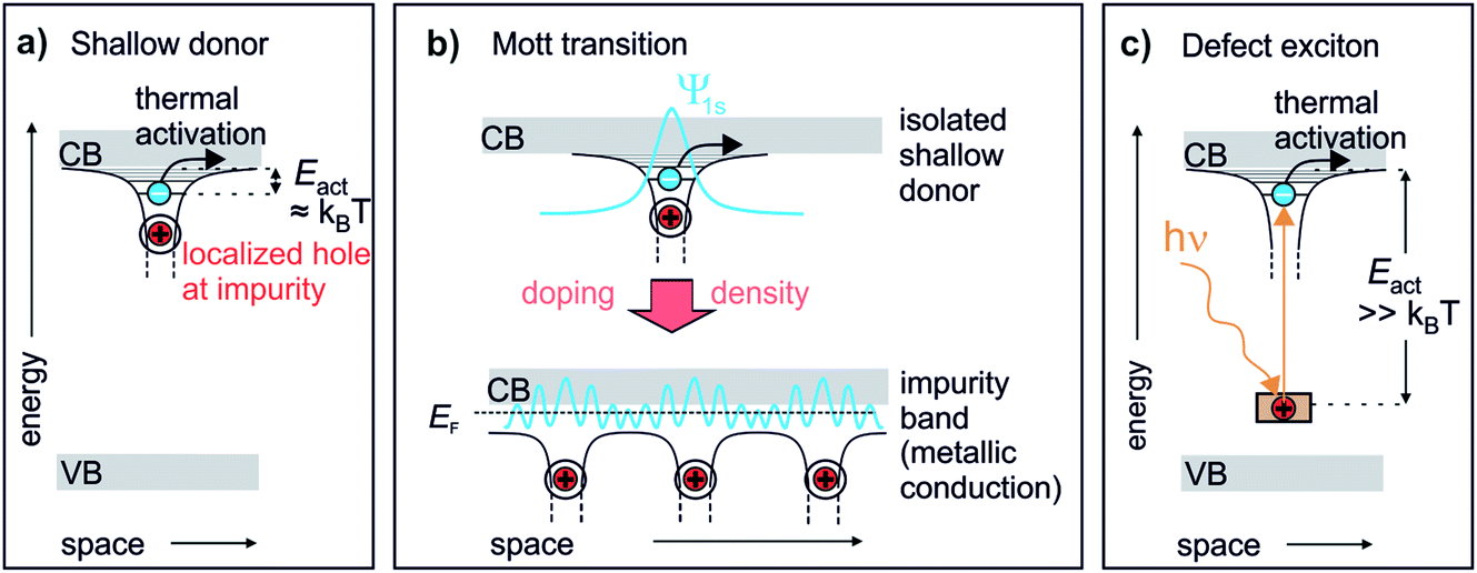 | ||
| Fig. 1 The defect exciton as a bridging concept between shallow and photoexcited deep donors in a semiconductor. (a) Textbook view of a shallow donor: an impurity or defect with a different valency to that of the host releases an electron into the ZnO CB. The electron is bound in a hydrogenic potential to the positively charged impurity and can be freed by thermal activation with kBT. (b) Mott transition: shallow donors at low densities lead to thermally activated conduction. At a critical density, a semiconductor-to-metal transition occurs. The electrons delocalize and form a metallic band (impurity band).1 (c) Deep donors lead to an occupied state within the band gap too far away from the CB for thermal activation. Upon optical excitation, a bound state in the hydrogenic potential of the hole is formed, similar to the shallow donor. | ||
Turning from concepts to real systems, pioneering work by Katsumoto et al.13 showed that the photoexcitation of deep defects can be used to influence the doping density in a GaAs compound, up to reaching a Mott semiconductor-to-metal transition. The system was chemically doped close to the Mott transition and photoexcitation was used to fine-tune the doping density across the Mott density. This is an important step to demonstrate photodoping by DX. However, it remains an open question if nominally undoped semiconductors can also be photodoped by DX up to metallization. Moreover, Katsumoto et al.13 inferred from transport measurements that photoexcited deep defects lead to the Mott transition. The DX themselves, i.e. localized electrons bound to holes, and eventually their evolution into an impurity band is impossible to resolve in such an experiment.
DX most likely also play an important role in the conductive properties of ZnO, a wide-band gap (Egap = 3.4 eV) semiconductor, which has been heavily studied due to its potential for optoelectronic applications and photocatalysis. In ZnO, PPC is observed with lifetimes ranging from below seconds to hours and longer,14–16 and the effect has been attributed theoretically to photoexcited oxygen vacancies which form deep defect levels.17–19 In fact, photoexcitation could be the long searched for bridge between the notorious (unintentional) n-type doping and oxygen vacancies in ZnO.18 A metastable doping effect results from the charged defect distorting the lattice locally, forming a polaronic state, which creates an energetic barrier that has to be overcome by thermal excitation prior to electron–hole recombination.17,18 The theory is supported by experimental findings such as the sensitivity to oxygen exposure14 and the ability to create PPC with photon energies below the band gap.14,20 Furthermore, the rise of the conductivity typically never saturates after switching on the illumination, which is attributed to the photogeneration of oxygen vacancies at the ZnO surface,14,15 an interpretation supported by X-ray photoelectron spectroscopy that evidenced the formation of a Zn-rich surface.21 It is still being discussed, though, whether photoexcited oxygen vacancies are responsible for both short- and long-lived PPC, or if the photodesorption of adsorbed oxygen as an alternative mechanism is at play.16 Moreover, even though deep defects such as oxygen vacancies are widely accepted as source of PPC, the mechanism is usually discussed by assuming that ZnO exhibits upward surface band bending in equilibrium, i.e. an electron depletion layer with low conductivity.15,16,22,23 In this picture, upon photoexcitation of deep defects or across the band gap, electrons are driven into the subsurface, while holes accumulate at the surface. This may contribute in two ways to PPC. Firstly, photoexcited electrons in the subsurface may lead to conductivity for rather long times, as the recombination is slowed by the energy barrier resulting from the band bending.16,22,23 Secondly, the electron–hole separation counteracts the equilibrium band bending (a surface photovoltage effect), eventually leading to flat bands, thereby increasing the surface conductivity with respect to the equilibrium.23 The question is, though, whether upward band bending is at all required (and an adequate assumption) to explain the PPC effect. DX themselves are already predicted to have long lifetimes. Moreover, if DX are formed at the surface, then the surface electronic structure of ZnO would rather be characterized by downward band bending instead of upward band bending or flat bands. This is well known from doping with shallow donors at semiconductor surfaces, for example due to H “doping” by adsorption at ZnO.24 Ultimately, at sufficient DX densities, the surface would become metallic.
In our previous work, we showed that, by photoexciting deep defects at its surface, ZnO indeed shows signatures of transient surface doping.25 The surface is metallized within femtoseconds and returns to the semiconducting state within a sub-ns timescale. Upon tuning through the phase transition by a variation of the laser fluence, the effective mass follows the critical behaviour of Mott semiconductor-to-metal transitions, and we observe transient downward band bending concomitant with metallization, all consistent with photodoping by shallow donor-like DX. In this paper, we extend this work by characterization of the photoexcited defects in more detail. We analyze the lifetimes of DX up to metastable timescales and their influence on the surface electronic structure in direct comparison with chemical doping by H. To do so, we use static as well as time- and angle-resolved photoelectron spectroscopy. This technique allows us to simultaneously measure the work function of ZnO and the degree of localization of photoexcited electronic states, as well as their temporal evolution on ultrafast to metastable timescales across more than 9 orders of magnitude in time. We show that the photoexcitation of ZnO creates a localized electron population below the CB minimum, about 150 meV below the Fermi energy. This feature is isoenergetic with the signature of shallow donor states induced by H adsorption. Monitoring the work function change connected to the electronic population evidences that the photoexcited localized electrons are bound to positive charges at the ZnO surface, forming effective dipoles that affect the surface potential. The electronic population and the positive surface charges grow as the defect density at the sample surface is increased by UV illumination. Furthermore, the photon energy required to excite these states is slightly below the fundamental band gap of ZnO, showing that deep defects <400 meV above the VB maximum are photoexcited. Both findings are consistent with oxygen vacancies as the origin of the deep defects. The DX are created on a femtosecond timescale and exhibit complex decay dynamics ranging from hundreds of picoseconds to significantly longer than the inverse laser repetition rate (5 μs). The lifetime of the metastable portion of the DX is determined to be a few tens of μs using fluence- and repetition rate-dependent measurements. In addition, some DX exhibit even longer lifetimes. The ultrafast excitation of deep defects at sufficient laser fluence can lead to transient metallization of the ZnO surface decaying within hundreds of picoseconds, as described earlier.25 Complementarily to this, the ZnO surface becomes metastably metallic upon increasing the deep defect density and, hence, the long-lived DX by continuous UV illumination of the surface. These results are in agreement with the phenomenon of PPC in ZnO observed in the literature and show that the effect is due to shallow donor-like DX, which lead to downward band bending and eventually metallize the surface. All in all, our results show that the photoexcitation of deep defects in ZnO is in fact analogous to chemical doping with shallow donors. Such photodoping is expected to also occur in other semiconductor compounds with deep defects and could be the cause of ultrafast phase transitions and PPC in these materials. Hence, this study opens up new pathways for the optical control of semiconductors across multiple timescales.
2 Experimental methods
The experiments are performed on a ZnO single crystal surface with the non-polar (10−10) orientation. The (10−10) surface is thermodynamically the most stable and also prevalent in ZnO nanostructures.27,28 The sample is prepared and analyzed in a pair of coupled ultrahigh vacuum (UHV) chambers operating at base pressures in the order of 10−10 mbar and 10−11 mbar, respectively. In the preparation chamber, the ZnO(10−10) surface (MaTecK GmbH) is cleaned by repeated cycles of Ar+ sputtering (10 min, pAr = 2.0 × 10⁻⁶ mbar, 750 eV at 300 K), succeeded by 30 min annealing in vacuum (Tmax = 950 K, initial heating rate of 30 K min−1) following established procedures.24,29 All the samples are transferred in situ into the analysis chamber, and the experiments are carried out at a sample temperature of 100 K.The light source for the photoemission measurements is a regenerative amplified femtosecond (50–100 fs pulses) laser system running at a base repetition rate of 200 kHz (PHAROS by Light Conversion), feeding several optical parametric amplifiers (internal OPA, Orpheus-N-2H, Orpheus-N-3H by Light Conversion). The internal OPA provides a photon energy of hν = 1.55 eV, which is frequency converted to hν = 6.2–6.3 eV to detect the occupied electronic states at the ZnO surface. Additional laser pulses with hν = 2.5–4.2 eV are created in the Orpheus-N-2H and 3H. These are required to perform time-resolved pump–probe measurements. Here, two laser pulses (pump and probe) with different photon energies are spatially and temporally overlapped with the help of a delay stage to adjust the optical path length of the probe laser beam. The probe laser pulse with hν = 6.3 eV is used to monitor the excited state population induced by the pump pulse with photon energies between hν = 2.5 eV and hν = 4.2 eV at variable time delays.
The kinetic energy (Ekin) and intensity of the photoelectrons are detected using a hemispherical analyzer (PHOIBOS 100, SPECS GmbH) and a fluorescent screen that is photographed with a CCD camera (sensicam qe, PCO AG). The energy resolution of the experiment is 50 meV. The spectra are referenced to the Fermi level EF of the gold sample holder, which is in electrical contact with the sample. A bias voltage of −1.5 V is applied to the sample with respect to the analyzer, enabling the detection of electrons of zero Ekin. The low-energy secondary electron cut-off (ES) in the photoelectron spectra provides the work function (Φ) of the surface via
| Φ = hν − (EF − ES). |
Note that the secondary electron cutoff is, even for a perfectly homogeneous sample surface, broadened by the energy resolution of the experiment.30 The work function is therefore extracted from the secondary cutoff via fitting the data with a step function convoluted with a Gaussian function that represents the energy broadening.
Besides measuring the electronic binding energies and the work function, the angular spread of the photoelectrons is recorded. This gives access to their distribution as a function of the angular momentum k∥ and, hence, the band structure E(k∥) of the extended Bloch states within the sample.31 In the simplest case, such as for ideal metals, E(k∥) is a parabola around the center of the Brillouin zone. Electronic states can also be localized to few nm, which leads to a constant energy eigenvalue as a function of the emission angle.32 Hence, localized and delocalized states can be qualitatively distinguished from the angular distribution of the photoelectron intensity.
A special feature of our laser system is that the base repetition rate can be lowered by a pulse picker to fractions of R = 200 kHz (i.e. 100 kHz, 50 kHz, 25 kHz…), which is useful for the investigation of photoexcited states with lifetimes exceeding the inverse repetition rate. As such states do not decay completely in between two subsequent laser pulses, a stationary population builds up over the course of many laser excitations, see Fig. 2a. Under the condition that every laser pulse populates as well as depopulates the long-lived states, the maximum population is limited, leading to a stable photostationary state, cf. Section 3.4. Note that a photostationary electronic population could easily be misinterpreted as part of the equilibrium electronic band structure of the sample. R-dependent measurements unveil the photostationary state, since, upon lowering R, the pulse-to-pulse distance is increased. For a photostationary state, it means more time to decay and, hence, in case of a lifetime in the order of 1/R, the photostationary population reduces. In contrast, the intensity of electronic states that are part of the equilibrium band structure stays unaffected. On top of the pure identification of photostationary states, the variation of R can be used to determine their lifetimes using a suitable model, as detailed in Section 3.4.
3 Results
The focus of the present paper is the electronic structure of ZnO around the Fermi level, as this is what determines the conduction properties influenced by doping. However, we firstly note that photoelectron (PE) spectra from the VB region of the as-prepared ZnO(10−10) surface shows the topmost VB at −3.2 eV below EF in our experiments,25,33 as well as in the literature.34 In combination with the band gap of 3.4 eV,35 this means that the CB is 0.2 eV above EF. Thus, ZnO is n-type doped, as is commonly observed.36 As discussed in the following Sections 3.1–3.3 for photoexcited ZnO, the n-type doping results (at least partially) from metastable DX at the ZnO surface. Note that we use the term ‘metastable’ to denote photoexcited states that have a lifetime larger than those typically observed for electronic excitations in semiconductors (i.e. picoseconds to nanoseconds). ‘Photostationary’ refers to photoexcited states that do not decay in between two subsequent laser pulses, leading to an accumulation effect up to reaching a stationary population, as described above.3.1 Photostationary n-type doping
The central experimental evidence for shallow donor-like DX at the ZnO surface is displayed in Fig. 2b. It shows the photoelectron (PE) spectra of the as-prepared ZnO(10−10) recorded with a photon energy of 6.3 eV and different repetition rates R (5–200 kHz). The photon energy is larger than the work function (4.3–4.4 eV) and leads to direct photoemission of occupied states, c.f. the energy level diagram in Fig. 2d. The photoemission intensity is characterized by two features, the secondary electrons with their low energy cut-off and one peak just below EF with a width of several hundred meV. As shown in the inset, the latter feature is isoenergetic with the shallow dopant state induced by H adsorption at the ZnO surface.24 However, in contrast to the n-type doping by H, the electronic population is not part of the equilibrium band structure, but results from the sample being in a photostationary state. This is shown in the following by comparing the PE spectra recorded with different R. In case of a lifetime in the order of 1/R, the PE intensity due to a photostationary population should reduce upon lowering R, as introduced in Section 2. Note that in order to be able to compare the PE intensity recorded with different R, the same laser fluence (i.e. energy per pulse and unit area) is used for all recorded spectra, which are then divided by R, as the measurement integrates over all photoemission events within the camera exposure time.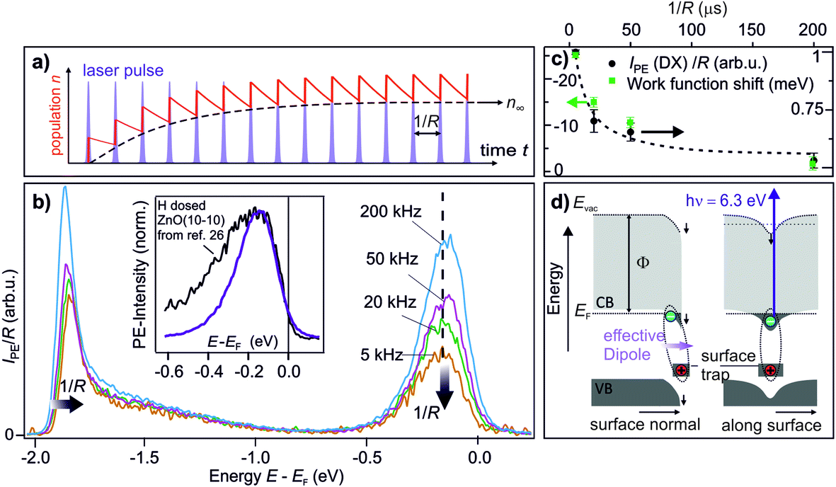 | ||
| Fig. 2 Central experimental evidence for long-lived defect excitons that act like shallow donors at the ZnO(10−10) surface. (a) Photoexcited states form a photostationary population if they have a lifetime that exceeds the inverse laser repetition rate 1/R. (b) Repetition-rate dependent PE spectra of as-prepared ZnO(10−10). The intensity of the peak below EF is reduced as the repetition rate is lowered, revealing that it is a photostationary state. Concomitantly, the secondary edge shifts up. Inset: comparison of the PE spectrum of the photostationary state to a PE spectrum with H adsorbed at the ZnO(10−10) surface. The spectrum is taken from ref. 26, with kind permission from the author. (c) Work function change and intensity of the peak below EF as a function of 1/R, extracted from the raw data in (b). The dashed line is a guide for the eye. The data points represent the average from repeating the experiment three times; error bars represent one standard deviation. (d) Interpretation of the observation: optical excitation of deep defects at the ZnO surface creates DX. Left hand side: the complex at the surface has a dipole moment which reduces the work function. Right hand side: the electron is laterally localized due to the hydrogenic potential of the surface defect, as discussed in Section 3.5. The metastable defect excitons are created and detected by laser photons with hν = 6.3 eV as they form a photostationary state. | ||
The PE spectra in Fig. 2b exhibit marked changes upon changing R. Firstly, the PE-intensity of the state below EF drops by about 50% upon lowering the repetition rate from 200 kHz to 5 kHz. The reduction of the PE intensity with lowering R means that the shallow donor-like electronic population below EF is photostationary, with a lifetime in the order of the inverse laser repetition rate 1/R (5–200 μs). Secondly, at the same time as the PE intensity due to the electron population below EF drops, lowering R also affects the secondary electron cut-off. The raw data in 2b unveils a systematic upward shift of the secondary electron cut-off when lowering R. The shift of the secondary electron cut-off, i.e. the sample work function, together with the PE intensity of the peak below EF, is shown in Fig. 2c as a function of the temporal distance between two laser pulses 1/R. The work function is 25 meV lower when the PE-intensity below EF is at its maximum (at R = 200 kHz) with respect to its minimum value (at R = 5 kHz). Evidently, the photostationary electron population is connected to an equally long-lived work function reduction. Also, this is in line with H adsorption at the ZnO surface.24 Both the photostationary electron population with a spectral signature similar to H dopants, as well as the concomitant work function reduction, suggest that the ZnO surface is photostationary n-type doped.
To explain the above observations, metastable free excitons can clearly be excluded, as they are inconsistent with a localization at the surface. Instead, surface-bound electrons and a work function reduction would be readily explained by the formation of DX upon photoexciting deep defects at the ZnO surface: photoexcitation leads to comparably delocalized electrons in the ZnO CB bound to localized hole states at the surface. Thus, an effective dipole is formed, which points outward the surface normal and lowers the work function (left hand side of Fig. 2), as upon the chemical doping of oxide surfaces.24 Alternatively, the photostationary n-type surface doping could be explained by excitons formed after cross band gap excitation, where the hole is localized at the surface due to polaron formation. Hole polarons with lifetimes up to minutes have been observed in ZnO.37 What discriminates these two cases is the origin of the photoexcited electrons, which are either VB states or deep defects in the ZnO band gap. Therefore, to identify the DX, we test whether cross-band gap excitation is necessary for creating the photostationary state or if sub-band gap photons are sufficient.
3.2 Photon energy dependency for the identification of the deep defects
Deep defects feature an occupied state within the band gap of semiconductors, cf.Fig. 1c. Hence, to photoexcite them, light with a photon energy below the fundamental band gap is sufficient. In order to see whether the photostationary state can be created with below band gap excitation, we perform photon energy-dependent pump–probe experiments. Pump laser pulses with photon energies below and above the band gap are used. The photon energy of the probe laser pulses is kept at 6.2 eV, i.e. above the sample work function, to be able to detect population changes below the Fermi energy EF, cf. the energy level diagram in Fig. 2d.Fig. 3a presents a typical pump–probe experiment, here using a pump photon energy of 3.2 eV. The PE intensity in false colors as a function of pump–probe delay in picoseconds (bottom) and energy (left) is shown. The photostationary signal at negative pump–probe delays was subtracted from the data in order to show the ultrafast dynamics of the photoinduced PE intensity due to the pump laser beam. Upon arrival of the pump laser at time zero, an abrupt rise of the PE intensity below EF is observed. The ultrafast rise and decay dynamics will be discussed later in Section 3.3. The energy of the pump-induced signal overlaps with the photostationary state observed in the steady state spectra. A part of the pump-induced signal also survives the inverse laser repetition rate, because adding the pump laser beam leads to an increase of the photostationary signal at negative pump–probe delays (not shown). As the photon energy of the pump laser pulse is, at 3.2 eV, significantly below the band gap of ZnO (3.4 eV), this shows that the photostationary state is populated from in-gap states, see the inset in Fig. 3a. It cannot originate from metastable electrons bound to polaronic VB holes at the ZnO surface, because such excitons require at least excitation at the free exciton resonance (3.38 eV at T = 4 K; 3.31 eV at T = 295 K (ref. 35)).
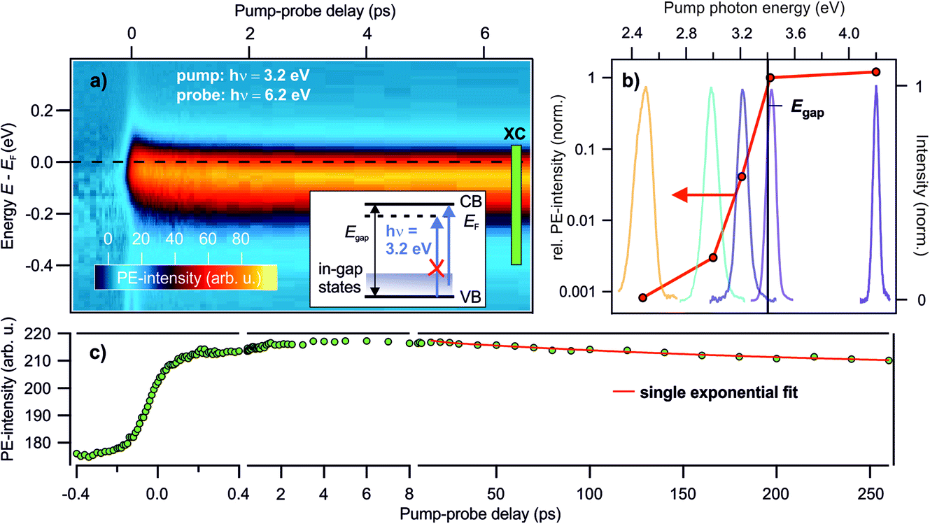 | ||
Fig. 3 Photon energy-dependent time-resolved PE measurements using hν = 6.2 eV as the probe photon energy and pump photon energies between 2.5–4.2 eV. (a) False color representation of the pump-induced population change as a function of the pump–probe delay and energy, with a pump photon energy of hν = 3.2 eV. The photostationary state was subtracted from the data to show the ultrafast intensity evolution around EF. Inset: energy level diagram showing that no excitations across the band gap are allowed for hν = 3.2 eV, but only from in-gap states. (b) Signal increase at positive with respect to negative delays according to eqn (1) for different pump–photon energies. The action spectrum shows that a photon energy of at least 3.0 eV is necessary to populate the state below EF. The colored lines are the laser spectra of the pump laser pulses to indicate photoexcitation below and above Egap. (c) Pump-induced PE intensity around EF resulting from integration across the box ‘XC’ indicated in (a) for a larger delay window up to 260 ps. The red line is a fit with a single exponential decay: I = I0![[thin space (1/6-em)]](https://www.rsc.org/images/entities/char_2009.gif) e−Δt/τd + offset. e−Δt/τd + offset. | ||
To determine the energetic position of the in-gap states, we tuned the pump photon energy over a wide range, from 2.5 eV to 4.2 eV. Fig. 3b displays (in red) the pump-induced signal increase at −0.3 to 0 eV with respect to EF evaluated at a positive pump–probe delay of 1 ps with respect to a negative delay of −1 ps. The signal increase is shown on a logarithmic scale versus the pump–photon energy and is determined from the non-background subtracted data according to
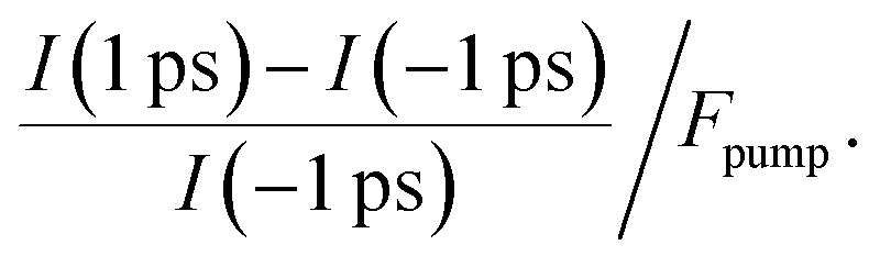 | (1) |
The energetic position of defects is characteristic of their chemical nature, hence the above result may be used to identify the defect species at the ZnO surface. Amongst the native defects, the oxygen vacancy is the only deep donor.38,39 According to hybrid DFT calculations,40 the oxygen vacancy in ZnO is located just above the VB edge, at 0.4 eV above the VB maximum or 3.0 eV below the CB minimum. This coincides with the above-determined position of the in-gap states. In fact, the action spectrum in Fig. 4b is also in agreement with the optical absorption of samples with deliberately added oxygen vacancies.41 This suggests that the origin of the in-gap states is oxygen vacancies. As an alternative to native defects, impurities or defect complexes could be the origin of the deep defects. A Zn vacancy bound to two H impurity atoms was recently predicted to feature a metastable state that could also cause PPC, as could oxygen vacancies.42 In order to finally identify the chemical nature of the involved defects, the next section shows how the defects are created.
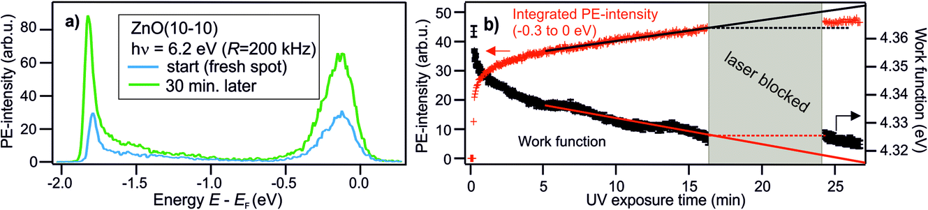 | ||
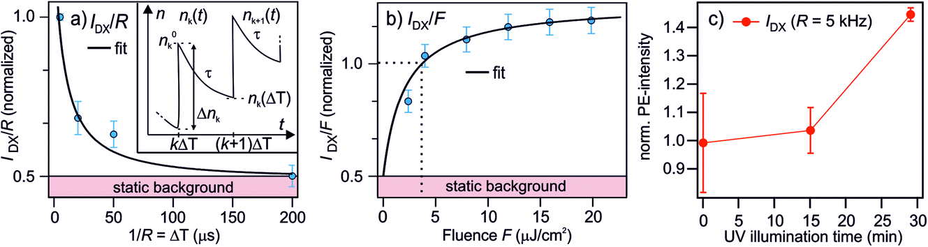
| Fig. 4 Change of the PE spectra as a function of UV exposure time. (a) PE spectra recorded with hν = 6.3 eV directly after addressing a previously not illuminated spot on the as-prepared ZnO surface (blue curve) and after 30 min of continuous UV illumination (green curve). (b) Work function reduction and rise of PE intensity in the energetic region −0.3 to 0 eV with respect to EF as a function of UV exposure time, extracted from the PE data. The two quantities change concomitantly. The solid and dashed lines are guides for the eye. The grey box indicates that the laser is blocked (during minutes 17–24). | ||
3.3 Relation to UV illumination-induced defects
Defects, impurities and defect complexes can be present in ZnO due to the growth process as well as the preparation of the surface due to sputtering and high temperature annealing.29,43,44 After the sample preparation, additional defects can be created by UV illumination; it has been shown by mass and X-ray spectroscopy that oxygen is removed from the ZnO surface upon UV illumination, making the surface more Zn-rich.21,45 Therefore, to figure out if oxygen vacancies are indeed the origin of the deep defect levels, we investigate if the photoresponse changes as a function of the UV illumination time.Fig. 4a shows the PE spectra recorded with hν = 6.2 eV at two different times. The blue spectrum is measured just after preparation of the sample surface and the green one after 30 minutes of UV illumination. The two spectra are clearly very different. The state below EF has increased by a factor of 2. The secondary edge, i.e. the sample work function, has shifted down. Fig. 4b shows these changes in more detail, measured across 30 min. Both spectral features have the same temporal evolution. After an initial non-linear rise, both the PE intensity increase below EF and the work function drop vary linearly. It is also illustrated that the change is not present when the laser (i.e. the UV illumination) is blocked, between minute 17 and 24; there, the work function does not drop further. The PE intensity below EF increases slightly during this time but clearly not at the same rate as before. The observed change of the PE spectra, i.e. the rise of the peak below EF and the drop of the work function, are readily explained by an increased number of DX as the density of deep defects at the surface is increased by the UV illumination. The small effect that happens in the dark may be due to the adsorption of residual gas present even in the UHV environment, such as H.46
An alternative scenario that would explain the growth of the DX signal during UV illumination is the buildup of the population of the photostationary state at a given defect density caused by repeated photoexcitation with subsequent laser pulses (see Fig. 2a). We can differentiate this accumulation effect from the increase of the deep defect density itself by inspecting the DX signal created with an individual laser excitation event and how it changes with UV illumination time. Pump–probe spectroscopy enables us to measure this, as the pump laser pulse also creates DX that decay faster than the inverse laser repetition rate (see the discussion of the ultrafast dynamics in the next section). We find that the number of these fast-decaying DX also increases upon UV illumination and does so with a similar rate as the photostationary population on a timescale of minutes to hours.33 This unambiguously shows that, on these long timescales, the UV illumination enhances the number of states that can be photoexcited with a single laser pulse, i.e. the density of deep defects at the ZnO surface. However, we note that the buildup of the photostationary state due to subsequent laser pulses may be responsible for the initial nonlinear change of the PE spectra that we observe in the first minute in Fig. 4b.
Based on the surface photolysis observed in the literature, the most likely deep defect created by UV illumination is the oxygen vacancy, as opposed to a defect complex involving a Zn vacancy. Hence, due to both their energetic position in the band gap, as well as their creation by UV illumination, we attribute the deep defects to oxygen vacancies.
3.4 Lifetime of the DX
The previous three sections showed that DX are excited at the ZnO surface, as we found (i) a photoexcited electronic population bound to a positive charge at the ZnO surface, which leads to a work function reduction, (ii) it is possible to photoexcite the state with below band gap photons and (iii) the population increases upon enhancing the surface defect density due to UV illumination. The DX are shallow donor-like, as they have a similar spectral signatures to those observed upon doping with H. In this section, we investigate the timescales associated to the DX dynamics.The pump–probe measurements introduced in Section 3.2 unveil the decay dynamics of the DX on ultrafast timescales. Fig. 3c displays the integrated intensity around EF. The buildup of the population is a two-step process consisting of a fast rise happening within the time-resolution of the experiment (<100 fs), followed by a slower process with a duration of several picoseconds. Subsequently, the DX start decaying on a timescale of hundreds of picoseconds. This is analogous to the case of using cross band gap excitation with 3.4 eV, which we reported in ref. 25. In line with our previous publication, the fast rise is attributed to the direct excitation of in-gap states at the ZnO surface and the subsequent DX formation, which occurs on screening timescales. The picosecond rise is attributed to the trapping of bulk or sub-surface holes at the surface. As photoexcited electrons are bound to the holes in an excitonic state, this enhances the number of DX at the surface and, hence, the photoemission signal below EF. This interpretation is also consistent with oxygen vacancies, which are predicted to lie at lower energies in the bulk than at the surface,47 thus energetically favoring the accumulation of holes in surface states. Eventually, the DX start recombining, which leads to the decay of the PE intensity on a timescale of hundreds of picoseconds. A single exponential fit gives τd = 250 ± 80 ps, also in agreement with our previous work.25
However, a significant portion the PE intensity decays more slowly, clearly surpassing the time window accessed in the pump–probe scans (cf.Fig. 3c). These DX eventually form the photostationary state as they live longer than the inverse laser repetition rate. In order to determine their lifetime, femtosecond pump–probe spectroscopy cannot be used. Instead, as shown in the following, the lifetime can be determined from the R dependency presented in Section 3.1, combined with an adequate model and supplementary laser fluence-dependent measurements.
An increase of the pulse-to-pulse distance ΔT = 1/R gives the photoexcited population more time to relax before the next laser pulse arrives (cf.Fig. 2a). However, the intensity decay in Fig. 2c does not directly reflect the lifetime of the DX as the laser-induced population and depopulation occurs every time a laser pulse arrives, leading to a complex intensity change of the photostationary state as a function of 1/R. In the following, we develop the simplest possible model that describes our experimental observations. To do so, we need to consider three contributions to the population dynamics: the photoexcitation of new DX, the depopulation by photoemission from the DX state, and the decay of DX on μs-timescales. Firstly, each laser pulse leads to an increase of the population by αN, where N is the total number of deep defects that can be excited. α < 1 is the population probability, which is assumed to be proportional to the laser fluence F, with an unknown factor a, i.e.
| α = aF. | (2) |
Secondly, as the population is probed in PE spectroscopy, electrons are removed from the state each time a laser pulse arrives. This happens with the depopulation probability
| β = bF, | (3) |
| Δnk = αN − βnk−1(ΔT), | (4) |
| nk(t) = n0ke−(t−tk)/τ, | (5) |
 | ||
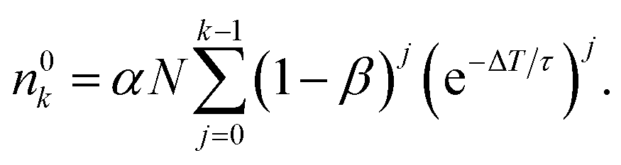
| Fig. 5 Measurements and model to determine the lifetime of the photostationary DX. (a) The PE intensity of DX as a function of the inverse laser repetition rate 1/R = ΔT, reproduced from 2c. Inset: illustration of the notation used in the model to calculate the photostationary population. (b) The PE intensity of DX as a function of the laser fluence F (R = 200 kHz). The black lines in (a) and (b) are global fits with eqn (7) and (8). Both data sets are normalized to the PE intensity at R = 200 kHz and the fluence used in the R-dependent measurements, which is F = 3.6 μJ cm−2. (c) The PE intensity of DX at R = 5 kHz as a function of UV illumination time. The rising trend of IDX(5 kHz) suggests that the ‘static background’ indicated in (a) and (b) is resulting from the photoexcitation of defects created by UV illumination as well, but with a lifetime ≫1/R (see text). | ||
n 0 k is calculated iteratively for each laser pulse. This leads to the sequence shown in Table 1. For the population after the k-th laser pulse, one can identify the geometric series
 | (6) |
e−ΔT/τ is the population just before the k + 1-th laser pulse, which depopulates nk(ΔT) and populates new DX according to eqn (4)
| k | n 0 k |
n
k
(ΔT) = n0ke−ΔT/τ |
|---|---|---|
| 0 | 0 | 0 (sample is in equilibrium) |
| 1 | n 0(ΔT) + Δn1 = αN |
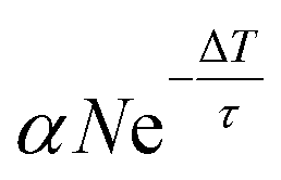
|
| 2 |
|
|
| 3 | … | … |
For many pulses, k → ∞, so the population becomes33
 | (7) |
This is the DX population in the photostationary state, which depends on the inverse repetition rate ΔT = 1/R, as well as on the laser fluence F.
Importantly for the comparison to the experiment, b can be directly determined from pump–probe spectroscopy by choosing a pump photon energy above the work function. The DX dynamics monitored with the probe laser pulse are similar to Fig. 3c, where a pump photon energy below the work function is used, but with the crucial difference that the DX signal first drops at time zero, which is due to the depopulation of the DX by photoemission due to the pump laser pulse. The drop in PE intensity can be directly related to b, resulting in b = 0.034 ± 0.017 cm2 μJ−1.33 The conservatively estimated error bar for b is 50%. In order to fit the detected PE intensities, it should be noted that they are proportional to the number of incident photons per time R × F, i.e.
| IDX ∝ RF(n∞ + n0). | (8) |
The model is now fitted to the experimental data in Fig. 5. Panel (a) shows the PE intensity of the DX divided by R at constant F as a function of 1/R = ΔT and panel (b) shows IDX/F as a function of F for constant R. Qualitatively, a decay and a rise with increasing fluence is observed, respectively, tending towards saturation. The black lines are global fits with eqn (7) and (8), yielding τ = 77 ± 45 μs and n0 = 0.52 ± 0.1. Note that the DX population saturates at high fluence due to a balance between population and depopulation, as eqn (7) approaches a constant for large α and β.
n 0 is invariant under F and ΔT and amounts to about half the PE intensity at 1/R = 5 μs; the PE intensity due to n0 is indicated as 'static background' in Fig. 5a and b. This shows that either an additional photoexcitation-independent state isoenergetic with the DX is present or that a part of the DX survives much longer than the μs window accessed with the R dependency. For the identification of the source of n0, it is helpful to recognize that the time-dependent DX population n∞(ΔT) has decayed after 200 μs (cf.Fig. 5a) and, therefore, IDX(5 kHz) represents the quasistationary contribution n0. To identify whether n0 results from even longer-lived DX or is an entirely new, independent feature, we examine the long-time evolution of IDX(5 kHz) in Fig. 5c. Note that we have shown above that continuous UV illumination leads to a growing number of deep defects and, thus, DX. Fig. 5c clearly indicates that the n0 population also rises as the sample is exposed to UV light. This rising trend shows that n0 increases as the surface defect density is enhanced. It, thus, seems highly likely that the quasistationary population n0 results from DX with lifetimes on ms-timescales or longer. The origin of the different lifetimes of the DX will be discussed in Section 4.
3.5 Metastable metallization
As explained in the Introduction, a crucial property of shallow donor dopants is their influence on the electrical conductivity of semiconductors. At low densities, the electrons are localized at the impurity sites, inducing thermally activated conductivity, while the electrons delocalize at a sufficient density into a metallic band as the Mott semiconductor-to-metal transition occurs. The DX discovered in this work have a similar spectral signature as H dopants, i.e. shallow donors. However, do they also lead to metallic conductivity? In our previous publication,25 we have shown that the surface of ZnO can be reversibly metallized by the photoexcitation of deep defects on an ultrashort timescale. The temporal variation of the density of photoexcited defects leads to the dynamic evolution of localized electrons into a parabolic band, and a subsequent localization within hundreds of picoseconds (with τd, the picosecond decay of the DX). Here, we expand these results to the photostationary DX and show that the ZnO surface becomes a metastable metal at sufficient densities of photoexcited deep defects.Fig. 6a presents the steady-state angle-resolved PE spectrum around EF, detected with 6.3 eV laser photons. The measurement is recorded after 1.5 hours of UV illumination of the as-prepared sample. The data shows the DX feature ca. 100 meV below EF and with a width of several hundred meV. The angular distribution of this state is symmetric and does not exhibit an apparent curvature, indicative of localized states. Fig. 6b shows the angle-resolved PE spectrum after 6 hours of UV illumination. Within this time span, the PE-intensity from the DX increased by a factor of about 4 (not shown). In contrast to the spectrum after 1.5 hours of UV illumination (Fig. 6a), the PE intensity is now directly adjacent to EF, appears broadened and assymmetric, i.e. it has apparently a more pronounced curvature at lower energies, and seems to be cut by EF, more like a metallic band than localized states.
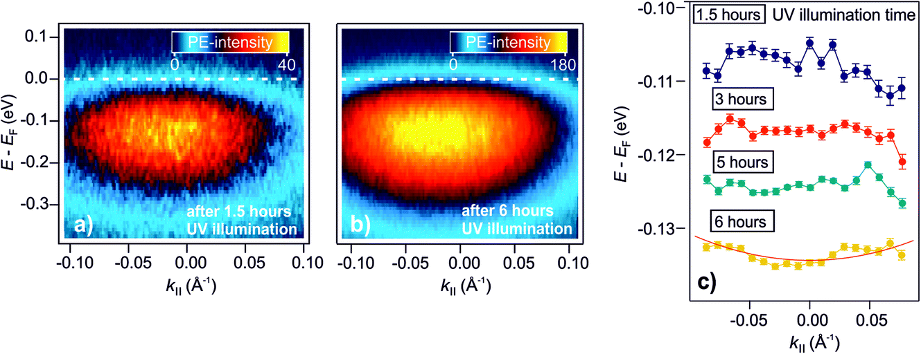 | ||
| Fig. 6 Metastable metallization of the ZnO surface due to DX. (a) and (b) Angle-resolved PE spectra after 1.5 hours and 6 hours of UV illumination of the as-prepared ZnO(10−10) surface, respectively. After 1.5 hours, the PE intensity shows a dispersionless feature due to localized electrons. (b) After 6 hours, the PE intensity exhibits a more pronounced curvature at lower energies and seems to be cut by EF, more like a metallic band than localized states. (c) Overview of the evolution of the peak maxima over 6 hours. The traces are vertically offset for clarity. The red line is a free electron-like parabola (eqn (9)). | ||
To inspect the dispersion change of the DX feature as a function of UV illumination time in more detail, the apparent dispersion is evaluated by determining the position of the peak maximum of the PE intensity at different k∥. This is done by fitting an asymmetric Gaussian function to the spectra (evaluation procedure not shown, see ref. 33 for details). The so-determined peak maxima are plotted in Fig. 6c for angle-resolved PE spectra recorded after 1.5, 3, 5 and 6 hours of UV illumination. The traces are vertically offset by ca. 0.01 eV for clarity. After 1.5 hours, the peak maxima show a slight tendency toward a negative curvature. This has been observed before in the context of localized states and is attributed to the simultaneous sampling of electrons with a different degree of localization and, hence, different binding energies and momentum spread.32 For longer UV illumination times, the dispersion starts to flatten and evolve into a parabolic dispersion with positive curvature. The red line on top of the trace after 6 hours is the plot of a free electron-like parabola,
 | (9) |
We expect that even longer UV illumination times lead to more shallow donor-like DX and, in analogy to the density-dependent evolution on ultrafast timescales,25 to a lowering of the effective mass. Eventually, the effective mass should follow the critical behaviour for a shallow donor Mott semiconductor-to-metal transition.
4 Discussion
4.1 DX–shallow donor analogy
Can photoexcitation truly act like chemical doping? Chemical doping by shallow donors features additional electrons which are first localized (leading to thermally activated conduction) and then form a metallic impurity band as the doping density crosses the Mott limit. These two conditions must be met by photoexcitation in order to justify the term “photodoping”. From the conceptual comparison given in the Introduction, it is expected that DX might act like shallow donors, however, so far, it was unknown to what extent the analogy holds true, as photodoping by DX was previously only inferred from transport measurements for a chemically pre-doped sample by Katsumoto et al.13 Using photoelectron spectroscopy, we show above that ZnO exhibits a photoinduced localized electronic state below EF and unveil – by the associated work function reduction – that it is bound to a positive surface charge. The state can be excited with laser photon energies slightly below the fundamental band gap and grows as the defect density at the surface is increased. Hence, the positive surface charge is located at a deep defect at the surface. In other words, we directly observe DX. The effect of the photoexcitation is by all means comparable to chemical doping of the ZnO surface with shallow donors: firstly, the spectral signature of the electronic state below the CB (at 150 meV below EF) overlaps with that of adsorbed H, and the work function reduction is also in line with the latter. Secondly, the electronic state is first localized and then evolves into a metallic band at a sufficient density of DX. Remarkably, we find that the metallization can be performed on two different timescales by controlling the DX density: For low defect densities, i.e. short UV illumination times after sample preparation, the metastable (μs to ms and above) component of the DX is localized. We observe this for all photoexcitation fluences (not shown), consistent with the finding that the photostationary population saturates as a function of laser fluence (cf. Section 3.4). This is the initial state for the ultrafast metallization described previously,25 where an individual strong laser pulse enhances the DX density above the Mott limit. The system returns to the semiconducting state within τd, the ultrashort decay of the DX, i.e. much faster than the inverse laser repetition rate. Beyond varying the laser fluence, the DX population is enhanced by the increase of the defect density due to continuous UV illumination. This also means an increase of the photostationary population, cf.eqn (7). At a sufficient defect density, the photostationary DX population renders the ZnO surface a metastable (photostationary) metal. Hence, the ZnO surface always becomes metallic when the DX density crosses the Mott limit, caused by an exciton Mott transition of DX. It is noteworthy that on both timescales (metastable as well as ultrashort), the Fermi energy EF of the metallic band equals the equilibrium EF (cf.Fig. 6b and ref. 25). Although photoexcitation drives the system into a non-equilibrium state, the resulting phase transition is equivalent to the equilibrium metallization by chemical doping. We suspect that this is due to the surface character of the photodoping and results from equilibration of the surface Fermi level with that of bulk ZnO. As charge accumulation layers of oxides can be as thin as 1 nm,24,48 charge exchange between the metallic state at the surface and the bulk happens on ultrafast timescales. In conclusion, the spectroscopic similarity to H doping, as well as the photoinduced semiconductor-to-metal transition in a nominally undoped ZnO sample, illustrates that DX are truly equivalent to shallow donors. This “photodoping” allows us to control the conduction properties of ZnO over at least 6 orders of magnitude in time, from ps to μs and even longer timescales.4.2 Relation to PPC
Persistent photoconductivity has been predicted theoretically to arise from photoexcited oxygen vacancies, creating shallow donor states.17 Although oxygen vacancies are widely accepted to be the source of PPC, many experimental studies explain the effect within the framework of equilibrium upward band bending. Moreover, as PPC lifetimes range from below seconds to hours and longer, it is still being discussed whether it is due to a single mechanism, i.e. photoexcited oxygen vacancies, or whether the photodesorption of adsorbed oxygen as alternative mechanism is at play.16The photodoping of the ZnO surface due to photoexcited oxygen vacancies reported in this work means that there must be photoinduced conductivity lasting as long as the DX live. We identified a species decaying with τd = 250 ps and two metastable species, one decaying within 77 μs and one exceeding the μs regime. Within the theory of photoexcited oxygen vacancies,17,19,38 the different lifetimes of the DX can be explained as follows: the ultrafast decay τd = 250 ps is likely to be attributed to direct recombination of photoexcited electron–hole pairs prior to forming the polaronic state, which prolongs the lifetime.17,38 Regarding the two metastable species, the theory unanimously predicts that the oxygen vacancies can be singly and doubly charged. Both charging states deform the lattice and thereby suppress electron–hole recombination, which leads to metastable states.17,19 Therefore, we tentatively assign the metastable species to the singly and doubly photoionized oxygen vacancies, respectively.
While our results directly demonstrate that the Mott transition of DX leads to photoconductivity on sub-second timescales, DX-driven PPC at longer times can be inferred indirectly, as outlined in the following. Our experiments indicate a long-lived, metastable part of the DX population that does not decay on μs timescales. These long lifetimes can be rationalized by considering that the defect-induced, metallic impurity band lies below the sample’s Fermi energy. This means that, on the one hand, any depopulation process beyond electron–hole recombination (e.g. thermal activation to unoccupied levels) will eventually be compensated by repopulation, as the electronic level will persist as long as the hole polaron remains. Electron–hole recombination, on the other hand, is highly unlikely, because no vertical transitions are available in conformational space due to the strong lattice deformation.17 Conceptually, this can be viewed in a Marcus-type picture for electron transfer,49 where the reorganization energy stored in the environment of the hole is so large that there is no free energy gain upon recombination with the electron. Such trapping of electrons below EF can easily lead to lifetimes of minutes, hours, or even days. Although we cannot determine this lifetime experimentally and, therefore, cannot provide direct evidence for PPC on these timescales, we would like to point out that the action spectrum in Fig. 3b for the surface metallization is nearly identical to the photon energy dependence of PPC creation in various samples with lifetimes up to hours and longer.14,16,20 In other words, as the minimum photon energies to create PPC or DX are 3.0–3.15 eV, consistent with the photoexcitation of oxygen vacancies, as discussed in Section 3.3, it seems highly likely that DX are also responsible for PPC on these long timescales. This conclusion is in agreement with the previous assignment by ref. 14, 20 and in opposition to ref. 16 which considered sub-band gap photoexcitation so close to the fundamental band gap as insufficient proof and only attributed the short-lived PPC to photoexcited oxygen vacancies. We believe that our experiments show clear evidence for photoexcited oxygen vacancies as the origin of PPC on timescales below seconds as well as on hours and longer, possibly due to single and double photoionization. The oxygen vacancies are created by UV illumination at the ZnO surface and are subsequently photoexcited into metastable shallow donor-like states, as predicted theoretically.
Beyond associating the fast and slow timescales of PPC with the photoexcitation of oxygen vacancies, our study, importantly, resolves that PPC due to DX must be understood by their shallow donor behaviour. As ZnO is photodoped at the surface, this leads to downward surface band bending and eventually to a metallic surface. The auxiliary condition of upward band bending at ZnO surfaces is not necessary to explain PPC. On the contrary, as DX may already be excited under daylight illumination, ZnO surfaces are likely to always exhibit downward band bending. The literature suggests that the photoinduced downward shift of the surface potential of ZnO, inferred from a downward shift of the core levels22 and the work function,21 is evidence for equilibrium upward band bending. In this picture, upward surface band bending leads to a separation of the charges, and a transient polarization field at the surface mitigates the band bending (surface photovoltage). Our work shows that this circuitous view of equilibrium surface band bending abolished by photoexcitation can be replaced by the plain photoexcitation of DX, as these provide one single, simple explanation of all the phenomena discussed above: DX induce downward surface band bending, also known as photovoltage inversion,50 which goes along with a downward shift of the surface potential. They also undergo a Mott transition and render the ZnO surface metallic on ultrafast and macroscopic timescales.
The above conclusion that ZnO surfaces tend to have downward band bending has important implications for ZnO devices, such as ZnO-based hybrid solar cells, for example. In these solar cells, a current is generated after the injection of photogenerated electrons from an organic adlayer into ZnO. The assumption of upward band bending led to the conclusion that ZnO is a good substrate as electrons would be driven away from the interface, would have long lifetimes and could thus contribute to the current.22,51 Downward surface band bending due to DX as observed in this work might actually have the opposite effect, i.e. the trapping of injected charges at the interface and hindering of charge extraction. This is consistent with reports of ZnO-based hybrid solar cells that become less efficient upon photoexcitation with UV light, which was attributed to UV illumination-induced surface states.52,53 The suppression of ZnO deep defect states due to surface modification by adlayers was found to increase the solar cell performance.52
The insights gained in this work are thus quite universally relevant to applications of ZnO, as the DX influence the electronic surface properties, inducing conductivity and downward band bending. We expect that DX are excited whenever ZnO is exposed to UV light and affect the electronic properties even very long after excitation.
5 Summary
In summary, static as well as time- and angle-resolved PE spectroscopy of ZnO(10−10) under UHV conditions allowed us to reveal the presence of photoexcited excitons with the hole at a deep defect site at the surface. The DX lead to a similar spectroscopic signature as that produced by chemical doping with H and cause a Mott semiconductor-to-metal transition at sufficient densities. Depending on the initial defect densities, the metallization can be short-lived or metastable, following the complex decay dynamics of the DX, which range from hundreds of ps to μs and even longer. The Fermi level in the surface metallic phase equals the equilibrium EF on ultrashort to metastable timescales, i.e. photoexcitation acts like chemical doping in thermodynamic equilibrium. The deep defects are created by UV illumination and feature an (occupied) energy level at <400 meV above the VB edge. These results are consistent with photoconductivity measurements of ZnO reported in the literature and strongly support that both short- and long-lived (persistent) photoconductivity arise due to photoexcited oxygen vacancies at the ZnO surface, which behave like shallow donors. The transient surface doping leads to downward band bending, as opposed to the usually assumed upward surface band bending in photoexcited ZnO.15,16,22,23 To the extent that we can judge with PE spectroscopy, we conclude that the conceptual analogy between shallow donors and optically excited DX holds true, ranging from quasi-equilibrium metallization and critical behaviour on ultrafast timescales to metastable n-type doping at the ZnO surface. Beyond these fundamental research aspects, our results are also relevant to ZnO-based devices. DX may be created without knowledge, simply by daylight exposure, leading to photoinduced conductivity and surface band bending with effects, for example, on ZnO solar cells. In addition, the intentional photoexcitation of DX can be used for the optical control of the conductive properties of ZnO even on ultrafast timescales. Lastly, we expect that photodoping by DX can also be reached in other semiconductor compounds with deep defect states, including complex materials.54Author contributions
L. G. and S. V. did the experiments, L. G. analyzed the data, L. G. and J. S. wrote the manuscript. J. S. supervised the work. All authors contributed to the discussion and interpretation of the results.Conflicts of interest
There are no conflicts to declare.Acknowledgements
This work was funded by the Deutsche Forschungsgemeinschaft (DFG, German Research Foundation)-Project-ID 182087777-SFB 951. S. V. would like to thank the Max Planck Research Society for a Max Planck Postdoctoral Fellowship. The authors thank J.-C. Deinert for providing the reference spectrum (H dosed ZnO) in the inset of Fig. 2b.Notes and references
- N. F. Mott, Semiconductor-to-metal Transitions, Taylor & Francis, London, 1st edn, 1974 Search PubMed.
- G. Yu, C. H. Lee, A. J. Heeger, N. Herron and E. M. McCarron, Phys. Rev. Lett., 1991, 67, 2581–2584 CrossRef CAS PubMed.
- D. N. Basov, R. D. Averitt, D. Van Der Marel, M. Dressel and K. Haule, Rev. Mod. Phys., 2011, 83, 471–541 CrossRef CAS.
- C. Giannetti, M. Capone, D. Fausti, M. Fabrizio, F. Parmigiani and D. Mihailovic, Adv. Phys., 2016, 65, 58–238 CrossRef CAS.
- A. Cavalleri, M. Rini, H. H. Chong, S. Fourmaux, T. E. Glover, P. A. Heimann, J. C. Kieffer and R. W. Schoenlein, Phys. Rev. Lett., 2005, 95, 237401 CrossRef PubMed.
- D. Wegkamp, M. Herzog, L. Xian, M. Gatti, P. Cudazzo, C. L. McGahan, R. E. Marvel, R. F. Haglund, A. Rubio, M. Wolf and J. Stähler, Phys. Rev. Lett., 2014, 113, 216401 CrossRef PubMed.
- S. Iwai, M. Ono, A. Maeda, H. Matsuzaki, H. Kishida, H. Okamoto and Y. Tokura, Phys. Rev. Lett., 2003, 91, 057401 CrossRef CAS PubMed.
- J. Quereda, T. S. Ghiasi, C. H. Van Der Wal and B. J. Van Wees, 2D Materials, 2019, 6, 025040 CrossRef.
- L. V. Scalvi and C. F. Bueno, J. Phys. D: Appl. Phys., 2020, 53, 033001 CrossRef CAS.
- P. A. Cox, The Electronic Structure and Chemistry of Solids, Clarendon Press, 1st edn, 1987 Search PubMed.
- Y. Zhang, Chin. Phys. B, 2018, 27, 117103 CrossRef CAS.
- Y. Zhang and J. Wang, Phys. Rev. B: Condens. Matter Mater. Phys., 2014, 90, 155201 CrossRef.
- S. Katsumoto, F. Komori, N. Sano and S. Kobayashi, J. Phys. Soc. Jpn., 1987, 56, 2259–2262 CrossRef CAS.
- R. J. Collins and D. G. Thomas, Phys. Rev., 1958, 112, 388 CrossRef CAS.
- J. Bao, I. Shalish, Z. Su, R. Gurwitz, F. Capasso, X. Wang and Z. Ren, Nanoscale Res. Lett., 2011, 6, 404 CrossRef PubMed.
- M. Madel, F. Huber, R. Mueller, B. Amann, M. Dickel, Y. Xie and K. Thonke, J. Appl. Phys., 2017, 121, 124301 CrossRef.
- S. Lany and A. Zunger, Phys. Rev. B: Condens. Matter Mater. Phys., 2005, 72, 035215 CrossRef.
- S. Lany and A. Zunger, Phys. Rev. Lett., 2007, 98, 045501 CrossRef PubMed.
- A. Janotti and C. G. Van De Walle, Appl. Phys. Lett., 2005, 87, 122102 CrossRef.
- P. Liu, G. She, Z. Liao, Y. Wang, Z. Wang, W. Shi, S.-T. Lee and D. Chen, Appl. Phys. Lett., 2009, 94, 063120 CrossRef.
- R. Gurwitz, R. Cohen and I. Shalish, J. Appl. Phys., 2014, 115, 033701 CrossRef.
- B. F. Spencer, D. M. Graham, S. J. O. Hardman, E. A. Seddon, M. J. Cliffe, K. L. Syres, A. G. Thomas, S. K. Stubbs, F. Sirotti, M. G. Silly, P. F. Kirkham, A. R. Kumarasinghe, G. J. Hirst, A. J. Moss, S. F. Hill, D. A. Shaw, S. Chattopadhyay and W. R. Flavell, Phys. Rev. B: Condens. Matter Mater. Phys., 2013, 88, 195301 CrossRef.
- P. M. Wojcik, L. D. Bastatas, N. Rajabi, P. V. Bakharev and D. N. McIlroy, Nanotechnology, 2021, 32, 035202 CrossRef CAS PubMed.
- J.-C. Deinert, O. T. Hofmann, M. Meyer, P. Rinke and J. Stähler, Phys. Rev. B: Condens. Matter Mater. Phys., 2015, 91, 235313 CrossRef.
- L. Gierster, S. Vempati and J. Stähler, Nat. Commun., 2021, 12, 978 CrossRef CAS PubMed.
- J.-C. Deinert, PhD thesis, Technische Universität Berlin, 2016.
- C. Wöll, Prog. Surf. Sci., 2007, 82, 55–120 CrossRef.
- S.-H. Na and C.-H. Park, J. Korean Phys. Soc., 2009, 54(9(2)), 867–872 CrossRef CAS.
- U. Diebold, L. V. Koplitz and O. Dulub, Appl. Surf. Sci., 2004, 237, 336–342 CrossRef CAS.
- J. Stähler and P. Rinke, Chem. Phys., 2016, 485–486, 149–165 Search PubMed.
- A. Damascelli, Phys. Scr., 2004, T109, 61–74 CrossRef CAS.
- U. Bovensiepen, C. Gahl and M. Wolf, J. Phys. Chem. B, 2003, 107, 8706–8715 CrossRef CAS.
- L. Gierster, PhD thesis, Technische Universität Berlin, 2021.
- K. Ozawa, K. Sawada, Y. Shirotori and K. Edamoto, Phys. Rev. B: Condens. Matter Mater. Phys., 2003, 68, 125417 CrossRef.
- C. Klingshirn, J. Fallert, H. Zhou, J. Sartor, C. Thiele, F. Maier-Flaig, D. Schneider and H. Kalt, Phys. Status Solidi B, 2010, 247, 1424–1447 CrossRef CAS.
- C. Klingshirn, Semiconductor Optics, Springer Series in Materials Science, 4th edn, 2012 Search PubMed.
- H. Sezen, H. Shang, F. Bebensee, C. Yang, M. Buchholz, A. Nefedov, S. Heissler, C. Carbogno, M. Scheffler, P. Rinke and C. Wöll, Nat. Commun., 2015, 6, 6901 CrossRef CAS PubMed.
- A. Janotti and C. G. Van de Walle, Rep. Prog. Phys., 2009, 72, 126501 CrossRef.
- K. Ellmer and A. Bikowski, J. Phys. D: Appl. Phys., 2016, 49, 413002 CrossRef.
- C. H. Patterson, Phys. Rev. B: Condens. Matter Mater. Phys., 2006, 74, 144432 CrossRef.
- J. Wang, Z. Wang, B. Huang, Y. Ma, Y. Liu, X. Qin, X. Zhang and Y. Dai, ACS Appl. Mater. Interfaces, 2012, 4, 4024–4030 CrossRef CAS PubMed.
- Y. Kang, H. H. Nahm and S. Han, Sci. Rep., 2016, 6, 35148 CrossRef CAS PubMed.
- W. Göpel and U. Lampe, Phys. Rev. B: Condens. Matter Mater. Phys., 1980, 22, 12 CrossRef.
- S. Vempati, J. Mitra and P. Dawson, Nanoscale Res. Lett., 2012, 7, 470 CrossRef PubMed.
- J. Cunningham, E. Finn and N. Samman, Faraday Discuss. Chem. Soc., 1974, 58, 160–174 RSC.
- J.-C. Deinert, D. Wegkamp, M. Meyer, C. Richter, M. Wolf and J. Stähler, Phys. Rev. Lett., 2014, 113, 057602 CrossRef CAS PubMed.
- K. K. Korir, A. Catellani and G. Cicero, J. Appl. Phys., 2016, 120, 125301 CrossRef.
- S. McKeown Walker, A. De La Torre, F. Y. Bruno, A. Tamai, T. K. Kim, M. Hoesch, M. Shi, M. S. Bahramy, P. D. King and F. Baumberger, Phys. Rev. Lett., 2014, 113, 177601 CrossRef PubMed.
- R. A. Marcus, J. Chem. Phys., 1956, 24, 966–978 CrossRef CAS.
- L. Kronik and Y. Shapira, Surf. Sci. Rep., 1999, 37, 1–206 CrossRef CAS.
- B. F. Spencer, M. J. Cliffe, D. M. Graham, S. J. Hardman, E. A. Seddon, K. L. Syres, A. G. Thomas, F. Sirotti, M. G. Silly, J. Akhtar, P. O’Brien, S. M. Fairclough, J. M. Smith, S. Chattopadhyay and W. R. Flavell, Faraday Discuss., 2014, 171, 275–298 RSC.
- B. Wu, Z. Wu, Q. Yang, F. Zhu, T. W. Ng, C. S. Lee, S. H. Cheung and S. K. So, ACS Appl. Mater. Interfaces, 2016, 8, 14717–14724 CrossRef CAS PubMed.
- Y. Kim and B. Park, Nanoscale, 2018, 10, 20377–20383 RSC.
- W. Li, J. Shi, K. H. Zhang and J. L. Macmanus-Driscoll, Mater. Horiz., 2020, 7, 2832–2859 RSC.
Footnote |
| † Present address: Department of Physics, Indian Institute of Technology Bhilai, Raipur-492015, India. |
| This journal is © The Royal Society of Chemistry 2022 |