
 Open Access Article
 This Open Access Article is licensed under a Creative Commons Attribution-Non Commercial 3.0 Unported Licence
Micro/nanostructured gas sensors: the physics behind the nanostructure growth, sensing and selectivity mechanisms
N. K.
Chowdhury
and
B.
Bhowmik
 *
*
Thin Film Devices Laboratory, National Institute of Technology, Jamshedpur, India. E-mail: bb.cemk.ece@gmail.com
First published on 27th October 2020
Abstract
Micro/nano sensors based on oxide semiconductors have received much interest worldwide due to their remarkable electrical conductivity, good stability, wide range of dimensional structures, large-scale production potential, and cost effectiveness. The present review extensively investigates the physics behind the nanostructure growth, gas sensing, and selectivity mechanisms of different micro/nano-based devices. Mainly, planar, vertical, heterojunction, and thin film devices are discussed along with their pros and cons in relation to gas sensing and transport mechanisms. The sensing behaviours of such devices have been explained considering nanostructure morphology (particles and pore sizes), surface states (type of defect states and defect concentrations), and interfaces (intra- and inter-grain boundaries). Further, nanostructures with different dimensions, such as nanoparticles, nanowires, nanorods, nanoplates/nanosheets, nanotubes, hollow spheres, and nanoflowers, have also been taken under consideration.
Introduction
Micro/nano sensors are essential for detecting toxic polluting gases for controlling vehicle and industrial emissions, ensuring home security, and allowing environmental monitoring.1 Gas sensing technology based on surface acoustic wave (SAW), quartz micro-balance (QMB), gas chromatography mass spectrometry (GC-MS) and chemiresistors has received much attention in the last decade.2 Among these, metal oxide chemiresistive sensors (MOXChem) are mostly used in domestic, commercial, and industrial settings, due to their lower fabrication costs, ease of production, and compact size.1,2 In recent years, air pollution has become a major concern around the globe.3 The majority of air pollution is caused by toxic chemical and compounds involving NH3, O3, CO, CH4, etc.4 The location-specific detection of VOC molecules, especially those due to leakage, can possibly be used to control the pollution threat from chemical/drug industries and home appliances. Harmful pollutants based on oxide forms of nitrogen (like NO, NO2, and NOx), oxides of carbon (CO, CO2), ozone (O3), and suspended liquid particles in the atmosphere (many VOCs, such as methanol (CH3OH), ethanol (C2H5OH), acetone (CH3COCH3), benzene (C6H6), and toluene (C6H5CH3)) are responsible for harsh effects.5–8The performance of oxide-based sensors is controlled by their morphologies and structures. Improvements in sensor parameters, such as increasing the sensitivity, selectivity, and speed of reaction, through variations in nanostructure dimensionality have been a prime focus in recent years.3,4,10 For example, to achieve better selectivity for a particular species while employing oxide-based nanostructured sensors, some previously adopted strategies have been: (i) the incorporation of foreign elements, (ii) the use of hybrid composite materials as sensing materials, (iii) the variation of the sensor operating temperature, (iv) functionalization with noble metals as surface modifiers, and (v) the use of electronic nose/multi-sensor arrays examining gas fingerprints.1–10 The generic definitions of the different dimensional structures in the nanoscale regime are as follows: (i) when all three spatial dimensions (X, Y and Z) are in the nanometer range, this is known as 0D (zero-dimensional), e.g. nanoparticles and nanoclusters; (ii) when any two dimensions (either XY, YZ, or ZX) are in the nanometer range, e.g. nanotubes, nanorods, and nanowires, this is known as 1D (one-dimensional), (iii) when only one spatial dimension (either X, Y, or Z) is nanometric, such as in thin films or nanosheets, this is known as 2D (two-dimensional); and (iv) when there is a combination of 0D, 1D, and 2D elements in close proximity to form interfaces having all three dimensions, for example compact polycrystals with nanosized grains or 3D porous nanostructures, this is known as 3D (three-dimensional).11–13
The controlled growth of oxide nanostructures
High-quality nanostructures synthesized through feasible methods, such as sputtering, sol–gel and hydrothermal synthesis, spray coating, chemical vapor deposition (CVD), etc., with uniform sizes are widely used for different applications.14–23 Among the different synthesis methods, the hydrothermal process has the advantages of simplicity, good morphological control, low cost, and good long-term stability for the preparation of Ce-doped In2O3 nanomaterials.24 Solvothermal synthesis is another suitable method and it has been used for the synthesis of porous ZnFe2O4 nanospheres with the aid of heat treatment. Investigations revealed that gas sensors using this material showed improved selectivity for acetone at 200 °C.25 It was observed that solution-based approaches are more beneficial than physical processes for high-quality nanostructure preparation due to the facile and economic synthesis, large-scale production, and low reaction temperatures.14 However, the issue of nanostructure deformation during high-annealing-temperature treatment for the purpose of crystallization necessitates research into alternative sophisticated approaches.15 For example, vapor/liquid phase methods have been mostly adopted for 0D-nanoparticle or quantum-dot preparation, with specific exposed facets for gas sensing applications.10 Specific facets have different reaction kinetics toward different gases and, therefore, one can easily fabricate selective gas sensors based on materials with the growth of particular exposed facets. In this regard, template-based methods (soft or hard templates) based on organic or inorganic precursors have widely been accepted for fabricating mesoporous or hollow metal-oxide nanostructures.15Continuous pores with tunable size can easily be realized via this method. Most template-based approaches for oxide nanostructure preparation use PEO20–PPO70–PEO20 (P123), PEO106–PPO70–PEO106 (F127), and poly(ethylene-co-butylene)-block-poly(ethylene oxide) (KLE) as templates.15 The agent KLE helps to control synthesis processes, with the required micelle size, which depends on the block length, and a high decomposition temperature.26 KLE increases the stability at high temperature (600 °C). Zhou et al. investigated a direct synthetic strategy for mesoporous ZSM-5 zeolites via employing block copolymer templates like P123 and F127. It has been observed that when a gel-to-zeolite transformation happens, the Pluronic templates worked as a platform in order to maintain the spacing.27 Hard templates are used relatively less often because of etching problems. Representative hard templates, like poly(methyl methacrylate) (PMMA) spheres, silica spheres, and polystyrene (PS) spheres, have been used to obtain macroporous and mesoporous structures.3 After nanostructure formation, the outer template structure is removed either through annealing in ambient air or etching with NaOH (for SiO2 spheres) or CH2Cl2 (for PS spheres).3
Cutting-edge nanotechnology does not guarantee the compactness of nanodevices involving integrated circuits. However, it can guarantee the synthesis of highly ordered nanomaterials through accurate position control over a large surface area in an integrated circuit. In this regard, vertical stacking, self-assembly, or rubbing techniques may be used for precise alignment in a short time-span to realize highly integrated devices. Most nanoparticle suspension solutions have been uniformly distributed over layers by means of spray-coating or spin-coating techniques.15,16 However, when using such methods, the locations of the nanoparticles/microparticles are in question, as it is unclear how precisely they can be aligned. Sometimes, external temperature can be used to align the particle positions in a layer structure. A recent study found that polydimethylsiloxane (PDMS) can be used as a good aligner for microparticle positioning.8 The use of PDMS in association with rubbing techniques ensures precise particle positioning without any solvent and in a very short time span. Sensitivity can be enhanced to some degree in the case of materials prepared via a self-assembly process. Self-assembly-prepared SnO2 nanowires showed superior hydrogen detection abilities.1 An engineering approach that makes nanomaterials via self-assembly changes the surface states, which can effectively disrupt the intrinsic properties of a material and possibly enhance the gas-sensing performance compared to ultrasonically dispersed nanomaterials in ethanol.1
Generally, sputtering techniques are found to be the most promising methods for synthesizing p-type (Cr2O3, NiO, and CuO) ultrathin nanowire (thickness: ∼14 nm) arrays with a grain size of ∼5 nm (as shown in Fig. 1(b–d)).2 Ar+ ion bombardment and the presence of different transition metals (Cr, Ni, and Cu) in the sputtering chamber can easily result in the fabrication of different types of Cr2O3, NiO, and CuO nanowire arrays. The purpose of Ar+ ion bombardment is to control the etching of the transition metal to form oxide nanowires with different feature dimensions based on the etching rate. A study by Cho et al. revealed that a lower Ar+ ion bombardment etching rate with Cr metal results in shorter Cr2O3 nanowires with a height of ∼100–200 nm, whereas a higher etching rate with Cu and Ni produces nanowires with a height > 300 nm.2 Sputtering techniques offer better control over film thickness, with precise layer uniformity and good channel connectivity.3 Even better nanostructure uniformity may be achieved through atomic layer deposition (ALD).16 One of the most important benefits one can expect from ALD growth is the precise control of thickness at the atomic level. Sub-nanometer thickness control of oxide materials was achieved through the sequential use of self-limiting chemical reactions.16 In the ALD process, thin-film growth started with the nucleation of metal nanoparticles on the substrate surface. However, it is worth mentioning that a surface energy difference between the deposited material and the substrate leads to discontinuities in film growth. Therefore, to obtain film continuity, one should carry out repeat chemical reaction cycles on the surface.
 | ||
| Fig. 1 (a) The nucleation, precipitation, and growth of 2D nanosheet ensemble 3D spheres. (b) A TEM image of CuO revealing lattice spacing of 2.4 Å. (c) An FESEM image of a NiO nanowire array. (d) An FESEM image of Cr2O3 arrays (this figure has been reproduced from ref. 2 with permission from ACS Publications, copyright 2016). (e) An FESEM image of TiO2 nanoflowers (this figure has been reproduced from ref. 20 with permission from IEEE Transactions on Nanotechnology, copyright 2017). | ||
The nucleation and growth of homogeneous materials do not create many problems during sensor development. However, difficulties arise when assembling heterogeneous nanomaterials during sensor design and functional integration with microelectronic circuitry. The synthesis of heterogeneous structures, like CuO nanospikes, TiO2 nanotubes, and ZnO nanowires, on the same platform (substrate) possibly offers the development of an array of sensors for the screening of gases from mixtures of multiple gases.17 Therefore, one would not have to develop separate selective sensors for different gases. However, as already mentioned, gas-specific multi-sensor design on the same substrate was ruled out in an earlier effort due to poor contact between the electrode and sensing materials, poor controllability, and lower throughputs.17 Heterogeneous nanostructure-based multi-sensors synthesized via employing a hybrid combination of focused ion beam, hydrothermal, and liquid-phase deposition (LPD) techniques, which realized localized liquid-phase reactions through well-controlled thermal treatment, were found to offer a promising solution, mitigating the associated problems related to fabricating multiple sensors on the same platform.17
Obtaining ZnO nanoparticles with various shapes may be possible when employing zinc acetate as the metal precursor. Aggregated nanoparticles could possibly be converted to different shapes depending on the applied ultrasound energy.18 The ultrasonication of the nanoparticles for 15 min resulted in ZnO nanorods (having a diameter of 50 nm), whereas prolongation to 30 min produced 3D nanoflowers. Most solution-based ZnO-nanostructure growth happens in one dimensional direction due to the unique hexagonal crystal structure.14 Further, directing/capping agents play a major role in realizing different shapes and sizes of nanostructures. Directing/capping agents accelerate growth at certain faces via blocking some other faces of the crystal structure.19 Some commonly used capping agents for one-dimensional nanostructure growth are HCl, NaCl, H2C2O4, Na2SO4, and Li2SO4.10 It is believed that the governing factors determining the final crystal phase and nanostructure morphology are related to stabilizing cations (e.g. Na+, NH4+, Li+, etc.) and directing anions (e.g. SO42−, Cl−, C2O42−, etc).10 ZnO nanomaterials obtained via solution-based techniques offer polar as well as non-polar faces. However, most of the nucleation growth occurs at the polar faces. Growth initiated through the aggregation of ZnO nuclei towards polar faces (the axial direction) ultimately produces 1D nanostructures. On the other hand, nucleation towards non-polar faces (the equatorial direction) results in tabular nanostructures, such as nanoplates, nanosheets, etc. Growth at non-polar faces happens only when the passivation of polar faces is carried out via a growth modifier (suppressing growth in the axial direction).
Sol–gel derived TiO2 nanoflower synthesis occurs as follows (shown in Fig. 1(a) and (e)): titanium tetraisopropoxide, Ti(OPr)4, is the initial precursor, with anhydrous ethyl alcohol, deionized water, and HCl used as other chemicals.21 Deionised water, HCl, and ethyl alcohol were mixed and stirred vigorously. Then 0.4 M titanium tetraisopropoxide, Ti(OPr)4, was mixed gradually into the mixture for the hydrolysis of the precursor. The role of HCl is to control the condensation rate so that fast gelation can be prevented. The entire transparent mixture is then kept at room temperature for 30 days. Similarly, the substrate-dependent formation of different nanostructures has been observed.3,4,14 The hydrothermal synthesis of ZnO thin films produces hexagonal nanorods (∼200 nm in diameter) when the substrate is alumina ceramic tubes without Al nanolayers.12 On the other hand, the addition of Al nanolayers onto the alumina ceramic tubes resulted in ultrathin ZnO nanosheets (thickness: ∼15 nm).12 Nanostructures with numerous pores have received significant interest due to their unique gas sensing properties. Sensitivity improvement through pore-size control is possibly a similar powerful method to grain-size variation. Electrochemical anodization or an etching process produces a porous structure. Increasing the anodization voltage of Ti foil offers pores with longer lengths (etching towards the bulk material), whereas variations in the electrolyte concentration resulted in variations in the pore diameter.22 Zn-doped NiO crystals were synthesized via an electrolytic approach, and it was found that the process is advantageous due to excellent reproducibility, reversibility, stability, and selectivity toward NH3.28 The synthesis process for porous ZnFe2O4 nanospheres is as follows: 1 mmol of zinc nitrate hexahydrate (Zn(NO3)2·6H2O) and 2 mmol of ferric nitrate nonahydrate (Fe(NO3)3·9H2O) were dissolved into 40 mL of ethanol–ethylene glycol mixed solution. After stirring for a while, the solution was heated at 180 °C for 24 h and then left to cool down. Further, the remaining precipitate was collected and washed with deionized water and ethanol repeatedly and dried at 80 °C for 12 h. Lastly, the dried precipitate was heated at 400 °C for 2 h and porous ZnFe2O4 nanospheres were obtained.25
The hydrothermal synthesis of pure SnO2 showed randomly directed nanorods. Doping with foreign elements may or may not affect the nanostructure dimensionality, depending on the type of precursor available in solution. As evident in ref. 11, it is possible that the existence of Na+ cations from NaOH helps to retain the shape of the nanorods. However, the size of the nanorods is decreased and they are transformed to closely packed flower-like bunches (diameter: ∼3 ± 1 μm) upon the addition of Ni particles to solution.13 Precise morphology evaluations further confirm the nanosheet-like (thickness: ∼20 nm) petal structures of the nanoflowers, with well-defined lattice fringes; the (110) and (101) lattice planes show distances of 0.337 nm and 0.265 nm, respectively.11 Similarly In2O3 porous nanospheres with Ce dopant were synthesized via employing a low-cost simple hydrothermal process. 5 mmol of InCl3·4H2O and 15 mmol of citric acid were dissolved in 65 mL of deionized water, and 30 mmol of urea was added into the solution. Later, Ce(NO3)3·6H2O was also added. The resultant mixed solution was then treated at 130 °C for 12 h and cooled to room temperature.24
Surface and bulk properties of oxide materials
Most metal oxide materials have various geometries and electronic configurations with semiconducting nature.5,7,10,17 Oxides are most often utilized in the manufacture of microelectronic circuits, sensors, piezoelectric gadgets, power modules, coatings for surface passivation, etc.29 Apart from nanostructuring effects, the optical, chemical, transport, and electronic properties of oxides further influence sensor performance.15 The elementary optical properties of oxides can be experimentally obtained based on reflectivity and absorption measurements. It was observed that the transport properties are mainly governed by the ionic or mixed-ionic movement, or the electronic conductivity of the oxide material. The oxide ionic movement and electronic conductivity were found to be better in solid nanostructure form.29 In addition, oxidation–reduction reactions in the context of absorption and desorption are also found to be more favorable. Most oxide materials possess highly reactive electronic transitions, wide band gaps (3–5 eV), high dielectric constants, and good electrical characteristics.10–17,22 For instance, the large binding energy of ∼60 meV, excellent thermal and chemical stability, large band gap of 3.37 eV, and high electron mobility are added advantages of ZnO when it is used as a sensing material.29 Another extremely important characteristic of ZnO is the crystal interplanar spacing, which is found to be 0.518 nm and corresponds to the (0001) plane of wurtzite ZnO; in SnO2, the (101) plane of rutile SnO2 is reported to have crystal interplanar spacing of 0.26 nm.19Metal oxides exhibit various electrophysical features, ranging from acting as insulators to wide band-gap semiconductors.2 Oxide materials offer ionic or mixed-ionic and electronic conductivity. Based on Boltzmann statistics, the amount of electronic charge in a metal oxide is a function of the band gap energy.30 These properties of different oxide materials facilitate faster electron transfer through grain boundaries, resulting in fast response and recovery times in sensors.3,10 Response and recovery times vary greatly in sensors made with different types of materials. The influence of adsorption and desorption kinetics is responsible for the dissimilar response and recovery characteristics of different materials. Porous materials offer easy diffusion, but complete desorption from the inner core and from intertubular voids takes a longer time. That's why in a porous material, the response time is faster than the recovery time.22 On the other hand, in a dense material, the penetration of gaseous molecules is limited to a few nanometers, resulting in faster recovery characteristics at the cost of a slower response time. For example, 2D ordered macroporous TiO2 nanostructures have nanoarchitectures that offer a high and rapid response.31 Similarly, 2D ordered macroporous SnO2 film with a MEMS-based sensing chip exhibited a high and fast response to ethanol.32 Metal oxides can be categorized as transition-metal oxides (Fe2O3, NiO, Cr2O3, etc.) or non-transition metal oxides. Further, non-transition metal oxides can be categorized as pre-transition metal oxides (Al2O3) and post-transition metal oxides (ZnO, SnO2), which have, in general, one oxidation state and require higher energies to make transitions to other oxidation states.4,23 Their structural instability, lower electrical conductivity, and inability to produce electron–hole pairs make them less preferable for gas sensor applications.23 To the contrary, a higher rate of chemisorption and the subsequent accumulation of electrons/holes are attractive and preferred for the design of gas sensors. For example, a transition-metal oxide like TiO2 offers wide energy band-gaps of 3.0 eV, 3.2 eV, and 3.14–3.40 eV in its rutile, anatase, and brookite phases, respectively.33–37 However, its surface properties can be further improved via adding noble metals like Ag, Au, Pd, and Pt to increase the number of reaction centres and reduce the activation energy required for the oxidation and reduction of target species.38
The band gap engineering of nanostructured materials is possible via adding structural defects or doping with non-metal and metal elements.33 Transition-metal oxide materials offer high refractive indices. For example, TiO2 has a refractive index of 2.71 in rutile form, 2.53 in anatase form, and 2.64 in brookite form.33–37 Oxide materials offer high dielectric constants (εTiO2 = 40 to 86) and high resistivities (extending to 108 Ω cm).33–37 As far as gas sensing is concerned, the surface properties are more important than the bulk counterparts. However, the properties of the bulk will ensure the robustness and stability of the system. Bulk properties can be characterized based on the crystallographic structure of the oxide.37 Polycrystalline oxide materials are more preferred than single crystal oxide materials for gas sensing.10,23,37 Polycrystalline oxides offer higher responses, whereas single crystals ensure sensor stability. One can easily correlate the sensor parameters with the crystal properties. For example, the anatase crystalline phase of TiO2 (as shown in Fig. 2(b)) is more reactive towards gas than the rutile crystal (shown in Fig. 2(a)), whereas brookite is insensitive to gases.33–39 Brookite and rutile crystals are more stable phases, even at higher temperature. Therefore, a trade-off between sensor response and stability necessitates the choice of a crystallographic phase based on the sensor applications.
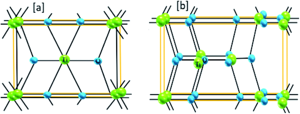 | ||
| Fig. 2 The bulk crystalline structures of (a) rutile-phase and (b) anatase-phase materials; green: titanium, blue: oxygen (this figure has been redrawn from ref. 4). | ||
Sensor parameters and associated devices
The general correlation between sensor parameters has been investigated in a qualitative as well as quantitative manner. The performances of oxide-based sensors are governed by the morphologies and structures of the sensing materials. For example, adjusting the particle size of the sensing material or doping with foreign elements can result in a great improvement in the sensor response. Based on the “small size effect” phenomenon, the response (S) increases when the particle size (d) of the material is approximately double the thickness of the space-charge layer (w).29 Nanomaterials offers a greater surface to volume ratio (SVR) depending on the dimensions of the nanostructures. A higher SVR leads to more adsorption sites, facilitating a higher sensor response (S). On the other hand, the thickness of the grown film (t) or the particle size (d) is inversely proportional to the sensitivity (S). This relationship (S ∝ 1/d) can lead to a faster response time.23 In addition, the temperature has a significant influence on the sensor response time and reversibility. A higher operating temperature drastically speeds up the response time and improves the reversible characteristics of a sensor. However, a higher operating temperature sometimes limits maximum detection owing to the tendency of adsorbed molecules to saturate on the surfaces.4 The problem of the need for high operating temperatures can be easily resolved through the modification of structural parameters like crystal shape and orientation.4 The manipulation of materials on the nanoscale with reactive crystal facets can be an alternative approach for reducing operating temperatures and, hence, supporting low power consumption.4 The effects of pore size on sensitivity have been explored by many researchers.22 Porous sensing materials can offer enhanced sensitivity in a linear fashion.23 However, the pore size does not always maintain a linear relationship with sensitivity. Furthermore, the response/recovery rates become faster in materials with numerous pores. In a porous material, the gas diffusion mechanism solely depends on the size of the pores and the gas diffusion constant.7 Based on the Knudsen diffusion process, the diffusion constant (DK) can be empirically related to the pore radius (r), temperature (T), molecular weight (M), and gas constant (R) based on the relationship .7 The diffusion constant proportionally varies with the pore radius, which can lead to higher sensitivity. As far as crystallinity is concerned, materials with smaller crystallites exhibit greater sensitivity though an increase in the depletion layer width (w).7 The depletion layer width (w) is related to the sensor response as follows: S = (Δn/n) × w, where n is the charge carrier (e/h) concentration and Δn is the difference in charge carrier concentration in air and after gas exposure. The depletion layer width (w) can be further correlated with temperature as follows: w = (εokT/ne2)0.5, where ε0 is the dielectric constant of the material, k is the Boltzmann constant, and T is temperature.19
Sensing mechanisms
The working principle of a gas sensor is based on changes in the electrical conductivity of the sensing material. Due to the enormous number of surface sites, most target gas molecules are adsorbed by oxygen ions that have been already adsorbed at the metal-oxide surface. Interactions between the adsorbed target species and the oxygen ions can modulate the charge carrier concentration and hence change the conductivity (or resistivity) of the material. Table 1 shows a summary of the conductivity changes of n-type and p-type materials upon exposure to reducing and oxidizing gases.| Material property | n-Type | p-Type | Type of gas |
|---|---|---|---|
| Conductivity | Increases | Decreases | Reducing |
| Carrier concentration | Increases | Decreases | |
| Conductivity | Decreases | Increases | Oxidizing |
| Carrier concentration | Decreases | Increases |
Generally, physisorption and chemisorption are the two processes that take place at the sensing layer, depending on temperature variations. Physisorption is an exothermic reaction that occurs at low temperature and chemisorption is an endothermic reaction that occurs at higher temperatures.2 In general, the physisorption of adsorbed O2 and its subsequent transformation to O−2 happen at lower operating temperatures (<100 °C).2,19 On the other hand, at relatively higher temperatures (>100 °C), physisorbed oxygen species are transformed into chemisorbed O−, which is more stable and reactive to different types of gases.40–42 Therefore, temperature has a significant role in this mechanism, as it ensures the formation of different oxygen species (as shown in eqn (1)–(3)).
| O2(gas) ↔ O2(ads) | (1) |
| O2(ads) + e− = O2−[<100 °C] | (2) |
| O2(ads)− + e− = 2O(ads)−[100–300 °C] | (3) |
The width of the depletion layer during the aforementioned phenomenon is found to be at a maximum provided the oxide semiconductor is n-type. However, the width of the depletion layer might be modulated depending on the type of target species that interacts with the oxygen species.41 For example, an n-type sensing material exposed to oxidizing gases (NO, NO2, Cl2, and O3) results in a depletion layer with a larger width compared to the case when only oxygen was adsorbed on the sensing surface.23,41 Such gas-dependent depletion layer thickness variations lead to modulations of electron concentrations, eventually changing the resistance of the sensing material.
The role of junction effects
For a better understanding of sensing phenomena, a SnO2 nanowire model exposed to an oxidizing gas (NO2) has been taken under consideration (as shown in Fig. 3(a) and (b)).40 Under ambient conditions, the electron-donating capabilities of SnO2 depend on the state of the oxygen vacancies (VO), which is largely governed by the secondary ionization energy.8 The release of electrons and a subsequent change to a +1 ionic valence state lead to a change in the depletion width (w).8 Upon the exposure to NO2 (an oxidizing gas) of the nanowire junctions, two ionic states below the edge of the conduction band are formed.8 Such ionic states cause the depletion layer to increase in width and, hence, undergo band bending, compared to in the case of air exposure alone. These junctions correspond to active points where electrons from the conduction band of the semiconductor are transferred to the adsorbed NO2 (acting as an electron acceptor), leading to the formation of a depletion layer near the junction and an increase in the potential barrier (as shown in Fig. 3(b)). A comparison between single nanowire devices (where only a single nanowire lies between two electrodes) and a multi-nanowire network reveals a more effective sensor response in the case of the latter due to the adsorption effects of multiple junctions.40 To the contrary, a single nanowire device offers a fast response towards the target species, possibly attributed to the idea that electrons have almost no barrier (except the ohmic junction at the electrode-semiconductor interface) to overcome, whereas there are multiple barriers (formed between many nanowires) in the multi-nanowire network. Electron transport in the semiconductor is affected by the height of the potential barrier (Ψb). A potential barrier in micro/nano sensor devices may form either at the junction between two grains, at the electrode–semiconductor interface, or at both interfaces. However, the barrier height at the electrode-semiconductor (sensing material) interface (ΨMS) plays a significant role in determining the gas sensor performance. The electron flow does not face much of an obstacle to overcome the low barrier height at the ohmic junction (which forms at the electrode–semiconductor interface). However, in the case of Schottky contact, the barrier height (ΨMS) is related to the electron affinity (χ) and work function of the metal (Φm) as follows: ΨMS = Φm − χ.7,8,40 The effects of the Schottky barrier interface between single wall carbon nanotubes (SWCNTs) and ZnO (χ = 4.35 eV) have been investigated by Kim et al.8 The authors suggest that the improved NO2 sensing performance can be attributed to the formation of a lower Schottky barrier height of ∼0.67 eV with the use of SWCNTs as electrodes (Φm = 5.02 eV).8 Electrode variations also have an influence on sensor parameters, which may be explained via employing a thermionic emission model to analyze the Schottky barrier height. Different electrodes, such as Au and Pd, have been studied to measure the differences in sensor response.8 Obviously, work function differences between the two material will create a barrier height as follows: Ψb = ΨMS = Φm − Φs = (kBT/e) × ln(Im/IS), where Φs is the work function of the semiconductor, kB is the Boltzmann constant, Im is the current running through the metal, and IS is the current running through the semiconductor. Therefore, based on the barrier height model, one can easily calculate the sensor response following the equation:19 | (4) |
 | ||
| Fig. 3 (a) A schematic diagram showing a model of SnO2 nanowires connected between two electrodes. (b) An enlarged view of nanojunction formation and a corresponding energy band diagram (this figure has been reproduced from ref. 40 with permission from IOP Publishing Ltd, copyright 2008). (c) CAFM current mapping of an oxide/graphene composite with a scanning area of 500 nm × 250 nm. (d) The XPS study of pristine graphene, an oxide/graphene composite, and an oxide material, and (e) the current voltage characteristics from the junction study (this figure has been reproduced from ref. 7 with permission from the Royal Society Of Chemistry, copyright 2015). | ||
Carrier transportation through the geometry of a SnO2/graphene junction has been studied using conductive atomic force microscopy (CAFM) (as shown in Fig. 3(c)).7 One can understand the barrier height concept in the SnO2/graphene junction by looking at Fig. 3(c) (the left side reveals an AFM image of the SnO2/graphene surface, whereas the right side demonstrates the conductivity differences on the surface). The highlighted black circles represent void regions on the surface, which facilitate the flow of a larger amount of majority carriers (larger current), reflecting the existence of a smaller barrier height. Currents through the junction were measured at different bias voltages in CAFM mode for pristine graphene, SnO2/graphene, NiO/graphene, and CuO/graphene (as shown in Fig. 3(e)). Fig. 3(e) suggests that a maximum current was recorded for the junction having the lowest barrier height. In this regard, SnO2/graphene offered the lowest barrier height, as it has the maximum flow of carriers out of all the samples at the same bias voltage. Differences in barrier height can be confirmed through valance band spectra studies.7 Valence band spectra from XPS data provide the electronic states near the Fermi level. For example, the differences between the valence band maximum and the Fermi level before and after SnO2 deposition on graphene were found to be 3.2 eV and 3.4 eV, respectively (as shown in Fig. 3(d)). Therefore, electrons can pass through the SnO2/graphene barrier height of 0.2 eV efficiently.
Zhang et al. investigated the performance of an acetone gas sensor made of heterostructured n-type SnO2 with p-type reduced graphene oxide.43 The gas interacts at the junction (the depletion layer), where acetone acts as an electron donor, thereby increasing the carrying of negative charge to the n-type thin-film. When acetone is absorbed, gas molecules cause a change in the hole concentration of RGO. As a result, the resistance of the sensor decreases. As far as the doping or addition of foreign elements is concerned, additional adsorption sites increase the sensor response drastically.
LUMO energy
The temperature-dependent gas sensing mechanism towards different gases (selectivity) can be further understood based on the concept of the lowest unoccupied molecular orbital (LUMO) energy model. The sensing of a particular gas can be related to the LUMO energy of the gas atom and the amount of gas adsorption on the sensing material at various working temperatures.44 For example, a study by Wen et al.44 suggested that the orbital energies of ethanol, methanol, acetone, and formaldehyde were found to be 0.12572 eV, 0.19728 eV, 0.20525 eV, and 0.21965 eV, respectively. Lower-LUMO-energy molecules can be detected at lower temperatures.44 The study revealed that ethanol has the lowest LUMO energy (∼0.12572 eV) and offers a maximum response at 280 °C. On the other hand, the molecules with higher LUMO energies (methanol, acetone, and formaldehyde) require higher operating temperatures (from 320–362 °C) to achieve a maximum response. This is possibly due to the inverse relationship between the electron transfer capabilities and the LUMO energy.The role of defect states
The gas sensor response depends on the donor or acceptor type, semiconductor surface states, surface defects, native point defects, etc.45 The relationship between the sensor response and defect states has been analyzed here considering a ZnO donor surface as a case study. Six types of defects are dominant in ZnO: zinc anti-sites (ZnO), zinc interstitials (Zni), zinc vacancies (VZn), oxygen anti-sites (OZn), oxygen interstitials (Oi), and oxygen vacancies (VO).45 Owing to their higher formation energy, zinc anti-sites (ZnO) are generally not found on the ZnO surface, whereas the relatively lower formation energies ensure an abundance of zinc interstitials (Zni) and oxygen vacancies (VO). These defects (Zni and VO) act as donors and offer electrons in the ZnO crystal structure. To the contrary, remaining defects, like zinc vacancies (VTi), oxygen interstitials (Oi), and oxygen anti-sites (OTi), accept free electrons and act as acceptors.45 The electron accepting and donating mechanisms are shown in eqn (5) and (6). | (5) |
 | (6) |
Oxygen adsorption and its transformation to O− upon accepting one electron occur at the active sites of zinc interstitials (Zni) and oxygen vacancies (VO) near the surface. These active sites act as oxidation centres for the target gas molecules. On the other hand, OZn and Oi reduce the formation of O− species via accepting electrons and create an opposing effect during chemisorption compared to Zni and VO.37 Therefore, it can be stated that only specific defects having electron donation capabilities can enhance the sensor response dramatically. Generally, the sensor response initially increases at a faster rate and then the response rate decreases, gradually tending to a saturation level. Such a phenomenon can possibly be explained as follows: initial molecular adsorption at relatively lower energy binding sites expedites surface adsorption at a faster pace, resulting in a faster response, whereas the slow response is ascribed to the saturation of surface sites, with molecular interactions only occurring at the higher energy binding sites, viz., defects, vacancies, and oxygen functional groups.46 In addition, the greater the availability of high-energy binding sites at the sensing surface, the better the sensor recovery characteristics.
The role of humidity
It is essential to specify up to what percentage (%) level of humidity the sensor response remains invariable in a commercial sensor datasheet. Almost every micro/nano sensor possesses response variations in the presence of different levels of humidity. Therefore, in this section, humidity sensing mechanisms based on a proton (H+) hopping model (as shown in Fig. 4) are discussed.20 Water molecules on the sensing surface dissociate to form H+ and OH−. Dipole OH− ions adsorb on the sensing surface and make bonds with the semiconductor grains. For a better understanding, we have considered TiO2 as the semiconductor surface here. Mainly, dipole OH− ions bonded with titanium interstitials, TiTi, and formed water dipoles in the form of (Tiδ+Ti– OHδ−), as shown in eqn (7) and (8). The bonding of OH groups with TiO2 grain sites is shown pictorially in Fig. 4. On the other hand, H+ ions (protons) hop from one grain to another through the temporary formation of hydronium ions (H3O+). Along the hopping path, ions (protons) may react with either adsorbed oxygen species (O−) or lattice oxygen (OO) based on the availability on the surface. Bonding between H+ and O− produces neutral hydroxyl ions (OH) and many of these hydroxyls (OH) form water vapor, which is purged from the surface. To the contrary, the reaction of H+ with lattice oxygen (OO) offers either rooted (OH+rooted) or oxygen (V++O) vacancies via releasing electrons (as shown in eqn (7) and (8)). The process of water molecule adsorption can lead to H+ transfer, which can not only change the electrical resistance but also the refractive index. The change in this latter property can be used to detect water vapor in the range between 10% and 90% relative humidity.| TiTi + (H+–OH−)ads + OO = [TiTiδ+–OHδ−] + OH+rooted + e− | (7) |
| 2TiTi + (H+–OH−)ads + OO = 2[TiTiδ+–OHδ−] + V++O + 2e− | (8) |
 | ||
| Fig. 4 Inter- and intra-grain proton-hopping model. | ||
Influence of the sensor structure
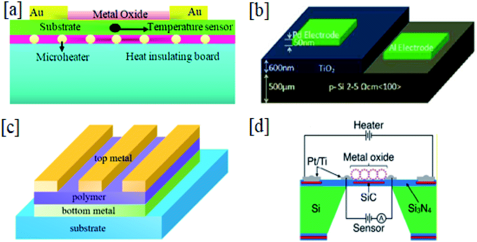 | ||
| Fig. 5 Schematic diagrams of (a) a thin-film resistive gas sensor (this figure has been reproduced from ref. 47 with permission from Elsevier, copyright 2003), (b) a metal–insulator–semiconductor (MIS) structure, (c) a metal–insulator–metal (MIM) structure, and (d) a sensor with microheater integration (this figure has been reproduced from ref. 50 with permission from ACS Publications, copyright 2017). | ||
 | ||
| Fig. 6 (a) A schematic view of a CCFET gas sensor (this figure has been reproduced from ref. 66 with permission from Elsevier, copyright 1996). (b) Optical images of a metal-oxide/graphene composite transistor. (c) The AFM surface morphology of SnO2/graphene. (d) The drain current as a function of the gate voltage from graphene composites with SnO2, CuO, and ZnO, and (e) the gas-sensing characteristics of an oxide–graphene composite transistor (this figure has been reproduced from ref. 7 with permission from the Royal Society of Chemistry, copyright 2015). | ||
The influence of the sensor structure on the gas-sensing performance is tabulated in Table 2. Cerium oxide (CeO2) porous thick film with a particle size of 100 nm was investigated for oxygen-gas sensing. The sensor showed a fast response within <8 s at 615 °C.51,52 It is possible that the existence of channels as well as surface accessibility for target gas molecules and subsequent adsorption/desorption, facilitated by the hierarchical porous structure, are the reasons for the excellent sensing performance compared to bulk or solid materials. Basu et al. reported porous ZnO-thin-film-based Pd–Ag/ZnO/Zn and Rh/ZnO/Zn MIM (metal–insulator–metal) methane sensors.67 The results revealed that Pd–Ag/ZnO/Zn offers fast response and recovery times for the detection of 1% methane.67 The influence of pre-biasing techniques on indium–gallium–zinc oxide (IGZO) TFT devices for NO2 sensing were studied by Park et al.65 It was observed that the sensing performance improved when the temperature was increased to 90 °C, which could possibly be attributed to the effect of the electric-field-induced chemisorption of NO2 in the channels of the IGZO TFT.65 Most TFT-based sensors face the problem of baseline recovery (the return to baseline resistance before gas exposure). The recovery rate of TFT-based sensors can be improved via irradiation with UV light at the sensing channel.60 UV light irradiation results in the removal of oxygen ions from the sensing surface and ensures fewer interactions with gas molecules. It was observed that only a few gas molecules remain in the vicinity of the sensing surface, as such irradiation yields faster removal rates of gas molecules.68 Furthermore, interdigital capacitive (IDC) structures coated with a cobalt ferrite (CoFe2O4) nanocomposite have been employed for ethanol gas sensing. The device showed a near-room-temperature (31 °C) ethanol response, even at a concentration of 7 ppm, with a response time of 180 s.69
| No. | Structure | Material | Opt temp. (°C) | D. range (ppm) | Res. time (s) | Rec. time (s) | Gas | Stability | Ref. |
|---|---|---|---|---|---|---|---|---|---|
| a Opt temp. = optimum temperature. b D. range = dynamic range. c Res. time = response time. d Rec. time = recovery time. e Ref. = reference, NA = not applicable. | |||||||||
| 1 | Resistive | Cerium oxide | 700 | 105–103 Pa | 10 | NA | O2 | Good | 52 |
| Cerium oxide | 615 | 0.01–1 Pa | 11 | 8 | O2 | Excellent | 53 | ||
| p-TiO2 | 320 | 50 | 120 | <60 | Ethanol | Average | 21 | ||
| Carbon nanotubes | 25 | 0.48–2.34% | 90 | 140 | Acetone | Average | 53 | ||
| 2 | MIS | Pd–SiO2–Si | 667 | 200 | 20 | 40 | F144 | Poor | 54 |
| Pd–TiO2–Si | 200 | 0.5–50 | 7 | 20 | Acetone | Good | 48 | ||
| Pd–Si3N4–SiO2–Si | 150 | 500 | 50 | 150 | H2 | Poor | 55 | ||
| Pd–TiO2 thin film | 50 | 0.1–2 | 10 | 120 | H2 | Poor | 34 | ||
| Pd–Ag/PS/Si/Al | 27 | 0.01–1% | 8 | 207 | H2 | High | 56 | ||
| 3 | MIM | Rh/ZnO/Zn | 220 | 0.01–1% | 24.5 | 72.3 | CH4 | Good | 67 |
| Pd–Ag/ZnO/Zn | 220 | 0.01–1% | 5.1 | 16.14 | CH4 | Good | 67 | ||
| Pd/ZnO/Zn | 27 | 2000–20![[thin space (1/6-em)]](https://www.rsc.org/images/entities/char_2009.gif) 000 000 |
120 | 840 | H2 | Poor | 58 | ||
| Pd–Ag/ZnO/Zn | 150–300 | 0.01–1% | 5.1 | 16.1 | CH4 | Good | 57 | ||
| TiO2 | 23 | 10–90% | 25 | 65 | H2O | Satisfactory | 49 | ||
| 4 | TFT | InGaZnO | 90 | 1–20 | 20 | NA | NO2 | NA | 65 |
| WS2/IGZO | 27 | 1–300 | NA | 30 min | NO2 | Average | 62 | ||
| Pentacene | 27 | 0.5–3 | 70 | 60 | NH3 | Poor | 63 | ||
| 5 | Capacitive | CoFe2O4 | 31 | 7–100 | 180 | 180 | Ethanol | NA | 69 |
| Graphene oxide | 25 | 1–70 | 20 | 15 | Ethanol | Excellent | 70 | ||
| Al2O3 | NA | 40–98% | 10–90 | NA | H2O | NA | 71 | ||
Alcohol sensors
The efficient detection of the vapor phases of a wide range of organic molecules, including alcohols, ketones and aromatic hydrocarbons, by means of metal-oxide nanostructure is an extremely important area as far as pollution control is concerned.70–103 Alcohol consumption can cause driving errors together with traffic-rule violations, potentially leading to death. The inhalation of alcohol may lead to headaches, queasiness, stomach pains, vertigo, nausea, sluggishness, eye irritation, and cerebral pain.70–85 Therefore, alcohol detection is in high demand to prevent dangerous driving and for food quality monitoring, especially alcoholic beverages.State-of-the-art alcohol, ketone, and BTX sensing studies are tabulated in Table 3. A comparative study of pure and Au-modified ZnO nanowires for ethanol sensing was carried out by Ramgir et al.72 The results show that the Au-modified sensor films have faster response/recovery times: 5 s and 20 s, respectively. These faster reaction kinetics are attributed to the catalytic activity of Au, as well as nano-Schottky Au–ZnO junction formation.72 The surface engineering of TiO2 nanobelts via photoreduction through an acid-corrosion procedure for the formation of Ag–TiO2 heterostructures offered higher sensitivity and selectivity towards ethanol with improved response times. It is believed that the manipulation of the surface roughness and the metal–TiO2 composite heterostructures were the influencing factors determining the chemical sensitization dynamics based on interfacial charge transfer.33 The role of porous nanostructures in determining ethanol sensing behaviour was investigated by Yang et al.73 SnO2/Zn2SnO4 hierarchical porous nanospheres were found to offer an optimum response at 250 °C, with a detection limit as low as 0.5 ppm. The lower detection limit of the SnO2/Zn2SnO4 nanospheres can possibly be attributed to the porous structure, as well as heterojunction formation between SnO2 and Zn2SnO4.73 A room-temperature ethanol study was carried out by Pandeeswari et al.82 and Shao et al.74 As per Shao et al., synergistic effects from the heterojunctions (Au/SnO2 and C60/SnO2) and the modulation of potential barriers play crucial roles in enhancing the detection performance.74
| No. | Material | Material synthesis | Vapor | Opt. temp. | D. range (ppm) | RM (%) | Res. time (s) | Rec. time (s) | Ref. |
|---|---|---|---|---|---|---|---|---|---|
| a Opt temp. = optimum temperature. b D. range = dynamic range. c RM = response magnitude. d Res. time = response time. e Rec. time = recovery time. f Ref = reference, E = ethanol, M = methanol, P = 2-propanol, B = benzene, T = toluene, X = xylene, K = ketone. | |||||||||
| 1 | ZnO nanowires | Hydrothermal | E | 325 | 5–100 | 1.33 | 5 | 20 | 72 |
| 2 | SnO2 nanorods | Hydrothermal | E | 300 | 10–300 | 31.4 | 1 | 1 | 77 |
| 3 | Aloe-like SnO2 | Hydrothermal | E | 285 | 50–1000 ppb | 23 | 1.53 | 76 | 78 |
| 4 | ZnO nanorods | Hydrothermal | E | 280 | 12.5–500 | 2.5 | 16 | 120 | 79 |
| 5 | TiO2 nanobelts | Hydrothermal | E | 250 | 20–500 | 33.661 | 1 | 2 | 33 |
| 6 | Zn2SnO4 spheres | Hydrothermal | E | 250 | 0.5–100 | 1.4 | 2 | 114 | 73 |
| 7 | Er-doped SnO2 | Co-precipitation | E | 240 | 20–750 | 48 | 35 | 40 | 80 |
| 8 | CuO nanocrystals | RF sputtering | E | 180 | 12.5–500 | 2.2 | 31 | 52 | 81 |
| 9 | TiO2 thin film | Sol–gel dip | E | 30 | 10–50 | 14–535 | 65 | 20 | 82 |
| 10 | Au–SnO2/C60 | Hydrothermal | E | 27 | 0.5–50 | 16.8 | 35 | 9 | 74 |
| 11 | SnO2 thin film | Sol–gel | M | 350 | 2600–100000 |
24 | NA | NA | 61 |
| 12 | Al-doped NiO | Facile method | M | 325 | 10–500 | 10.4 | 199 | 15 | 28 |
| 13 | Ce-doped In2O3 | Hydrothermal | M | 320 | 35.2–100 | 35.2 | 14 | 10 | 24 |
| 14 | InWO3 | Hydrothermal | M | 312 | 20–1000 | 18.1 | 2 | 9 | 75 |
| 15 | α-Fe2O3 spheres | Hydrothermal | M | 280 | 1–100 | 25.1 | 8 | 9 | 76 |
| 16 | ZnO/SnO2 | Hydrothermal | M | 200 | 1–300 | 80 | 20 | 65 | 83 |
| 17 | La1−xMgxFeO3 | Template method | M | 190 | 10–300 | 146.2 | 17.7 | 25.4 | 84 |
| 18 | SnO2 spheres | Solvothermal | M | 80 | 5–500 | 190.88 | 10 | 10 | 85 |
| 19 | TeO2 nanowires | Evaporation | P | 50 | 100–1000 | 3.15 | <30 | <30 | 86 |
| 20 | Hollow CuO fibers | Template method | P | 200 | 1–100 | 4.66 | 19.18 | 63 | 87 |
| 21 | ZnSnO3 | Facile precipitation | P | 200 | 1–500 | 10.3 | <100 | 90 | 88 |
| 22 | SmFeO3 powders | Decomposition | P | 400 | 0.01–3 | 11 | 0.5 | 3 | 89 |
| 23 | Ag/SnO2 spheres | Chemical route | P | 300 | 50–300 | 146.02 | 20 | 150 | 90 |
| 24 | SrCO3/graphene | Cataluminescence | P | 245 | 0.2–32 | 5.8 | 2 | 20 | 91 |
| 25 | TiO2 thick film | Chemical method | P | 120 | 0–5000 | 60 | NA | NA | 92 |
| 26 | Au-α-MoO3 hollow spheres | Solvothermal | B | 250 | 5–100 | 1.3 | NA | NA | 96 |
| T | 0.1–100 | 2.5 | 11 | 57 | |||||
| X | 0.5–100 | 5.1 | 118 | 289 | |||||
| 27 | Cu2O octahedra | Vapor deposition | B | 230 | 5–200 | 4.3 | 3 | 4 | 93 |
| 28 | Au–ZnO | Hydrothermal | B | 206 | 1–200 | 16.25 | 5 | 36 | 97 |
| T | 46.43 | 2 | 50 | ||||||
| X | 76.47 | 2 | 24 | ||||||
| 29 | ZnO nanoflower | CBD | B | 200 | 0.5–700 | 79.1 | 15 | 58 | 98 |
| T | 85.4 | 10 | 50 | ||||||
| X | 87.4 | 9 | 38 | ||||||
| 30 | TiO2 nanotubes | Anodization | B | 150 | 1–400 | 25 | 56.14 | 152.96 | 35 |
| T | 21 | 84.93 | 128.54 | ||||||
| X | 20 | 103.80 | 152.30 | ||||||
| 31 | Carbon nanotubes | Dispersion | T | 27 | 400–1200 | 0.001 | 120 | 8 | 99 |
| 32 | Carbon nanotubes | Chemical method | B | 25 | 33–500 | 0.7 | 1.5 | 2.75 | 100 |
| T | 1 | 2.5 | 1.75 | ||||||
| X | 5 | 6 | 4 | ||||||
| 33 | SnO2 reduced graphene oxide | Facile hydrothermal | K | 27 | 10–2000 | 2.19–9.72 | 300 | 200 | 43 |
| 34 | ZnO nanorods | Aqueous solution | K | 300 | 1–100 | 30.4 | 5 | 15 | 95 |
| 35 | ZnFe2O4 nanospheres | Solvothermal | K | 200 | 11.8–30 | 42.1 | 9 | 272 | 25 |
| 36 | ZnO thin film | CVD | K | 250–375 | 1000–2000 | 45 | 240 | 250 | 101 |
| 37 | ZnO–SnO2 nanowires | CVD | K | 140–320 | 0.01–0.2 | NA | 7 | 40 | 94 |
| 38 | PdAu/SnO2 nanosheets | Hydro-solvothermal | K | 250 | 1–100 | 6.5 | 5 | 4 | 102 |
| 39 | Co3O4 nanocubes | One-pot hydrothermal | K | 240 | 10–1000 | 4.88 | 2 | 5 | 103 |
The facile synthesis of 3 mol% Al-doped NiO nanofibers resulted in a significant increase in methanol response at temperatures from 225 °C to the optimal operating temperature, and the limit of detection became lower as the temperature was increased further.35 Composites of indium tungsten oxide with different In/W ratios exhibited an ultrafast response to methanol at an optimum temperature of 312 °C. The fastest response time of 2 s and recovery time of 9 s were recorded at a methanol concentration of 200 ppm.35 The fast response/recovery characteristics are possibly due to the enhanced surface states in the device channels due to majority carrier accumulation around the fully charged grain boundary sites. Three-dimensional effects from nanostructures possibly offer better sensing properties, as was observed in the work of Yang et al.76 In their research, a hematite (α-Fe2O3) hollow sphere based sensor offered a low methanol detection limit of 1 ppm and optimal sensing performance at 280 °C.76 3D nanostructures with numerous macro/micropores can be an additional advantage in gas sensing. La1−xMgxFeO3 3D macroporous structures with different concentrations of Mg2+ doping reduced the optimum operating temperature to 190 °C, with very good selectivity towards methanol. Possibly, the ordered macro/micropores in the material together with Mg2+ doping make this sensor more sensitive and selective towards methanol.84
Thermally synthesized single-crystal tetragonal TeO2 nanowires with a very high surface-to-volume ratio showed 2-propanol detection at 50 °C.86 The increasing response magnitude trend at lower temperatures is possibly due to a surface-limited reaction mechanism in this temperature range, whereas above a certain temperature (or at higher temperatures), a decreasing trend was found due to a concomitant process involving a decrease in chemisorbed oxygen ions and mass transfer limitations compared to the fast reaction kinetics.50 Employing cotton fibres as a bio-template in combination with facile solution combustion resulted in hollow CuO fibres with lengths in the micrometer range, which exhibited excellent sensitivity and reproducibility, and good selectivity toward 2-propanolin at concentrations ranging from 1–100 ppm.87 The catalytic effect of Ag nanoparticles on SnO2 hollow spheres played an important role in determining sensor stability and selectivity.90 A metal-oxide and graphene composite (SrCO3/graphene) exhibited a 2-propanol response 5.8 times higher than that of pure SrCO3.91
Benzene, toluene and xylene (BTX) sensors
The aromatic hydrocarbons benzene, toluene, and xylene (BTX) have a carcinogenic nature, and they are by-products in many petrochemical industries, including coal processing and oil refining.97 BTX easily mixes with air through vehicle exhaust, makeup, glue, and paint emission.35 Breathing a small amount of BTX may cause abnormalities in the nervous system, leukemia, lymphoma, and blood production issues.98 Further, monitoring BTX emitted by fruits like oranges in various stages of ripeness can help harvesting to be carried out in good time before spoilage.35 Template-free solvothermally synthesized hierarchical α-MoO3 hollow spheres were modified with different amounts of Au nanoparticles to form hybrid nanomaterials for improving the BTX response.97 The optimum response was found to be significantly higher in Au-loaded α-MoO3 than in pristine α-MoO3.96 Very fast benzene sensing (∼3 s), employing novel concave Cu2O octahedral nanostructures, has been reported by Wang et al.93 The fast response and recovery times were attributed to the surface area, pore size, and transport mechanism. The surface area of the concave Cu2O octahedra was as high as 18.9 m2 g−1. Furthermore, gaps of ca. 9 nm between cross-linked nanoparticles possibly facilitate the generation of more active sites for benzene sensing. Electrochemically synthesized titanium dioxide (TiO2) nanotubes offered BTX sensing at a relatively low temperature of around 150 °C. Studies reveal that benzene generated the highest response, followed by toluene and xylene.2,8 In particular, for BTX sensing, a high temperature is the prime requirement due to the high-energy bond-breaking. However, near-room-temperature sensing has been observed using some non-metal oxide materials.99,100 Two such works are included for better comparison.Ketone sensors
Ketones find widespread applications in pharmaceuticals, nail polish remover, and paints, and they are used as solvents for many complex organic compounds. A room-temperature acetone sensing study, utilizing hybrid SnO2-reduced graphene oxide thin film, in the concentration range of 10–2000 ppm has been reported by Zhang et al.43 The acetone response was found to be two-times higher than that of pure RGO, which can possibly be attributed to the higher surface area of the 3D porous nanostructure of the RGO sheets and SnO2 nanoparticles. A sensor with interdigitated electrodes utilizing single crystal hexagonal ZnO nanorods deposited on a Si wafer offered promising acetone sensing performance at 300 °C, with response and recovery times of ∼5 s and 15 s, respectively.95 Such Si-technology-based sensors have flexibility for large-scale production at low cost. A template-free solvothermal route with ethanol/ethylene glycol (EG) as binary solvents was employed to prepare porous ZnFe2O4 spherical structures.25 The fabricated sensor offered excellent selectivity toward acetone at an optimum temperature of 200 °C, with a response magnitude of ∼11.8. A cataluminescence ketone sensor employing a composite form of SnO2:ZnO nanowires coated with Au/reduced-graphene-oxide was developed by Yu et al.94 Their sensor showed an extremely low acetone detection limit down to 0.01 ppm acetone at 140 °C. The possibly catalytic effect of the Au (∼14 nm in size)/reduced graphene oxide composite gives this sensor a fast response with excellent repeatability.94
Effects of nanostructure dimensionality
The nanostructure dimension affects the gas sensing performance drastically. Zero-dimensional nanoparticles offer higher numbers of adsorption sites and better catalytic activity, possibly lowering the activation energy required for gas-molecule dissociation.6,7,18 Smaller particles (<10 nm) accumulate more majority carriers in the sensing channels than bigger particles.2 Furthermore, a particle size of <10 nm or less than the width of depletion region (w) ensures depletion region overlap, which leads to flat band condition. Under these conditions, no potential barrier is found between the surface and bulk material and the sensitivity is enhanced greatly, as the surface state is dominant. However, the use of such small-sized particles is limited by thermal instability, agglomeration, and film porosity.2,41 One-dimensional materials, such as nanowires, nanorods, nanoribbons, and nanotubes, offer higher sensitivity compared to conventional materials, such as bulk materials or thin films, under a wide variety of operating conditions. All these nanostructures have radii of 10–100 nm, which are comparable to the width of the depletion region (w), facilitating the easy modulation of the conduction channels.22 A high surface-to-volume ratio, good surface accessibility, and chemical/thermal stability are possibly the reasons for the better transport qualities. Hollow nanostructures, such as nanocages and nanospheres, are excellent gas-sensing materials, facilitating high permeability with an optimal surface area for gas diffusion. Optimal sensing at the active surface sites results in higher sensitivity with optimum response/recovery characteristics.Nanostructures with hollow structures are achieved through controlled synthesis, such as layer-by-layer coating, template-free hydrothermal self-assembly, and sacrificial template methods (chemical precipitation or spray pyrolysis).50 So many techniques, including chemical processes and physical processes, are available to grow off-chip nanostructures. In general, off-chip nanomaterials are first synthesized and then transformed on the heating platform for integration. Integration is done either via drop-casting or spin-coating methods. However, such transformations of nanomaterials on the heater may severely affect the intended morphology, reduce the heating area, lead to a loss of sensing surface, or result in poor electrode bonding with the sensing surface.50 However, on-chip nanomaterial production on integrated platforms can become complex and necessitates the development of sophisticated techniques to control the growth direction, which possibly leads to better morphology control. Most researchers have employed colloidal spheres as sacrificial templates or carried out the capillary infiltration of a liquid precursor to fabricate hollow spheres or macropores in metal oxide structures, respectively, due to the ease of self-assembly and the high mechanical stability.50 Such 3D hollow spheres offer three-dimensional interactions with the analysis gases, facilitating rapid sensing with short recovery times via maintaining equilibrium between the surface reactions and rates of reactant diffusion.
As far as gas sensing is concerned, key features of nanostructures are as follows. (i) Nanoparticles offer higher surface-to-volume ratios, which facilitate a maximum number of interaction sites compared with nanomaterials with different dimensionality. (ii) One-dimensional electron transport through a minimum number of grain boundaries improves the response/recovery characteristics of sensor devices. (iii) Two-dimensional (2D) nanostructures offer free edge energy to the system, which eventually increases the activation energy for gas adsorption and desorption. (iv) Three-dimensional (3D) nanostructures offer a larger surface area, as well as free surface energy.20,21,41,45Table 4 shows the nanostructure dimensionality effects on sensor performance. Sol–gel-derived ZnO nanoparticles showed fast response (2 s) and recovery (20 s) times at 280 °C for NO2 sensing.18 A sensor made of spray-pyrolysis-synthesized ZnO nanocrystals on carbon nanotubes (ZnO-CNT) showed linear sensitivity towards methanol gas at 200 °C.115 Temperature-controlled conductivity and transconductance plays a significant role in the use of this active ZnO-CNT material for sensing gas.115 Al-doped ZnO ultrathin nanosheets exposed to ethanol offered a response magnitude of 90.2 with a response time/recovery time of 1.6 s/1.8 s at 370 °C. Furthermore, the sensor exhibits a highly repeatable nature, and it is ethanol-selective with long-term stability.12 Doping-induced intrinsic defects as well as surface energy of the exposed nanosheet planes are possibly the reasons for the excellent sensing properties towards ethanol.12 The chemical vapor deposition (CVD) of a single SnO2 nanowire between two metal electrodes has been investigated for ethanol detection.124 A single nanowire (diameter: 60 nm; length: 3.5 μm) is capable of selectively detecting seven different gases with 94.3% accuracy based on principal component analysis and a machine learning algorithm.124 The performance of Pd-loaded SnO2 hollow spheres (obtained via an adsorption–calcination process) towards methane showed a response magnitude of 4.88 at 300 °C, with a fast response time/recovery time of 3 s/7 s.129 Oxygen spillover due to the catalytic effects of Pd and PdO–SnO2 heterostructures result in better CH4 sensing performance compared to pristine SnO2.129
| No. | Structure | Material | Method | Temp. (°C) | Conc. (ppm) | Gas | Res. time (s) | Rec. time (s) | Ref. |
|---|---|---|---|---|---|---|---|---|---|
| a Temp. = optimum temperature. b Conc. = concentration. c Res. time = response time. d Rec. time = recovery time. e Ref = reference, NA = not available. | |||||||||
| 1 | Nanoparticles | ZnO | Brush coating | 280 | 234 | NO2 | 2 | 20 | 18 |
| ZIF-67 SnO2 nanoparticles | Chemical | 205 | 5000 | CO2 | 15 | 25 | 104 | ||
| Cd2SnO4 nanoparticles | Combustion | 170 | Alcohol | 14 | 280 | 6 | |||
| RGO-decorated ZnO | RF sputtering | 150 | 100 | H2 | 28 | NA | 105 | ||
| Graphene and SnO2 | CVD | 50 | 100 | H2 | 1 | 1 | 7 | ||
| Carbon nanoparticles | Chemical | 27 | 100 | CO and H2 | 20 | >10 min | 106 | ||
| Ag@UiO-66(Zr)–NO2 | Chemical | 27 | 1 | H2S | 200 | NA | 107 | ||
| 2 | Nanorods | Ni-doped SnO2 | Hydrothermal | 450 | 1000 | Ethanol | 30 | 600 | 12 |
| La2O3 nanorods | CBD | 450 | 400 | CO2 | 80 | 50 | 108 | ||
| Loaded Pt@SnO2 | Hydrothermal | 300 | 200 | Ethanol | 2 | 20 | 109 | ||
| ZnO nanorods | Sputtering | 300 | 200 | NO2 | 60 | 80 | 110 | ||
| ZnO nanorods | Hydrothermal | 150–250 | 1–50 | NO2 | <120 | <150 | 111 | ||
| NiO nanorods-flowers | Solvothermal | 200 | 100 | Ethanol | 48 | 40 | 112 | ||
| Co3O4 nanorods | Hydrothermal | 180 | 200–1000 | Acetone | 60 | 60 | 113 | ||
| ZnO nanorods | Chemical | 25 | 30000 |
O3 | 100 | 600 | 114 | ||
| 3 | Nanotubes | ZnO on CNTs | Spray pyrolysis | 200 | 600 | Methanol | 160 | 660 | 115 |
| CuO nanostructures | Annealing | 175 | 1000 | CO | 29 | 37 | 116 | ||
| 3D TiO2/graphene CNTs | CVD | 27 | 500 | Toluene | 60 | 90 | 39 | ||
| Pt nanoparticles/CNTs | Chemical bath | 27 | 80 | CO | ≤30 | 40 | 117 | ||
| SnO2/SnS2 nanotubes | Hydrothermal | 27 | 100 | NH3 | 21 | 110 | 118 | ||
| 4 | Nanoplates/nanosheets | Al@ZnO nanosheets | Chemical | 370 | 90.2–100 | Ethanol | 1.6 | 1.8 | 13 |
| SnS2 nanoplates | Hydrothermal | 27 | 50 | NO2 | NA | NA | 119 | ||
| Porous CuO nanosheets | Hydrothermal | 27 | 10 ppb | H2S | 234 | 76 | 120 | ||
| ZnO nanosheets | Template-free | 27 | 100 | Acetone | 5 | 28 | 121 | ||
| Graphene nanosheets | Lyophilization | 25 | 10 | NO2 | 48 | 3180 | 122 | ||
| CuO nanosheets | Surfactant-free | 240 | 1.2 | H2S | 4 | 9 | 123 | ||
| 5 | Nanowires | SnO2 nanowires | CVD | 400 | 1–50 | Ethanol | 2–10 | 5–14 | 124 |
| ZnS nanowires | VLS | 320 | 1 | Acetone | 7 | 5 | 125 | ||
| ZnO nanowires | Sol–gel | 250 | 100 | CO | 60 | 14 | 126 | ||
| ZnO nanowires | Hydrothermal | 225 | 0.5 | NO2 | 24 | 12 | 127 | ||
| SnO2 nanowires | VLS | 200 | 0.5 | NO2 | 43 | 18 | 40 | ||
| Pt/G tellurium | Hydrothermal | 27 | 4000 | H2 | 6 | 5.1 | 128 | ||
| 6 | Hollow spheres | SnO2 hollow spheres | Calcination | 300 | 250 | CH4 | 3 | 7 | 129 |
| ZnO hollow spheres | Precipitation | 300 | 300 | Ethanol | 36 | 35 | 130 | ||
| Porous ZnO/ZnCO2O4 | Solvothermal | 275 | 40 | Acetone | 4 | 36 | 131 | ||
| 7 | Nanoflowers | Double-faced ZnO | Solution | 270 | 50–500 | NO2 | 25–30.8 | 14.1 | 8 |
| ZnO nanoflowers | CBD | 200–300 | 100–0.5 | Methanol | 48 | 25 | 132 | ||
| Hierarchical tin oxide | Hydrothermal | 200 | 100 | Methanol | 4 | 8 | 38 | ||
| Hierarchical SnO2 | Hydrothermal | 27 | 100 | Ethanol | 1 | 2 | 14 | ||
| Hierarchical Cu2O/CuO | Power method | 27 | 0.001 | NO2 | 60 | 140 | 133 | ||
Effects of the substrate
On-chip nanostructure growth is difficult and can contaminate other devices on the chip. Contamination can be avoided via the (off-chip) growth of nanostructures on one substrate followed by subsequent mechanical manipulation to transfer these nanostructures onto (on-chip) the final substrate (either a micro-hot-plate chip or SiO2/Si) for sensor integration. This type of process has advantages as well as disadvantages.39 The advantages of such mechanical manipulation can be understood via examining the use of single nanowires in TFT devices. The growth of a single nanowire is difficult and costly for use in TFT devices. We can grow multiple nanowires and then easily extract a single nanowire from these and place it in between the source and drain terminals of the FET device to realize a sensing channel.39 However, the drawback of such a structural transformation, from the original substrate (SiO2) to the final device substrate (SiO2/Si), is that this can lead to crystal structure variations. The crystal structure can vary even if only a 1% lattice constant variation occurs along the nanostructure axial direction. Further, there is the possibility that the nanostructure experiences axial tensile or compressive stress on the new substrate due to structural deformations arising from mechanical transformation. Off-chip nanostructures grown and then transformed on-chip are limited when it comes to large-scale production. It is worth mentioning that heterogeneous substrates are preferable for growing 1D nanostructures. In general, one-dimensional growth occurs mostly along the [001] direction.10 However, the effects of heterogeneous substrates, like Si + W-supported Au film, offer [010] or [100] preferred growth directions.10Roles of electrodes
Sensitivity is inversely proportional to the gap between the two electrodes. Further, the electrode spatial density increases with a reduction of the gap between the electrodes. A comparison of the effect of the electrode gap on the sensor response between two nanostructures, viz., nanowires and nanorod, was made by Wang et al.1 The results suggested that the nanowire-based sensor offered a better response, possibly owing to geometric effects associated with the higher spatial density of the SnO2 nanowires compared to the SnO2 nanorods.1 The catalytic activity of electrodes is an additional advantage when it comes to sensing. Oxygen spillover around catalytic electrodes can enhance the sensitivity and selectivity.134 The electrode contact can be either ohmic contact or Schottky contact, based on the work function difference (ΔΦ).134 A higher work function difference (ΔΦ) leads to Schottky contact (as shown in Fig. 7), with a higher built-in potential (qΦ) and barrier height (Ψb). Ohmic contact is where the barrier height is almost negligible, or it may be reduced to flat-band conditions upon being triggered by gas adsorption. Gas molecules at the electrode sensing material interface lead to dipole accumulation, which possibly is the reason behind carrier tunnelling from thermionic field emission.134Fig. 7(a) demonstrates the grain boundaries (a microscopic view of the sensing layer) between two electrodes. The intragrain energy bands are the reason for depletion region formation at the interfaces. However, energy bands at the electrodes and grain interfaces can be characterized based on a work function difference due to dissimilar materials. It is worth mentioning here that intragrain energy-band bending is higher compared to at the electrode–grain interfaces, possibly due to the wider depletion width (w) in the intragrain region. Fig. 7(b) shows an enlarged view of an electrode–grain Schottky interface, assuming that a grain is a 3D spherical ball for approximate quantitative understandings. Three-dimensional geometries (ρ, θ, ϕ) have been considered to locate the origin of the grain and the width of depletion region (w) (in air and in the target species). d and w are the grain size and depletion width at the electrode–grain interface, respectively, (note that a depletion region forms only on the grain side) and they are related according to eqn (9).19,20 | (9) |
 | (10) |
 | ||
| Fig. 7 (a) A diagram of the sensing layer, representing the micro/nanoscopic (not to scale) grain boundaries between two electrodes and the corresponding energy band diagram (two types of energy band, viz., (i) metal–semiconductor (grain) and (ii) intra-semiconductor grain, are shown in the model). (b) An enlarged view of the metal–semiconductor (grain) interface model, assuming grains to be 3D spherical balls for approximate understanding in a quantitative fashion. (c) An energy band diagram of a metal–n-type semiconductor (grain) interface in air and after gas exposure (shown by the dotted brown lines). | ||
In the case of larger grains (d ≫ 2w), the conduction mechanism is governed by Schottky barriers at the grain boundaries, which are independent of grain size and almost insensitive to the gas chemisorption process. The conductivity mainly depends on intrinsic charge carriers.20,23 Platinum (Pt), palladium (Pd), and gold (Au) are the most preferred electrode materials for sensing due to their catalytic activities towards the target species. Pt is preferable over Au because of reliability problems relating to Au.135 On the other hand, Pd is mostly used for hydrogen sensing due to its easy dissociation to H+ ions and the subsequent formation of PdH.
Selectivity, repeatability and reliability issues
Metal oxide semiconductors are capable of reacting with a variety of oxidizing and reducing gases. Such nonspecific properties make them less attractive for selective gas sensor design. Further, the realization of high sensitivity towards a specific gas is limited by the absence of a specific functional group with lower electron polarity.2 Composites between metal oxides and other functional materials are found to offer better selectivity, as reported in many literature studies.6,80,102 Metal oxides combined with conducting polymers have been used for the last few decades to fabricate selective room-temperature gas sensors. This particular type of structure (metal-oxide semiconductor/polymer) is attractive because of the existence of functional groups within the composite structure.136 Selectivity improvements via embedding a filter on sensor surfaces was an earlier form of technology used to screen certain gases, and it allowed for oxidation and reduction reactions. The principal filtering mechanism was either the adsorption or obstruction of gaseous molecules. In the case of an adsorption process, the filter material is chosen such that it is capable of adsorbing a specific gas and passing it on to react with the sensing surface. On the other hand, a size-dependent filter obstruction mechanism is where relatively larger molecules are obstructed and the intended specifically sized molecules are allowed to react. For example, activated alumina particles and microporous zeolite membrane filters on a metal oxide sensor resulted in enhanced selectivity towards isoprene and formaldehyde, even under humid conditions.3 However, the need for the frequent replacement of the filter due to contamination and damage by interfering gases makes this approach less popular in practice. Selectivity improvements via the principal component analysis of multiple-sensor data can be found in the literature.137 However, the complexity of these designs, and the cost and size of the final designs make this approach less attractive. Metal oxides alone sometimes are not sufficient for improving sensor response. It has been observed that the uniform incorporation of reduced graphene oxide (RGO) into metal oxide clusters to form hybrid interfaces can offer better performance in terms of the sensor response magnitude and selectivity.129 RGO introduces oxygen vacancies (VO), and additional activation energy is generated from the heterostructure interface.138 The selectivity tuning of metal oxides, employing various (Fe, Cu, Al) foreign elements at different ratios, towards the sensing of a number of gases has been reported by Lupan et al.137 These dispersions of metal particles increase the SVR and change the electronic properties of the surface, facilitating selective gas adsorption.4 Different weight ratios of Fe, Cu, and Al in ZnO tetrapods not only led to selectivity for different gases but also produced different nanostructure morphologies. The sensor results demonstrated good H2 sensing using pristine ZnO tetrapods, whereas the same ZnO tetrapods when modified with Fe or Cu microparticles showed an ethanol-selective nature. Furthermore, on one hand, ZnO tetrapods mixed with a low percentage of Al microparticles (ZnO:Al = 20:1) exhibited H2 sensing capabilities, while on the other hand, a higher percentage of Al (ZnO:Al = 10:1) offered methane-selective characteristics.136 Field-induced channel decoration with discrete nanoparticles (Au, Ag, and Pt) for analyte-specific room-temperature detection has wide versatility. This type of analyte-specific nanoparticle decoration not only enhanced selectivity but also increased sensitivity, even toward sub-parts-per-million gases.139 It was observed that Au plays a more major role in CO oxidation, Pt is more important in H2 dissociation, and Ag is more sensitive to C2H5OH.139
As per the Knudsen equation (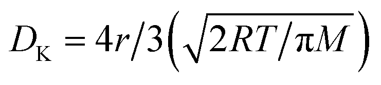 , described above), higher weight (M) molecules have a slower diffusion constant (DK) and, hence, less diffusivity in porous materials.23 Therefore, gas selectivity can be achieved through controlling the pore sizes of nanostructures. For example, H2 selectivity (diffusivity and reactivity) has been improved via employing porous SnO2 compared to a non-porous SnO2 surface.23 Selectivity improvements of a particular sensing surface can be achieved based on the electron affinity of the target gaseous molecules. According to Zhang et al., lower electron affinity molecules offer higher sensitivity, even at lower activation energies (temperatures).7 A composite form of SnO2-graphene showed better H2 selectivity than for CO and NO, possibly due to the lower electron affinity of H2.7
Repeatability is one of the essential factors for any product to obtain commercial approval. We cannot produce 100% accurate replicates of results between two sensor devices, even if the same fabrication process is followed. There must be a small percentage of dissimilarity between the outcomes from two devices, even if they are taken from the same batch. However, one can efficiently reduce the percentage error drastically via adopting careful strategies during the fabrication steps. In addition, synthesis techniques such as spin-coating and dielectrophoretic assembly are found to offer excellent consistency and controllability in outcome, even in terms of device-to-device variations.63 In most devices, reliability issues are related to the weak attachment of nanostructures to the substrate or changes in the crystallinity of the material. Vertically oriented nanostructures produce tensile stress and strain on a substrate. Therefore, deformation of the substrate crystal structure possibly reduces the robustness of the device. Furthermore, sensor devices become less robust due to environment variations, especially temperature, pressure, humidity, etc. The reliability or mechanical robustness of sensor devices can be increased via fabrication on flexible substrates.136 Sensors on flexible substrates offer the possibility for direct synthesis on the substrate, the strong bonding of nanostructures to the substrate, and lower fabrication costs. It is worth mentioning that each sensor device must undergo mechanical reliability testing on curved surfaces (positively bent and negatively bent) before being commercialized.
Conclusions
Gas sensing based on nanostructured metal oxides has been reviewed in the present article. Details relating to gas sensing with special emphasis on (i) sensor device structures (MIM, MIS, resistive, and TFT), (ii) the effects of nanostructure dimensionality, (iii) the role of contact electrodes, and (iv) issues like selectivity, repeatability, and reliability have been investigated critically. The following observations can be made: (a) resistive devices offer a higher sensor response; (b) a fast response can be obtained from vertical devices (MIS and MIM); (c) room temperature sensing is possible with TFT devices; and (d) capacitive sensors are more selective towards specific gases based on the operating frequency. Recovery problems associated with TFT-based room temperature sensing can be accelerated via the use of frequent UV illumination or light irradiation. The governing factors for the formation of materials with different dimensionality, including precursors, temperatures, pressures, etc., have also been taken into consideration in detail. The present review could provide very useful guidelines for the science and engineering community to assist them in carrying out research in the field of sensor nanotechnology.Conflicts of interest
There are no conflicts to declare.Acknowledgements
This work is supported by TEQIP-III, NIT Jamshedpur, DST India (Project Id-NIT/ECE/RP/2019).References
- B. Wang, L. F. Zhu, Y. H. Yang, N. S. Xu and G. W. Yang, Fabrication of a SnO2 Nanowire Gas Sensor and Sensor Performance for Hydrogen, J. Phys. Chem. C, 2008, 112, 6643–6647 CrossRef CAS.
- S. Y. Cho, H. W. Yoo, J. Y. Kim, W. B. Jung, M. L. Jin, J. S. Kim, H. J. Jeon and H. T. Jung, High-Resolution p-Type Metal Oxide Semiconductor Nanowire Array as an Ultrasensitive Sensor for Volatile Organic Compounds, Nano Lett., 2016, 16, 4508–4515 CrossRef CAS.
- Z. Dai, T. Liang and J. H. Lee, Gas sensors using ordered macroporous oxide nanostructures, Nanoscale Adv., 2019, 1, 1626–1639 RSC.
- T. A. Dontsova, S. V. Nahirniak and I. M. Astrelin, Metal oxide Nanomaterials and Nanocomposites of Ecological Purpose, J. Nanomater., 2019, 2019, 5942194–5942224 CrossRef.
- Y. G. Song, Y. S. Shim, S. Kim, S. D Han, H. G. Moon, M. S. Noh, K. Lee, H. R. Lee, J. S. Kim, B. K. Ju and C. Y. Kang, Downsizing Gas Sensors based on Semiconducting Metal Oxide: Effects of Electrodes on Gas Sensing Properties, Sens. Actuators, B, 2017, 248, 949–956 CrossRef CAS.
- D. Meena, B. Singh, A. Anand, M. Singh and M. C. Bhatnagar, Phase dependent selectivity shifting behavior of Cd2SnO4 nanoparticles based gas sensor towards volatile organic compounds (VOC) at low operating temperature, J. Alloys Compd., 2020, 820, 153117–153139 CrossRef CAS.
- Z. Zhang, X. Zou, L. Xu, L. Liao, W. Liu, J. Ho, X. Xiao, C. Jiang and J. Li, Hydrogen gas sensor based on metal oxide nanoparticles decorated graphene transistor, Nanoscale, 2015, 7, 10078–10084 RSC.
- J. W. Kim, Y. Porte, K. Y. Ko, H. Kim and J. M. Myoung, Micro patternable Double-Faced ZnO Nanoflowers for Flexible Gas Sensor, ACS Appl. Mater. Interfaces, 2017, 9, 32876–32886 CrossRef CAS.
- R. Jaisutti, M. Lee, J. Kim, S. Choi, T. J. Ha, J. Kim, H. Kim, S. K. Park and Y. H. Kim, Ultrasensitive Room-Temperature Operable Gas Sensors Using p-Type Na: ZnO Nanoflowers for Diabetes Detection, ACS Appl. Mater. Interfaces, 2017, 9, 8796–8804 CrossRef CAS.
- T. Guo, M. S. Yao, Y. H. Lin and C. W. Nana, A comprehensive review on synthesis methods for transition-metal oxide nanostructures, CrystEngComm, 2015, 17, 3551–3585 RSC.
- V. Inderan, M. M. Arafat, S. Kumar, A. S. M. A. Haseeb, Z. T. Jiang, M. Altarawneh and H. L. Lee, Study of structural properties and defects of Ni-doped SnO2 nanorods as ethanol gas sensors, Nanotechnology, 2017, 28, 265702–265714 CrossRef.
- F. Cao, C. Li, M. Li, H. Li, X. Huang and B. Yang, Direct growth of Al-doped ZnO ultrathin nanosheets on electrode for ethanol gas sensor application, Appl. Surf. Sci., 2018, 447, 173–181 CrossRef CAS.
- Y. Liu, Y. Jiao, Z. Zhang, F. Qu, A. Umar and X. Wu, Hierarchical SnO2 Nanostructures Made of Intermingled Ultrathin Nanosheets for Environmental Remediation, Smart Gas Sensor, and Super capacitor Applications, ACS Appl. Mater. Interfaces, 2014, 6, 2174–2184 CrossRef CAS.
- J. Zhang, S. Wang, M. Xu, Y. Wang, B. Zhu, S. Zhang, W. Huang and S. Wu, Hierarchically Porous ZnO Architectures for Gas Sensor Application, Cryst. Growth Des., 2009, 9, 3532–3537 CrossRef CAS.
- X. Xiao, L. Liu, J. Ma, Y. Ren, X. Cheng, Y. Zhu, D. Zhao, A. A. Elzatahry, A. Alghamdi and Y. Deng, Ordered Mesoporous Tin Oxide Semiconductors with Large Pores and Crystallized Walls for High-Performance Gas Sensing, ACS Appl. Mater. Interfaces, 2018, 10, 1871–1880 CrossRef CAS.
- M. Weber, J. Y. Kim, J. H. Lee, J. H. Kim, I. Iatsunskyi, E. Coy, P. Miele, M. Bechelany and S. S. Kim, Highly efficient hydrogen sensors based on Pd nanoparticles supported on boron nitride coated ZnO nanowires, J. Mater. Chem. A, 2019, 7, 8107–8116 RSC.
- D. Yang, M. K. Fuadi, K. Kang, D. Kim, Z. Li and I. Park, Multiplexed Gas Sensor Based on Heterogeneous Metal Oxide Nanomaterial Array Enabled by Localized Liquid-Phase Reaction, ACS Appl. Mater. Interfaces, 2015, 7, 10152–10161 CrossRef CAS.
- L. Chandra, R. Dwivedi and V. N. Mishra, Highly sensitive NO2 sensor using brush-coated ZnO nanoparticles, Mater. Res. Express, 2017, 4, 105030–105043 CrossRef.
- I. Rawal, Facial synthesis of hexagonal metal oxide nanoparticles for low temperature ammonia gas sensing applications, RSC Adv., 2015, 5, 4145–4142 RSC.
- B. Bhowmik and P. Bhattacharyya, A Proton Hopping-Guided 3-D Space Charge Model for Quantitative Understanding of Humidity-Dependent Gas Sensing by TiO2 Nanoflower-Based Devices, IEEE Trans. Nanotechnol., 2017, 16, 180–188 CAS.
- F. H. Babaei, M. Keshmiri, M. Kakavand and T. Troczynski, A resistive gas sensor based on undoped p-type anatase, Sens. Actuators, B, 2005, 110, 28–35 CrossRef.
- B. Bhowmik, H. Fecht and P. Bhattacharyya, Vertical Mode Gas Sensing Performance of TiO2 Nanotube Array by Tuning of Surface Area and Carrier Transport Length, IEEE Sens. J., 2015, 15, 5919–5926 CAS.
- J. Zhang, Z. Qin, D. Zeng and C. Xiea, Metal-oxide-semiconductor based gas sensors: screening, preparation, and integration, Phys. Chem. Chem. Phys., 2017, 19, 6313–6329 RSC.
- D. Han, P. Song, S. Zhang, H. Zhang, Q. Xu and Q. Wang, Enhanced methanol gas-sensing performance of Ce-doped In2O3 porous nanospheres prepared by hydrothermal method, Sens. Actuators, B, 2015, 216, 488–496 CrossRef CAS.
- X. Zhou, J. Liu, C. Wang, P. Sun, X. Hu, X. Li, K. Shimanoe, N. Yamazoe and G. Lu, Highly sensitive acetone gas sensor based on porous ZnFe2O4 nanospheres, Sens. Actuators, B, 2015, 206, 577–583 CrossRef CAS.
- T. Brezesinski, A. Fischer, K.-ichi Iimura, C. Sanchez, D. Grosso, M. Antonietti and B. M. Smarsly, Generation of Self-Assembled 3D Mesostructured SnO2 Thin Films with Highly Crystalline Frameworks, Adv. Funct. Mater., 2006, 16, 1433–1440 CrossRef CAS.
- J. Zhou, Z. Hua, Z. Liu, W. Wu, Y. Zhu and J. Shi, Direct synthetic strategy of mesoporous ZSM-5 zeolites by using conventional block copolymer templates and the improved catalytic properties, ACS Catal., 2011, 1, 287–291 CrossRef CAS.
- C. Feng, Z. Jiang, B. Chen, P. Cheng, Y. Wang and C. Huang, Aluminum-doped NiO nanofibers as chemical sensors for selective and sensitive methanol detection, Anal. Methods, 2019, 11, 575–581 RSC.
- L. Zhu and W. Zeng, Room-temperature gas sensing of ZnO-based gas sensor: a review, Sens. Actuators, A, 2017, 267, 242–261 CrossRef CAS.
- M. Fernández-Garcia and J. A. Rodriguez, Metal Oxide Nanoparticles, Wiley, 2011, DOI:10.1002/9781119951438.eibc 0331.
- Z. Dai, T. Lianga and J.-H. Lee, Gas sensors using ordered macroporous oxide nanostructures, Nanoscale Adv., 2019, 1, 1626–1639 RSC.
- A. Rao, H. Long, A. Harley-Trochimczyk, T. Pham, A. Zettl, C. Carraro and R. Maboudian, In Situ Localized Growth of Ordered Metal Oxide Hollow Sphere Array on Microheater Platform for Sensitive, Ultra-Fast Gas Sensing, ACS Appl. Mater. Interfaces, 2017, 9, 2634–2641 CrossRef CAS.
- P. Hu, G. Du, W. Zhou, J. Cui, J. Lin, H. Liu, D. Liu, J. Wang and S. Chen, Enhancement of Ethanol Vapor Sensing of TiO2 Nanobelts by Surface Engineering, ACS Appl. Mater. Interfaces, 2010, 2, 3263–3269 CrossRef CAS.
- K. Shubham, R. U. Khan and P. Chakrabarti, TiO2 Thin Film-based Low Concentration MIS Hydrogen Sensor, 2012 International Conference on Engineering (NUiCONE), Ahmedabad, 2012, pp. 1–5 Search PubMed.
- K. Dutta, P. P. Chattopadhyay, C. W. Lu, M. S. Ho and P. Bhattacharyya, A Highly Sensitive BTX Sensor based on Electrochemically Derived Wall Connected TiO2 Nanotubes, Appl. Surf. Sci., 2015, 354, 353–361 CrossRef CAS.
- L. Song, A. Lukianov, D. Butenko, H. Li, J. Zhang, M. Feng, L. Liu, D. Chen and N. I. Klyui, Facile Synthesis of Hierarchical Tin Oxide Nanoflowers with Ultra-High Methanol Gas Sensing at Low Working Temperature, Nanoscale Res. Lett., 2019, 14–24 Search PubMed.
- Y. Seekaew, A. Wisitsoraat, D. Phokharatkuland and C. Wongchoosuk, Room temperature toluene gas sensor based on TiO2 nanoparticles decorated 3D graphene-carbon nanotube nanostructures, Sens. Actuators, B, 2019, 279, 69–78 CrossRef CAS.
- Q. H. Wu, J. Li and S. G. Sun, Nano SnO2 Gas Sensor, Curr. Nanosci., 2010, 6, 525–538 CrossRef CAS.
- E. Strelcov, Y. Lilach and A. Kolmakov, Gas Sensor Based on Metal−Insulator Transition in VO2 Nanowire Thermistor, Nano Lett., 2009, 9, 2322–2326 CrossRef CAS.
- Y. J. Choi, I. S. Hwang, J. G. Park, K. J. Choi, J. H. Park and J. H. Lee, Novel fabrication of an SnO2 nanowire gas sensor with high sensitivity, Nanotechnology, 2008, 19, 095508–095512 CrossRef.
- B. Bhowmik, K. Dutta, A. Hazra and P. Bhattacharyya, Low temperature acetone detection by p-type nano-titania thin film: Equivalent circuit model and sensing mechanism, Solid-State Electron., 2014, 99, 84–92 CrossRef CAS.
- B. Bhowmik and P. Bhattacharyya, Highly stable low temperature alcohol sensor based on hydrothermally grown tetragonal titania nanorods, RSC Adv., 2015, 5, 82159–82168 RSC.
- D. Zhang, A. Liu, H. Chang and B. Xia, Room-temperature high-performance acetone gas sensor based on hydrothermal synthesized SnO2-reduced graphene oxide hybrid composite, RSC Adv., 2015, 5, 3016–3022 RSC.
- Z. Wen and L. Tian-mo, Gas sensing properties of SnO2–TiO2-based sensor for volatile organic compound gas and its sensing mechanism, Phys. B, 2010, 405, 1345–1348 CrossRef.
- B. Bhowmik and P. Bhattacharyya, Efficient Gas Sensor Devices Based on Surface Engineered Oxygen Vacancy Controlled TiO2 Nanosheets, IEEE Trans. Electron Devices, 2017, 64, 2357–2363 CAS.
- J. T. Robinson, F. K. Perkins, E. S. Snow, Z. Wei and P. E. Sheehan, Reduced graphene oxide molecular sensors, Nano Lett., 2008, 8, 3137–3140 CrossRef CAS.
- F. Hossein-Babaei and M. Orvatinia, Analysis of thickness dependence of the sensitivity in thin film resistive gas sensors, Sens. Actuators, B, 2003, 89, 256–261 CrossRef CAS.
- B. Bhowmik, A. Hazra, K. Dutta and P. Bhattacharyya, Nanocrystalline p-TiO2 based MIS device for efficient acetone detection, Sensors 2014, IEEE, Valencia, 2014, pp. 293–296, DOI:10.1109/ICSENS.2014.6984991.
- T. Qiang, C. Wang, M. Q. Liu, K. K. Adhikari, J. G. Liang, L. Wang, Y. Li, Y. M. Wu and G. H. Yanga, et al., High-Performance porous MIM-type capacitive humidity sensor realized via inductive coupled plasma and reactive-ion etching, Sens. Actuators, B, 2018, 258, 704–714 CrossRef CAS.
- A. Rao, H. Long, A. H. Trochimczyk, T. Pham, A. Zettl, C. Carraro and R. Maboudian, In Situ Localized Growth of Ordered Metal Oxide Hollow Sphere Array on Microheater Platform for Sensitive, Ultra-Fast Gas Sensing, ACS Appl. Mater. Interfaces, 2017, 9, 2634–2641 CrossRef CAS.
- N. Izu, W. Shin and N. Murayama, Fast response of resistive-type oxygen gas sensors based on nano-sized ceria powder, Sens. Actuators, B, 2003, 93, 449–453 CrossRef CAS.
- N. Izu, W. Shin, N. Murayama and S. Kanzaki, Resistive oxygen gas sensors based on CeO2 fine powder prepared using mist pyrolysis, Sens. Actuators, B, 2002, 87, 95–98 CrossRef CAS.
- P. Slobodian, P. Riha, A. Lengalova, P. Svoboda and P. Saha, Multi-wall carbon nanotube networks as potential resistive gas sensors for organic vapor detection, Carbon, 2011, 49, 2499–2507 CrossRef CAS.
- V. I. Filippov, W. Moritz, A. A. Terentjev, A. A. Vasiliev and S. S. Yakimov, Hydrocarbon and Fluorocarbon Monitoring by MIS Sensors Using an Ni Catalytic Thermodestructor, IEEE Sens. J., 2007, 7, 192–196 CAS.
- V. G. Litovchenko, T. I. Gorbanyuk, A. A. Efremov, A. A. Evtukh and D. Schipanski, Investigation of MIS gas sensitive structures with Pd and Pd/Cu metal layers, Sens. Actuators, A, 1999, 74, 233–236 CrossRef CAS.
- J. Kanungo, H. Saha and S. Basu, Room temperature metal insulator semiconductor (MIS) hydrogen sensors based on chemically surface modified porous silicon, Sens. Actuators, B, 2009, 140, 65–72 CrossRef CAS.
- P. Bhattacharyya, P. K. Basu and S. Basu, Methane Detection By Nano ZnO Based MIM Sensor Devices, Sens. Transducers J., 2011, 10, 121–130 CAS.
- A. Dutta and S. Basu, Modified metal-insulator-metal (MIM) hydrogen gas sensors based on zinc oxide, J. Mater. Sci.: Mater. Electron., 1995, 6, 415–418 CrossRef CAS.
- C. Zamania, K. Shimanoe and N. Yamazoe, A new capacitive-type NO2 gas sensor combining an MIS with a solid electrolyte, Sens. Actuators, B, 2005, 109, 216–220 CrossRef.
- T. Pham, G. Li, E. Bekyarova, M. E. Itkisand and A. Mulchandani, MoS2-Based Optoelectronic Gas Sensor with Sub-parts-per-billion Limit of NO2 Gas Detection, ACS Nano, 2019, 13, 3196–3205 CrossRef CAS.
- A. Teeramongkonrasmee and M. Sriyudthsak, Methanol and ammonia sensing characteristics of sol–gel derived thin film gas sensor, Sens. Actuators, B, 2000, 66, 256–259 CrossRef CAS.
- E. Fortunato, P. Barquinha, A. Pimentel, A. Gonçalves, A. Marques, L. Pereira and R. Martins, Recent advances in ZnO transparent thin film transistors, Thin Solid Films, 2005, 487, 205–211 CrossRef CAS.
- H. W. Zan, M. Z. Dai, T. Y. Hsu, H. C. Lin, H. F. Meng and Y. S. Yang, Porous Organic TFTs for the Applications on Real-Time and Sensitive Gas Sensors, IEEE Electron Device Lett., 2011, 32, 1143–1145 CAS.
- G. Lu, S. Park, K. Yu, Y. S. Ruoff, L. E. Ocola, D. Rosenmann and J. Chen, Toward Practical Gas Sensing with Highly Reduced Graphene Oxide: A New Signal Processing Method To Circumvent Run-to-Run and Device-to-Device Variations, ACS Nano, 2011, 5, 1154–1164 CrossRef CAS.
- M. J. Park, H. S. Jeong, H. J. Joo, H. Y. Jeong, S. H. Song and H. I. Kwon, Improvement of NO2 gas-sensing properties in InGaZnO thin-film transistors by a pre-biasing measurement method, Semicond. Sci. Technol., 2019, 34, 065010–065020 CrossRef CAS.
- Z. Gergintschew, P. Kometzky and D. Schipanski, The capacitively controlled field effect transistor (CCFET) as a new low power gas sensor, Sens. Actuators, B, 1996, 36, 285–289 CrossRef CAS.
- P. K. Basu, P. Bhattacharyya, N. Saha, H. Saha and S. Basu, The superior performance of the electrochemically grown ZnO thin films as methane sensor, Sens. Actuators, B, 2008, 133, 357–363 CrossRef CAS.
- R. Kumar, N. Goel and M. Kumar, UV-Activated MoS2 Based Fast and Reversible NO2 Sensor at Room Temperature, ACS Sens., 2017, 2, 1744–1752 CrossRef CAS.
- J. Paul and J. Philip, Inter-digital capacitive ethanol sensor coated with cobalt ferrite nanocomposite as gas sensing material, Mater. Today: Proc., 2020, 25, 148–150 CAS.
- N. L. Teradal, S. Marx, A. Morag and R. Jelinek, Porous graphene oxide chemi-capacitor vapor sensor array, J. Mater. Chem. C, 2017, 5, 1128–1135 RSC.
- R. K. Nahar and V. K. Khanna, A study of capacitance and resistance characteristics of an Al2O3 humidity sensor, Int. J. Electron., 1982, 52, 557–567 CrossRef CAS.
- N. S. Ramgir, M. Kaur, P. K. Sharma, N. Datta, S. Kailasaganapathi, S. Bhattacharya, A. K. Debnath, D. K. Aswal and S. K. Gupta, Ethanol sensing properties of pure and Au modified ZnO nanowires, Sens. Actuators, B, 2013, 187, 313–318 CrossRef CAS.
- X. Yang, H. Li, T. Li, Z. Li, W. Wu, C. Zhou, P. Sun and F. Liu, et al., Highly efficient ethanol gas sensor based on hierarchical SnO2/Zn2SnO4 porous spheres, Sens. Actuators, B, 2019, 282, 339–346 CrossRef CAS.
- S. Shao, W. Wang, Y. Chen, Y. Wang and R. Koehn, Ultrasensitive room-temperature ethanol detection based on Au functionalized nanoporous SnO2/C60/SnO2 composites, RSC Adv., 2017, 7, 53925–53931 RSC.
- C. Wang, X. Kou, N. Xie, L. Guo, Y. Sun, X. Chuai, J. Ma, P. Sun, Y. Wang and G. Lu, Detection of Methanol with Fast Response by Mono dispersed Indium Tungsten Oxide Ellipsoidal Nanospheres, ACS Sens., 2017, 2, 648–654 CrossRef CAS.
- H. M. Yang, S. Y. Ma, G. J. Yang, W. X. Jin, T. T. Wang, X. H. Jiang and W. Q. Li, High sensitive and low concentration detection of methanol gas sensor based on one-step synthesis αFe2O3 hollow spheres, Mater. Lett., 2016, 169, 73–76 CrossRef CAS.
- Y. J. Chen, X. Y. Xue, Y. G. Wang and T. H. Wang, Synthesis and ethanol sensing characteristics of single crystalline SnO2 nanorods, Appl. Phys. Lett., 2005, 87, 233503–233506 CrossRef.
- L. Mei, J. Deng, X. Yin, M. Zhang, Q. Li, E. Zhang, Z. Xu, L. Chen and T. Wang, Ultrasensitive ethanol sensor based on 3D aloe-like SnO2, Sens. Actuators, B, 2012, 166–167, 7–11 CrossRef CAS.
- M. Z. Ahmad, A. Z. Sadek, K. Latham, J. Kita, R. Moos and W. Wlodarski, Chemically synthesized one-dimensional zinc oxide nanorods for ethanol sensing, Sens. Actuators, B, 2013, 187, 295–300 CrossRef CAS.
- G. Singh, Virpal and R. C. Singh, Highly sensitive gas sensor based on Er-doped SnO2 nanostructures and its temperature dependent selectivity towards hydrogen and ethanol, Sens. Actuators, B, 2019, 282, 373–383 CrossRef CAS.
- A. S. Zoolfakar, M. Z. Ahmad, R. A. Rani, J. Z. Ou, S. Balendhran, S. Zhuiykov, K. Latham, W. Wlodarski and K. Kalantar-Zadeh, Nanostructured copper oxides as ethanol vapour sensors, Sens. Actuators, B, 2013, 185, 620–627 CrossRef CAS.
- R. Pandeeswari, R. K. Karnand and B. G. Jeyaprakash, Ethanol sensing behaviour of sol–gel dip-coated TiO2 thin films, Sens. Actuators, B, 2014, 194, 470–477 CrossRef CAS.
- R. Peng, J. Chen, D. Li, L. Chen and L. Ci, Investigation of the gas-sensitive properties for methanol detection based on ZnO/SnO2 heterostructure, IOP Conf. Ser.: Mater. Sci. Eng., 2018, 392, 032016–032020 Search PubMed.
- J. Qin, Z. Cui, X. Yang, S. Zhu, Z. Li and Y. Liang, Three-dimensionally ordered macro porous La1-xMgxFeO3 as high performance gas sensor to methanol, J. Alloys Compd., 2015, 635, 194–202 CrossRef CAS.
- Y. Li, D. Deng, N. Chen, X. Xing, X. Xiao and Y. Wang, Enhanced methanol sensing properties of SnO2 microspheres in a composite with Pt nanoparticles, RSC Adv., 2016, 6, 83870–83879 RSC.
- Y. Shen, A. Fan, D. Wei, S. Gao, W. Liu, C. Han and B. Cui, A low-temperature n-propanol gas sensor based on TeO2 nanowires as the sensing layer, RSC Adv., 2015, 5, 29126–29130 RSC.
- C. Dong, X. Xing, N. Chen, X. Liu and Y. Wang, Biomorphic synthesis of hollow CuOfibers for low-ppm-level n-propanol detection via a facile solution combustion method, Sens. Actuators, B, 2016, 230, 1–8 CrossRef CAS.
- Y. Yin, Y. Shen, P. Zhou, R. Lu, A. Li, S. Zhao, W. Liu, D. Wei and K. Wei, Fabrication, characterization and n-propanol sensing properties of perovskite-type ZnSnO3 nanospheres based gas sensor, Appl. Surf. Sci., 2020, 509 DOI:10.1016/j.apsusc.2020.145335.
- M. Mori, Y. Itagaki, J. Iseda, Y. Sadaoka, T. Ueda, H. Mitsuhashi and M. Nakatani, Influence of VOC structures on sensing property of SmFeO3 semiconductive gas sensor, Sens. Actuators, B, 2014, 202, 873–877 CrossRef CAS.
- M. Li, H. Zhu, B. Wang, J. Cheng, W. Yan, S. Xia and Z. Tang, Ultrasensitive and highly selective detection of methoxy propanol based on Ag-decorated SnO2 hollow nanospheres, Sens. Actuators, B, 2016, 232, 545–556 CrossRef CAS.
- Q. Zhang, F. Meng, L. Zha, X. Wang and G. Zhang, A sensitive cataluminescence-based sensor using a SrCO3/graphene composite for n-propanol, RSC Adv., 2015, 5, 57482–57489 RSC.
- A. K. Vishwakarma and L. Yadav, Detection of propanol gas using titanium dioxide based thick film, IOP Conf. Ser.: Mater. Sci. Eng., 2018, 404, 012020–012024 CrossRef.
- L. Wang, R. Zhang, T. Zhou, Z. Lou, J. Deng and T. Zhang, Concave Cu2O octahedral nanoparticles as an advanced sensing material for benzene (C6H6) and nitrogen dioxide (NO2) detection, Sens. Actuators, B, 2016, 223, 311–317 CrossRef CAS.
- L. Yu, H. Song, Y. Tang, L. Zhang and Y. Lv, Controllable deposition of ZnO-doped SnO2 nanowires on Au/graphene and their application in cataluminescence sensing for alcohols and ketones, Sens. Actuators, B, 2014, 203, 726–735 CrossRef CAS.
- Y. Zeng, T. Zhang, M. Yuan, M. Kang, G. Lu, R. Wang, H. Fan, Y. He and H. Yang, Growth and selective acetone detection based on ZnO nanorod arrays, Sens. Actuators, B, 2009, 143, 93–98 CrossRef.
- L. Sui, X. Zhang, X. Cheng, P. Wang, Y. Xu, S. Gao, H. Zhao and L. Huo, Au-loaded hierarchical MoO3 hollow spheres with enhanced gas sensing performance for the detection of BTX (benzene, toluene and xylene) and the sensing mechanism, ACS Appl. Mater. Interfaces, 2017, 9, 1661–1670 CrossRef CAS.
- Z. Shen, X. Zhang, X. Ma, R. Mi, Y. Chen and S. Ruan, The significant improvement for BTX sensing performance based on Au-decorated hierarchical ZnO porous rose-like architectures, Sens. Actuators, B, 2018, 262, 86–94 CrossRef CAS.
- D. Acharyya and P. Bhattacharyya, An efficient BTX sensor based on ZnO nanoflowers grown by CBD method, Solid-State Electron., 2015, 106, 18–26 CrossRef CAS.
- A. Ndiaye, P. Bonnet, A. Pauly, M. Dubois, J. Brunet, C. Varenne, K. Guerin and B. Lauron, Noncovalent Functionalization of Single-Wall Carbon Nanotubes for the Elaboration of Gas Sensor Dedicated to BTX Type Gases: The Case of Toluene, J. Phys. Chem. C, 2013, 117, 20217–20228 CrossRef CAS.
- A. Pauly, J. Brunet, C. Varenne and A. L. Ndiaye, Insight in the interaction mechanisms between functionalized CNTs and BTX vapors in gas sensors: are the functional peripheral groups the key for selectivity?, Sens. Actuators, B, 2019, 298, 126768–126778 CrossRef CAS.
- P. P. Sahay, Zinc oxide thin film gas sensor for detection of acetone, J. Mater. Sci., 2005, 40, 4383–4385 CrossRef CAS.
- G. Li, Z. Cheng, Q. Xiang, L. Yan, X. Wang and J. Xu, Bimetal Pd Au decorated SnO2 nanosheets based gas sensor with temperature-dependent dual selectivity for detecting formaldehyde and acetone, Sens. Actuators, B, 2019, 283, 590–601 CrossRef CAS.
- T. Zhoua, T. Zhang, J. Deng, R. Zhang, Z. Lou and L. Wang, P-type Co3O4 nanomaterials-based gas sensor: preparation and acetone sensing performance, Sens. Actuators, B, 2017, 242, 369–377 CrossRef.
- M. E. DMello, N. G. Sundaram and S. B. Kalidindi, Assembly of ZIF-67 Metal–Organic Framework over Tin Oxide Nanoparticles for Synergistic Chemiresistive CO2 Gas Sensing, Chem.–Eur. J., 2018, 24, 9220–9223 CrossRef CAS.
- V. S. Bhati, S. Ranwa, S. Rajamani, K. Kumari, R. Raliya, P. Biswas and M. Kumar, Improved sensitivity with low limit of detection of hydrogen gas sensor based on rGO loaded Ni doped ZnO nanostructures, ACS Appl. Mater. Interfaces, 2018, 10, 11116–11124 CrossRef CAS.
- D. Kim, P. V. Pikhitsa, H. Yang and M. Choi, Room temperature CO and H2 sensing with carbon nanoparticles, Nanotechnology, 2011, 22, 485501–485508 CrossRef.
- S. G. Surya, S. Bhanoth, S. M. Majhi, Y. D. More, V. M. Teja and K. N. Chappanda, A silver nanoparticle-anchored UiO-66(Zr) metal–organic framework (MOF)-based capacitive H2S gas sensor, CrystEngComm, 2019, 21, 7303–7312 RSC.
- A. A. Yadav, A. C. Lokhande, J. H. Kim and C. D. Lokhande, Enhanced sensitivity and selectivity of CO2 gas sensor based on modified La2O3 nanorods, J. Alloys Compd., 2017, 723, 880–886 CrossRef CAS.
- X. Xue, Z. Chen, C. Ma, L. Xing, Y. Chen, Y. Wang and T. Wang, One-Step Synthesis and Gas-Sensing Characteristics of Uniformly Loaded Pt@SnO2Nanorods, J. Phys. Chem. C, 2010, 114, 3968–3972 CrossRef CAS.
- G. J. Sun, J. K. Lee, S. Choi, W. I. Lee, H. W. Kim and C. Lee, Selective oxidizing gas sensing and dominant sensing mechanism of n-CaO-decorated n-ZnO nanorod sensors, ACS Appl. Mater. Interfaces, 2017, 9, 9975–9985 CrossRef CAS.
- X. Wang, F. Sun, Y. Duan, Z. Yin, W. Luo, Y. A. Huang and J. Chen, Highly sensitive, temperature-dependent gas sensor based on hierarchical ZnO nanorod arrays, J. Mater. Chem. C, 2015, 3, 11397–11405 RSC.
- C. Wang, X. Cui, J. Liu, X. Zhou, X. Cheng, P. Sun, X. Hu, X. Li, J. Zheng and G. Lu, The Design of Superior Ethanol Gas Sensor Based on the Al-Doped NiO Nanorod-Flowers, ACS Sens., 2016, 1, 131–136 CrossRef CAS.
- H. Nguyen and S. A. El-Safty, Meso- and Macroporous Co3O4 Nanorods for Effective VOC Gas Sensors, J. Phys. Chem. C, 2011, 115, 8466–8474 CrossRef CAS.
- B. S. Kang, Y. W. Heo, L. C. Tien, D. P. Norton, F. Ren, B. P. Gila and S. J. Pearton, Hydrogen and ozone gas sensing using multiple ZnO nanorods, Appl. Phys. A, 2005, 80, 1029–1032 CrossRef CAS.
- A. Ayeshamariam, D. Saravanakkumar, M. Kashif, S. Sivaranjani and B. Ravikumar, Analysis on the effect of ZnO on Carbon nanotube by spray pyrolysis method, Mechanics of Advanced Materials and Modern Processes, 2016, 2, 3 CrossRef.
- L. Hou, C. Zhang, L. Li, C. Du, X. Li, X. F. Kang and W. Chen, CO Gas Sensors based on p-type CuO Nanotubes and CuONanocubes: Morphology and Surface Structure Effects on the Sensing Performance, Talanta, 2018, 188, 41–49 CrossRef CAS.
- M. Han, J. K. Kim, G. S. Lee, S. W. Kang and D. Jung, A CO gas sensor based on Pt-loaded carbon nanotube sheets, Jpn. J. Appl. Phys., 2019, 58, SDDE03–SDDE08 CrossRef CAS.
- R. Li, K. Jiang, S. Chen, Z. Lou, T. Huang, D. Chen and G. Shen, SnO2/SnS2 nanotubes for flexible room temperature NH3 gas sensor, RSC Adv., 2017, 7, 52503–52509 RSC.
- Z. Yang, C. Su, S. Wang, Y. Han, X. Chen, S. Xu, Z. Zhou, N. Hu, Y. Su and M. Zeng, Highly sensitive NO2 gas sensors based on hexagonal SnS2 nanoplates operating at room temperature, Nanotechnology, 2019, 31, 075501–075530 CrossRef.
- Z. Li, N. Wang, Z. Lin, J. Wang, W. Liu, K. Sun, Y. Q. Fu and Z. Wang, Room-temperature high performance H2S sensor based on porous CuO nanosheets prepared by hydrothermal method, ACS Appl. Mater. Interfaces, 2016, 8, 20962–20968 CrossRef CAS.
- J. Li, H. Fan and X. Jia, Multilayered ZnO Nanosheets with 3D Porous Architectures: Synthesis and Gas Sensing Application, J. Phys. Chem. C, 2010, 114, 14684–14691 CrossRef CAS.
- Z. Chen, J. Wang, A. Umar, Y. Wang, H. Li and G. Zhou, Three-Dimensional Crumpled Graphene-Based Nanosheets with Ultrahigh NO2 Gas Sensibility, ACS Appl. Mater. Interfaces, 2017, 9, 11819–11827 CrossRef CAS.
- F. Zhang, A. Zhu, Y. Luo, Y. Tian, J. Yang and Y. Qin, CuO Nanosheets for Sensitive and Selective Determination of H2S with High Recovery Ability, J. Phys. Chem. C, 2010, 114, 19214–19219 CrossRef CAS.
- M. Tonezzer, Selective gas sensor based on one single SnO2 nanowire, Sens. Actuators, B, 2019, 288, 53–59 CrossRef CAS.
- X. Wang, Z. Xie, H. Huang, Z. Liu, D. Chen and G. Shen, Gas sensors, thermistor and photodetector based on ZnS nanowires, J. Mater. Chem., 2012, 22, 6845–6850 RSC.
- M. Sinha, R. Mahapatra, B. Mondal, T. Maruyama and R. Ghosh, Ultra-fast and Reversible Gas Sensing Properties Of ZnO Nanowire Arrays Grown By Hydrothermal Technique, J. Phys. Chem. C, 2016, 120, 3019–3025 CrossRef CAS.
- M. W. Ahn, K. S. Park, J. H. Heo, J. G. Park, D. W. Kim, K. J. Choi, J. H. Lee and S. H. Hong, Gas sensing properties of defect-controlled ZnO-nanowire gas sensor, Appl. Phys. Lett., 2008, 93, 263103–263106 CrossRef.
- T. Y. Hwang, G. M. Go, S. Park, J. Lee, Y. Song, S. Kim, H. B. Cho and Y. H. Choa, Pt/graphene Catalyst and Tellurium Nanowire-based Thermochemical Hydrogen (TCH) Sensor Operating at Room Temperature in Wet Air, ACS Appl. Mater. Interfaces, 2019, 11, 47015–47024 CrossRef CAS.
- L. Yang, Z. Wang, X. Zhou, X. Wu, N. Han and Y. Chen, Synthesis of Pd-loaded mesoporous SnO2 hollow spheres for highly sensitive and stable Methane gas sensors, RSC Adv., 2018, 8, 24268–24275 RSC.
- L. Ge, X. Jing, J. Wang, J. Wang, S. Jamil, Q. Liu, F. Liuand and M. Zhang, Trisodium citrate assisted synthesis of ZnO hollow spheres via a facile precipitation route and their application as gas sensor, J. Mater. Chem., 2011, 21, 10750–10754 RSC.
- X. Zhou, W. Feng, C. Wang, X. Hu, X. Li, P. Sun, K. Shimanoe, N. Yamazoe and G. Lu, Porous ZnO/ZnCo2O4 hollow spheres: synthesis, characterization, and applications in gas sensing, J. Mater. Chem. A, 2014, 2, 17683–17690 RSC.
- D. Acharyya, N. Banerjee and P. Bhattacharyya, A comparative study on methanol sensing performance of ZnO nanoflower and nanorod based resistive devices, Sensors 2014, IEEE, Valencia, 2014, pp. 811–814, DOI:10.1109/ICSENS.2014.6985123.
- J. Hu, C. Zou, Y. Su, M. Li, Y. Han, E. S. W. Kong, Z. Yang and Y. Zhang, Ultrasensitive NO2 gas sensor based on hierarchical Cu2O/CuOmesocrystals nanoflower, J. Mater. Chem. A, 2018, 6, 17120–17131 RSC.
- S. P. Lee, Electrodes for Semiconductor Gas Sensors, Sensors, 2017, 17, 683–702 CrossRef.
- S. Capone, P. Siciliano, F. Quaranta, R. Rella, M. Epifani and L. Vasanelli, Moisture influence and geometry effect of Au and Pt electrodes on CO sensing response of SnO2 microsensors based on sol-gel thin film, Sens. Actuators, B, 2001, 77, 503–511 CrossRef CAS.
- Z. Wang, T. Han, T. Fei, S. Liu and T. Zhang, Investigation of Microstructure Effect on NO2 Sensors Based on SnO2 Nanoparticles/Reduced Graphene Oxide Hybrids, ACS Appl. Mater. Interfaces, 2018, 10, 41773–41783 CrossRef CAS.
- O. Lupan, V. Postica, J. Gröttrup, A. K. Mishra, N. H. Leeuw, J. F. C. Carreira, J. Rodrigues, N. B. Sedrine, M. R. Correia and T. Monteiro, et al., Hybridization of Zinc Oxide Tetrapods for Selective Gas Sensing Applications, ACS Appl. Mater. Interfaces, 2017, 9, 4084–4099 CrossRef CAS.
- M. Frietsch, F. Zudock, J. Goschnick and M. Bruns, CuO catalytic membrane as selectivity trimmer for metal oxide gas sensors, Sens. Actuators, B, 2000, 65, 379–381 CrossRef CAS.
- X. Zou, J. Wang, X. Liu, C. Wang, Y. Jiang, Y. Wang, X. Xiao and J. C. Ho, et al., Rational Design of Sub-Parts per Million Specific Gas Sensors Array Based on Metal Nanoparticles Decorated Nanowire Enhancement-Mode Transistors, Nano Lett., 2013, 13, 3287–3292 CrossRef CAS.
| This journal is © The Royal Society of Chemistry 2021 |