
 Open Access Article
 This Open Access Article is licensed under a
 Creative Commons Attribution 3.0 Unported Licence
n Bu2Sn(SnBu)2 and nBu3SnEnBu (E = S or Se) – effective single source precursors for the CVD of SnS and SnSe thermoelectric thin films†
Fred
Robinson
 a,
Peter J.
Curran
b,
C. H. (Kees)
de Groot
c,
Duncan
Hardie
b,
Andrew L.
Hector
a,
Katherine
Holloway
a,
Ruomeng
Huang
c,
Daniel
Newbrook
c and
Gillian
Reid
*a
a,
Peter J.
Curran
b,
C. H. (Kees)
de Groot
c,
Duncan
Hardie
b,
Andrew L.
Hector
a,
Katherine
Holloway
a,
Ruomeng
Huang
c,
Daniel
Newbrook
c and
Gillian
Reid
*a
aSchool of Chemistry, University of Southampton, Southampton SO17 1BJ, UK. E-mail: G.Reid@soton.ac.uk
bDeregallera Ltd, Unit 2, De Clare Court, Pontygwindy Industrial Estate, Caerphilly CF83 3HU, UK
cSchool of Electronics and Computer Science, University of Southampton, Southampton SO17 1BJ, UK
First published on 17th June 2021
Abstract
The use of single source precursors offers a convenient option for the chemical vapour deposition of thin film semiconductor materials with good stoichiometric control and precursor efficiency. Here we show that reaction of nBu3SnCl with NaSnBu or LiSenBu, or nBu2SnCl2 with 2 mol equiv. of NaSnBu, gives the molecular alkyltin chalcogenolate precursors, nBu3SnEnBu (E = S (1), Se (3)) and nBu2Sn(SnBu)2 (2), respectively, in good yield as colourless (S) or yellow/orange (Se) oils. These were characterised by 1H, 13C{1H}, 77Se{1H} and 119Sn{1H} NMR spectroscopy, microanalysis and thermogravimetric analysis. Low pressure CVD experiments using these precursors showed that (1) gave S-deficient SnS thin films, whereas using (2) and implementing short deposition times and low precursor loadings, gave stoichiometric SnS films. Stoichiometric SnSe films were also obtained using (3) and confirmed by grazing incidence XRD analysis, which revealed the films adopt the orthorhombic Pnma structure. SEM and EDX analysis, together with Raman spectroscopic data, were also used to identify the films deposited and to correlate with the deposition conditions employed. Variable temperature Seebeck and Hall effect characterisation confirm that the stoichiometric SnS and SnSe films are semiconducting and highly resistive, giving large positive Seebeck coefficients, with the overall power factor ranging from 0.017 at 300 K to 0.049 μW cm−1 K−2 at 450 K for SnS and increasing from 0.06 at 300 K to 0.4 μW cm−1 K−2 at 425 K for SnSe.
Introduction
The group 14 monochalcogenides, ME (M = Pb, Sn, Ge; E = S, Se, Te) are semiconducting materials with significant technological importance. As layered materials in which the M–E bonding in-plane is strong, while weak van der Waals interactions prevail between layers, they can be considered as graphene analogues, although with the key advantages that their band-gaps may be tuned through variation of M or E, and they exhibit increased stability in air. These materials are of significant interest for a range of energy applications, including for incorporation into thermoelectric devices for energy harvesting.Thermoelectric (TE) materials allow for the conversion of heat energy to electrical energy, when a temperature gradient is applied across the material, via the Seebeck effect.1 As such they have significant potential for the scavenging of wasted heat. The loss of heat during the production of energy via the burning of coal, natural gas, oil and nuclear power is accountable for the loss of ca. 60% of the energy generated.2 With growing concerns regarding carbon emissions, TE materials are forming a cornerstone of global efforts to reduce CO2 emissions and arrest the climate emergency. If suitable materials and industrially relevant, scalable and flexible processes can be developed, ubiquity for TE devices beckons. Furthermore, TE microgenerators have no moving parts, are silent and typically produce small voltages,3 which means they are suited to power generation for small sensors compatible with applications in the internet of things (IoT).4,5
One useful way that TE materials can be compared to one another is through their respective unitless figures of merit, 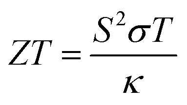 , which contains the Seebeck coefficient (S), the electrical conductivity (σ), the average temperature across the material (T) and the thermal conductivity of the material (κ). While it is important to note that the ZT value alone does not guarantee good efficiency (measured from the power in vs. the power out) in an actual TE device, a high ZT value can identify promising materials worth pursuing and optimising in order to produce a fabricated device.
There are a number of reported examples of tin monochalcogenides, SnE (E = S, Se), that display exciting TE performances,6–11 of particular note is SnSe, single crystals of which have been reported to have a high peak ZT of 2.8 at 773 K.12 Interest in tin sulfide as a TE material stems from its structural similarities to tin selenide as well as the high natural abundance and low cost of sulfur. The low thermal conductivity of tin sulfide and selenide is partly attributed to the layered orthorhombic structure in their crystalline forms,7,8,13,14 where the distance between layers interrupts the movement of phonons, while simultaneously allowing for electrical transport.12 The tuneable band gaps expressed by tin chalcogenides15 also lead to a range of other exciting applications for these materials in photovoltaics, photocatalysis, photonics, optoelectronics and as battery materials.16–18
The growth of tin chalcogenide thin films has been reported using a number of deposition techniques, including aerosol assisted chemical vapour deposition (AACVD), atmospheric pressure (AP) CVD and atomic layer deposition (ALD).15,19–24 These deposition techniques have used both dual and single source precursors (SSPs). SSPs are highly beneficial as they provide a simple means of controlling the stoichiometry of the elements in the deposit, as well as affecting the material growth by subtle changes to the SSP design. Some SSPs have also been shown to allow for selective deposition of materials into patterned substrates.25–31 The use of low pressure CVD with SSPs is especially beneficial when compared to the above deposition techniques as the precursors suitable for LPCVD are the most versatile and more transferable to other deposition methodologies.
In the literature, SnS films are typically deposited using dual source precursors such as SnCl4 and H2S. Aside from the hazards associated with these reagents, dual source CVD techniques rely on strict engineering controls to regulate the stoichiometry of the deposited material. Previous SSPs established within our own group, [SnCl4(nBuE{CH2}3EnBu)] (E = S or Se), were shown to produce films of SnS2 or SnSe2via low pressure CVD, while at elevated temperatures films of the monochalcogenides, SnS or SnSe, can be produced.32 Examples of other reported SSPs include, [{RNC(NMe2)NR}Sn(E)] (R = Cy, E = S and R = iPr or Cy when E = Se),15 [SnnBu2(S2CN(R)2)2] (R = Et, Me, nBu),33 [Sn(SeCOC6H6)2Bu2],34 [Sn(SCH2CH2S)2],35 [Bz3SnCl(L)] (where L is thiosemicarbazones of salicylaldehyde or 4-chlorobenzaldehyde),36 [Sn(Ph2PSe2)2]37 and [Sn({C6H5}NCSN{Me2})(NMe2)],38 all of which have shown good quality deposits of SnS or SnSe. However, due to either the instability or low volatilities of these SSPs, film deposition required aerosol-assisted CVD processes. Thus, a family of precursors capable of depositing high quality thin films of SnE (E = S or Se) reproducibly by low pressure CVD would allow for the depositions to occur without the requirement for solvation and nebulisation. This may lead to greater control over the growth of the material as there is no solvent evaporation process.
While the organometallic compounds, [SnnBu3(SnBu)] (1), [SnnBu2(SnBu)2] (2) and [SnnBu3(SenBu)] (3), have been described briefly previously,39,40 the experimental procedures and characterisation lacked detail. Hence, we report here full descriptions of their preparations and spectroscopic analysis, together with their TGA data and the application of these compounds as single source precursors for the deposition of thin films of SnS and SnSe. The resulting films are characterised by XRD, SEM, EDX and Raman spectroscopy and we present the thermoelectric measurements, including variable temperature Seebeck, electrical conductivity and power factor, along with variable temperature Hall effect coefficients, charge carrier concentrations and mobility measurements for samples of SnSe and SnS. The heavier tellurolate analogue, [SnnBu3(TenBu)], has recently been shown to be an effective precursor for the growth of SnTe thin films by low pressure CVD.41
Experimental
All precursor syntheses were performed under an inert atmosphere using Schlenk, vacuum line and glove box techniques under a dry nitrogen atmosphere. The solvents used (THF, toluene and hexane) were dried by distillation from sodium wire prior to use and NMR solvents were stored in a glovebox over molecular sieves. nBu3SnCl, nBu2SnCl2 (Alfa Aesar) and butane thiol (Aldrich) were stored in a glovebox and used as received. All 1H, 13C{1H}, 77Se{1H} (the latter referenced against neat SeMe2) and 119Sn{1H} (referenced against neat SnMe4) NMR spectra were collected at 298 K using a Bruker AV400 spectrometer in CDCl3 (without the need for a relaxation agent). Microanalyses were obtained via the London Metropolitan University elemental analysis service.The volatilities of the precursors were determined using a temperature ramp experiment via TGA. This experiment was conducted by measuring approximately 20 mg of each precursor into an alumina crucible inside a dry, nitrogen-filled glove box. The crucible was then quickly transferred to the TGA where it was immediately put under a flow of argon gas. The precursor was then heated at a ramp rate of 5 °C min−1 under a constant flow of argon gas from 30–600 °C while the mass loss was monitored.
[SnnBu3(SnBu)] (1)
Butane thiol (0.949 g, 1.05 × 10⁻² mol) was added to a solution of sodium metal (0.242 g, 1.05 × 10⁻² mol) dissolved in anhydrous ethanol (20 mL) and stirred vigorously over the course of 2 h. Removal of volatiles from this colourless solution gave a white powder. THF (20 mL) was then added, followed by a solution of tributyltin chloride (3.877 g, 9.49 × 10⁻³ mol) in THF (20 mL), which was added dropwise over the course of 5 min, resulting in a cloudy white suspension, which was stirred for 12 h. The reaction mixture was then filtered, producing a clear, colourless solution. After the THF had been removed under vacuum, the clear colourless liquid remaining was washed in anhydrous hexane (30 mL), filtered to remove particulates and dried in vacuo. Yield: 2.618 g, 73%. Elemental analysis: calc. for C16H36SSn (379.20 g mol−1): C 50.66, H 9.57%. Found: C 50.89, H 10.13%. 1H NMR (CDCl3): δ/ppm = 0.84 (two overlapping t, J = 8.00 Hz, [12H], CH3), 1.06 (t with 119Sn satellites, [6H], CH2Sn), 1.26 (overlapping m, [8H], CH2), 1.50 (overlapping m, [8H], CH2) 2.48 (t, [2H], CH2S). 13C{1H} NMR (CDCl3): δ/ppm = 13.33 (1J119Sn13C = 333 Hz, 1J117Sn13C = 317 Hz, CH2), 13.60 (CH3), 13.62 (CH3), 21.84 (CH2), 26.40 (CH2), 27.06 (2J119Sn13C = 60 Hz, CH2), 28.65 (3J119Sn13C = 21 Hz, CH2), 37.03 (2J119Sn13C = 12 Hz CH2). 119Sn {1H} NMR (CDCl3): δ/ppm = 75.2 (s).[SnnBu2(SnBu)2] (2)
Butane thiol (0.878 g, 9.73 × 10⁻³ mol) was added to a solution of sodium metal (0.224 g, 9.73 × 10⁻³ mol) dissolved in anhydrous ethanol (20 mL) and stirred vigorously for 1 h. This colourless solution was then taken to dryness in vacuo, leaving a white powder. This white powder was then suspended in THF (15 mL) and a solution of dibutyltin dichloride (1.478 g, 4.86 × 10⁻³ mol), in THF (15 mL), was added dropwise over the course of 5 min, resulting in a cloudy white suspension, which was stirred for 12 h. The reaction mixture was then filtered, producing a clear colourless solution. After the THF had been removed under vacuum, a colourless oil remained, which was washed with anhydrous hexane (20 mL) and dried in vacuo. Yield: 1.407 g, 70%. Elemental analysis: calc. for C16H36S2Sn (411.26 g mol−1): C 46.73, H 8.82%. Found: C 45.96, H 9.44%. 1H NMR (CDCl3): δ/ppm = 0.91 (two overlapping t, J = 8.00 Hz, [12H], CH3), 1.39 (overlapping tqrt, tt and t with 119Sn satellites, [12H], CH2 and SnCH2), 1.58 (overlapping tqrt and tt, [8H], CH2), 2.69 (t, [8H], SCH2). 13C {1H} NMR (CDCl3): δ/ppm = 13.52 (CH3), 13.59 (CH2), 17.79 (1J119Sn13C = 377 Hz, 1J117Sn13C = 360 Hz, CH3), 21.77 (CH2), 26.70 (2J119Sn13C = 73 Hz, 2J117Sn13C = 70 Hz CH2), 26.98 (3J119Sn13C = 16 Hz, CH2), 28.24 (2J119Sn13C = 25 Hz, CH2), 36.51 (3J119Sn13C = 14 Hz, CH2). 119Sn{1H} NMR (CDCl3): δ/ppm = 127.6 (s).[SnnBu3(SenBu)] (3)
Selenium shot (2.041 g, 2.59 × 10⁻² mol) was ground into a fine powder under an inert atmospheric in a glovebox before being suspended in THF (30 mL). The suspension was then frozen in liquid nitrogen (77 K) before the dropwise addition of nBuLi solution in hexanes (15 mL, 2.43 × 10⁻² mol). After the mixture had thawed and been allowed to stir, a colour change from a black suspension to a yellow solution and then to a deep red solution was observed. Further nBuLi solution (1 mL, 1.60 × 10⁻³ mol) was then added dropwise until a pale yellow colour persisted. A solution of nBu3SnCl (7.650 g, 2.35 × 10⁻² mol) in THF (30 mL) was then added dropwise to the cooled (273 K) solution of nBuSeLi. The reaction mixture was then stirred vigorously overnight. The reaction mixture was then concentrated under vacuum, hexane (30 mL) was added, at which point the solution turned cloudy with the precipitation of LiCl. The mixture was filtered by cannula filter, before concentrating under vacuum, washing with further hexane (30 mL), filtering once more and finally drying in vacuo, leaving a yellow/orange oil. Yield: 7.936 g, 79%. Elemental analysis: calc. for C16H36SeSn (426.11 g mol−1): C 45.10, H 8.52%. Found: C 45.29, H 8.95%. 1H NMR (CDCl3): δ/ppm = 0.88 (two overlapping t, J = 8.00 Hz, [12H], CH3), 1.13 (t with 119Sn satellites, [6H], SnCH2), 1.29–1.40 (overlapping dt, [8H], CH2), 1.54–1.62 (overlapping dt, [8H], CH2), 2.53 (overlapping t with 77Se satellites, [2H], SeCH2). 13C{1H} NMR (CDCl3): δ/ppm = 13.07 (1J119Sn13C = 318 Hz, 1J117Sn13C = 305 Hz, CH2), 13.45 (CH2), 13.54 (CH3), 16.79 (3J77Se13C = 14 Hz, CH2), 22.90 (CH2), 26.98 (2J119Sn13C = 62 Hz, 2J117Sn13C = 60 Hz, CH2), 28.94 (3J119Sn13C = 21 Hz, CH2), 36.70 (3J119Sn13C = 11 Hz, CH2). 77Se{1H} NMR (CDCl3): δ/ppm = −213.8 (s, 1J77Se119Sn = 1050 Hz). 119Sn{1H} NMR (CDCl3): δ/ppm = 51.9 (s, 1J77Se119Sn = 1056 Hz).Thin film growth by low pressure CVD
The fused quartz substrates (1 mm × 8 mm × 20 mm) were washed with deionised water, followed by ethanol, before being dried thoroughly in an oven before use. In a typical LPCVD experiment, the precursor (5–50 mg) and fused quartz substrates were loaded into a silica CVD tube inside the glovebox. The precursor was loaded into the precursor bulb at the closed end of the tube and the substrates were positioned end-to-end lengthways (0–4 cm away from the precursor bulb) along the silica tube. The tube was positioned horizontally in the furnace and held in place such that the precursor bulb was protruding from the end of the furnace. The tube was evacuated to ca. 0.01–0.05 mmHg and the furnace was heated to the required temperature and allowed to stabilise. The tube was then repositioned so that the precursor was close enough to the furnace for evaporation to be observed. This position was then maintained until all the precursor had evaporated, typically between 10 min to 1 h. Once the deposition was complete, the tube was removed from the furnace and allowed to cool to room temperature before being transferred to the glovebox under N2, where the substrates were removed and stored for characterisation.The LPCVD experiments produced grey films of SnS and dark grey films of SnSe. All of the precursors produced uniform and continuous films with coverages of at least 6 cm2.
Thin film characterisation
Grazing incidence X-ray diffraction (XRD) patterns were collected using a Rigaku SmartLab system (Cu-Kα, λ = 1.5418 Å) with parallel X-ray beam and a Hypix detector in 1D mode. A 2θ scan range of 10–80° and an ω-offset of 1° were used The crystalline phase of the film was determined by comparison with a literature XRD pattern, accessed via the Inorganic Crystal Structure Database (ICSD),42 and lattice parameters were obtained by further optimisation of the fit using PDXL.43The SEM used was a FEI XL30 ESEM (Environmental Scanning Electron Microscope) tungsten filament electron source with ThermoFisher UltraDry EDX, 10 mm2 detector. The images were all captured at magnifications of 2000, 5000 and 10![[thin space (1/6-em)]](https://www.rsc.org/images/entities/char_2009.gif) 000 times at accelerator voltages of either 10 or 15 eV. The Raman spectra were obtained using a Renishaw inVia confocal Raman microscope with a 785 nm, 500 mW laser.
000 times at accelerator voltages of either 10 or 15 eV. The Raman spectra were obtained using a Renishaw inVia confocal Raman microscope with a 785 nm, 500 mW laser.
Thermoelectric and electrical property measurements
Variable temperature resistivity, carrier concentration and carrier mobility were determined by Hall measurements (Nanometrics HL5500PC) from 300 to 450 K in steps of 25 K under a magnetic field of 0.5 T. Care was taken to ensure linear contact between the probes and sample before each measurement and the current was optimised to ensure normal Ohmic conduction with maximum voltage signal. Variable temperature Seebeck measurements used a Joule Yacht MRS-3L from 300 to 450 K in steps of 25 K. The Seebeck coefficient was measured using the differential method with a maximum temperature difference of 10 K.Results and discussion
Synthesis and characterisation of SSPs
The incorporation of n-butyl substituents into molecular compounds for use as CVD precursors for semiconductor materials has proved to be a very effective strategy to achieve clean deposition of many target semiconductor materials, for example, InSb, CdSe, SnE2 (E = S, Se), M2E3 (M = Sb, Bi; E = Se, Te), etc., as these substituents can facilitate a clean, low energy deposition pathway, often via a β-hydride elimination.44–46 Previously we have demonstrated that [SnCl4{nBuE(CH2)nEnBu}] (E = S, Se; n = 2, 3) can be used as SSPs for SnS and SnSe, respectively, at elevated temperatures, although they are better suited for deposition of the dichalcogenide phases, SnS2 and SnSe2.32 The target SSPs specifically for SnE thin film growth via CVD in this work were based upon the organometallic complexes, [SnnBu3(SnBu)] (1), [SnnBu2(SnBu)2] (2) and [SnnBu3(SenBu)] (3). The incorporation of the n-butyl substituents both on tin and in the chalcogenolate ligands was designed to provide a clean low energy decomposition pathway, while the 1:1 Sn:S/Se ratio in precursors (1) and (3) was intended to target SnS and SnSe, respectively. However, as noted below, the SnS produced from precursor (1) proved to be S-deficient, hence precursor (2), containing an additional n-butylthiolate ligand was introduced order to deliver the preferred 1:1 SnS film stoichiometry.
The synthesis of the precursors proceeded via the reaction of sodium n-butylthiolate or lithium n-butylselenolate (prepared in situ from n-butyl mercaptan with Na or by insertion of elemental Se into nBuLi in THF at low temperature)47 with the appropriate alkyltin chloride (Schemes 1 and 2).
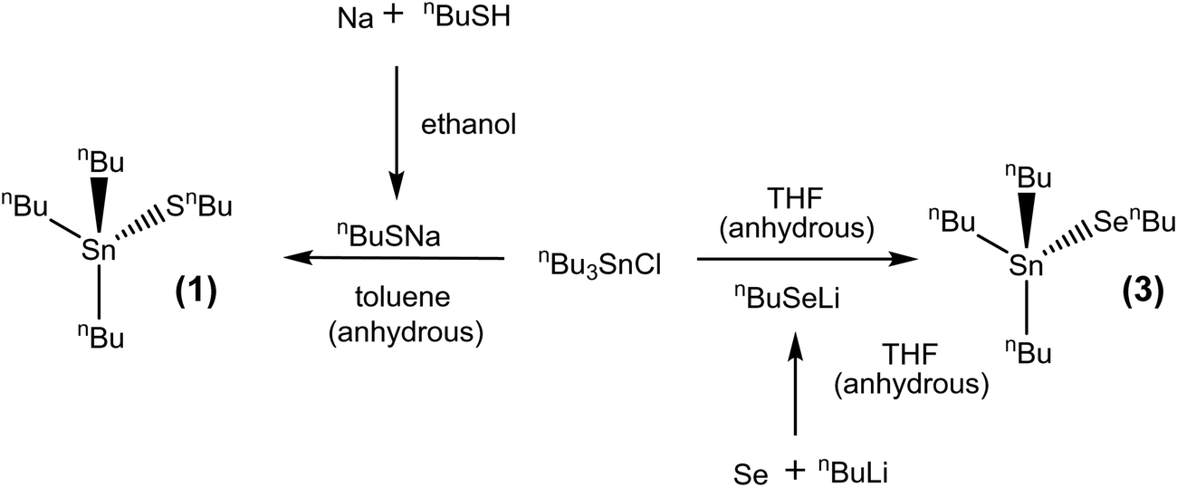 | ||
| Scheme 1 Synthesis of [SnnBu3(EnBu)] (E = S, Se) (1) and (3). | ||
 | ||
| Scheme 2 Synthesis of [SnnBu2(SnBu)2] (2). | ||
The complexes, which were obtained in good yield (70–80%), can be handled in air briefly, but are readily hydrolysed by moisture. They were characterised by multinuclear NMR spectroscopy (1H, 13C{1H}, 77Se{1H} and 119Sn{1H}) (see ESI†) and elemental analysis, as well as by thermogravimetric analysis (TGA) in order to establish the volatilities of the precursors and to guide the temperature range for the low pressure CVD experiments (Fig. 1). The TGA data show that evaporation is almost complete in all cases, with the temperature associated with the onset of evaporation being lowest for precursor (3) at ca. 100 °C, while for (1) and (2) the evaporation onset occurs at ca. 170 °C.
 | ||
| Fig. 1 TGA profiles for (1) (green), (2) (blue) and (3) (red). The TGA experiments were conducted with a temperature ramp rate of 5 °C min−1 and a constant flow of argon gas at a flow rate of 30 mL min−1. | ||
Low pressure CVD experiments
The suitability of the new precursors for the deposition of high quality SnS and SnSe thin films was established via low pressure CVD onto fused silica substrates (8 × 20 × 1 mm3) and resulted in continuous films and good substrate coverage.Depositions from (1) produced sulfur-deficient thin films of SnS, typically containing between 30 and 45% sulfur by EDX analysis. The temperature range for the depositions occurred between 440–530 °C, at pressures between 0.2–0.5 mmHg. Each deposition took 10–12 min (equivalent to the time required for the precursor to fully evaporate).
Precursor (2) was introduced in an attempt to improve the Sn:S ratio towards the target stoichiometric ratio of 1:1, in view of the sulfur-deficiency observed for the films from precursor (1). Depositions using (2) produced stoichiometric SnS in the temperature range 375–490 °C, at a pressure of 0.01 mmHg, with depositions requiring only ca. 3 min once at temperature and with the precursor bulb positioned 2 cm inside the hot zone of the furnace. These depositions used ca. 15 mg of precursor to ensure a short deposition time, hence the films produced were relatively thin (ca. 700 nm), although continuous, with coverage of approximately 1 cm2.
Depositions using 20–40 mg of precursor (3) occurred in the temperature range 350–430 °C (0.01 mmHg), produced stoichiometric SnSe films with continuous coverage over ca. 3 cm2 and required ca. 5–10 min.
Each of the deposited materials was characterised by grazing incidence X-ray diffraction (XRD), scanning electron microscopy (SEM), energy dispersive X-ray spectroscopy (EDX) and Raman spectroscopy. The variable temperature electrical and Seebeck properties have also been explored to evaluate the potential for these thin film materials to be incorporated into TE devices.
Tin sulfide (SnS) thin films
Initial depositions using precursor (1) produced films of highly sulfur-deficient SnS. These films had unusual morphologies, which contained long wires with diameters of ca. 1 μm, as can be seen in Fig. S11 (ESI†). The XRD patterns matched that of SnS and the lattice parameters can be found in the ESI† along with EDX data.The grazing incidence XRD pattern shown in Fig. 2 is from a film grown over ca. 13 min and using 23 mg of precursor (2). The GIXRD pattern shows a single phase SnS in space group Pnma.48 The refined lattice parameters are: a = 11.271(1), b = 4.0134(7) and c = 4.3331(8) Å, in good agreement with the literature values (a = 11.180(6), b = 3.982(2), c = 4.329(3) Å).48
 | ||
| Fig. 2 Top down SEM image (a), cross sectional SEM image (b) and grazing incidence XRD pattern (c) for SnS thin film obtained by low pressure CVD using (2) (red = XRD pattern for bulk SnS48) with a thickness of ca. 6 μm. | ||
EDX analysis (ESI) showed that the thicker films obtained using precursor (2), such as those presented in Fig. 2, were similarly deficient in S as those using precursor (1). However, using a short deposition time of 3 min and a small precursor load, 16 mg, of (2), it was possible to produce samples of SnS thin films that were shown by EDX analysis to contain 49–50% sulfur. The EDX spectrum of one such film is shown in Fig. 3. It is likely that the short deposition time and small amount of precursor reduces the duration that the films are at high temperature under low pressure and minimises loss of the volatile sulfur. The window within which stoichiometric SnS films are obtained via precursor (2) is quite narrow.
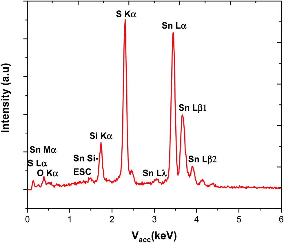 | ||
| Fig. 3 EDX spectrum obtained for a stoichiometric SnS film produced using (2), the Si and O signals are from the underlying substrate. | ||
The grazing incidence XRD pattern of this stoichiometric film (Fig. 4) also shows the SnS in the orthorhombic (Pnma) phase,48 with refined lattice parameters: a = 11.271(1), b = 4.0134(7) and c = 4.3331(8) Å, in good agreement with the literature (a = 11.180(6), b = 3.982(2), c = 4.329(3) Å).48 The XRD pattern suggests a highly orientated, or textured, film. This is the cause of the enhanced intensity of the 201 reflection compared to other peaks and is further corroborated by inspection of the SEM images which clearly show crystallites lying flat and forming interconnected plates across the substrate.
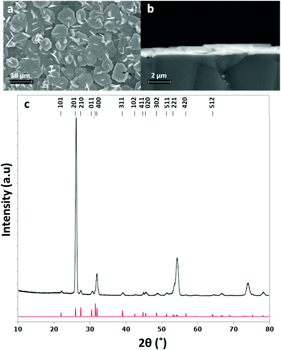 | ||
| Fig. 4 Top down SEM image (a), cross sectional SEM image (b) and grazing incidence XRD pattern (c) for SnS thin film obtained by low pressure CVD using [SnnBu(SnBu)2] (red = XRD pattern for bulk SnS48) with a thickness of around 700 nm. | ||
The Raman spectrum is displayed in Fig. 5. It is consistent with pure SnS, without contamination. The peaks at 98, 190 and 222 cm−1 correspond to the Ag modes, while the 160 cm−1 peak is associated with the B3g mode.49–52 Compared with ref. 51 the peaks are nearly identical in shape, although all shifted by a few wavenumbers. The peak at 222 cm−1 is significantly stronger than in ref. 51 and 52, due to the strong alignment of the film.
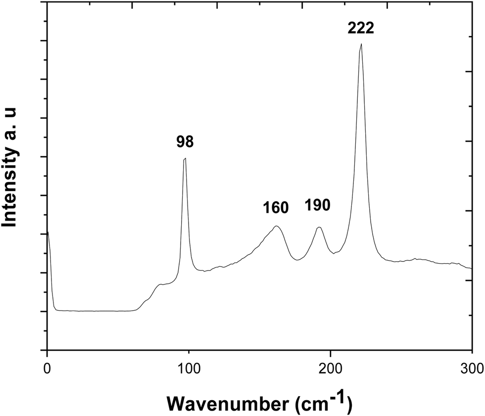 | ||
| Fig. 5 Raman spectrum of the stoichiometric SnS film deposited from precursor (2) with the data highlighting the Ag (98, 190, 222 cm−1) and B3g (160 cm−1) modes. | ||
Tin selenide thin films
The SEM images displayed in Fig. 6 correspond to a thin film of SnSe deposited using precursor (3). The grazing incidence XRD pattern shown in Fig. 6c is in good agreement with the literature data for orthorhombic SnSe (Pnma) and the refined lattice parameters, a = 11.4844(18), b = 4.1555(7) and c = 4.4289(10) Å, are also in good agreement (literature: a = 11.49417(12), b = 4.15096(5) and c = 4.44175(7) Å).53 | ||
| Fig. 6 (a) Top down SEM image of an SnSe deposit, (b) cross sectional SEM image of the same film showing a film thickness of ca. 1.3 μm and (c) grazing incidence XRD pattern for SnSe thin film (black) and the pattern for bulk Pnma SnSe (red).53 | ||
The SEM images of the SnSe film in Fig. 6 show it to be polycrystalline, formed of randomly oriented block-like crystallites, leading to continuous substrate coverage and ca. 1.3 ± 0.2 μm thick. Control over the Sn:Se stoichiometry proved to be much easier than for the tin sulfide films, most likely because of the lower volatility of Se compared to S. EDX analysis of the SnSe films showed that they contained between 48–50% selenium, no impurities evident by EDX analysis (Fig. 7).
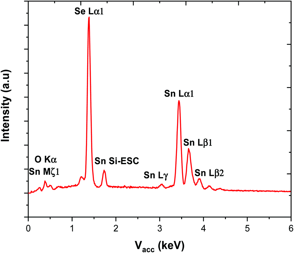 | ||
| Fig. 7 EDX spectrum collected for a thin film of SnSe. | ||
The Raman spectrum of the SnSe film is presented in Fig. 8. This shows peaks at 72, 110, 130 and 152 cm−1, corresponding to the A3g, B3g, A2g, and A3g modes, respectively; the same peaks as in the SnS spectrum. Compared to ref. 51 and 54, the A3g peak is again more intense, most likely due to alignment of the film.54
 | ||
| Fig. 8 Raman spectrum collected for an SnSe thin film with the peaks at 152, 130 and 110 cm−1, corresponding to the A3g, A2g and B3g modes. | ||
Thermoelectric properties
The thermoelectric properties of the stoichiometric SnS film were investigated by temperature dependant Hall and Seebeck measurements, as shown in Fig. 9. The magnitude of the resistance is quite large, but similar to other reported values for polycrystalline SnS (Fig. 9a).7,57 Temperature dependence of the resistivity shows semiconducting behaviour, as also evidenced by the increase in carrier concentration with temperature (Fig. 9b). Mobility in these films is similar to other values reported for polycrystalline SnS.58,59 The decreasing resistivity and decreasing Seebeck coefficient lead to a relatively stable power factor from 0.017 to 0.049 μW cm−1 K−2 at 300 K and 450 K, respectively. | ||
| Fig. 9 Electrical properties SnS thin films. Resistivity (a), Hall mobility and carrier concentration (b), Seebeck coefficient (c), and power factor (d) of the films shown with temperature from 300–450 K. | ||
The thermoelectric properties of the SnSe film were investigated similarly, as shown in Fig. 10. The electrical conductivity of the film increases with increasing temperature, demonstrating a semiconducting, thermally-activated transport behaviour (Fig. 10a). Similar values were also reported by other polycrystalline SnSe thin-films deposited via different techniques.55,56 The relatively low conductivity can be attributed to both low carrier concentration and mobility as displayed in Fig. 10b, which could be strongly linked to the scattering from the grain boundaries as well as the defects induced by the segregation of Sn in polycrystalline SnSe,13 limiting the thermoelectric performance of the SnSe films. Fig. 10c shows large positive Seebeck coefficients, which are well aligned with the low carrier concentrations obtained. Overall, the power factor shows an increasing trend from 0.06 to 0.4 μW cm−1 K−2 at 300 K and 425 K, respectively.
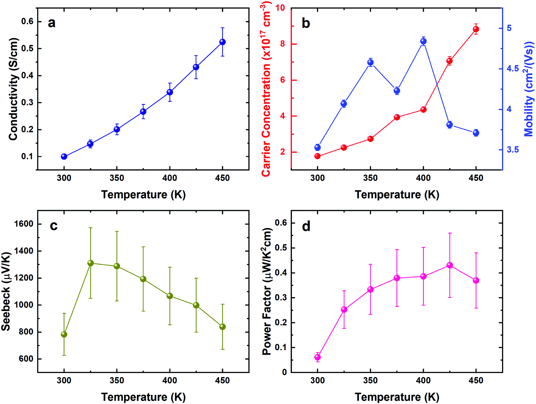 | ||
| Fig. 10 Electrical properties of SnSe thin films. Conductivity (a), Hall mobility and carrier concentration (b), Seebeck coefficient (c), and power factor (d) of the films shown with temperature from 300–450 K. | ||
It is clear that the thermoelectric performance of both undoped SnS and SnSe films are limited by the low carrier concentration and large bandgaps.60,61 Previous pioneering works have shown that these properties can be significantly increased by doping or alloying,62–67 resulting in high ZT values. We have also demonstrated that alloying Bi2Te3 thin films with Bi2Se3 leads to improved thermoelectric behaviour.68 Future work will explore using a similar strategy to further enhance the thermoelectric performances of thin film SnE materials.
Conclusions
Single source precursors suitable for the deposition of stoichiometric thin films of SnS and SnSe have been prepared in high yields and their full spectroscopic characterisation reported. These have been employed successfully using low pressure CVD, giving continuous crystalline, phase-pure thin films of the tin monochalcogenides, as shown by grazing incidence XRD, SEM/EDX and Raman analysis. Variable temperature Seebeck and Hall effect characterisation data show that the films are semiconducting and highly resistive, with the overall power factor for SnS being quite stable with temperature, ranging from 0.017 at 300 K to 0.049 μW cm−1 K−2 at 450 K, while that for SnSe increases from 0.06 at 300 K to 0.4 μW cm−1 K−2 at 425 K.Overall, this provides a promising transferable deposition process with an easily handled precursor system. These results pave the way for future work to optimise the properties further for a range of applications by doping or alloying using this set of compatible molecular precursors bearing n-butyl substituents, while varying the alkyl groups in the precursors can be expected to allow further tuning of their volatility, potentially allowing film growth onto flexible substrates offering good prospects for applications within the realms of energy harvesting.
Conflicts of interest
The authors have no conflicts to declare.Acknowledgements
We thank the EPSRC for a CASE studentship to F. R. (EP/N509747/1) and an iCASE studentship to D. W. N. We also thank Deregallera Ltd and BAE Systems for funding for F. R. and D. W. N., respectively.References
- P. Douglas, ICT – Energy – Concepts Towards Zero – Power Information and Communication Technology, 2014, p. 49 Search PubMed.
- B. Durand, Énergie et environnement: les risques et les enjeux d’une crise annoncée, EDP Sciences, 2007 Search PubMed.
- J. Yan, X. Liao, D. Yan and Y. Chen, J. Microelectromech. Syst., 2018, 27, 1 CAS.
- J. P. Rojas, D. Singh, S. B. Inayat, G. A. T. Sevilla, H. M. Fahad and M. M. Hussain, ECS J. Solid State Sci. Technol., 2017, 6, N3036 CrossRef CAS.
- M. Haras and T. Skotnicki, Nano Energy, 2018, 54, 461 CrossRef CAS.
- B. Z. Sun, Z. Ma, C. He and K. Wu, RSC Adv., 2015, 5, 56382 RSC.
- Y. M. Han, J. Zhao, M. Zhou, X. X. Jiang, H. Q. Leng and L. F. Li, J. Mater. Chem. A, 2015, 3, 4555 RSC.
- L.-D. Zhao, S.-H. Lo, Y. Zhang, H. Sun, G. Tan, C. Uher, C. Wolverton, V. P. Dravid and M. G. Kanatzidis, Nature, 2014, 508, 373 CrossRef CAS PubMed.
- Q. Zhang, B. Liao, Y. Lan, K. Lukas, W. Liu, K. Esfarjani, C. Opeil, D. Broido, G. Chen and Z. Ren, Proc. Natl. Acad. Sci. U. S. A., 2013, 110, 13261 CrossRef CAS PubMed.
- G. Tan, L. D. Zhao, F. Shi, J. W. Doak, S. H. Lo, H. Sun, C. Wolverton, V. P. Dravid, C. Uher and M. G. Kanatzidis, J. Am. Chem. Soc., 2014, 136, 7006 CrossRef CAS PubMed.
- V. P. Vedeneev, S. P. Krivoruchko and E. P. Sabo, Semiconductors, 1998, 32, 241 CrossRef.
- L. Huang, L.-D. Zhao, F. Zhu, H. Yu, Y. Pei, X. Wu, D. He, J.-F. Li, K. Wang, C. Chang, M. Wu, C.-F. Wu, Y. Chen and J. He, Science, 2018, 360, 778 CrossRef PubMed.
- S. Li, X. Li, Z. Ren and Q. Zhang, J. Mater. Chem. A, 2018, 6, 2432 RSC.
- Y. Xiao, C. Chang, Y. Pei, D. Wu, K. Peng, X. Zhou, S. Gong, J. He, Y. Zhang, Z. Zeng and L. D. Zhao, Phys. Rev. B, 2016, 94, 125203 CrossRef.
- I. Y. Ahmet, M. S. Hill, P. R. Raithby and A. L. Johnson, Dalton Trans., 2018, 47, 5031 RSC.
- R. E. Banai, M. W. Horn and J. R. S. Brownson, Sol. Energy Mater. Sol. Cells, 2016, 150, 112 CrossRef CAS.
- D. J. Lewis, P. Kevin, O. Bakr, C. A. Muryn, M. A. Malik and P. O’Brien, Inorg. Chem. Front., 2014, 1, 577 RSC.
- M. Zhang, D. Lei, X. Yu, L. Chen, Q. Li, Y. Wang, T. Wang and G. Cao, J. Mater. Chem., 2012, 22, 23091 RSC.
- L. S. Price, I. P. Parkin, A. M. E. Hardy, R. J. H. Clark, T. G. Hibbert and K. C. Molloy, Chem. Mater., 1999, 11, 1792 CrossRef CAS.
- I. P. Parkin, L. S. Price, T. G. Hibbert and K. C. Molloy, J. Mater. Chem., 2001, 11, 1486 RSC.
- I. S. Chuprakov, K. H. Dahmen, J. J. Schneider and J. Hagen, Chem. Mater., 1998, 10, 3467 CrossRef CAS.
- P. Boudjouk, D. J. Seidler, S. R. Bahr and G. J. McCarthy, Chem. Mater., 1994, 6, 2108 CrossRef CAS.
- P. Boudjouk, M. P. Remington, D. G. Grier, W. Triebold and B. R. Jarabek, Organometallics, 2002, 18, 4534 CrossRef.
- J. Y. Kim and S. M. George, J. Phys. Chem. C, 2010, 114, 17597 CrossRef CAS.
- D. W. Newbrook, S. P. Richards, V. K. Greenacre, A. L. Hector, W. Levason, G. Reid, C. H. K. de Groot and R. Huang, Appl. Energy Mater., 2020, 3, 5840 CrossRef CAS.
- S. L. Benjamin, C. H. de Groot, C. Gurnani, A. L. Hector, R. Huang, E. Koukharenko, W. Levason and G. Reid, J. Mater. Chem. A, 2014, 2, 4865 RSC.
- S. L. Benjamin, C. H. de Groot, A. L. Hector, R. Huang, E. Koukharenko, W. Levason and G. Reid, J. Mater. Chem. C, 2015, 3, 423 RSC.
- G. N. Parsons and R. D. Clark, Chem. Mater., 2020, 32, 4920 CrossRef CAS.
- S. L. Benjamin, C. H. de Groot, C. Gurnani, A. L. Hector, R. Huang, K. Ignatyev, W. Levason, S. J. Pearce, F. Thomas and G. Reid, Chem. Mater., 2013, 25, 4719 CrossRef CAS PubMed.
- C. H. de Groot, C. Gurnani, A. L. Hector, R. Huang, M. Jura, W. Levason and G. Reid, Chem. Mater., 2012, 24, 4442 CrossRef CAS.
- R. Huang, S. L. Benjamin, C. Gurnani, Y. Wang, A. L. Hector, W. Levason, G. Reid and C. H. de Groot, Sci. Rep., 2016, 6, 27593 CrossRef CAS PubMed.
- C. Gurnani, S. L. Hawken, A. L. Hector, R. Huang, M. Jura, W. Levason, J. Perkins, G. Reid and G. B. G. Stenning, Dalton Trans., 2018, 47, 2628 RSC.
- K. Ramasamy, V. L. Kuznetsov, K. Gopal, M. A. Malik, J. Raftery, P. P. Edwards and P. O’Brien, Chem. Mater., 2013, 25, 266 CrossRef CAS.
- M. D. Khan, M. Aamir, M. Sohail, M. Sher, N. Baig, J. Akhtar, M. A. Malik and N. Revaprasadu, Dalton Trans., 2018, 47, 5465 RSC.
- I. P. Parkin, L. S. Price, T. G. Hibbert and K. C. Molloy, J. Mater. Chem., 2001, 11, 1486 RSC.
- B. P. Bade, S. S. Garje, Y. S. Niwate, M. Afzaal and P. O’Brien, Chem. Vap. Deposition, 2008, 14, 292 CrossRef CAS.
- P. Kevin, S. N. Malik, M. A. Malik and P. O’Brien, Chem. Commun., 2014, 50, 14328 RSC.
- I. Y. Ahmet, M. S. Hill, A. L. Johnson and L. M. Peter, Chem. Mater., 2015, 27, 7680 CrossRef CAS.
- A. S. Gordetsov, V. P. Kozyukov, I. A. Vostokov, S. V. Sheludyakova, Y. I. Dergunov and V. F. Mironov, Russ. Chem. Rev., 1982, 51, 485 CrossRef.
- G. Domazetis, R. J. Magee, B. D. James and J. D. Cashion, J. Inorg. Nucl. Chem., 1981, 43, 1351 CrossRef CAS.
- F. Robinson, D. W. Newbrook, P. Curran, C. H. (Kees) de Groot, D. Hardie, A. L. Hector, R. Huang and G. Reid, Dalton Trans., 2021, 50, 998 RSC.
- ICSD: Inorganic Crystal Structure Database (ICSD), Fachinformationszentrum Karlsruhe (FIZ), accessed via the EPSRC funded National Chemical Database Service hosted by the Royal Society of Chemistry.
- S. Graulis, D. Chateigner, R. T. Downs, A. F. T. Yokochi, M. Quirós, L. Lutterotti, E. Manakova, J. Butkus, P. Moeck and A. Le Bail, J. Appl. Crystallogr., 2009, 42, 726 CrossRef PubMed.
- A. J. Gellman, M. T. Buelow, S. C. Street and T. H. Morton, J. Phys. Chem. A, 2000, 104, 2476 CrossRef CAS.
- S. Wang, M. L. McCrea-Hendrick, C. M. Weinstein, C. A. Caputo, E. Hoppe, J. C. Fettinger, M. M. Olmstead and P. P. Power, J. Am. Chem. Soc., 2017, 139, 6596 CrossRef CAS PubMed.
- P. J. Davidson, M. F. Lappert and R. Pearce, Chem. Rev., 1976, 76, 219 CrossRef CAS.
- D. J. Gulliver, E. G. Hope, W. Levason, S. G. Murray, D. M. Potter and G. L. Marshall, J. Chem. Soc., Perkin Trans. 2, 1984, 429 RSC.
- S. Del Bucchia, J. C. Jumas and M. Maurin, Acta Crystallogr., Sect. B: Struct. Crystallogr. Cryst. Chem., 1981, 37, 1903 CrossRef.
- V. R. M. Reddy, S. Gedi, C. Park, R. W. Miles and K. T. R. Reddy, Curr. Appl. Phys., 2015, 15, 588 CrossRef.
- S. Gedi, V. R. M. Reddy, J.-Y. Kang and C.-W. Jeon, Appl. Surf. Sci., 2017, 402, 463 CrossRef CAS.
- L. S. Price, I. P. Parkin, M. N. Field, A. M. E. Hardy, R. J. H. Clark, T. G. Hibbert and K. C. Molloy, J. Mater. Chem., 2000, 10, 527 RSC.
- H. R. Chandrasekhar, R. G. Humphreys, U. Zwick and M. Cardona, Phys. Rev. B: Solid State, 1977, 15, 2177 CrossRef CAS.
- M. Sist, J. Zhang and B. B. Iversen, Acta Crystallogr., Sect. B: Struct. Sci., Cryst. Eng. Mater., 2016, 72, 310 CrossRef CAS PubMed.
- S. Zhou, H. Wang, Y. Zhou, L. Liao, Y. Jiang, X. Yang, G. Chen, M. Lin, Y. Wang, H. Peng and Z. Liu, Nano Res., 2015, 8, 288 CrossRef.
- M. R. Burton, C. A. Boyle, T. Liu, J. McGettrick, I. Nandhakumar, O. Fenwick and M. J. Carnie, ACS Appl. Mater. Interfaces, 2020, 12, 28232 CrossRef CAS PubMed.
- X. Gong, M. Feng, H. Wu, H. Zhou, C. Suen, H. Zou, L. Guo, K. Zhou, S. Chen, J. Dai, G. Wang and X. Zhou, Appl. Surf. Sci., 2021, 535, 147694 CrossRef CAS.
- H. Tang, J. F. Dong, F. H. Sun, Asfandiyar, P. Shang and J. F. Li, Sci. China Mater., 2019, 62, 1005 CrossRef CAS.
- J. Andrade-Arvizu, M. Courel, M. García-Sánchez, R. González, D. Jimenez, I. Becerril-Romero, A. Ramirez and O. Vigil-Galán, Sol. Energy, 2020, 208, 227 CrossRef CAS.
- H. Wu, K. Peng, B. Zhang, X. N. Gong, Z. Z. Feng, X. M. Zhang, M. Xi, X. M. Yan, Y. S. Zhang, G. Y. Wang, X. Lu and X. Y. Zhou, Mater. Today Phys., 2020, 14, 100221 CrossRef.
- R. Guo, X. Wang, Y. Kuang and B. Huang, Phys. Rev. B: Condens. Matter Mater. Phys., 2015, 92, 115202 CrossRef.
- Y. Li, M. Wu, D. K. Song, T. Ding, F. Liu, J. Li, H. Zhang and H. Xie, ACS Appl. Energy Mater., 2020, 3, 6946 CrossRef CAS.
- L. D. Zhao, G. Tan, S. Hao, J. He, Y. Pei, H. Chi, H. Wang, S. Gong, H. Xu, V. P. Dravid, C. Uher, G. J. Snyder, C. Wolverton and M. G. Kanatzidis, Science, 2016, 351, 141 CrossRef CAS PubMed.
- L. D. Zhao, C. Chang, G. Tan and M. G. Kanatzidis, Energy Environ. Sci., 2016, 9, 3044 RSC.
- Z. Wang, D. Wang, Y. Qiu, J. He and L. D. Zhao, J. Alloys Compd., 2019, 789, 485 CrossRef CAS.
- H. Wu, X. Lu, G. Wang, K. Peng, H. Chi, B. Zhang, Y. Chen, C. Li, Y. Yan, L. Guo, C. Uher, X. Zhou and X. Han, Adv. Energy Mater., 2018, 8, 1800087 CrossRef.
- B. Zhou, S. Li, W. Li, J. Li, X. Zhang, S. Lin, Z. Chen and Y. Pei, ACS Appl. Mater. Interfaces, 2017, 9, 34033 CrossRef CAS PubMed.
- Q. Zhao, B. Qin, D. Wang, Y. Qiu and L. D. Zhao, ACS Appl. Energy Mater., 2020, 3, 2049 CrossRef CAS.
- S. L. Benjamin, C. H. de Groot, C. Gurnani, S. L. Hawken, A. L. Hector, R. Huang, M. Jura, W. Levason, E. Reid, G. Reid, S. P. Richards and G. B. G. Stenning, J. Mater. Chem. C, 2018, 6, 7734 RSC.
Footnote |
| † Electronic supplementary information (ESI) available: It includes original NMR spectra for precursors (1)–(3), together with EDX data and additional SEM and XRD data for the S-deficient SnS films deposited using (1). See DOI: 10.1039/d1ma00331c |
| This journal is © The Royal Society of Chemistry 2021 |