
Vibrational and optical identification of GeO2 and GeO single layers: a first-principles study†
Y.
Sozen
a,
M.
Yagmurcukardes
*abc and
H.
Sahin
 *a
*a
aDepartment of Photonics, Izmir Institute of Technology, 35430, Izmir, Turkey
bDepartment of Physics, University of Antwerp, Groenenborgerlaan 171, B-2020 Antwerp, Belgium
cNANOlab Center of Excellence, Groenenborgerlaan 171, B-2020 Antwerp, Belgium
First published on 2nd September 2021
Abstract
In the present work, the identification of two hexagonal phases of germanium oxides (namely GeO2 and GeO) through the vibrational and optical properties is reported using density functional theory calculations. While structural optimizations show that single-layer GeO2 and GeO crystallize in 1T and buckled phases, phonon band dispersions reveal the dynamical stability of each structure. First-order off-resonant Raman spectral predictions demonstrate that each free-standing single-layer possesses characteristic peaks that are representative for the identification of the germanium oxide phase. On the other hand, electronic band dispersion analysis shows the insulating and large-gap semiconducting nature of single-layer GeO2 and GeO, respectively. Moreover, optical absorption, reflectance, and transmittance spectra obtained by means of G0W0-BSE calculations reveal the existence of tightly bound excitons in each phase, displaying strong optical absorption. Furthermore, the excitonic gaps are found to be at deep UV and visible portions of the spectrum, for GeO2 and GeO crystals, with energies of 6.24 and 3.10 eV, respectively. In addition, at the prominent excitonic resonances, single-layers display high reflectivity with a zero transmittance, which is another indication of the strong light–matter interaction inside the crystal medium.
I. Introduction
Over the last decade, semiconducting ultrathin two-dimensional (2D) materials have been extensively studied owing to their promising optical features for nanoscale optoelectronic devices.1–8 Experimental synthesis, theoretical prediction and characterization of novel ultra-thin crystal structures of bulk materials still have critical importance.Germanium dioxide is one of the most studied wide band gap semiconductors possessing a high transparency range and a chemically inert structure. Apart from its amorphous (glassy) structure,9 GeO2 can be found in one of two crystalline forms that distinctly vary with the arrangement of oxygen atoms around the central Ge atom, depending on the environmental conditions. While at room temperature, the thermodynamically stable crystal phase of GeO2 is a tetragonal rutile phase,10 higher temperature values lead to the formation of a metastable α-quartz type trigonal (hexagonal) structure,11,12 and each crystal phase exhibits distinctive vibrational properties, as revealed by the Raman measurements.13,14 The earlier experimental studies demonstrated excitonic absorption of 4.6 eV for r-GeO2,15 which enlarges to 6.6 eV in the case of the α-phase.16 The exciton characteristic in the rutile phase was attributed to direct-forbidden transitions, and this finding was recently supported by a theoretical prediction.17 Further, the α-phase is a piezoelectric material18,19 and displays advanced non-linear optical properties compared to α-SiO2,20,21 while the high-crystalline lattice environment inside the r-GeO2 leads to high thermal conductivity22 and high carrier mobility23 compared to β-Ga2O3. In addition, the α-phase was reported to be suitable to integrate into the surface acoustic wave devices as a substrate.24
Low-dimensional analogues of GeO2 in the form of nanowires,25–27 nanotubes,28 and nanofibers29 were successfully demonstrated experimentally. Besides, the growing interest in 2D van der Waals materials following the discovery of graphene30,31 and its derivatives32–36 also motivated the emergence of demonstrating atomic-scale structures of non-layered GeO2. Recently, Lewandowski et al. demonstrated that the deposition of Ge and O atoms on the Ru(0001) crystal surface constitutes the atomically thin single-layer GeO2 film that presents a hexagonal lattice with a distorted geometry due to the rotation of GeO4 tetrahedron units against each other.37 Furthermore, Zhang et al. suggested a valid experimental methodology to acquire the highly ordered, isolated single-layer sheets of honeycomb structures of several oxide compounds including GeO2.38 It was reported that the layered structures were produced by the oxidation of different metal surfaces in a controlled process manner, and then a single weakly bonded sheet was successfully transferred onto a substrate using stamp-assisted mechanical exfoliation. Although the study presents successful synthesis of ultra-thin oxides, structural phases of the obtained materials remain an open question and should be clarified by future investigations.
Motivated by recent studies, here we focus on the identification of stable hexagonal structures of GeO2 (1T-GeO2) and buckled GeO (b-GeO) single-layers in terms of structural, electronic, vibrational, and optical properties by means of density functional theory (DFT) calculations. Notably, the identification of different phases of germanium oxide can be realized through monitoring their optical and vibrational spectra. The rest of the manuscript is organized as follows: in Section II, we introduce the employed computational methodology; in Section IIIA, we present structural, vibrational, and electronic properties; in Section IIIB, we discuss the optical properties of crystals by means of optical absorption, reflectivity, and transmission spectra; finally, in Section IV, we conclude our results.
II. Computational methodology
In this study, all calculations were performed based on a DFT code within the framework of projector augmented-wave (PAW) datasets39,40 as implemented in the Vienna ab initio simulation package (VASP).41,42 The generalized gradient approximation (GGA) of Perdew–Burke–Ernzerhof (PBE) was considered in order to derive exchange–correlation potential for electronic interactions.43 To compensate for the inability of the GGA functional for the description of accurate dispersion forces, the DFT-D2 method of Grimme was used.44 According to convergence tests performed for each structure, the plane-wave cutoff of 500 eV, and the Brillouin zone sampling with a Γ-centered k-grid of 9 × 9 × 1 were found to be sufficient for structural optimization. In order to get the optimized cell parameters, we maintained the minimization of the ground-state energy until the force on each lattice direction is between ±1 kB. The break criterions for atomic relaxation and electronic self-consistent loop were set to 10−4 eV Å−1 and 10−5 eV, respectively. The continuous network of corresponding crystal structures along the [001] lattice plane was broken by inserting a vacuum gap of 20 Å between the repeated images of single-layers. Types of chemical bonding in crystals were specified by determining the final charge on each atom inside the primitive cell employing Bader analysis.45 For cohesive energy calculations we used the formula given by| ECoh = [nGeEGe + nOEO − ESL]/ntot | (1) |
In order to verify the dynamical stability and investigate the phononic properties of structures, we built the force constant matrix using finite displacement methodology as implemented in the Phonopy package.46 For the phonon band dispersion calculations, 147-atom and 162-atom supercells were considered for 1T-GeO2 and b-GeO single-layers. To acquire the Raman activity of zone-centered phonon vibrations, the derivative of the macroscopic dielectric tensor was taken with respect to the normal mode within the framework of the finite difference method.
In order to estimate optical coefficients by including excitonic effects, quasiparticle eigenvalues were obtained by solving the G0W0 approximation,47–49 which was followed by performing BSE calculation50,51 using quasiparticle wave functions to consider electron–hole interactions. The BSE step was solved with respect to the Tamm–Dancoff approximation. The spin–orbit coupling term was neglected because it has no significant effect on both structures’ electronic states close to the Fermi level, which is enough to cause differentiation in the optical properties. We used 40 Å of vacuum spacing, and 18 × 18 × 1 k-grids in G0W0 and BSE steps to obtain accurate quasiparticle energies (also QP gaps) and excitonic properties. The energy cutoff for the response function was set to 150 eV. The 5 (3) highest occupied and the 5 (3) lowest unoccupied excitonic eigenstates were considered for the 1T-GeO2 (b-GeO) single-layer.
Finally, the acquired real (ε1) and imaginary (ε2) parts of the dielectric function were used to calculate the refractive index (n) and extinction coefficient (κ), with the given formulae
 | (2) |
 | (3) |
 | (4) |
| T(ω) = (1 − R(ω))2e−α(w)l | (5) |
 | (6) |
III. Results
A. Structural, vibrational and electronic properties of monolayers
1T and buckled structures of Ge-based single-layer oxides (namely 1T-GeO2 and b-GeO) are presented in Fig. 1a and 1T-GeO2, and b-GeO consist of three and two atoms in their hexagonal primitive cells, respectively. The octahedral arrangement of O atoms around the central Ge atom leads to the formation of a 1T crystal structure belonging to the P![[3 with combining macron]](https://www.rsc.org/images/entities/char_0033_0304.gif) m2 space group and to the point group of D3d. On the other hand, the crystal lattice of b-GeO consists of vertically separated Ge and O atomic planes. The calculated structural parameters are listed in Table 1. In-plane cell parameters are found to be 2.91 and 3.02 Å for 1T-GeO2 and b-GeO, respectively, with the corresponding Ge–O bond lengths of 1.95 and 2.01 Å. The vertical width of each single-layer, defined as the distance between the outer atomic planes, is found to be 1.97 Å for 1T-GeO2, while it is found to be 1.0 Å for b-GeO. Energetic favorability of each phase is investigated through the cohesive energy of each structure and single-layer 1T-GeO2 is shown to be energetically favorable over b-GeO (with cohesive energies of 5.10 and 4.53 eV per atom, respectively). In contrast, the cohesive energy of 1T-GeO2 is relatively smaller than those estimated for 1T structures of transition metal oxides, such as HfO2 and ZrO2.52 Bader analysis shows that each O atom in single-layer polymorphs tends to receive 1.1 e from Ge atoms, which indicates the highly ionic character of the crystals. The unbalanced charge distribution on the outer planes of b-GeO reveals the induced dipole oriented along the out-of-plane direction. Consequently, the built-in potential difference leads to anisotropy within the out-of-plane work function, which is determined to be 5.62 and 7.11 eV for Ge and O surfaces, respectively, indicating the higher chemical stability of the O-surface. The work function for the 1T phase is calculated to be 8.69 eV, which is higher than that of b-GeO. These values are relatively higher than those reported for the thin films of transition metal oxides, ranging from 3.5 eV (ZrO2) to 7.0 eV (V2O5),53,54 and the traditional monolayers of transition metal dichalcogenides, reported to be 6.11 and 5.89 eV for MoS2 and WS2, respectively.55 Materials that possess high work function values are desirable to be integrated into electronic and optical devices as charge extraction and injection layers that provide improvements in the device ability.56–58
m2 space group and to the point group of D3d. On the other hand, the crystal lattice of b-GeO consists of vertically separated Ge and O atomic planes. The calculated structural parameters are listed in Table 1. In-plane cell parameters are found to be 2.91 and 3.02 Å for 1T-GeO2 and b-GeO, respectively, with the corresponding Ge–O bond lengths of 1.95 and 2.01 Å. The vertical width of each single-layer, defined as the distance between the outer atomic planes, is found to be 1.97 Å for 1T-GeO2, while it is found to be 1.0 Å for b-GeO. Energetic favorability of each phase is investigated through the cohesive energy of each structure and single-layer 1T-GeO2 is shown to be energetically favorable over b-GeO (with cohesive energies of 5.10 and 4.53 eV per atom, respectively). In contrast, the cohesive energy of 1T-GeO2 is relatively smaller than those estimated for 1T structures of transition metal oxides, such as HfO2 and ZrO2.52 Bader analysis shows that each O atom in single-layer polymorphs tends to receive 1.1 e from Ge atoms, which indicates the highly ionic character of the crystals. The unbalanced charge distribution on the outer planes of b-GeO reveals the induced dipole oriented along the out-of-plane direction. Consequently, the built-in potential difference leads to anisotropy within the out-of-plane work function, which is determined to be 5.62 and 7.11 eV for Ge and O surfaces, respectively, indicating the higher chemical stability of the O-surface. The work function for the 1T phase is calculated to be 8.69 eV, which is higher than that of b-GeO. These values are relatively higher than those reported for the thin films of transition metal oxides, ranging from 3.5 eV (ZrO2) to 7.0 eV (V2O5),53,54 and the traditional monolayers of transition metal dichalcogenides, reported to be 6.11 and 5.89 eV for MoS2 and WS2, respectively.55 Materials that possess high work function values are desirable to be integrated into electronic and optical devices as charge extraction and injection layers that provide improvements in the device ability.56–58
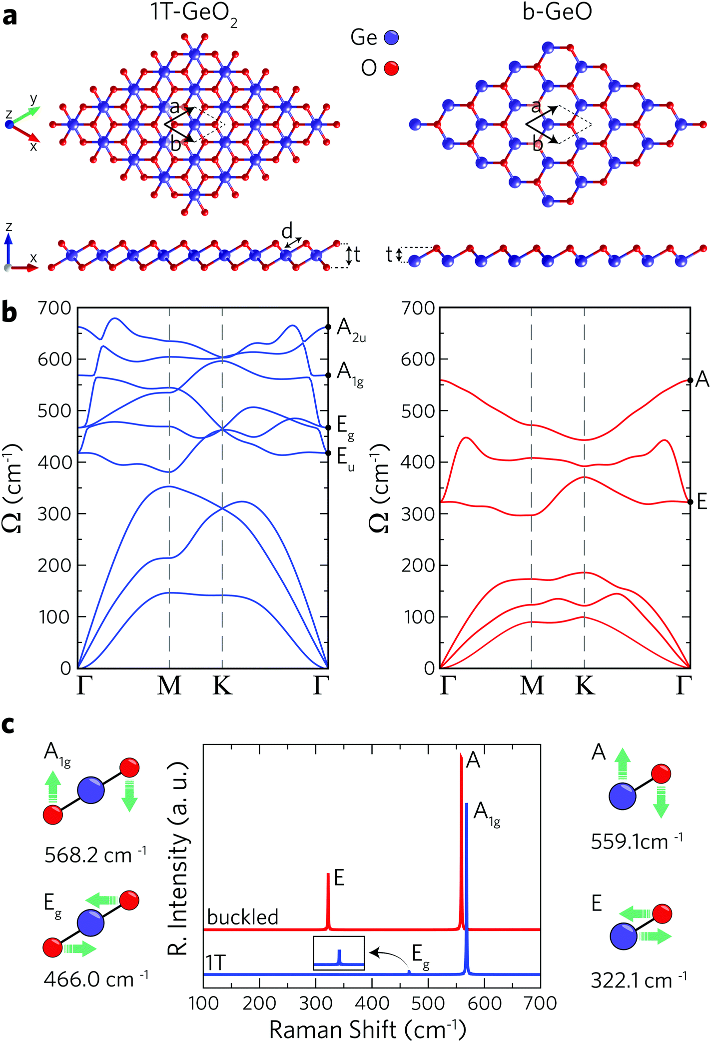 | ||
| Fig. 1 The optimized structures of single-layer 1T-GeO2 and b-GeO. (a) Top and side views (left panel for 1T-GeO2 and right panel for b-GeO), (b) phonon band structures in the same order, and (c) the corresponding Raman activity of zone-centered phonon vibrations. Atomic vibrations of atoms for the four Raman active modes. | ||
| a = b (Å) | d Ge–O (Å) | t (Å) | E Coh (eV) | Δρ, e− | Φ (eV) | E GGAindir (eV) | E GGAdir (eV) | |
|---|---|---|---|---|---|---|---|---|
| 1T-GeO2 | 2.91 | 1.95 | 1.97 | 5.10 | 1.1 | 8.69 | 3.56/KΓ → Γ | 4.04/Γ → Γ |
| b-GeO | 3.02 | 2.01 | 1.0 | 4.53 | 1.1 | 5.62/7.11 | 2.09/K → M | 2.55/M → M |
The phonon band dispersions are calculated in order to confirm the dynamical stability of each free-standing single-layer. In addition, the corresponding Raman spectra are calculated in order to point out the distinctive vibrational features of each structure. According to phonon band dispersions presented in Fig. 1b, the lattice vibrations do not lead to any imaginary frequencies within the BZ revealing the dynamical stability of the structures. Note that the out-of-plane (ZA) acoustic phonon branch of the b-GeO structure displays small negative frequencies around the Γ point. To remove these numerical artifacts we used quadratic curve fitting. Furthermore, the thermal stability of each single layer is investigated by performing molecular dynamics simulations by increasing the temperature from 0 to 300 K for 2 ps, with a time step of 2 fs. These calculations are carried out by considering a 6 × 6 × 1 supercell for each crystal. As a result, we obtain the crystal lattices of single-layers having negligible deformation at room temperature (300 K) (see Fig. S1, ESI†). It is shown that 1T-GeO2 possesses six optical phonon branches that belong to two doubly-degenerate in-plane (Eg and Eu), and two non-degenerate out-of-plane (A2u and A1g) phonon modes. On the other hand, single-layer b-GeO exhibits a doubly-degenerate in-plane and a non-degenerate out-of-plane mode, namely E and A modes. We also perform the zone-centered first-order off-resonant Raman spectrum calculations for each single-layer structure. The atomic vibrations contributing to the Raman active modes are given in Fig. 1c. As shown in the left panel of Fig. 1c, the A1g mode represents the out-of-phase vibration of O atoms in the out-of-plane direction, while the Eg mode arises from the in-plane opposite vibration of O atoms. The wavenumbers of the two modes at the Γ point are found to be 568.2 and 466.0 cm−1, respectively. As shown in the Raman spectrum of 1T-GeO2, the Raman activity of A1g significantly dominates that of Eg. On the other hand, the two Raman active modes of single-layer b-GeO, E and A modes, are attributed to the out-of-phase vibrations of Ge–O pairs along the in-plane and out-of-plane directions, respectively. The two modes are found at frequencies of 322.1 and 559.1 cm−1, respectively. Similar to the case of 1T-GeO2, the Raman activity of the A mode is dominant to that of the E mode. However, the activity ratio of out-of-plane mode to the in-plane one is a distinctive feature for distinguishing the two phases. Note that the activity ratio of A to E in b-GeO is much smaller than that of A1g to Eg in 1T-GeO2. The occurrence of stronger Raman scattering from out-of-plane vibrations compared to in-plane vibrations is the result of the existence of a dipole inside the b-GeO phase. On the contrary, in its derivatives of germanane and silicene where the charge distribution is isotropic on separated atomic planes owing to identical atomic composition, the in-plane phonon modes are reported to display stronger Raman activity.59
The electronic band dispersions of 1T-GeO2 and b-GeO are presented in Fig. 2(a) and (b). The results for both the bare GGA and the G0W0 are shown in the same figure. Note that in this paragraph the results of bare GGA are discussed. It is shown that both single-layer structures exhibit indirect band gap behavior, while the lowest direct band gap energies are also shown. The direct band gap of 1T-GeO2 at the Γ point is calculated to be 4.04 eV, while the favorable indirect band gap energy, whose band edges reside at KΓ/Γ (VBM/CBM), is calculated to be 3.56 eV. On the other hand, the electronic band gap energies are found to be lower for single-layer b-GeO. The direct band gap of b-GeO is at the M point with the energy of 2.55 eV, while the lowest indirect band gap is calculated from the K point to M point resulting in a band gap energy of 2.09 eV.
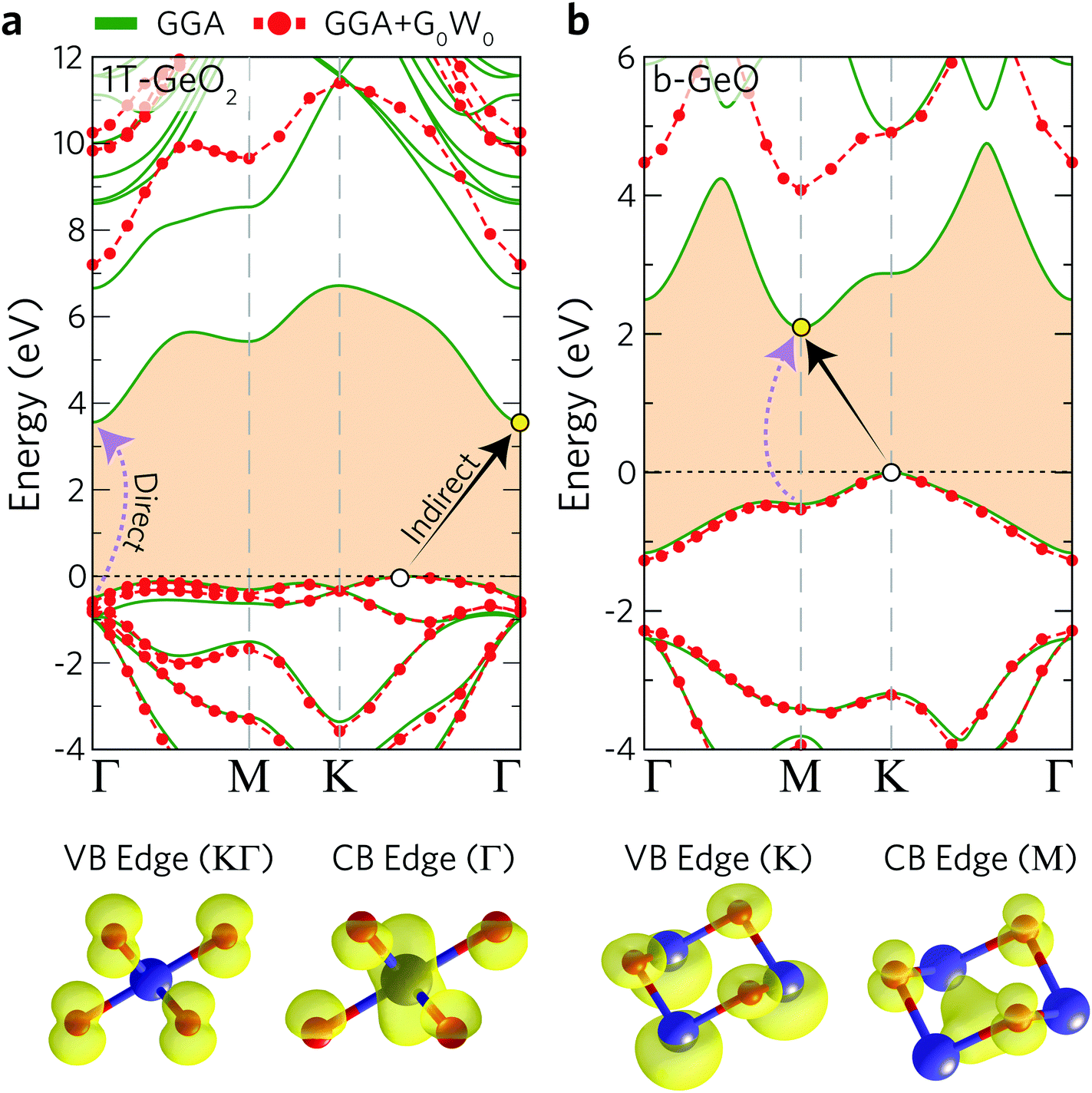 | ||
| Fig. 2 Calculated GGA (green solid) and quasiparticle (GGA + G0W0, red dashed curves) electronic band structures (top panel), and the illustrations of atomic orbitals contributing to the VBM and CBM edges (bottom panel) for (a) 1T-GeO2 and (b) b-GeO single-layers. VBM and CBM edges are marked with white and yellow dots, respectively. | ||
In addition to bare GGA calculations, we also consider many-body effects by implementing the G0W0 approximation to obtain the quasiparticle (QP) band gap of each structure (see Table 2). Our results reveal that the 1T phase displays an ultra-wide indirect band gap indicating its insulating or namely ultra-wide gap semiconducting behavior (gap of 7.20 eV). Moreover, we also investigate the atomic orbital contributions to the VBM and CBM edges and the results are shown in the bottom panel of Fig. 2. It is found that the VBM edge of 1T-GeO2, residing between K–Γ, is dominated by the pz orbitals of O atoms, whereas the CBM edge at the Γ point consists of the s orbitals of Ge and the s orbitals of O atoms. Note that our results for G0W0 agree well with the results reported in the literature (7.07 and 7.55 eV for the indirect and direct band gaps, respectively).60 In the case of single-layer b-GeO, the VBM edge is found to be dominated by the s and px−y orbitals of Ge and O atoms, respectively. In contrast, the CBM edge arises from the contributions of pz orbitals of O atoms, together with the hybridized electron cloud constituted by the py orbitals of Ge atoms. In addition, the electronic band gap energies are found to be 4.08 and 4.61 eV, for the indirect and direct behavior, respectively.
 ; excitonic gap, Eexcgap; exciton binding energy, Ebind
|
|
E excgap (eV) | E bind (eV) | ||
|---|---|---|---|---|
| E indir | E dir | |||
| 1T-GeO2 | 7.20 | 7.79 | 6.24 | 1.55 |
| b-GeO | 4.08 | 4.61 | 3.10 | 1.51 |

B. Optical properties
As a result of the confinement of electrons in the out-of-plane direction, excited charge carriers in 2D materials may display unique behavior differing from their 3D counterparts. The weaker screening effects in atomically thin crystals lead to an increment in the electrostatic interaction between the electron–hole pairs giving rise to excitons with higher binding energies. The exciton binding energy (Ebind) is a measure of the interaction between e–h pairs, important to have information about the type of excitons. Furthermore, it linearly depends on the electronic band gap of the structure.61Optical transitions, reflectance, and transmittance spectra, including electron–hole interactions in single layers, are discussed through calculation of the frequency-dependent complex dielectric function obtained by solving the BSE equation on top of the G0W0 approximation. We consider both in-plane and out-of-plane light polarizations to understand the effect of dipole orientation on the optical response of structures.
The existence of several optical transition levels below the electronic band gap is the fingerprint of the formation of bound excitons inside the single-layers. In 1T-GeO2, the excitonic states appear in the deep UV region of the electromagnetic spectrum giving rise to the formation of tightly bound excitons (see Fig. 3a). The peak at 6.24 eV corresponds to the optical gap of the structure and it arises from the out-of-plane dipole orientation. The in-plane absorption peak with the highest oscillator strength appears at 6.37 eV and indicates the presence of strong excitonic absorption in the crystal. In contrast to in-plane absorption, much weaker out-of-plane absorption is expected because of the enhanced quantum effects in the 2D limit, which lead to the decrease of the strength of dipole oscillations along the direction perpendicular to the sheet normal. Strong excitonic effects, resulting from strong dielectric confinement, are a direct consequence of considerably high Ebind estimated to be 1.55 eV, according to the first exciton level. Notably, its value is greater than those reported for MoS2 and WS2,5,62 while lower than that of h-BN.63,64 Excitons with high binding energies cause an increase in the probability of the radiative recombination process and their bound states are durable against dissociation caused by thermal excitation. Therefore, strongly-bound excitons are desirable in order to achieve high optical quality65 and to produce high-performance exciton-based devices operating at room temperature.66–68 Moreover, the 1T phase exhibits two in-plane excitons that are visible near the indirect fundamental gaps at 6.99 and 7.13 eV.
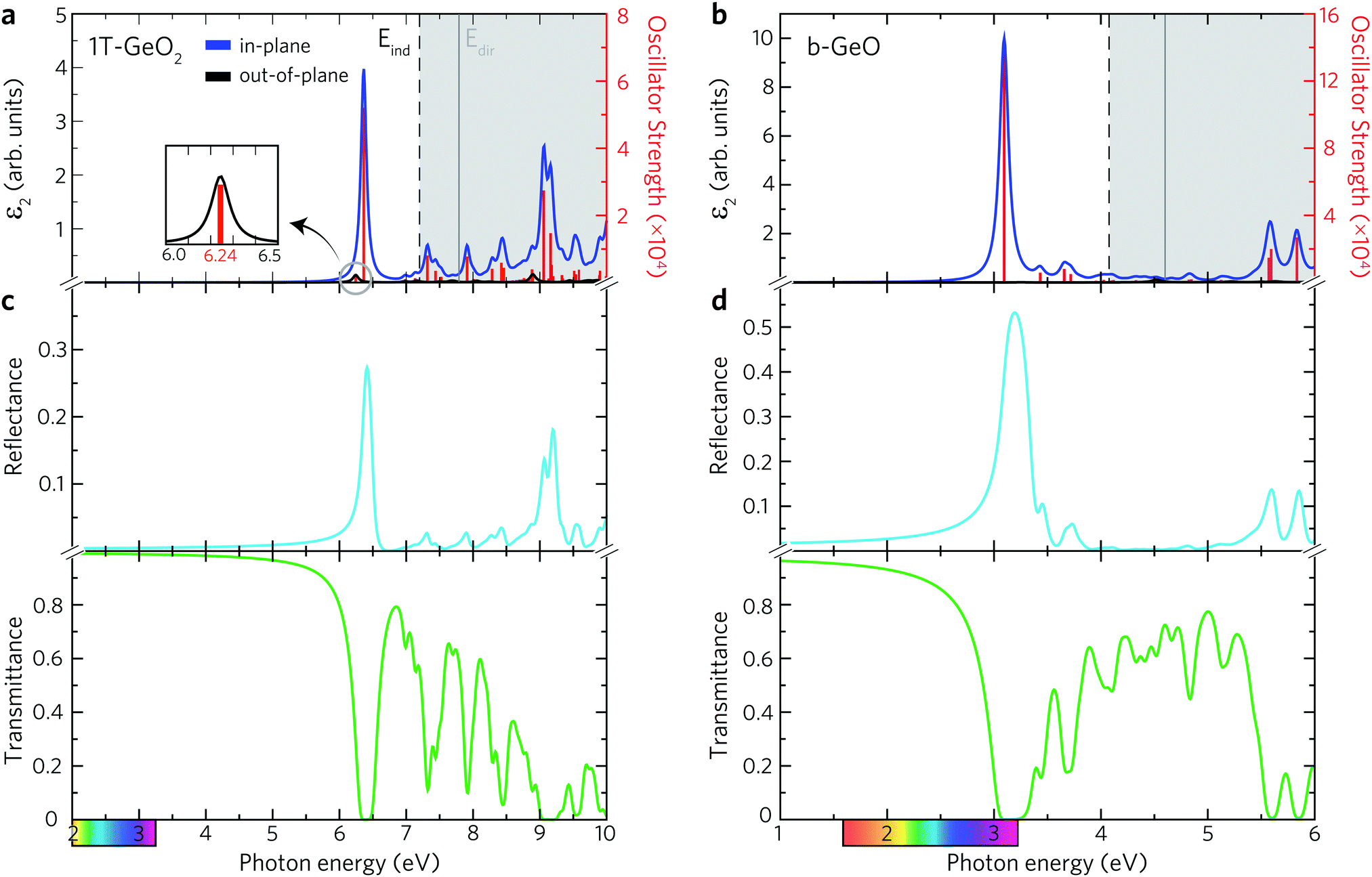 | ||
| Fig. 3 For 1T-GeO2 and b-GeO single-layers, (a and b) the calculated in-plane and out-of-plane components of the imaginary parts of the dielectric functions, (c and d) reflectance, and transmittance spectra, as a function of photon energy. Vertical red lines stand for oscillator strengths of optical transitions, while black dashed and grey solid lines mark the positions of indirect and direct band gaps of the crystals, respectively. | ||
Below the band edge of single-layer b-GeO, four major peaks, which stem from the in-plane excitons, are found to exist, as shown in Fig. 3b. In addition, it is found that there is no contribution from the out-of-plane excitons to the optical spectrum. Owing to the enhanced confinement effects, all the excitonic transitions occur from the in-plane contributions below the band edge. The excitonic absorption edge of the crystal lies at the violet region of the visible light spectrum due to the formed transition state at 3.10 eV with a large oscillator strength. It is almost three times higher in strength than the most prominent peak of the 1T-GeO2. Besides, it possesses a slightly lower Ebind that is estimated to be 1.51 eV. The positions of smaller excitonic responses in the near UV region are found to be at energies of 3.42, 3.66, and 3.72 eV. The strong excitonic features provide evidence for the high photo-responsivity of each single-layer.
The most prominent excitonic peaks of each phase are easily distinguishable within the considered spectral range of the reflectance spectrum, showing a higher reflectivity than the average (see Fig. 3c and d). In the case of 1T-GeO2, the reflection peak, arising from the corresponding exciton, exhibits narrow linewidth with a rate of approximately ∼30%. On the other hand, in the case of b-GeO, reflection from excitonic transition exhibits much greater and broader spectral response with a rate of ∼50%, demonstrating the strong light–matter interaction. The calculated transmittance spectrum reveals that the transmission rate in the 1T-structure resides very close to 100% up to energies of 5 eV. On the contrary, the transmission in b-GeO starts to drop slightly at the beginning of the visible region of the spectrum. In each structure, the light propagation through the crystal environment is totally prevented due to the absorption originating from the dominant exciton state. In short, when the crystal medium interacts with an incident light close to exciton resonance, we only expect the observation of absorption and reflection phenomena. Consequently, it is possible to detect both phases by optical characterizations, thanks to their crystal mediums that are responsive to photon frequencies in different spectral ranges.
IV. Conclusions
In summary, by means of first-principles calculations, we showed that two hexagonal phases of Ge-based oxide single-layers, namely 1T-GeO2 and b-GeO, exhibit distinctive features in terms of their vibrational and optical spectra. Vibrational modes in dynamically stable crystal lattices of 1T-GeO2 and b-GeO lead to Raman wavenumbers in different spectral ranges, as revealed by the first-order Raman calculations. Notably, the Raman activity ratio of out-of-plane/in-plane phonon modes can be used to identify the phase of the Ge–O structure. The employed G0W0 and G0W0 + BSE calculations for the understanding of electronic and optical properties demonstrated that 1T-GeO2 and b-GeO are ultra and wide band gap semiconductors with indirect band gaps, and allow strong excitonic absorption residing at the deep UV and the violet portions of the energy spectrum, respectively. Calculated high exciton binding energies with respect to the lowest transition levels indicate the tightly bound character of excitons in crystals. Furthermore, the reflectance and transmittance spectra are also suitable to monitor the strong light–matter interaction in single-layers due to the high reflection and low transmission values at the vicinity of prominent excitonic absorption. Apparently, the vibrational and optical characteristics of ultra-thin germanium oxide phases can be utilized for their identification.Conflicts of interest
There are no conflicts to declare.Acknowledgements
Computational resources were provided by TUBITAK ULAKBIM, High Performance and Grid Computing Center (TR-Grid e-Infrastructure). H. S. acknowledges support from Türkiye Bilimler Akademisi – Turkish Academy of Sciences under the GEBIP program. M. Y. is supported by the Flemish Science Foundation (FWO-Vl) by a postdoctoral fellowship.References
- Q. H. Wang, K. Kalantar-Zadeh, A. Kis, J. N. Coleman and M. S. Strano, Electronics and optoelectronics of two-dimensional transition metal dichalcogenides, Nat. Nanotechnol., 2012, 7, 699–712 CrossRef CAS PubMed.
- D. Jariwala, V. K. Sangwan, L. J. Lauhon, T. J. Marks and M. C. Hersam, Emerging device applications for semiconducting two-dimensional transition metal dichalcogenides, ACS Nano, 2014, 8, 1102–1120 CrossRef CAS PubMed.
- B. Radisavljevic, M. B. Whitwick and A. Kis, Integrated circuits and logic operations based on single-layer MoS2, ACS Nano, 2011, 5, 9934–9938 CrossRef CAS PubMed.
- K. F. Mak and J. Shan, Photonics and optoelectronics of 2D semiconductor transition metal dichalcogenides, Nat. Photonics, 2016, 10, 216–226 CrossRef CAS.
- A. Ramasubramaniam, Large excitonic effects in monolayers of molybdenum and tungsten dichalcogenides, Phys. Rev. B: Condens. Matter Mater. Phys., 2012, 86, 115409 CrossRef.
- V. Tran, R. Soklaski, Y. Liang and L. Yang, Layer-controlled band gap and anisotropic excitons in few-layer black phosphorus, Phys. Rev. B: Condens. Matter Mater. Phys., 2014, 89, 235319 CrossRef.
- A. Chernikov, T. C. Berkelbach, H. M. Hill, A. Rigosi, Y. Li, O. B. Aslan, D. R. Reichman, M. S. Hybertsen and T. F. Heinz, Exciton binding energy and nonhydrogenic Rydberg series in monolayer WS2, Phys. Rev. B: Condens. Matter Mater. Phys., 2014, 113, 076802 CAS.
- K. He, N. Kumar, L. Zhao, Z. Wang, K. F. Mak, H. Zhao and J. Shan, Tightly bound excitons in monolayer WSE2, Phys. Rev. Lett., 2014, 113, 026803 CrossRef CAS PubMed.
- P. S. Salmon, A. C. Barnes, R. A. Martin and G. J. Cuello, Structure of glassy GeO2, J. Phys.: Condens. Matter, 2007, 19, 415110 CrossRef PubMed.
- W. H. Baur and A. A. Khan, Rutile-type compounds. IV. SiO2, GeO2 and a comparison with other rutile-type structures, Acta Crystallogr., 1971, 27, 2133–2139 CrossRef CAS.
- G. S. Smith and P. B. Isaacs, The crystal structure of quartz-like GeO2, Acta Crystallogr., 1964, 17, 842–846 CrossRef CAS.
- A. W. Laubengayer and D. S. Morton, Germanium. XXXIX. The polymorphism of germanium dioxide, J. Am. Chem. Soc., 1932, 54, 2303–2320 CrossRef CAS.
- J. F. Scott, Raman Spectra of GeO2, Phys. Rev. B: Solid State, 1970, 1, 3488 CrossRef.
- V. V. Atuchin, T. A. Gavrilova, S. A. Gromilov, V. G. Kostrovsky, L. D. Pokrovsky, I. B. Troitskaia, R. Vemuri, G. Carbajal-Franco and C. V. Ramana, Low-temperature chemical synthesis and microstructure analysis of GeO2 crystals with α-quartz structure, Cryst. Growth Des., 2009, 9, 1829–1832 CrossRef CAS.
- M. Stapelbroek and B. D. Evans, Exciton structure in the UV-absorption edge of tetragonal GeO2, Solid State Commun., 1978, 25, 959–962 CrossRef CAS.
- A. N. Trukhin, Luminescence of a self-trapped exciton in GeO2 crystal, Solid State Commun., 1993, 85, 723–728 CrossRef CAS.
- K. A. Mengle, S. Chae and E. Kioupakis, Quasiparticle band structure and optical properties of rutile GeO2 crystal, an ultra-wide-band-gap semiconductor, J. Appl. Phys., 2019, 126, 085703 CrossRef.
- A. Lignie, B. Ménaert, P. Armand, A. Peña, J. Debray and P. Papet, Top seeded solution growth and structural characterizations of α-quartz-like structure GeO2 crystal single crystal, Cryst. Growth Des., 2013, 13, 4220–4225 CrossRef CAS.
- P. Hermet, Piezoelectric response in α-quartz-type GeO2, J. Phys. Chem. C, 2016, 120, 126–132 CrossRef CAS.
- P. Hermet, G. Fraysse, A. Lignie, P. Armand and P. Papet, Density functional theory predictions of the nonlinear optical properties in α-Quartz-type germanium dioxide, J. Phys. Chem. C, 2012, 116, 8692–8698 CrossRef CAS.
- V. Atuchin, B. Kidyarov and I. Troitskaia, Interrelationship of micro-and macrostructure with physical properties of noncentrosymmetric germanates, Ferroelectrics, 2013, 444, 137–143 CrossRef CAS.
- S. Chae, K. A. Mengle, R. Lu, A. Olvera, N. Sanders, J. Lee, P. F. P. Poudeu, J. T. Heron and E. Kioupakis, Thermal conductivity of rutile germanium dioxide, Appl. Phys. Lett., 2020, 117, 102106 CrossRef CAS.
- K. Bushick, K. A. Mengle, S. Chae and E. Kioupakis, Electron and hole mobility of rutile GeO2 from first principles: An ultrawide-bandgap semiconductor for power electronics, Appl. Phys. Lett., 2020, 117, 182104 CrossRef CAS.
- R. Taziev, SAW properties in quartz-like α-GeO2 single crystal, J. Phys.: Conf. Ser., 2018, 1015, 032142 CrossRef.
- X. C. Wu, W. H. Song, B. Zhao, Y. P. Sun and J. J. Du, Preparation and photoluminescence properties of crystalline GeO2 nanowires, Chem. Phys. Lett., 2001, 349, 210–214 CrossRef CAS.
- L. Armelao, F. Heigl, P.-S. G. Kim, R. A. Rosenberg, T. Z. Regier and T.-K. Sham, Visible emission from GeO2 nanowires: site-specific insights via X-ray excited optical luminescence, J. Phys. Chem. C, 2012, 116, 14163–14169 CrossRef CAS.
- Z. Gu, F. Liu, J. Y. Howe, M. P. Paranthaman and Z. Pan, Three-dimensional germanium oxide nanowire networks, Cryst. Growth Des., 2009, 9, 35–39 CrossRef CAS.
- Z. Jiang, T. Xie, G. Wang, X. Yuan, C. Ye, W. Cai, G. Meng, G. Li and L. Zhang, GeO2 nanotubes and nanorods synthesized by vapor phase reactions, Mater. Lett., 2005, 59, 416–419 CrossRef CAS.
- P. Viswanathamurthi, N. Bhattarai, H. Y. Kim, M. S. Khil, D. R. Lee and E.-K. Suh, GeO2 fibers: Preparation, morphology and photoluminescence property, J. Chem. Phys., 2004, 121, 441–445 CrossRef CAS PubMed.
- K. S. Novoselov, D. Jiang, F. Schedin, T. J. Booth, V. V. Khotkevich, S. V. Morozov and A. K. Geim, Two-dimensional atomic crystals, Proc. Natl. Acad. Sci. U. S. A., 2005, 102, 10451–10453 CrossRef CAS PubMed.
- K. S. Novoselov, A. K. Geim, S. V. Morozov, D. Jiang, Y. Zhang, S. V. Dubonos, I. V. Grigorieva and A. A. Firsov, Electric field effect in atomically thin carbon films, Science, 2004, 306, 666–669 CrossRef CAS PubMed.
- M. Xu, T. Liang, M. Shi and H. Chen, Graphene-like two-dimensional materials, Chem. Rev., 2013, 113, 3766–3798 CrossRef CAS PubMed.
- A. Splendiani, L. Sun, Y. Zhang, T. Li, J. Kim, C.-Y. Chim, G. Galli and F. Wang, Emerging photoluminescence in monolayer MoS2, Nano Lett., 2010, 10, 1271–1275 CrossRef CAS PubMed.
- K. K. Kim, A. Hsu, X. Jia, S. M. Kim, Y. Shi, M. Hofmann, D. Nezich, J. F. Rodriguez-Nieva, M. Dresselhaus, T. Palacios and J. Kong, Synthesis of monolayer hexagonal boron nitride on Cu foil using chemical vapor deposition, Nano Lett., 2012, 12, 161–166 CrossRef PubMed.
- M. Yagmurcukardes and F. M. Peeters, Stable single layer of Janus MoSO: Strong out-of-plane piezoelectricity, Phys. Rev. B, 2020, 101, 155205 CrossRef CAS.
- V. Sreepal, et al., Two-dimensional covalent crystals by chemical conversion of thin van der Waals materials, Nano Lett., 2019, 19, 6475–6481 CrossRef CAS PubMed.
- A. L. Lewandowski, P. Schlexer, C. Büchner, E. M. Davis, H. Burrall, K. M. Burson, W.-D. Schneider, M. Heyde, G. Pacchioni and H.-J. Freund, Atomic structure of a metalsupported two-dimensional germania film, Phys. Rev. B, 2018, 97, 115406 CrossRef CAS.
- B. Y. Zhang, K. Xu, Q. Yao, A. Jannat, G. Ren, M. R. Field, X. Wen, C. Zhou, A. Zavabeti and J. Z. Ou, Hexagonal metal oxide monolayers derived from the metal–gas interface, Nat. Mater., 2021, 1–6 Search PubMed.
- G. Kresse and D. Joubert, From ultrasoft pseudopotentials to the projector augmented-wave method, Phys. Rev. B: Condens. Matter Mater. Phys., 1999, 59, 1758 CrossRef CAS.
- P. E. Blöchl, Projector augmented-wave method, Phys. Rev. B: Condens. Matter Mater. Phys., 1994, 50, 17953 CrossRef PubMed.
- G. Kresse and J. Hafner, Ab initio molecular dynamics for liquid metals, Phys. Rev. B: Condens. Matter Mater. Phys., 1993, 47, 558 CrossRef CAS PubMed.
- G. Kresse and J. Furthmüller, Efficient iterative schemes for ab initio total–energy calculations using a plane–wave basis set, Phys. Rev. B: Condens. Matter Mater. Phys., 1996, 54, 11169 CrossRef CAS PubMed.
- J. P. Perdew, K. Burke and M. Ernzerhof, Generalized gradient approximation made simple, Phys. Rev. Lett., 1996, 77, 3865 CrossRef CAS PubMed.
- S. Grimme, Semiempirical GGA-type density functional constructed with a long-range dispersion correction, J. Comput. Chem., 2006, 27, 1787–1799 CrossRef CAS PubMed.
- G. Henkelman, A. Arnaldsson and H. Jónsson, A fast and robust algorithm for Bader decomposition of charge density, Comput. Mater. Sci., 2006, 36, 354–360 CrossRef.
- A. Togo, F. Oba and I. Tanaka, First-principles calculations of the ferroelastic transition between rutile–type and CaCl2-type SiO2 at high pressures, Phys. Rev. B: Condens. Matter Mater. Phys., 2008, 78, 134106 CrossRef.
- L. Hedin, New method for calculating the one–particle Green's function with application to the electron-gas problem, Phys. Rev., 1965, 139, A796 CrossRef.
- M. S. Hybertsen and S. G. Louie, Electron correlation in semiconductors and insulators: Band gaps and quasiparticle energies, Phys. Rev. B: Condens. Matter Mater. Phys., 1986, 34, 5390 CrossRef CAS PubMed.
- M. Shishkin and G. Kresse, Implementation and performance of the frequency-dependent GW method within the PAW framework, Phys. Rev. B: Condens. Matter Mater. Phys., 2006, 74, 035101 CrossRef.
- E. E. Salpeter and H. A. Bethe, A relativistic equation for bound–state problems, Phys. Rev., 1951, 84, 1232 CrossRef.
- W. Hanke and L. J. Sham, Many–particle effects in the optical spectrum of a semiconductor, Phys. Rev. B: Condens. Matter Mater. Phys., 1980, 21, 4656 CrossRef CAS.
- G. Özbal, R. T. Senger, C. Sevik and H. Sevinçli, Ballistic thermoelectric properties of monolayer semiconducting transition metal dichalcogenides and oxides, Phys. Rev. B, 2019, 100, 085415 CrossRef.
- M. T. Greiner, L. Chai, M. G. Helander, W.-M. Tang and Z.-H. Lu, Transition metal oxide work functions: the influence of cation oxidation state and oxygen vacancies, Adv. Funct. Mater., 2012, 22, 4557–4568 CrossRef CAS.
- M. T. Greiner and Z.-H. Lu, Thin-film metal oxides in organic semiconductor devices: their electronic structures, work functions and interfaces, NPG Asia Mater., 2013, 5, e55–e55 CrossRef CAS.
- N. A. Lanzillo, A. J. Simbeck and S. K. Nayak, Strain engineering the work function in monolayer metal dichalcogenides, J. Phys.: Condens. Matter, 2015, 27, 175501 CrossRef PubMed.
- M. Bivour, J. Temmler, H. Steinkemper and M. Hermle, Molybdenum and tungsten oxide: High work function wide band gap contact materials for hole selective contacts of silicon solar cells, Sol. Energy Mater. Sol. Cells, 2015, 142, 34–41 CrossRef CAS.
- P. Schulz, J. O. Tiepelt, J. A. Christians, I. Levine, E. Edri, E. M. Sanehira, G. Hodes, D. Cahen and A. Kahn, High-work-function molybdenum oxide hole extraction contacts in hybrid organic–inorganic perovskite solar cells, ACS Appl. Mater. Interfaces, 2016, 8, 31491–31499 CrossRef CAS PubMed.
- C. Qiu, Z. Xie, H. Chen, M. Wong and H. S. Kwok, Comparative study of metal or oxide capped indium–tin oxide anodes for organic light-emitting diodes, J. Appl. Phys., 2003, 93, 3253–3258 CrossRef CAS.
- M. Yagmurcukardes, C. Bacaksiz, E. Unsal, B. Akbali, R. Senger and H. Sahin, Strain mapping in single-layer two-dimensional crystals via Raman activity, Phys. Rev. B, 2018, 97, 115427 CrossRef CAS.
- F. A. Rasmussen and K. S. Thygesen, Computational 2D materials database: electronic structure of transition-metal dichalcogenides and oxides, J. Phys. Chem. C, 2015, 119, 13169–13183 CrossRef CAS.
- J.-H. Choi, P. Cui, H. Lan and Z. Zhang, Linear scaling of the exciton binding energy versus the band gap of two-dimensional materials, Phys. Rev. Lett., 2015, 115, 066403 CrossRef PubMed.
- H.-P. Komsa and A. V. Krasheninnikov, Effects of confinement and environment on the electronic structure and exciton binding energy of MoS2 from first principles, Phys. Rev. B: Condens. Matter Mater. Phys., 2012, 86, 241201 CrossRef.
- L. Wirtz, A. Marini and A. Rubio, Excitons in boron nitride nanotubes: dimensionality effects, Phys. Rev. Lett., 2006, 96, 126104 CrossRef PubMed.
- R. J. Hunt, B. Monserrat, V. Zólyomi and N. D. Drummond, Diffusion quantum Monte Carlo and GW study of the electronic properties of monolayer and bulk hexagonal boron nitride, Phys. Rev. B, 2020, 101, 205115 CrossRef CAS.
- J. S. Ross, P. Klement, A. M. Jones, N. J. Ghimire, J. Yan, D. G. Mandrus, T. Taniguchi, K. Watanabe, K. Kitamura, W. Yao, D. H. Cobden and X. Xu, Electrically tunable excitonic light-emitting diodes based on monolayer WSe2 p–n junctions, Nat. Nanotechnol., 2014, 9, 268–272 CrossRef CAS PubMed.
- Z. Huang, Y. Liu, K. Dini, Q. Tan, Z. Liu, H. Fang, J. Liu, T. Liew and W. Gao, Robust room temperature valley Hall effect of interlayer excitons, Nano Lett., 2019, 20, 1345–1351 CrossRef PubMed.
- T. Ye, B. Zhou, Z. Liu, Y. Li, H. Shen, C.-Z. Ning and D. Li, Room-Temperature Exciton-Based Optoelectronic Switch, Small, 2021, 17, 2005918 CrossRef CAS PubMed.
- Y. Liu, H. Fang, A. Rasmita, Y. Zhou, J. Li, T. Yu, Q. Xiong, N. Zheludev, J. Liu and W. Gao, Room temperature nanocavity laser with interlayer excitons in 2D heterostructures, Sci. Adv., 2019, 5, eaav4506 CrossRef CAS PubMed.
Footnote |
| † Electronic supplementary information (ESI) available. See DOI: 10.1039/d1cp02299g |
| This journal is © the Owner Societies 2021 |