
Photoelectrochemical water splitting: a road from stable metal oxides to protected thin film solar cells
Carles
Ros
 *a,
Teresa
Andreu
ab and
Joan R.
Morante
ab
*a,
Teresa
Andreu
ab and
Joan R.
Morante
ab
aCatalonia Institute for Energy Research (IREC), Jardins de les Dones de Negre 1, Sant Adrià del Besòs, 08930, Barcelona, Spain. E-mail: cros@irec.cat; Tel: +34 933 562 615
bUniversitat de Barcelona (UB), Martí i Franquès, 1, 08028 Barcelona, Spain
First published on 11th May 2020
Abstract
Photoelectrochemical (PEC) water splitting has attracted great attention during past decades thanks to the possibility to reduce the production costs of hydrogen or other solar fuels, by doing so in a single step and powered by the largest source of renewable energy: the sun. Despite significant efforts to date, the productivities of stable semiconductor materials in contact with the electrolyte are limited, pushing a growing scientific community towards more complex photoelectrode structures. During the last decade, several groups have focused on the strategy of incorporating state of the art photovoltaic absorber materials (such as silicon, III–V compounds and chalcogenide-based thin films). The stability of these devices in harsh acidic or alkaline electrolytes has become a key issue, pushing transparent, conductive and protective layer research. The present review offers a detailed analysis of PEC devices from metal oxide electrodes forming a semiconductor–liquid junction to protected and catalyst-decorated third generation solar cells adapted into photoelectrodes. It consists of a complete overview of PEC systems, from nanoscale design to full device scheme, with a special focus on disruptive advances enhancing efficiency and stability. Fundamental concepts, fabrication techniques and cell schemes are also discussed, and perspectives and challenges for future research are pointed out.
 Carles Ros | Dr Carles Ros Figueras is a postdoctoral research fellow in the Energy Storage and Energy Harvesting group in the Catalan Institute for Energy Research (IREC). Carles completed his bachelor of Physics (2013) and PhD from University of Barcelona (2019) for a thesis on protective layers for stable and efficient photoelectrodes for solar fuels production. His current research focuses on the development of electrodes and photoelectrodes for electrochemical water splitting and CO2 reduction in seawater-based electrolytes as means for energy storage. |
 Teresa Andreu | Dr Teresa Andreu is senior researcher at the Energy Storage group of IREC. She received the degree in Chemistry (1999) and PhD in Materials Science (2004) from the University of Barcelona. After a period in industry and academia, she joined IREC in 2009. Her current research is focused on emerging technologies for hydrogen generation and carbon dioxide conversion (photoelectrochemistry, heterogeneous catalysis and plasma-catalysis), solar fuels and redox flow batteries. She has been part-time lecturer at the materials department at UB (2014–2017) and UPC (2017–2019) and she is the author of more than 100 scientific publications and 4 patents. |
 Joan R. Morante | Professor J. R. Morante is, since 1985, full professor of the Faculty of Physics of the University of Barcelona. Since 2009 he has been the director of the advanced materials for energy of the IREC Institute and since 2015 he were appointed as director. His activities are devoted on energy conversion processes at the nano scale. His efforts are focused on the use of these processes for energy storage and the production of solar fuels, renewable electro/thermos synthesis of fuels and added value chemicals. He has co-authored more than 600 research publications with more than 29.000 citations. |
1. Photoelectrochemical water splitting: introduction
Since the beginning of the industrial revolution, economic growth has been driven by a continuous increase of power consumption,1 which has been possible thanks to the availability, high energy density and low price of fossil fuels. The counter part of its exponential consumption increase has been significant alterations of our planet, some of them irreversible. This global climate change, attributed to anthropogenic greenhouse gas emission to the atmosphere, has risen sea levels and temperatures, causing ecological unbalance and exponential growth of the species extinction rate. In addition, mineral extraction of some specific elements up to the point of scarcity and the consumption of fossil fuels (overcoming the “Peak Oil”, the maximum extraction rate) means the easy and cheap extraction of these is close to coming to an end. Some scientists have considered it a new geological era, the Antropocene, due to the scale of human-caused modifications on Earth's crust and its ecosystems.2Renewable energy sources and energy saving strategies should be implemented globally, which must be favored by new legislations and technological improvements. Wind, solar and other clean energy sources have in common their intermittent energy production and thus, the need of energy storage technologies to balance energy production and consumption. Converting the surplus energy into chemical bonds such as hydrogen gas allows for later usage, grid distribution or long-term storage. With the sun being one of the most abundant energy sources, photoelectrochemical (PEC) water splitting is postulated as one of the most interesting technologies due to worldwide water availability and pollution-free products, enabling hydrogen as a clean energy vector. Currently, most hydrogen gas feedstock is being produced by methane steam reforming, producing CO2 as by-product,3 so clean methodologies are of great impact in this field.
PEC water splitting was discovered in the 70's by Fujishima and Honda,4 where TiO2, an n-type semiconductor material with 3 eV band gap, in contact with an electrolyte, was able to absorb photons and generate enough potential to split the water molecule into hydrogen and oxygen, storing solar energy into chemical bonds, named “solar fuel”.5
Up to the 90's, authors like Bard stated the basis of PEC cells6 and some research works were published with photoactive materials like TiO2 (ref. 7 and 8) or Ni(OH)2 (ref. 9) and semiconductors from the photovoltaic industry such as InP,10 GaP11 or Si,12 although as will be detailed in this review many of them presented minimal stability, productivity or were fabricated with highly expensive materials or techniques. It is comprehensible that PEC water splitting develops simultaneously and with observable interactions with the photovoltaic and catalysis fields, as many fundamental concepts, analysis techniques and advances can be applied indistinctly.
But it not was until 2005 that the interest by the scientific community started a rapid increase, as can be seen in the number of published works containing “photoelectrochemical water splitting” in the Scopus database, from a dozen to up to 875 works being published in 2019. The reader will find in this article that the historical progress of PEC water splitting is quite entangled with the complexity of the devices, in a pursuit for efficient, stable and scalable photoelectrodes.
A PEC device can directly convert solar energy into hydrogen and oxygen (Fig. 1a), although nowadays photovoltaic (PV) cells can be directly coupled to water electrolyzers, such as alkaline electrolysis cells (EC) or proton-exchange-membrane (PEM) electrolyzers,13 both techniques consisting in mature technologies, as presented in Fig. 1b. However, one of the main advantages of PEC is being designed to work at lower current densities, in the range of tens of mA cm−2, reducing electrochemical overpotentials. This results in lower operation voltages in front of commercial electrolyzers, designed to operate with two orders of magnitude higher currents and thus, significantly higher efficiencies are possible.14 Lower current densities enable alternative low cost and earth abundant catalysts to be used. In addition, PEC approach is a simpler architecture, reducing capital investment costs and electrical transportation losses.
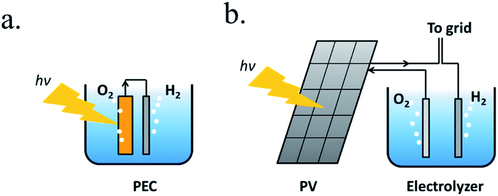 | ||
| Fig. 1 (a) Scheme of a PEC system immersed in the electrolyte, where one of the electrodes is photoactive. (b) Scheme of a photovoltaic panel connected to an electrolyzer with the option to give or take current to the electrical grid. | ||
However, PEC technology has remaining challenges to overcome: as the device will be in direct contact with the electrolyte, corrosion must be avoided, and device configuration is more limited.14 For a large-scale implementation of these technologies, costs must be lower than hydrogen produced by fossil fuels, although environmental regulations and taxes could help in this direction. Nowadays, coupled PV-electrolyzer costs are not expected to reduce significantly, but PEC systems have a lot of possibilities ahead.15,16
The main requirements to achieve competitive PEC water splitting are: (i) absorption of broad part of the solar spectra; (ii) efficient photogenerated electron–hole excitation and separation; (iii) minimized transport losses to the back contact and semiconductor–electrolyte surface; (iv) minimal overpotential on performing the hydrogen evolution reaction (HER) or the oxygen evolution reaction (OER); (v) long term stable operation; (vi) scalable device fabrication techniques; (vii) cost-effective and (viii) earth abundant materials.
The aim of this review article is to show the progress of recent decades' investigations in PEC water splitting with a special attention to the main key parameters to drive PEC technology to be up-scaled: high productivity, long-term stability and cost-effective materials and techniques. Despite been a significant amount of publications in the field, focus has been put on works with disruptive ideas in the path of obtaining high productivity and stability photoelectrodes capable to fulfill market implementation.17 Metal oxides enhancement are reviewed, together with protective strategies for unstable semiconductors capable to generate higher productivities. Finally, cell implementation strategies and configurations are analysed, as well as future prospective challenges for efficient, stable and scalable PEC cells are discussed.
2. Fundamental concepts
Photoelectrochemical water splitting is a complex process, including several phenomena which must be optimized for an efficient device design. In this section, most fundamental ones are explained and depicted in Fig. 2: (a) light-matter interaction; (b) electron–hole pair generation; (c) charge separation and transport; (d) catalytic charge transfer to the electrolyte and (e) the water splitting reaction. As a result of photoelectrochemical water splitting, a current flow (f) is obtained between both electrodes.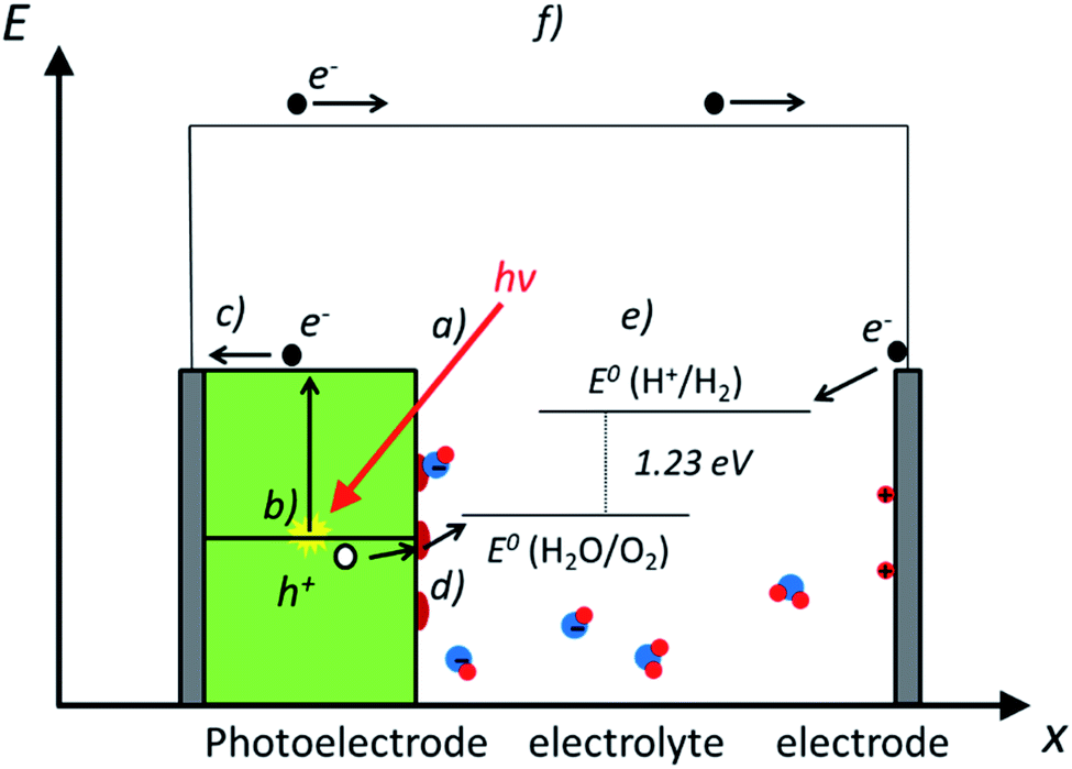 | ||
| Fig. 2 Scheme illustrating the main phenomena involved in photoelectrochemical water splitting, where a photoanode is immersed in an aqueous electrolyte. (a) light-matter interaction, (b) electron–hole pair generation, (c) charge separation and transport, (d) catalysis and (e) the water splitting reaction, and (f) photocurrent associated to the photoelectrochemical (PEC) water splitting. | ||
(a) Light-matter interaction
When light strikes on matter it can be absorbed, reflected or transmitted (Fig. 3a). Across certain media such as liquid electrolytes, light can be slightly absorbed or reflected (scattered), what is considered attenuation. Thus, short propagation distance through the electrolyte is necessary to avoid significant losses. At the interface between two different media with different dielectric constant, a fraction of the incident light can suffer reflection, propagating back in the initial media. Strategies to modulate the divergence between dielectric constants are used in several fields, called “antireflective coatings”, useful to minimize reflection for specific wavelengths ranges. Once inside the material, photons can be absorbed if its energy is higher than the band gap. In this case, photon energy will be transferred to atomic electrons, generating an electron–hole pair. The penetration depth is a measure of how deeply an irradiation can penetrate into a medium. It is defined as the depth at which the photons are absorbed by 1/e (37%), and is an important parameter in thin film semiconductors, as can range from 2 μm for Si (at 555 nm wavelengths) to down to few nanometers for iron oxide. The non-reflected or absorbed light is considered transmitted.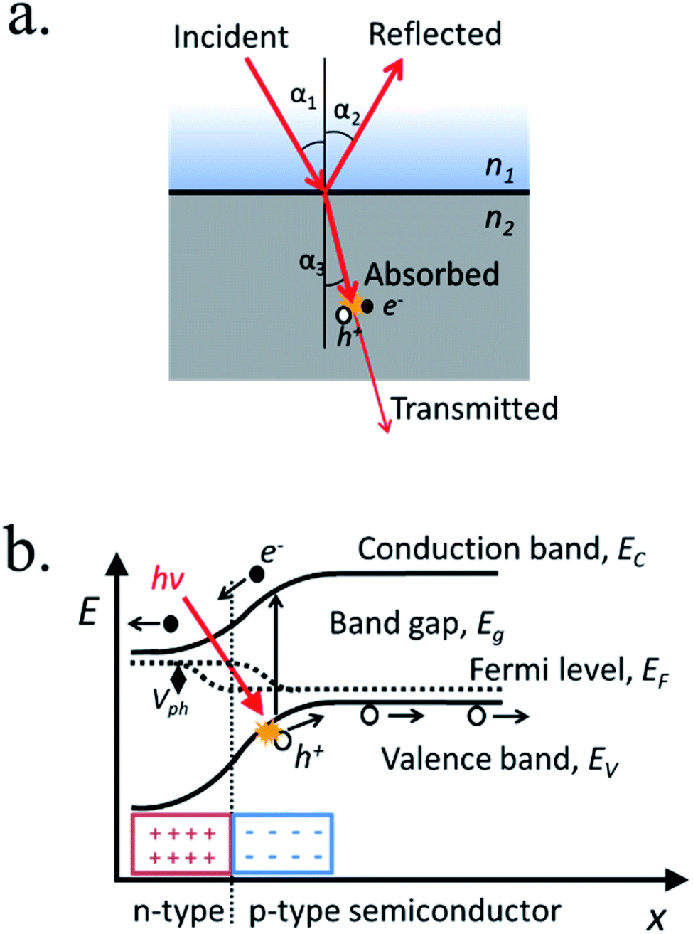 | ||
| Fig. 3 (a) Scheme of a light beam incident on a two different mediums interface with different refractive index, depicting incident, reflected, absorbed and transmitted light and the formation of an electron–hole pair. (b) Energy band diagram of a p–n junction presenting a photon absorbed and the movement of the electron and hole under the built-in electric field, together with the photogenerated voltage between Fermi levels. | ||
(b) Electron–hole pair excitation
If a material absorbs a photon, the energy is transferred to an electron, which is excited to a higher energy level. In a semiconductor's case, electron states from individual atoms have an overall average energy state distribution forming a valence band and a conduction band. At absolute zero temperature, the highest energy occupied states define the valence band edge (Ev) and the lowest energy vacant states define the conduction band edge (Ec), respectively. The energy difference between these two band edges, where no states are present, is the forbidden energy region, named the band gap (Eg).After photon absorption, some of the valence band electrons (e−) are excited into the conduction band leaving an empty state in the network of covalent bonds, considered a “hole” (h+). If photon's energy is larger than the band gap, the electron will dissipate that extra energy (“thermalize”) until stabilizing in the conduction band edge, giving that extra energy to neighbor atoms in the form of thermal vibration and thus, not storing all original photon's energy in the excited electron–hole pair.
For semiconductors at a certain temperature, some of these atoms are spontaneously ionized, where electrons are excited to the conduction band and holes are created in the valence band. The nature of the majority carriers formed, i.e. free electrons or vacancies in the covalent structure, determines the n- or p-type semiconductor behavior. This is normally governed by alterations in the crystal lattice material covalent network, where modifying the amount of acceptors (accepting a free electron) or donors (giving free electrons) is named “doping” the semiconductor, and there are several forms to do it. Among them, the presence of an element with different number of valence electrons (i.e.: a boron atom with 3 electrons in the external shell in a silicon covalent structure consisting on 4-links per atom results in an electron missing in the covalent bonding) or the formation of a sub-stoichiometric material (i.e.: oxygen vacancies in TiO2 are the responsible of n-type semiconductor behavior). The average states distribution energy is called the Fermi level (EF). If Fermi level is closer to the valence band and majority carriers are holes it is considered a p-type semiconductor, and if it is closer to conduction band and electrons are majority carriers, an n-type one.
(c) Charge separation and transport
Light-induced electron hole pairs need to be separated to avoid eventual recombination, the process in which the excited electron releases its energy, “filling” a hole back in the valence band. High recombination rates make impossible to extract any current from photogenerated charges, thus efficient charge separation is needed. Thus, an external potential can be applied, or an internal built-in potential can be used to spontaneously separate photogenerated charges and consequently, to create a photovoltage and a photocurrent. By putting in contact a p-type and an n-type semiconductors a p–n junction is formed, where the average amount of free electrons or holes (Fermi levels) is equilibrated by charges diffusing from one to the other, forming a space-charge or depletion region where there is a strong electric field (Fig. 3b).There are several structures forming built-in electric fields, among them:
- p–n homojunction, where a semiconductor has two regions with different type character (i.e. p-type and n-type silicon).
- p–n heterojunction, where two different materials of different type character are in contact (i.e. n-type TiO2 and p-type silicon).
- Schottky junction, where a semiconductor equilibrates with the free electrons energy level of a metallic film (i.e. Ni metal and n-type silicon).
- A semiconductor–liquid junction (SCLJ), where the semiconductor equilibrates with the ions adsorbed in the surface, forming a Helmholtz double layer (i.e. n-type TiO2 in an alkaline electrolyte).
Formed electric fields will drift generated charges to opposite directions, i.e. electrons to surface and holes to the back contact (Fig. 3b). For efficient charge transport, high conductivity is needed. Conductivity is governed by both carrier mobility and carrier concentration. Carrier mobility highly depends on impurities and defect concentration: electrons and holes highly scatter on crystallographic defects such as interstitial atoms or vacancies, plane dislocations, stacking faults or grain boundaries, losing some energy and changing direction. Meanwhile, carrier concentration is determined by the doping level, temperature and illumination intensity. All these parameters will be reflected in a higher resistance to charge transport.
(d) Catalysis
Once the electrons/holes reach the surface of the photoabsorber, a chemical reaction takes place. In water splitting, the hydrogen or oxygen evolution reaction, respectively. So, not only the charge separation and transport of electrons/holes to the surface is crucial but also, the efficiency of the water splitting reaction and how the electrons are transferred to the reactants to obtain the products. In this sense, catalysts play an important role, accelerating a chemical reaction.An electrocatalyst is defined as a material repeatedly enhancing a certain electrochemical reaction without being consumed. Catalysts introduce alternative reaction paths with lower activation energy through forming alternative intermediate species on its surface. As the reaction will happen on the surface, normally very small amounts of catalysts are needed.
(e) The water splitting reaction
The water splitting reaction| 2H2O → 2H2(g) + O2(g) | (1) |
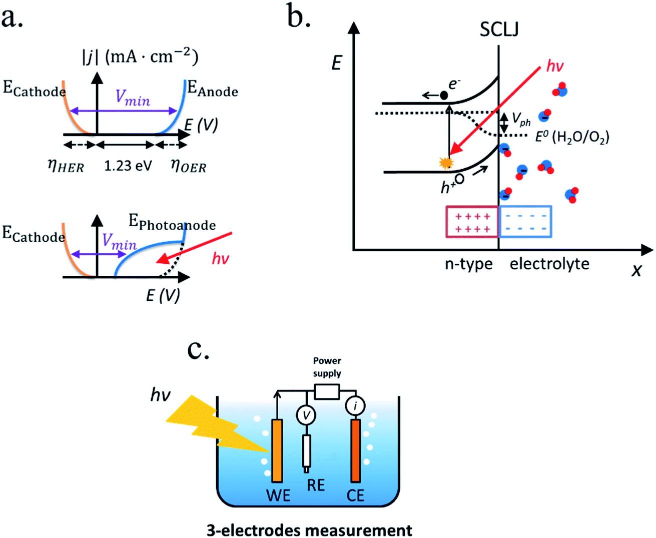 | ||
| Fig. 4 (a) Absolute current versus voltage of the water splitting reaction with the overpotentials for HER and OER depicted (left) and the shape of the water splitting reaction if one of the electrodes is photoactive (right). (b) Energy bands diagram of a photoanode in contact with an alkaline electrolyte, consisting on (left to right) an n-type semiconductor, light-induced electron–hole pair being separated by the space-charge region in the semiconductor–liquid junction (SCLJ), the adsorbed molecules from the electrolyte forming the Helmholtz double layer and the OER redox potential. (c) A 3-electrodes measurement system consisting on a working electrode (WE), a reference electrode (RE), a counter electrode (CE) and a potentiostat measurement system, schematically consisting on a voltmeter, a current meter and a power supply. | ||
HER:
| pH = 0, 4H+ + 4e− → 2H2, E0 = 0 V vs. NHE | (2) |
| pH = 14, 4H2O + 4e− → 2H2 + 4OH−, E0 = −0.83 V vs. NHE | (3) |
OER:
| pH = 0, 2H2O → O2 + 4e−, E0 = 1.23 V vs. NHE | (4) |
| pH = 14, 4OH− → O2 + 2H2O, E0 = 0.4 V vs. NHE | (5) |
Also, to drive these reactions kinetically efficient (with a significant current and thus, productivity), additional potentials are necessary for the catalysis, ηHER and ηOER, named as overpotentials. The overpotential for the water splitting reaction is ∼0.4 V for ∼10 mA cm−2 currents using state of the art catalysts.18–24 The overpotential need to drive the reaction efficiently depends not only on the electrocatalyst nature, but also on the basic or acidic character of the electrolyte, the abundance of hydroxides (OH−) or protons (H+), which plays a key role on the water dissociation kinetics.25 In addition, high ionic conductivity is necessary between the two electrodes, which can introduce another extra potential (ηionic cond.) for large distances or reduced ion concentrations/conductivity, resulting in an ohmic loss. Gases should be separated to avoid back-reactions if they diffuse to the opposite polarized electrode.
Adding all contributions, a minimum required voltage (Vmin) is obtained:
| Vmin(j) = 1.23 eV + ηHER(j) + ηOER(j) + ηionic cond.(j) |
Record values down to ∼1.4 V for a current of around 10 mA cm−2 have been obtained.26,27
(f) Photoelectrochemical (PEC) water splitting
In PEC water splitting, photons absorbed by the semiconductor create electron–hole pairs, which are separated by the built-in electric field inside the photoelectrode, generated in the semiconductor–liquid junction (SCLJ) by semiconductor and electrolyte Fermi level equilibration. A double layer is formed, first described by Helmholtz28 nowadays extended by other authors29 formed by ions physically adsorbed to semiconductor's surface and a diffuse outer layer with exponentially decreasing potential. Electric neutrality is obtained by band bending generated inside the semiconductor.30 The built-in electric field can separate electron–hole pairs, generating photovoltage (Vph) and photocurrent, as depicted in Fig. 4a and b. In a photoanode, holes are driven to photoelectrode's surface to perform the oxygen evolution, meanwhile electrons are collected by the back contact and close the circuit performing the proton reduction reaction in the counter electrode. Similarly, if the semiconductor built-in electric field drives electrons to the surface to perform the hydrogen evolution, it is considered a photocathode. For a significant photocurrent injected into the electrolyte to perform the water splitting reaction, photogenerated electron–hole pairs will suffer overpotentials for charge-separation (ηsep) and for charge transport (ηtrans) across the semiconductor, from the back contact and other elements in the circuit. Some authors have calculated a minimum band gap (Eg min) of the semiconductor material to be >2.04 eV (ref. 30 and 31) based on:| Eg min = ηtrans + ηsep + Vmin |
If the photopotential is generated by a single photoelectrode is not enough, an external bias can be applied to complete the reaction. This way, external power would be used, but it can help in extracting more power from the photoelectrode too.
Independent analysis of each electrode is possible by measuring it in a “three electrodes” cell configuration (or half-cell) (Fig. 4c), where a reference electrode is used (at a fixed potential in respect to the electrolyte). In this disposition, the required current is applied in the counter electrode (CE) by an external power supply (or “potentiostat”) so that between the working electrode (WE) and a reference electrode (RE) there falls the desired potential.32 With this half-cell configuration, the incoming light conversion efficiency into gas given by this single electrode can be measured, named half-cell solar-to-hydrogen (HC-STH) conversion efficiency.

3. Metal oxide photoelectrodes and their enhancement strategies
Metal oxides present several interesting characteristics for PEC compared to other semiconductor materials, such as earth abundance and a relatively large bandgap that results in high photovoltage, required for water splitting. TiO2 was the first studied PEC semiconductor, back in the 70's.4 It is an earth abundant and inexpensive material which has a high stability in alkaline environments and favorable band edge alignment for the OER reaction,34 but for decades obtained photocurrents were far below 1 mA cm−2. This was mainly caused by a 3.2 eV bandgap (absorbing under a 5% of the solar spectrum corresponding to UV light), significant recombination rates and low conductivity due to crystallographic and electronic defects.35To overcome TiO2 limitations, several strategies were applied in following decades:36 alternative metal oxide candidates, band gap modification, nanoscale material structuration, control of electronic defects by new synthesis techniques and post-treatments, surface-decoration with catalysts, creation of heterojunctions, etc. With these modifications, there has been a significant advance of overall productivity and stability.
3.1. Metal oxide photoelectrode candidate materials
Among all possible metal oxides, TiO2 (n-type, 3.2 eV)4,38–42 has been always present as one of the most investigated materials, and other candidates have been widely studied too such as Fe2O3 (n-type, 2.2 eV),43–45 ZnO (n-type, 3.3–3.4 eV),46,47 WO3 (n-type, 2.6–2.8 eV),48–50 BiVO4 (n-type, 2.3–2.5 eV),51–54 NiO (p-type, 3.4 eV)55 and Cu2O (p-type, 2.0 eV).56 More materials have been tested, only some of them with remarkable success, as there are several criteria to be met: corrosion potentials less favorable than HER/OER reactions, proper band alignment for large photovoltage generation, and favorable band position for the desired redox reaction.As it can be observed in Fig. 5, some materials are not useful for water splitting due to unfavorable band alignment, with band edges far from water redox potentials.37 To perform the HER reaction, conduction band must be at more negative potentials relative to NHE than the H+/H2 potential (black dashed line), and for the OER, at more positive potentials than O2/H2O (red dashed line). For a bias-free reaction, both conditions must be met.
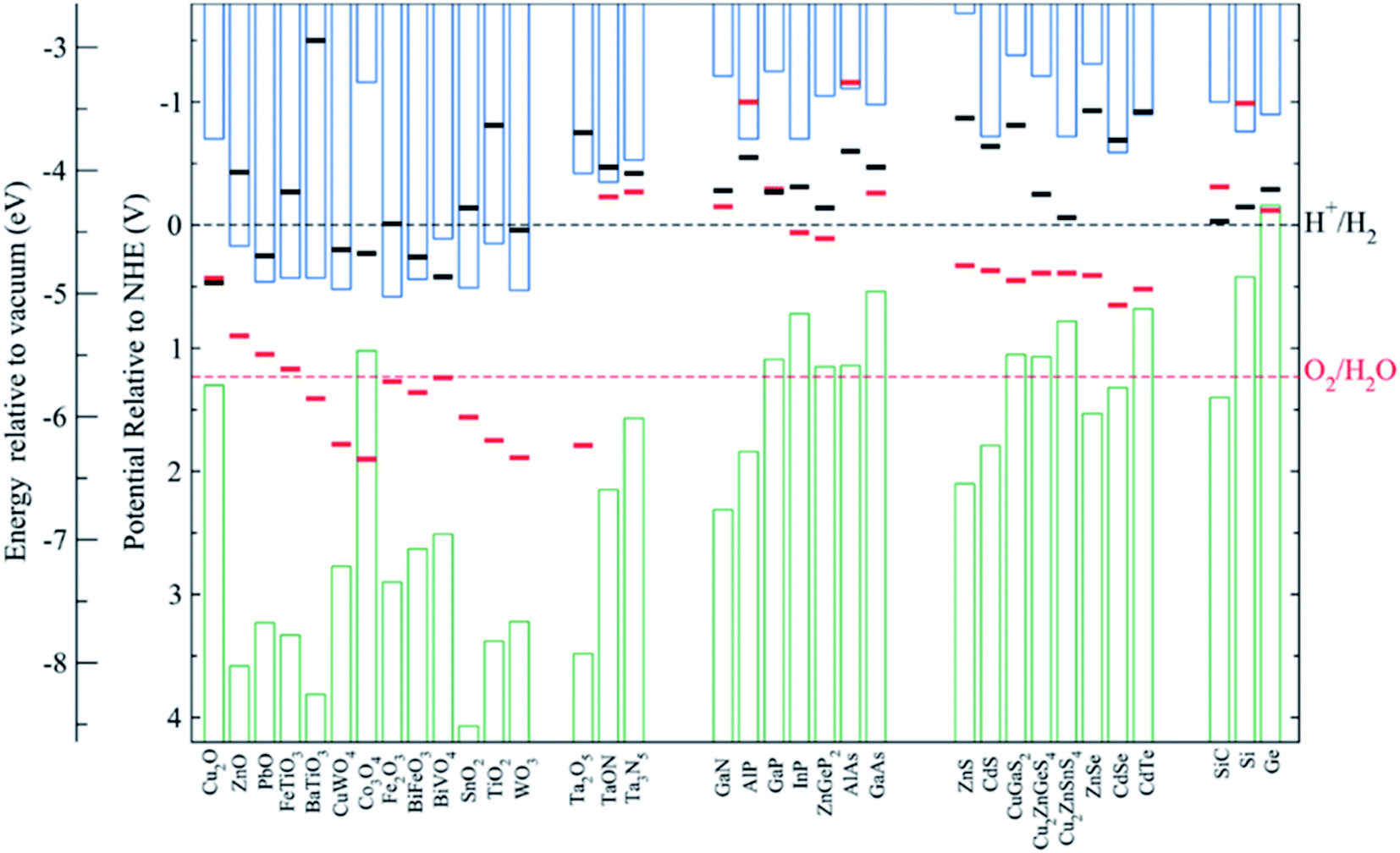 | ||
| Fig. 5 Self-oxidation (red bars) and self-reduction potentials (black bars), and conduction (blue bars) and valence bands (green bars) relative to NHE and vacuum potentials for various semiconductors at pH = 0, 298.15 K and 1 bar. Reprinted with permission from (Chem. Mater., 2012, 24, 3659–3666). Copyright (2012) American Chemical Society.37 | ||
Bard et al.,57 Gerischer et al.58 and other works have discussed in which conditions corrosion reactions are less energetic and thus, thermodynamically more favourable than the HER/OER reaction. S. Chen and L. Wang calculated thermodynamic oxidation and reduction potentials of several semiconductors and compared them to the OER/HER reaction, finding a significant portion of them require protection from corrosion (Fig. 5).37 Generally, a photoelectrode is stable to electron reduction if the self-reduction potentials are more negative relative to NHE than either the H+/H2 or conduction band minimum, and to holes oxidation if self-oxidation potentials are more positive than O2/H2O or valence band maximum.
Some of these oxides, having 3 eV or higher band gaps limit their theoretical maximum current to values lower than 1.8 mA cm−2, such as NiO, TiO2 or ZnO. Alternative interesting candidates in relation to the mentioned parameters are BiVO4, WO3, Fe2O3 and Cu2O, with 2.0–2.5 eV band gaps and theoretical maximum photocurrents over 10 mA cm−2,59,60 but they are prone to crystallographic disorder. They present significant electronic drawbacks: abundant superficial and internal recombination states, low carrier mobility and lifetime. Hence, optimized fabrication of these materials has turned into one of the main investigation fields. As an example, reducing Fe2O3 photoanode thickness or nanostructuring it can overcome the extremely short charge diffusion length and lifetime, reaching up to 4.3 mA cm−2 at 1.23 V vs. RHE, a 34% of its theoretical maximum photocurrent.43 Also, WO3 nanocrystals all grown with a (002) facet orientation have demonstrated to avoid multiple surface energies, and thus, OER overpotentials and kinetics.48
Even expecting high stability, thoughtful investigations have observed chemical and performance degradation by high pH electrolytes in photoanodes such as BiVO4 when protective overlayers or cocatalysts are not used.61 Further increasing materials complexity by multiple metal oxides have shown unprecedented photocurrents up to 2.4 mA cm−2 at 0.4 V vs. RHE for CuFeO2 combined with NiFe/reduced graphene oxide layers.62 The PEC effect based on SCLJ is not limited to oxides. Others such as (oxy)nitrides and nitrides have presented interesting results.63 IrOx–TaON photoanodes64 have shown up to 4 mA cm−2, or CoOx–LaTiO2N nanoparticulate ones65 up to 8.9 mA cm−2 at 1.23 V vs. RHE. Although, much more work is needed in this path, as the amount of possible material combinations and fabrication techniques is enormous.
3.2. Band gap modifications
Large band gap metal oxides have energy band positions prone for water splitting, but lack significant visible light harvesting. Thus, many attempts have been made to modify their bandgap and increase their visible light absorption.66 Creating new states at energies inside the band gap by forming oxygen vacancies or doping with non-metals or transition metals enables smaller energy transitions, thus narrowing the optical band gap. As examples, air annealing67 on TiO2 modifies oxygen vacancies, or nitrogen and hydrogen doping68,69 was performed by Wang et al., giving a yellowish material and enhancing quantum efficiency in the previously inactive energy wavelengths of 450–600 nm. S doping occupies oxygen vacancies and narrows the band gap, achieving visible light absorption,70 among others.71 Although, other works have discarded the decrease of the band gap and attribute the performance enhancement to better charge extraction due to increasing n-type semiconductor behaviour when treating samples in hydrogen reductive atmospheres.72However, these improvements have not reached more than a few % efficiency increase, as creating states inside the band gap also creates detrimental recombination paths for photogenerated electron–hole pairs. Similar studies on bandgap modification by doping have been performed to other materials such as WO3 (ref. 73 and 74) and ZnO.75–77
During recent years increased interest has been put to plasmonic nanocrystals to enhance the absorption of light below band gap energies. TiO2 nanotubes sensitized with ∼1.5 nm glutathione-capped Aux nanoclusters displaying absorption below 525 nm enhanced light absorption for TiO2 photoanodes, significantly under visible light (400–500 nm) excitation.78,79 Zhang et al.80 demonstrated 20 nm gold nanoparticles were capable to increase light absorption in the visible range, but also enhance the UV conversion efficiency. Surface plasmon resonance in these gold crystals is proposed to inject hot electrons to the TiO2 conduction band. They found and increase from 1.22 to 2.25 mA cm−2 at 1.23 V vs. RHE.
3.3. Nanoscale material structuration
Controlling material optical and electronic properties gave metal oxide photoelectrodes a significant push, but optimizing material's morphology by controlling growth process at the nanoscale enabled a completely new field. Nanoscale structuration increases the surface area in contact with the electrolyte, reducing electrochemical kinetic overpotentials by lower current densities. Light absorption and charge transport are also enhanced thanks to decoupling light penetration depth and photogenerated charges diffusion length with nanostructures, facilitating charge transport to the electrolyte by enhanced active surface. Planar devices require thicknesses sufficient to absorb a significant portion of the incident light, and photogenerated charges require diffusion lengths (LD) large enough to reach the electrocatalytic surface and the back contact. In nanostructured devices, the absorption distance for photons is decoupled from the diffusion length of photogenerated charges and thus, allow for higher absorptions meanwhile reducing travel distance for charges, thus reducing current loss (Fig. 6a).81 Moreover, larger active areas in contact with the electrolyte reduce the current density and thus, HER or OER overpotential. 3D structures such as micrometer-size TiO2 anodization,38,69,82–84 rutile TiO2 nanorods hydrothermal growth,72,85–87 WO3 nanowires and nanoflakes,49,88 ZnO nanorods,46,47,76,77 BiVO4 (ref. 51), Cu2O59 and Fe2O3 (ref. 45, 89 and 90) have been fabricated with enhanced PEC performance. | ||
| Fig. 6 (a) Requirements for light absorption and charge diffusion lengths (LD). In nanostructured devices, the absorption distance for photons is decoupled from the diffusion length of photogenerated charges. (b) Glass/FTO substrate microstructuration covered by TiO2 nanorods deposited by hydrothermal. Reprinted with permission from (J. Phys. Chem. C, 2018, 122, 3295–3304). Copyright (2018) American Chemical Society.72 (c) Energy band diagrams of different W doping configurations of BiVO4 photoanodes, enhancing charge separation and transport. Reprinted with permission from (Nat. Commun., 2013, 4, 1–7). Copyright (2013) Springer Nature.106 (d) Overpotentials for 10 mA cm−2 currents of several OER and HER catalysts in acidic and basic electrolytes. Reprinted with permission from (J. Am. Chem. Soc., 2015, 137, 4347–4357). Copyright (2015) American Chemical Society.115 | ||
For instance, Cu–Ti–O nanotube arrays formed by anodization demonstrated increased active surface (tube length, pore and wall thickness) and light absorption by changing the Cu–Ti percentage, giving photocurrents from 0.035 to 0.065 mA cm−2 at −1 V vs. Ag/AgCl in 1![[thin space (1/6-em)]](https://www.rsc.org/images/entities/char_2009.gif) :1 methanol/H2O electrolyte.91 Cu2O nanowires protected with ZnO/TiO2/RuO present increased light absorption and charge separation thanks to nanostrcturation, 5 mA cm−2 for planar and 8 mA cm−2 when nanostructured at 0 V vs. RHE.59,92 By macro-mesoporous optimal structuration, BiVO4 photoanodes obtained photocurrents of 2 mA cm−2 compared with 0.5 mA cm−2 at 1.6 V vs. RHE of the disordered porous films.93 Reducing material thickness can shorten the electrical path for photogenerated charges: i.e., Fe2O3 hematite photoanodes, due to few nanometers carrier diffusion lengths, require nanometer-scale thicknesses to minimize recombination loses.94,95
:1 methanol/H2O electrolyte.91 Cu2O nanowires protected with ZnO/TiO2/RuO present increased light absorption and charge separation thanks to nanostrcturation, 5 mA cm−2 for planar and 8 mA cm−2 when nanostructured at 0 V vs. RHE.59,92 By macro-mesoporous optimal structuration, BiVO4 photoanodes obtained photocurrents of 2 mA cm−2 compared with 0.5 mA cm−2 at 1.6 V vs. RHE of the disordered porous films.93 Reducing material thickness can shorten the electrical path for photogenerated charges: i.e., Fe2O3 hematite photoanodes, due to few nanometers carrier diffusion lengths, require nanometer-scale thicknesses to minimize recombination loses.94,95
Combining substrate structuration and nanoscale material deposition, light absorption and photogenerated charge generation and collection can be improved: i.e. controlling Mo-doped BiVO4 deposition in nanocone-shaped substrates, together with Fe/NiOOH catalyst and appropriate phosphate buffered electrolyte achieved up to 6 mA cm−2 at 1.23 V vs. RHE.96 TiO2-nanorods photoanodes were proven to increase light absorption and thus, photocurrent, when deposited on microstructured glass substrates (Fig. 6b), increasing active area and lateral light incidence to the nanorods.72
3.4. Controlling electronic structure and surface states
To overcome problems such as inefficient charge separation and transport, generating higher and localized potential gradients through electronic doping is key. Metal, hydrogen or nitrogen doping, and oxygen vacancy control have been studied. α-Fe2O3 has been doped with several cations such as Si, Ti, Pt, Cr, and Mo, finding a decrease of the recombination rate by increasing charge transfer and grain-boundary passivation,97–100 or BiVO4 with Li atoms to enhance bulk charge separation.101 CoFe-PBA decoration modified surface states electronic levels enhancing Fe2O3/Fe2TiO5 interfacial charge transfer kinetics.102 Also, partially electrochemical reduction to Fe2O4 (a more conductive phase) can form beneficial conduction paths and reduce recombination.103 BiVO4 has been modified both with W and Mo dopants and by hydrogen treatment to form oxygen vacancies.104 For example, porous BiVO4 can double photoactivity with a 2% Mo incorporation105 and potential gradient can be enhanced by gradual incorporation of W during deposition (Fig. 6c),106 or from 0.3 up to 3.5 mA cm−2 at 1.6 V vs. RHE by hydrogenation at 300 °C thanks to increased donor density, enhancing electron–hole separation and transport.107 BiVO4 Fermi level has been shown to rise while water exposure due to superficial oxygen decreasing, partially reducing BiVO4.108 TiO2 electronic band structure has also been intensively studied, where the depletion region was optimized in nanorod structures by vacancy formation with thermal treatments under ammonia87 or hydrogen72 atmosphere, increasing its photocurrent up to 1.2 mA cm−2 at 1.23 V vs. RHE.Also, minimizing superficial electronic states, when acting as trap states, is interesting to reduce photogenerated electron–hole recombination and thus, enhancing PEC efficiency. This can be achieved controlling the synthesis and post-treatments, and incorporating other metals on the surface to fill the traps and to act as OER catalysts. Fe2O3 photoanodes surface recombination can be reduced by CoOx,109 Ga2O3 (ref. 109 and 110) or TiO2 (ref. 111) surface states passivation. TiO2 surface recombination rate was lowered by removing detrimental chlorine atoms (blocking oxygen evolution active sites) by a 250 °C annealing treatment,85 or by increasing hydroxyl groups acting as hole trap sites after ammonia treatments.87 Depositing atomically-thin films covering the surface is also a very effective strategy to supress detrimental superficial states, avoiding recombination paths and contributing to shifts in the band positions of the metal oxide photoelectrode respect to the electrolyte, enhancing obtained potentials.112,113 Optimal post-fabrication temperature and atmosphere annealing control has a key role in many metal oxides such as α-Fe2O3, where morphology, Sn doping, and introduction of oxygen vacancies, enhances significantly the performance in a low oxygen annealing atmosphere.114
3.5. Surface decoration with cocatalysts
Photoelectrodes such as Fe2O3, CuO2 or TiO2 have suitable surface states to directly perform the desired reaction, but the use cocatalysts can enhance their performance thanks to favourable superficial energetics, improving reaction kinetics. Examples of these catalysts are Pt, MoS2 or RuOx for the HER reaction and Ni/FeOOH, CoPi or IrOx for the OER (Fig. 6d).19,35,116–118 Some of these cocatalysts are noble metals (Pt, Ru, Ir, …), scarce and expensive for large-scale deployment, what has pushed investigation in earth-abundant alternative efficient electrocatalysts.21,115,119In the HER case, photocathodes such as Cu2O have been decorated with Pt (best performing HER catalyst) and RuOx,59 and also earth abundant MoS2 cocatalysts.20,115 Tilley et al. used RuOx or Pt as catalysts and an AZO/TiO2 protective layer (also forming an heterojunction) to obtain over 0.55 V vs. RHE onset potential and 5 mA cm−2 photocurrents for Cu2O photocathodes.120 Amorphous MoS2 allowed earth-abundant Cu2O for up to 5.7 mA cm−2 at 0 V vs. RHE at pH 1.121
OER reaction is a complex four electron process, with slow kinetics in most of the surfaces.95 Enhancing reaction kinetics or reducing potential barriers thanks to cocatalysts have improved the performance of TiO2 and Fe2O3 photoanodes.122 For example, hierarchically nanostructured TiO2 photoanodes decorated with Au particles doubled photocurrent up to 2 mA cm−2 at 1.23 V vs. RHE;123 or α-Fe2O3 ones obtained up to 15% current increase and over 200 mV cathodic shift with Cobalt phosphate (Co-Pi) electrocatalyst.124 Co-Pi also improved BiVO4 photoanodes performance up to 1.7 mA cm−2,53,105 and FeOOH catalyst incorporation in a 0.1 M KH2PO4 + 0.1 M Na2SO3 electrolyte, increased BiVO4 anodic photocurrent to 2.0 mA cm−2 at 1.23 vs. RHE.52
3.6. Metal oxide heterojunctions
Up to now, improvement strategies for single metal oxides have been analysed, but the combination of different metal oxides opens a whole field of opportunities. By the introduction of other materials layers or substrates, charge separation can be improved by forming heterojunctions.For photoanodes, several authors have studied the WO3/BiVO4 heterojunction, obtaining up to 4 mA cm−2 at 1.23 V vs. RHE, almost doubling productivity obtained by each oxide separately.88,125 The band energy difference of the two materials enhances charge separation, and different band gaps allow for increased light absorption. Also, covering a BiVO4 photoanode with ZnFe2O4 overlayer increased its photocurrent and decreased the onset potential, helped in making it resistant to alkaline electrolytes, sustaining 3 mA cm−2 at 1.23 V vs. RHE.51
For photocathodes, Cu2O was covered with an AZO/TiO2/Pt multilayer grown by atomic layer deposition (ALD), obtaining stable and up to 2 mA cm−2 photocurrents at 0 V vs. RHE.92 Similar structures but on Cu2O nanowires and with RuOx as catalyst increased the photocurrent up to 8 mA cm−2 at 0 V vs. RHE, almost the double than the same Cu2O/AZO/TiO2/RuOx structure on planar photoelectrodes.59
Other works have used 3D nanostructuration combined with heterojunction formation with different bandgap materials used to create core–shell structures to obtain the best of each part. For example, porous WO3 layers grown on top of Si microwires have been deposited, enhancing light absorption and photogenerated charge collection and transport (Fig. 7a).126–128 Liu et al. demonstrated a Z-scheme photoelectrode depositing TiO2 nanorods on the top of Si microwires, making each of the tree-like structures a bias-free photoelectrode.129 TiO2 nanorods on top of Si microwires combine large and small bandgap materials too (Fig. 7b and c),129,130 although much work is still needed to overcome interfacial detrimental charge recombination paths. The strategy to use small band gap semiconductors such as Si opens a completely new field of scheme possibilities, increased productivities and new challenges, which will be discussed in following sections.
 | ||
| Fig. 7 (a) Scheme of an np+-Si/WO3 tandem structure including an ITO film in-between forming an ohmic contact (left) and its corresponding band diagram (right). Reprinted with permission from (Energy Environ. Sci., 2014, 7, 779). Copyright (2014) Royal Society of Chemistry.126 (b) SEM image of TiO2 nanorods grown on n-Si microwires to form an heterojunction and its corresponding band diagram. Reprinted with permission from (Energy Environ. Sci., 2014, 7, 779). Copyright (2014) Royal Society of Chemistry.130 (c) Fully integrated tandem structure with the top part of Si microwires covered by TiO2 nanorods and bottom part not, forming a “tree” tandem structure. Reprinted with permission from (Nano Lett., 2013, 13, 2989–2992). Copyright (2013) American Chemical Society.129 | ||
3.7 Overall metal oxide enhancement
As has been reviewed over Section 3, there are several strategies to enhance the performance of metal oxide photoelectrodes, and the best performing works are those using several of them in a synergistic way. For photocurrents over 2 mA cm−2 band gaps shorter than 3 eV are mandatory, material selection is key. Band gap modification was demonstrated possible, although with reduced photocurrent increase together with the introduction of significant recombination rates. Increasing the absorption for energies below band gap with plasmonic surface resonance has presented disruptive results and more work will be needed in this field. Meanwhile, heterojunction formation with different materials opens an enormous amount of possibilities to put together the best characteristics of different materials and to increase the maximum photovoltage and photocurrent.Nanoscale structuration of the photoelectrode into nanowires, nanorods or other structures has enhanced some low charge mobility materials such as TiO2 and Fe2O3 thanks to reducing diffusion length of photogenerated charges together with increased active area. This nanostructuration is only interesting if highly ordered crystalline structures are generated, with high charge mobility and ordered surfaces. An increased defective surface could simultaneously enhance open bonds and electronic states at the surface, increasing the recombination rate. The best results using nanoststructuration have been the ones where the photoelectrodes are synthesized with techniques such as hydrothermal growth, capable to fabricate highly ordered crystalline nanostructures.
Finally, catalyst incorporation has revealed to be key if significant currents are to be obtained. Metal oxide surfaces have been demonstrated favourable for the OER reaction but, if photocurrents are to be increased at least up to 10 mA cm−2, efficient kinetics are also necessary and this has only possible with some materials as presented in Fig. 6b.
The work of Luo et al., with Cu2O nanowires wrapped by AZO, TiO2, and RuOx layers, is a good example on how combining nanostructuration, synthesis optimization, multilayer heterojunction and cocatalyst decoration makes it possible to approach the theoretical maximum photocurrent of 14 mA cm−2.59 These extra layers also protected the Cu2O photoabsorber from corrosion, as it would reduce to metallic Cu due to monovalent copper oxide having the redox potentials within the bandgap.92
4. Short band gap semiconductors for PEC water splitting
In the previous section, strategies to overcome the main drawbacks presented by metal oxide photoelectrodes for water splitting were discussed. The successful candidates and modification strategies capable of obtaining photocurrents higher than 8 mA cm−2 with significant photovoltages are very few. In parallel to PEC water splitting development, the photovoltaic field (PV) science and industry has optimized photoabsorbers and fabrication techniques up to commercial devices with minimal recombination and transport losses. PV productivities have been based on short band gap materials (1–1.5 eV) capable of absorbing the majority of visible spectrum, with materials achieving large carrier mobility thanks to minimized defects and disorder.131–134 Monocrystalline silicon-based solar cells, giving photocurrents over 40 mA cm−2 and 700 mV open circuit photovoltages are nowadays largely dominating the market thanks to relatively cheap price and material abundance, several years operation stability and efficiencies over 22%. Monocrystalline silicon has not been the only photoabsorber commercialized: polycrystalline and amorphous silicon, together with CdTe, GaAs and CIS/CIGS have been already commercialized, and other semiconductors such as perovskites or CZTSSe are emerging rapidly (Fig. 8).131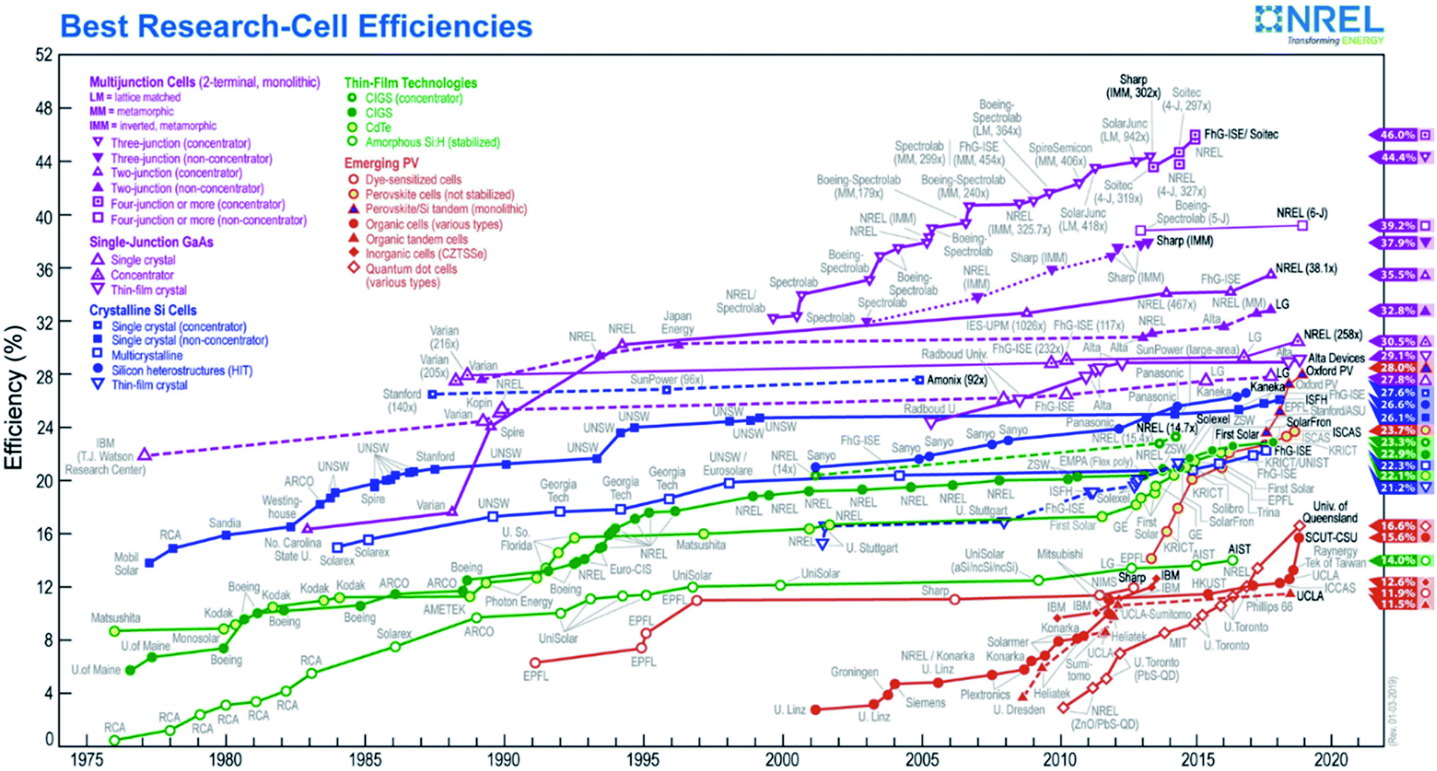 | ||
| Fig. 8 2019 plot of highest-recorded photovoltaic efficiency by year of various photovoltaic devices classified by technology (colours). Prepared by the National Renewable Energy Laboratory (NREL, http://www.nrel.gov). | ||
During the last decade, implementing short band gap materials in PEC water splitting has attracted much interest, thanks to all the knowledge and development from PV industry and thus, the possibility to obtain significantly higher outputs than with metal oxides. Although, the use of these photoabsorbers presents extra challenges added to the photovoltaic ones. Not having a large band gap, and thus photovoltage, will require a tandem structure combining ∼1.1 and 1.6–1.8 eV semiconductors photovoltages or an external bias to use all of their capacity, as it will be reviewed in Section 8.2, tandem PEC devices. Moreover, monolithic photoelectrodes must be immersed in the electrolyte, preferably in acidic or alkaline electrolytes where the electrochemical activity is highly enhanced. But these electrolytes are normally corrosive for most of the presented photovoltaic materials. Strategies to overcome these instabilities must be found to enable these materials for PEC water splitting.
4.1. Fundamentals of materials corrosion
In PEC devices, years-long photoabsorber sustained activity will be necessary for cost-effective devices, thus materials facing the electrolyte have to be thermodynamically stable in the selected electrolyte or extremely low corrosion kinetics must be involved, as discussed in Section 3.1.Some possible corrosion mechanisms can be material dissolution into the electrolyte, superficial insulator layer formation, or chemical detrimental modifications of the photoabsorber, all of them capable of disabling PEC activity. Pourbaix diagrams, where the electrochemical stability for different redox states of an element as a function of pH is plotted, present a first approximation to predict the theoretical thermodynamic stability of a certain material in an aqueous environment.138 They provide data if there will be a state of oxidation change (i.e. passivation) and/or a phase change (i.e. dissolution) of a certain material when varying the applied potential or electrolyte's pH. Some examples are presented in Fig. 9. If complex nanostructures are used as catalytic surfaces, their corrosion (chemical and mechanical) must also be taken in account.139
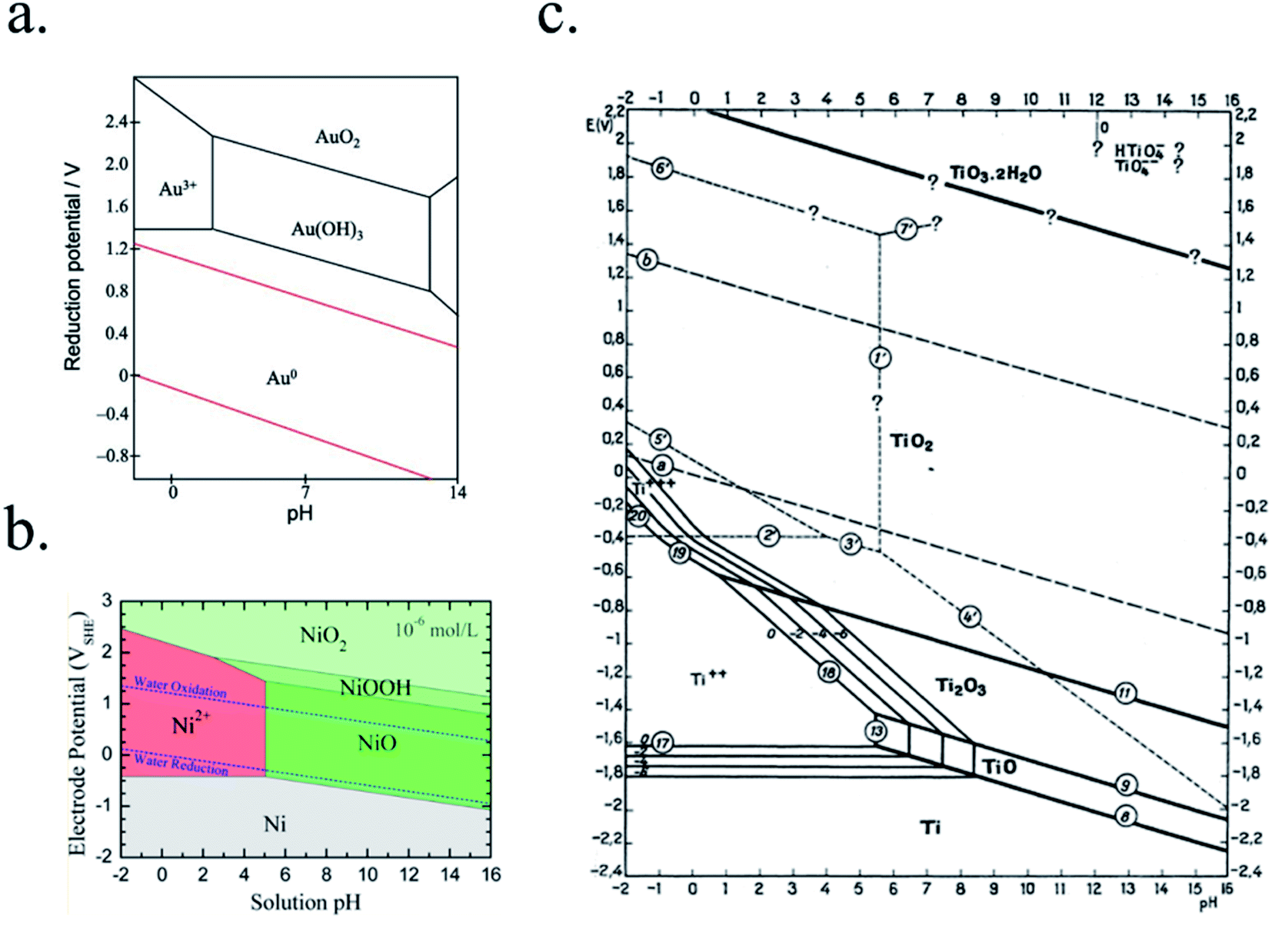 | ||
| Fig. 9 Examples of Pourbaix diagrams of (a) gold (reproduced from Huayhuas-Chipana et al.135) (b) nickel (reprinted with permission from (J. Phys. Chem. C, 2017, 121, 9782–9789). Copyright (2017) American Chemical Society.136) and (c) titanium in aqueous electrolytes (reprinted with permission from Parsons137 copyright (2017) J. Electroanal. Chem. Interfacial Electrochem.). | ||
4.2. Small band gap semiconductors corrosion examples in aqueous electrolytes
Each material is affected by corrosion in different ways, depending on most favourable reaction governed by pH or applied potentials, so it must be analysed in its specific conditions. For example, silicon, by far the most used PV photoabsorber, has been reported to corrode through different processes depending on the used electrolyte.140–144 Both in HER or OER potentials, silicon stability will depend on pH, being oxidation in acidic or dissolution in alkaline. The self-limited passivation reaction of Si forming a thin SiO2 layer in acidic electrolytes (pH ∼ 0),145 a transparent but highly insulator layer, will eventually stop charge injection into the water splitting reaction. Whereas, formed SiO2 dissolves in alkaline electrolytes (pH ∼ 14) and will continuously etch the photoelectrode forming recombination paths for photogenerated charges or even dissolving the p–n junction, rapidly losing photocurrent.140,141,145 Thus, in acidic electrolytes self-limited SiO2 formation in pinholes will not significantly affect overall performance if the rest of the surface is protected,146 but in alkaline electrolytes will not stop etching the silicon beneath, and thus, eventually fatal for the photoelectrode.145Regarding other PV cells based on photoabsorbers such as cadmium-telluride (CdTe), copper-indium/gallium-selenide (CIS/CIGS/CGS) or its earth-abundant alternative, copper-zinc-tin-sulphide/selenide (CZTS/Se), their own structure is based on a multiple materials stack, also containing transparent conductive oxides (TCO, like In:SnO2 (ITO) or Al:ZnO (AZO)) and n-type CdS, forming the p–n junction. ZnO147,148 and SnO2 (ref. 147, 149 and 150) are not stable in highly acidic or alkaline electrolytes or reductive potentials, as they form soluble species.147,150 Regarding CdS151–153 and also CdTe,154 Cd dissolves in highly acidic and alkaline electrolytes,155 and is thermodynamically stable only at significant cathodic overpotentials, not attained without applied bias. Cu-based photoabsorber (CIS, CIGS, CZTS, …) are complex multielement films, highly electronically sensible to vacancies, and would be significantly degraded in contact with electrolytes, although losing the p–n junction with CdS is the main degradation factor.
Among other emerging photovoltaic materials,131 there is none expected to be highly stable for PEC applications under direct contact with the electrolyte. Cells fabricated with silicon, no matter if it is monocrystalline, polycrystalline, HIT, amorphous or micro/nanocystalline156 will suffer from dissolution or passivation when exposed to alkaline or acidic electrolytes, respectively, as discussed previously. Perovskites, a highly promising PV material, have a main drawback: significant degradation under humidity,157 what would require extra encapsulation efforts, especially if put to work in contact with aqueous electrolytes, although some works have fabricated perovskite-based photoelectrodes158 with special efforts in protecting them.159 Organic solar cells have been implemented in PEC160 but require careful selection of redox couples, limiting their efficiency and pointing in stability problems. Dye sensitized solar cells (DSSC) or Grätzel cells, molecular dye decoration of a MOx framework as an intermediate to OER/HER catalyst presents significant instability of the molecular dye in the used potentials and electrolytes ranges. Thus, low productivities are expected,161 or full cell encapsulation would be required, then further connected to the electrolyte with an external circuit, forming a PV-EC device configuration.162
5. Protective layers to implement photovoltaic photoabsorbers into water splitting
Several strategies are possible to implement highly active photoabsorber materials into PEC water splitting avoiding their corrosion. Some authors have functionalized the surface of semiconductors with organic reagents like two-step chlorination/alkylation163 or by an alkylation through the halogenation/Grignard route164 to suppress corrosion, with relative success, but the majority of efforts have been put on depositing inorganic layers onto the photoabsorber to separate it from direct contact with the electrolyte.112,165 Protective ultrathin layers of any material must consider even very slow dissolution rates (chemical or mechanical) for long-term operating devices, especially when considering flow systems and direct contact with gas bubbling.These protective layers must allow electrical conduction, be thermodynamically stable, and optically transparent. M. F. Lichterman et al. stated all the properties under the acronym “SABOR”, meaning “![[S with combining low line]](https://www.rsc.org/images/entities/char_0053_0332.gif) table in the thermodynamic, kinetic, and mechanical senses when incorporated onto the semiconductor, immersed in the electrolyte, and operated at the potentials of interest;
table in the thermodynamic, kinetic, and mechanical senses when incorporated onto the semiconductor, immersed in the electrolyte, and operated at the potentials of interest; ![[A with combining low line]](https://www.rsc.org/images/entities/char_0041_0332.gif) ctive catalytically for the OER/HER, either possessing intrinsic catalytic activity or integrating the activity of a co-catalyst; capable of providing
ctive catalytically for the OER/HER, either possessing intrinsic catalytic activity or integrating the activity of a co-catalyst; capable of providing ![[B with combining low line]](https://www.rsc.org/images/entities/char_0042_0332.gif) uilt-in electronic asymmetry to allow for the separation of electrons and holes, or to allow for a separate buried junction to perform efficiently;
uilt-in electronic asymmetry to allow for the separation of electrons and holes, or to allow for a separate buried junction to perform efficiently; ![[O with combining low line]](https://www.rsc.org/images/entities/char_004f_0332.gif) ptically transparent to provide optical properties that are optimized for the transmission of light; and, capable of providing low
ptically transparent to provide optical properties that are optimized for the transmission of light; and, capable of providing low ![[R with combining low line]](https://www.rsc.org/images/entities/char_0052_0332.gif) esistance, to allow for charge-carrier conduction with minimal performance loss due to iR drops”.166
esistance, to allow for charge-carrier conduction with minimal performance loss due to iR drops”.166
With protective layers incorporation, device complexity increases but photovoltage will now be governed by a solid-state junction rather than by the photoabsorber–electrolyte junction, increasing the possible materials candidates to be used. The extra layer can either form an heterojunction, or protect a buried junction. In addition, if the protective layer is not catalytic, an extra catalyst (layer or particles) must be added to reduce overpotentials. Although several interesting heterojunction strategies have been demonstrated for PEC water splitting electrodes with more or less success, focus will be put on extracting maximum efficiency from the photoabsorbers, using these extra layers to protect the photovoltaic-like junctions and the different techniques to deposit them.
5.1. Thin film deposition techniques
Thin film technology has become one of the main fields of study last decades, from basic sciences to industrial processes. Controlling material deposition at the nanoscale opens a whole new world of possibilities by combining physical and chemical properties from single or multiple element materials with overcoming intrinsic limitations due to phenomena only happening at the nanoscale.167 For example, titanium dioxide, a wide band gap metal oxide, considered insulator at the macroscale, is conductive at the nanoscale; or metals, highly visible-light reflective and absorptive, can be turned into transparent if deposited few nanometers thick. There are a large amount of deposition techniques and variations among them for diverse applications, but some of the most used ones for inorganic thin film protective layers have been selected.There are many non-vacuum liquid and chemical-based thin film deposition techniques, but not all of them are used to synthesize protective layers for different reasons. Among the liquid-based thin film deposition techniques, dip coating, spin coating or chemical bath deposition (CBD)168 are the more used ones, but require direct contact of the photoabsorber with a liquid, what might alter its superficial chemical state and thus, performance. In addition, liquid-based techniques normally produce either porous, not homogeneous at the nanoscale or abundant-pinhole films compared to vacuum technologies, and to eliminate precursor residues or crystallize them they require thermal post-treatments, which can create cracks in the protective layer or affect the photoabsorber. For example, solution-deposited TiO2 by spin-casting or spray pyrolysis presented significant pinholes, allowing electrolyte to penetrate and dissolve the photoabsorber, being fatal for the device even with 80 nm thick layers.169
Electroplating is one of the oldest techniques to form metallic thin films since the 19th century. Generally known as electrochemical deposition,170 a conductive substrate (in our case, the photoabsorber) is introduced in an electrolyte containing the desired thin film precursor ions and, under controlled polarization, a redox reaction occurs, forming a film of electrodeposited material in the surface of the electrode (Fig. 10a). It can be extended to any material capable to be deposited in a certain potential window that will depend on the electrolyte media, and is very interesting thanks to its easiness and the wide range of materials possible to be deposited, from metals to metal oxides and sulphides, even with nanoscale morphology control. It requires no vacuum, usually it is carried out at room or moderate temperatures, and with affordable infrastructure, like a power supply, lab equipment and the precursor materials. As drawbacks, it is highly depending on the substrate, that needs to be conductive, and has a moderate throwing power (the capacity to deposit an uniform film over an irregular substrate), not suitable for nanostructured substrates where a high aspect ratio is required. In some cases, nucleation promote the formation of particles rather than a layer, such as electrodeposited Ni oxide/hydroxide, a transparent, chemically resistant and catalytic material, that forms porous layers,23,171 not isolating the substrate from electrolyte, whereas NiO deposited by sputtering creates a solid impermeable layer.172 Also, the substrate will be in direct contact with the electrolyte and its properties can be affected. Many works have used electrochemical techniques to deposit catalytic particles or films to enhance OER or HER kinetics on already previously protected semiconductors.173
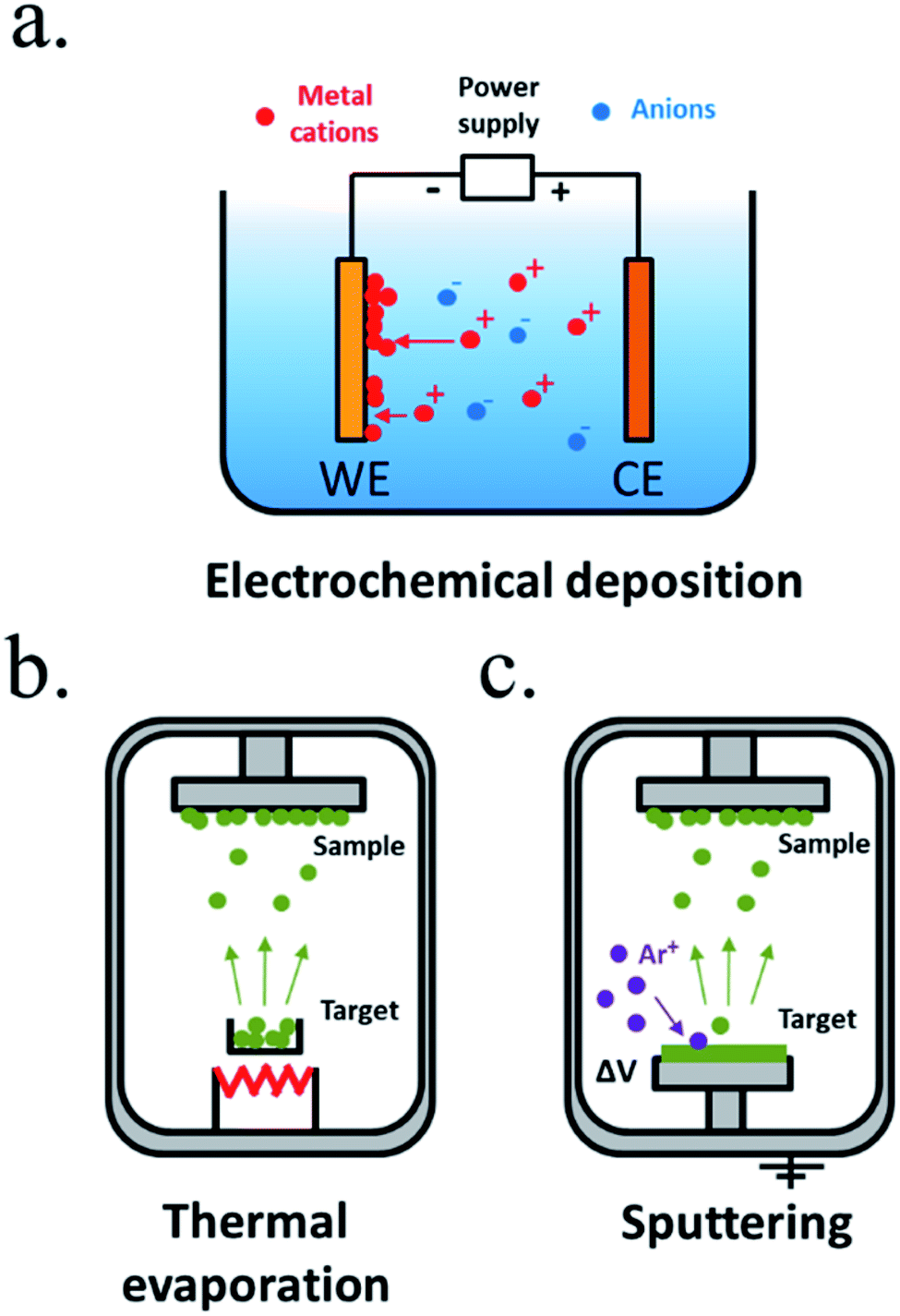 | ||
| Fig. 10 Representative schemes of thin film deposition techniques by (a) electrochemical deposition, (b) thermal evaporation and (c) sputtering. | ||
Vacuum technologies allow for an inert and controlled atmosphere deposition, favourable for more homogeneous deposited films and process-control.168 Among the physical vapour deposition (PVD) techniques, thermal evaporation is one of the simplest, where a crucible is heated to high temperatures, vaporizing the materials contained.168,174 Evaporated particles will travel and solidify forming a film on top of a substrate (Fig. 10b). However, as different elements vaporize at different temperatures, the technique is useful for single element metals but has reduced stoichiometry reproducibility for mixes elements. Evaporated metallic films have been used as intermediate, protective or catalytic layers in water splitting. Sputtering deposition175,176 is based on an inert gas (i.e. argon) being ionized and accelerated towards a blank, impacting with high energies and removing particles which will travel until being deposited in our substrate (Fig. 10c). Direct current (DC) sputtering is useful for conductive blanks (materials to be deposited), and radio-frequency (RF) sputtering allows insulator materials deposition. In reactive sputtering, other gases can be introduced at low pressures in the chamber, reacting with the traveling particles before being deposited (i.e. the oxygen presence can be controlled to tune metal oxides stoichiometry and with this, electrical, optical or other characteristics). Sputtering has been widely used to deposit catalysts177 and protective layers, thanks to the material possibilities, among them stoichiometry-controlled oxides such as TiO2 (ref. 178 and 179) or NiO172 and no dependence on used substrate. Some authors have required layers such as 8 nm Ti to prevent damaging sensible photoabsorbers such as amorphous Si during the sputtering process, as the process is energetic and the deposition-atmosphere could also affect the absorber,177 and some have reported arcs during plasma attack the deposited film, forming pinholes and more electronically-defective material.166 Other less used PVD techniques are pulsed laser deposition (PLD),180,181 where very high energy laser pulses vaporize blank's surface with very high stoichiometry control, and molecular beam epitaxy (MBE),182,183 a slow and expensive technique where material is formed atomically depositing layer by layer. As PVD techniques are based on high vacuum directional depositions, obtained layers are not conformal, what would not protect highly rugose photoabsorbers or 3D structures.
Chemical vapour-based deposition (CVD) techniques are usually based in temperature-controlled vacuum chambers where introduced precursor gases react, creating the desired products in solid form deposited on a substrate184 (Fig. 11a). Single or multiple element layers can be deposited, nitrides, oxides, metals or any other meanwhile the selected precursors react forming a solid product. Plasma enhanced-CVD (PECVD) is a variation where precursor gases react or decompose due to an ionizing plasma, arc discharge or microwave excitation, allowing different reactions, precursors or products independent of temperature.185 There is wide experience on metal oxides deposited by CVD, also as protective layers.
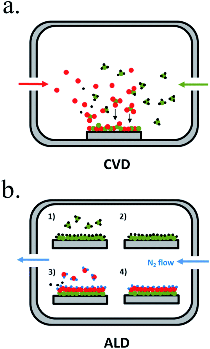 | ||
| Fig. 11 Representative schemes of thin film deposition techniques by (a) chemical vapour deposition (CVD) and (b) atomic layer deposition (ALD). | ||
Atomic layer deposition (ALD) is a variation of CVD in which precursors are introduced in the chamber sequentially, first reported in the 60′ by researchers in the Soviet Union under the name “molecular layering”.186 One of the precursors is introduced to the chamber in an inert gas flow, saturating substrate's surface with the precursor, and then all the non-chemisorbed precursor is removed by the gas flow (Fig. 11b). A second gas is then introduced (normally H2O, O3 or NH3), reacting and forming a conformal submonolayer of the final desired product. This way, control of the layer growth in the sub-nanometer scale is attained, where final thickness depends on the number of cycles of this process.187 ALD is maybe the best candidate to ensure complete surface coverage thanks to saturated deposition steps and thus, to obtain a pinhole-free protective layer.188 ALD also presents lower temperature crystallization due to absorbed molecule mobility but is much more time consuming than CVD.81,189 It has been used for many photoabsorbers and protective materials, even in industrial scale as essential part of high-k gate dielectrics manufacturing, although much more work is needed.189 For covering 3D nanostructures, ALD is the best candidate, due to the self-limited conformal deposition, and has been used in high ratio structures.81
5.2. Strategies and materials for protective films
There are many paths to protect semiconductors from corrosion. In Fig. 12 it was summarized the protective strategies, classified according to an increase in device complexity. From stable semiconductors forming SCLJ with the electrolyte (a), the introduction of metallic layers (thin enough to be transparent) as catalysts and/or to form Schottky junctions (b). Few nanometers thick oxide layers, thin enough to be tunneled, were introduced to increase stability in harsh environments (c). For further stability, thicker transparent films (usually oxides) several tens of nanometers thick can be used, also capable to form an heterojunction with the photoabsorber (d). To maximize charge separation and thus, photoelectrode efficiency, buried junctions can be used, where the protective layer will mainly act as a conductor (e). Finally, the next logical step is use a cable as conductor, forming a non-monolithic device where the photovoltaic part can be located outside of the electrolyte and connected to the electrocatalyzer in a PV-EC configuration (f). | ||
| Fig. 12 Schemes summarizing significant steps in photoelectrode device complexity regarding protective strategies. | ||
Kenney et al.197 fabricated a Ni-protected a silicon photoanode and found that non electrolyte-permeable thick enough metallic layers were also too thick to allow light to reach the photoabsorber. Electrolyte intermixing in the metallic layer (partially oxidized, Ni/NiO) also helped to increase the built-in potential for 2 nm Ni layers, compared with the ≥5 nm Ni/n-Si Schottky junction (Fig. 13a and b). To achieve a good (>80 h) stability, a K-borate + Li-borate solution (pH 9.5) was used. Metallic film permeability in the few nanometers scale was used by Laskowski et al.198 to form an n-Si/5 nm-Ni/10 nm-Au dual working electrode to simultaneously track Ni redox potentials. In another work, Sartori et al. enhanced a p-Si photocathode's built in potential, and thus onset potential, with a simple 5 nm-Ti protective layer together with Pt catalyst particles.199 Obtained photocurrent reached over 25 mA cm−2, but stability was poor. Feng et al. used similar structure but with Ni as catalyst, obtaining more overpotential for the HER reaction.200
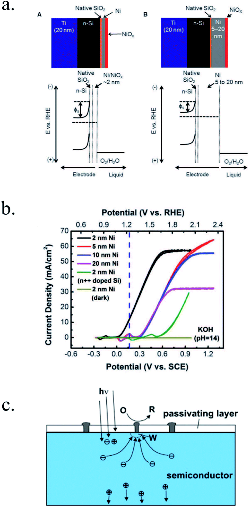 | ||
| Fig. 13 (a) Scheme of n-Si photoanodes protected and catalysed by few nanometer-thick Ni films, demonstrating the effect of extremely thin layers compared to thicker ones. (b) Cyclic voltammogram response of the same Ni-protected silicon photoanodes with different Ni thicknesses, presenting higher photopotential for ∼2 nm films and light absorption if thicker than 10 nm. Reprinted with permission from (Science, 15 Nov 2013, vol. 342, issue 6160, pp. 836–840). Copyright (2013).197 (c) Scheme showing photogenerated charges being collected by the depletion formed between a semiconductor and metallic isles embedded in an insulator transparent protective layer. Reprinted with permission from (Electrochim. Acta 2011, 56, 10726–10736). Copyright (2011) Elsevier.146 | ||
Although interesting results have been obtained with a metallic protective layer, the full potential of the photoabsorbers in long-term stabilities cannot be exploited due to insufficient stability, significant light absorption in the metallic layer and significant recombination in the Schottky junction due to extra states in the interface and Fermi level pinning, lowering photovoltage.201
To overcome metallic film transparency limitations, some works have proposed microstructured surfaces, with Pt islands (∼30 nm thick) in contact with p-Si, and SiO2 covering the rest of the surface, in a balance between surface coverage of catalytic metal and oxide-protected light absorption regions146 (Fig. 13c).
Regarding the limitations of metal-photoabsorber Schottky junctions, Seger et al.202 proposed a buried silicon p–n homojunction in 2012 to maximize electron–hole separation, with a thin Ti metallic film which partially oxidized to TiO2 in the acidic electrolyte and using MoS2 as catalyst. This way, up to 16 mA cm−2 were obtained at 0.2 V vs. RHE (with 0.6 V photovoltage) and 1 h stability. Similar buried junction structure was used by Mei et al.203 using 2–6 nm Ir/IrOx as protective layer in acidic electrolyte, avoiding detrimental SiOx formation.
Silicon dioxide (SiO2) was first studied due to its natural occurrence when Si is exposed to acidic electrolytes on a n-Si/SiO2/Pt photoanode, with poor results.207 Esposito et al.208 fabricated a 2 nm thick SiO2 protected MIS photocathode by controlling the oxidation with rapid thermal oxidation (RTO) and depositing 30/20 nm Ti/Pt islands. Pt was used as HER catalyst, but Ti, with lower work function, enhanced photovoltage and also served as adhesion layer. Although 20/30 nm metallic islands are not transparent, controlling the pitch distance and diameter they could maximize light absorption and catalysis up to photocurrents of 20 mA cm−2 at 0 V vs. RHE and 0.55 V vs. RHE onset potential in 0.5 M H2SO4, with reported 2 h stability.
n-Type silicon photoanodes were fabricated with SiO2 and Ir as catalyst with photovoltages exceeding 500 mV and saturation photocurrents about 30 mA cm−2, although an ultrathin TiO2 protective layer was needed to stop rapid further Si oxidation at oxidative potentials and stabilize for over 8 h the photoanodes in acidic, neutral or basic media206,209 (Fig. 14a and b). Planar and nanopilar p-InP was 3 nm n-TiO2-protected and 2 nm Ru film was added as catalyst, achieving 0.76 V vs. RHE onset potentials and significant photocurrents of 37 mA cm−2 stable for some hours.210 Photoanodes without the TiO2 degraded rapidly during the first hour. In this scheme, increasing TiO2 layer thickness turned into lower trap-mediated thickness-dependent conductivity indicating the importance of using a thin TiO2 layer for efficient tunnelling-mediated electron transport.206,211–213 490 mV photovoltage was also obtained substituting ultrathin TiO2 by Al2O3, finding that tunnelling layers of a thickness >2 nm introduce an intermediate resistance, lower than insulator SiO2 but higher than defect-conductive TiO2.214,215 Crystalline TiO2 was found to reduce insulator-thickness-dependent photovoltage loss in metal–insulator–semiconductor (MIS) type photoanodes, in comparison with amorphous TiO2 (ALD-fabricated at 170 °C), due to dielectric constant increase, with a record photovoltage of 623 mV.216 TiO2 was proven as one of the best candidates, highly protective, and has been identified to be conductive for thicker than 10 nm layers, where tunnelling is highly non-probable. Indeed, hopping via trap states situated ∼1 eV below the conduction band was considered the conduction mechanism in photoanode's case,217 following the concept of “defect band” conductivity, first proposed by Campet et al.218 This will be further discussed in the next section together with other thicker conductive oxides protective layers.
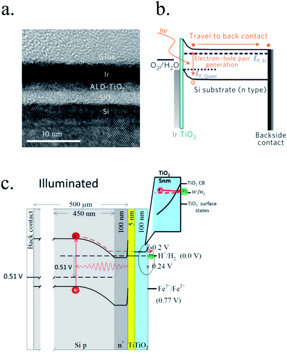 | ||
| Fig. 14 (a) TEM image of an ultrathin ALD–TiO2 + SiO2 protective layer for a silicon photoanode. (b) Equivalent energy band diagram under illumination. Reprinted with permission from (Nat. Mater., 2011, 10(7), 539–44). Copyright (2011) Springer Nature.206 (c) Energy band diagram of a 5 nm Ti/100 nm-TiO2 protected silicon photocathode having a buried p–n junction under illumination. Reprinted with permission from (J. Am. Chem. Soc., 2013, 135, 1057–1064). Copyright (2013) American Chemical Society.227 | ||
Ultrathin oxides, like metallic thin films, are difficult to fabricate being impermeable and pinhole-free for devices lasting hundreds of hours, and majority of the presented works lack long-term stabilities and device fail mechanisms over large device's area.
For an efficient conductivity through protection layers, minimal losses in bulk resistance and semiconductor–electrolyte interface must be attained. The protective layers do not need to be as conductive as conventional transparent conductive oxides as only vertical (some tens of nanometers) conductivity is needed, not in-plane several hundred microns as in solar cells. In general, n-type metal oxide semiconductors have been used to protect photocathodes, based on electrons migrating from the photoabsorber, through the protective layer, and injected in the HER. Fermi level close to the conduction band should help both to form a p–n heterojunction and for favourable alignment with the n-type part of the p–n buried junction. Likewise, p-type semiconductors have been proposed for photoanodes and have efficient OER catalytic surfaces.118,173,219,220 The role of cocatalysts on top of the protective layer and the electrolyte is majorly governed by the pinch-off effect, where with few nanometers thick layers, cocatalysts do not really form a Schottky barrier, and rather what is called “adaptive junctions”.221 Although, material specificities and the formation of recombining contacts have made materials such as TiO2 highly versatile, multiple strategies are possible controlling deposition conditions, oxygen stoichiometry and other metals incorporation for better conductivity or catalysis.213 Transparent and conductive oxides used in the microelectronics industry, such as ITO and AZO, were expected to have good band offsets and conductivity, but their stability and performance resulted very poor.218,222 With thick oxides protective layers such as TiO2, NiO, CoOx and MnO, among others, better results have been achieved in terms of productivity and stability, with tens of mA cm−2 achieved, minimal resistances introduced and several hundred hours, even thousands, of operation tests.
(a) TiO2. Titanium dioxide has been one of the most studied materials as protective layer for small band gap photoelectrodes thanks to its transmittance, relatively good electrical properties and chemical stability. It is an earth abundant metal oxide found in nature and with several fabrication routes, such as anodization, hydrothermal, sol–gel and, for protective layers, mostly known to be fabricated by sputtering and ALD, giving compact layers in comparison with other solution-deposited ones.169 TiO2 is a n-type semiconductor with ∼3.2 eV band gap,6,178 permitting almost complete optical transmittance for visible light spectra, although thanks to its good chemical stability some works have used it also for back-illuminated photoelectrodes.223 Its n-type semiconductor behaviour is known to be caused by oxygen vacancies and thus, Ti3+ states with energy levels close to the conduction band, giving free electrons. TiO2 is known to have significant oxygen mobility under polarization or under different atmospheres annealing, locally forming conductive filaments acting as degenerate n-type material across the whole layer,224–226 explaining various mechanisms reported depending on fabrication and working conditions.186
Photocathodes protection with thick (∼100 nm) sputtered TiO2 was first reported in 2013 by Seger et al.227 in a pn+-Si/(5 nm)Ti/(100 nm)TiO2/Pt structure, where favourable band alignment between n+-Si, Ti/TiO2 and TiO2/Pt interface (behaving like an ohmic contact due to high dopant density of TiO2 and high energy sputtered Pt, rather than like a Schottky junction228,229) introduced negligible resistance or overpotential (Fig. 14c). These findings show the system acting equivalently to a solar cell in series with the catalyst metal. They demonstrated conductivity through the conduction band, also explained to be electron polaron hopping through the Ti3+ states close to the conduction band (∼0.3 eV),230 although the transition temperature between both mechanisms is reported to be about 300 K (room temperature)231 and probably both mechanisms are simultaneously active. Seger et al. introduced a 5 nm Ti layer previous to TiO2 reactive-sputtering deposition to prevent Si substrate from oxidation, a strategy followed by other works145,178,223,232 based on oxygen migration to lowest Gibbs oxide formation energy and thus, oxygen scavenging from Si to Ti.233,234 Up to 20 mA cm−2 at 0.3 V vs. RHE and 70 h of stability were obtained under illumination, corroborating the photoabsorber–protective layer strategy. In following works, durability was studied, reporting the need of 400 °C post-annealing to ALD–TiO2 protective layers synthetized at 200 °C to reach from 8 to 480 h of stability at 0.3 V vs. RHE in 1 M HClO4.235 An increase of doping level under the 400 °C annealing was considered to be the reason of significantly higher conductivity, reducing depletion barrier between the TiO2 and electrolyte, allowing electrons to tunnel through,236 similar results to Liang et al.237 increasing donor level by hydrogen doping upon deposition.
In recent studies from our group, the ALD layer fabrication key parameters for optimal conductivity through 100 nm TiO2 layers were found to be highly related to conductivity through crystalline regions of the film for protective layers both on photocathodes238 and photoanodes.239 Also, amorphous regions were found to be unstable and dissolve in cathodic acidic HER conditions (Fig. 15a and b). The lower crystallization temperature of ALD (∼165 °C) in front of others such as sputtering (requiring deposition or post-treatments at 400 °C)235 makes it an ideal technique to avoid degradation of photoabsorber semiconductors sensible to thermal treatments.240,241 The low deposition temperature was possible thanks to the wide temperature window for TiCl4 precursor.242 Deposition techniques such as high power impulse magnetron sputtering (HPIMS)145 have been used to increase layer's density and thus, minimizing pinholes to avoid electrolyte penetration and anisotropic etch corrosion by KOH (Fig. 15c and d). TiO2 conduction band is close to the HER potential, and with sufficient dopant levels (i.e. oxygen vacancies), electrons can overcome by tunnelling the small potential barrier formed and reach the catalyst.227 Platinum, an expensive noble metal, has been widely used due to its superior cost-efficiency trade-off, and some works have demonstrated the scalability of very small amounts of platinum nanoparticles to drive the PEC water splitting industry to the terawatt level.243
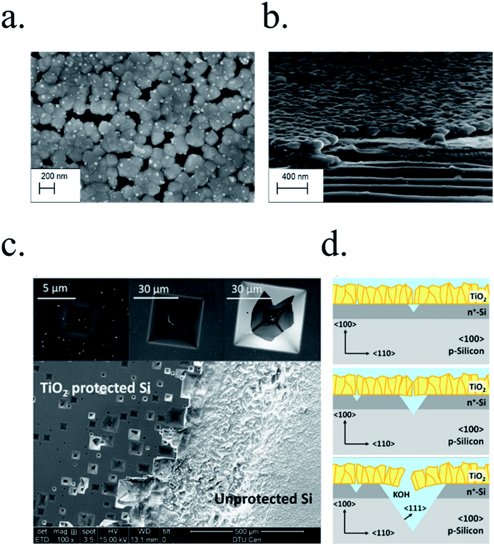 | ||
| Fig. 15 (a) Top and (b) cross section SEM images of an almost-crystalline TiO2 layer after a stability test in 0.5 M H2SO4, wherein dissolution of the amorphous region between crystals can be seen. Reprinted with permission from (ACS Appl. Mater. Interfaces, 2017, 9, 17932–17941). Copyright (2017) American Chemical Society.238 (c) SEM images of a 〈100〉 Si TiO2-protected and unprotected after immersion in 1 M KOH for 3 days. (d) Schematics of the anisotropic etching process forming characteristic inversed pyramids. Reprinted with permission from (Sol. Energy Mater. Sol. Cells, 2016, 144, 758–765). Copyright (2016) Elsevier.145 | ||
Regarding photoanodes, although TiO2 should not be expected to be a good hole-conduction layer, in 2014, Hu et al.217 discovered that depositing amorphous TiO2 on Si, GaAs, and GaP conduction was possible for films up to 143 nm thick (grown by ALD at 150 °C and Ni coated). Energy states about 1 eV inside the forbidden band were observed by high resolution XPS (Fig. 16a). Conductivity through intra-band gap levels was also explained by K. Sivula as “Leaky titania” (Fig. 16b),244 based on the concept theorized by Campet et al. time ago,218 and following works performed thoughtful energy band calculations to explain it.179,245 Deeper studies are necessary, as weak traces of anatase have been reported down to 140 °C.242 McDowell et al.179 found TiO2 films conduction behaviour not unique to amorphous phase (Fig. 16c) and with no relation to carbon or nitrogen impurities, although high temperature treatments turn the system insulator by forming a more-stoichiometric material, reducing available electronic states. Several works have studied thermal treatments under different partial pressures of oxygen and forming gas to understand how conductivity is affected by it.179,186 Nb doping could be a strategy to increment TiO2 conductivity,246,247 but very good conductivity has already been demonstrated if properly fabricated. Other photoabsorbers such as CdTe have been protected with “leaky” amorphous TiO2, with 21 mA cm−2 and 435 mV photovoltage.248 Nickel overlayer was found to be mandatory for proper contact with the conductive TiO2,217 pinning TiO2 energies to Ni states and removing the rectifying space-charge region from the TiO2/solution interface;166,249 this is known for Ni as “adaptive” catalyst.221 Up to 100 h stability and 40 mA cm−2 at 2 V vs. RHE were obtained in 1 M KOH, with 100 nm Ni islands as catalyst.217
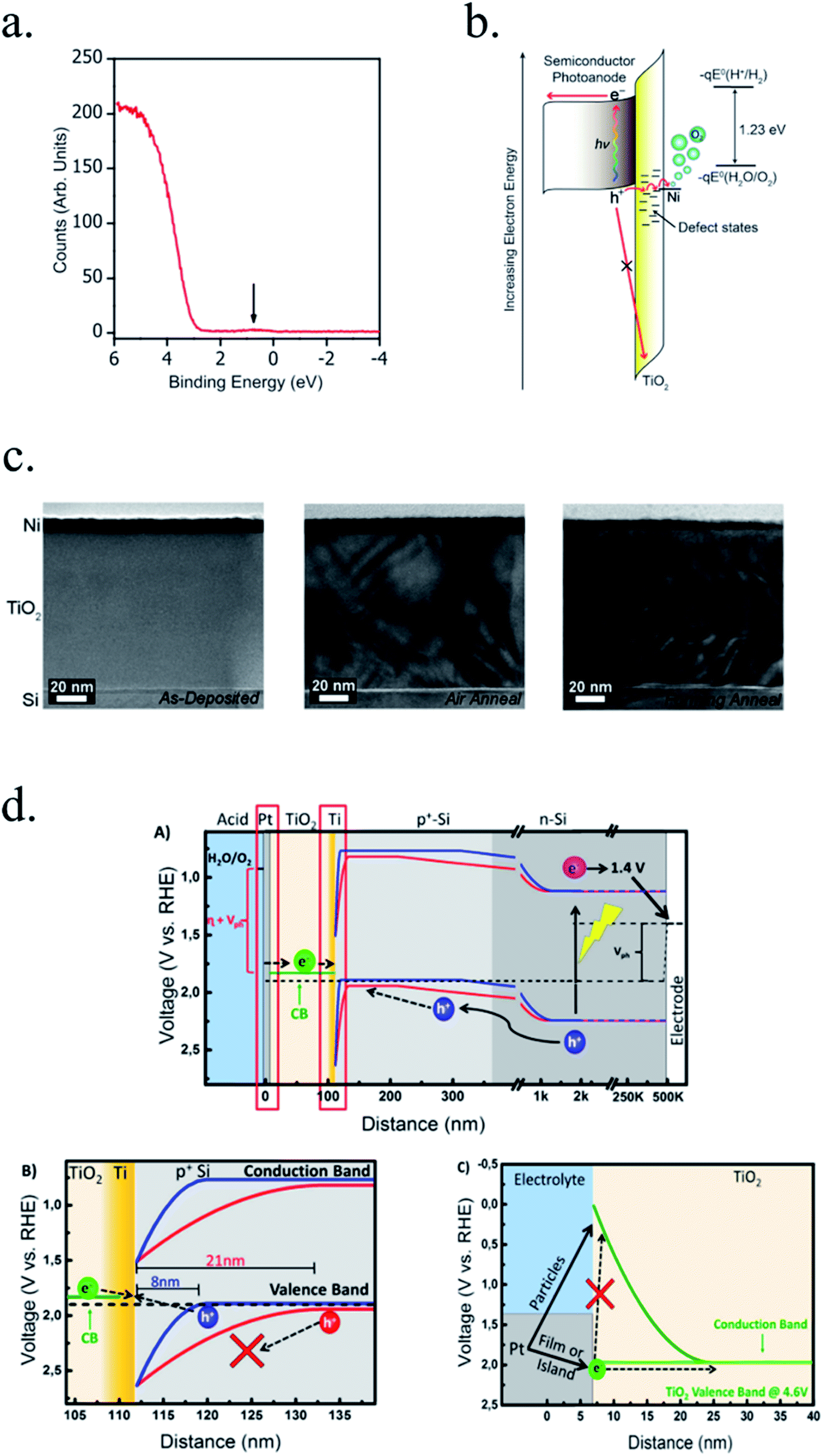 | ||
| Fig. 16 (a) XPS spectrum of 44 nm-TiO2 presenting states inside the band gap. Reprinted with permission from (Science, 30 May 2014, 344(6187), 1005–1009). Copyright (2014) The American Association for the Advancement of Science.217 (b) Schematic energy band diagram to explain the “Leaky” conductivity through intra-band gap states for TiO2-protected photoanodes. Reprinted with permission from (ChemCatChem, 2014, 6, 2796–2797). Copyright (2014) John Wiley and Sons.244 (c) Alternative energy band diagram proposed by Mei et al. where electrons are injected into the conduction band and recombine with p+-Si in an ohmic contact. Reprinted with permission from (J. Phys. Chem. C, 2015, 119, 15019–15027). Copyright (2015) American Chemical Society.252 (d) HRTEM images of as-deposited TiO2 100 nm layers, and air annealed and forming annealed samples presenting crystallinity. Reprinted with permission from (ACS Appl. Mater. Interfaces, 2015, 7, 15189–15199). Copyright (2015) American Chemical Society.179 | ||
Although, in 2015, B. Mei et al.178 designed TiO2-protected (by sputtering at 400 °C) photoanodes and photocathodes where conduction band electron transport was proposed instead of intra-bandgap hole conduction. In the highly doped p+/TiO2 interface, holes from the photoabsorber are considered to recombine with electrons from the conduction band of crystalline TiO2. Electrons are injected in the TiO2 conduction band from the metallic Pt catalyst avoiding TiO2/electrolyte rectifying junction236 and would allow efficient OER (Fig. 16d) stable for over 60 h when using 8 μm Pt islands. In a solid-state measurement for PV applications, Man et al.250 studied n-Si and p-Si devices with amorphous TiO2 deposited by CVD at 100 °C, and found a clear hole blocking behaviour, what would support conduction-band conductivity. Since then, ALD–TiO2-protected silicon nanowire photoanodes stability has been pushed up to >2000 h with 40 nm NiCrOx catalyst film in 1 M KOH.251
In a recent work published by our group,239 completely amorphous TiO2 layers deposited by ALD (100 °C) are found to completely block charge transfer, meanwhile at 150 and 300 °C preferential conductivity paths are observed correlated to defective regions in crystalline TiO2, supporting the conduction band-supported conductivity. These more conductive regions can be correlated to degenerately doped conductive filaments formation, a property known for TiO2.224–226 Confusion with the so-called “leaky amorphous TiO2” might come from local crystallinity at the nanoscale, as it is deposited at temperatures (150–250 °C and sometimes post-treated at 300 or higher179) which are above crystallization. We proved XRD detection is not capable to observe single crystals but they are crucial to conductivity even down to 150 °C, as detected by micro-Raman and i-AFM.
Not so good conductivity stability was found when permeable 5 nm NiFe catalyst was used, and the logarithmic decay over 450 h was attributed to a self-limited passivation of preferential conductivity paths.239 Carefully reviewing the literature, TiO2 conductivity stability in alkaline electrolytes is not so clear to be intrinsic to TiO2 or due to using non-permeable catalysts and high polarizations hindering diminishments (up to 2.07 V vs. RHE248).
(b) NiO. Several works have also studied nickel oxide (NiO) protective layers for water splitting photoelectrodes due to its abundance and chemical resistance, stability, transparency and catalytic properties. With a 3.8–4 eV bandgap253,254 it is not expected to absorb any visible light. Although, significant defects on NiO structure (Ni reduced atoms) can reduce transparency,245,255–257 even presenting electrochromism in specific cases caused by Ni3+ species such as NiOOH.166,256 It has been mainly used for photoanodes protection due to its p-type semiconductor behaviour258 prone to hole conductivity (and electron-blocking properties259) with relatively low resistivity.257,260 NiO has high valence band position as it is based on a d-orbital rather than typical O 2p,261 being slightly reductive to O2 evolution potential, where an accumulation layer will be formed introducing no band bending overpotential.155 Although few works have used it for photocathodes, i.e. a Cu2O electrode 10 nm-NiO protected262 with 70% retained current after 20 min in neutral pH, NiO is reduced in acidic electrolytes155 and cathodic HER potentials.263
Its p-type semiconductivity is given by point defects and Ni2+ vacancies, and is explained by the Mott–Hubbard insulator theory.155 The Ni2+ vacancies contribute with extra oxygen in the structure, which is compensated by oxidation of nickel sites to Ni3+ states, electron acceptors.264–267 Changes in these favorable imperfections due to atomic reorganization caused by temperature treatments, oxygen partial pressure or different layer growth process are crucial in achieving a conductive layer (Fig. 17a).155,254,257,264,268,269 NiO films are known to present oxygen anions migration under polarization,270 up to filament formation,271 which must be taken in account as stoichiometry modifications can reduce or enhance conductivity.
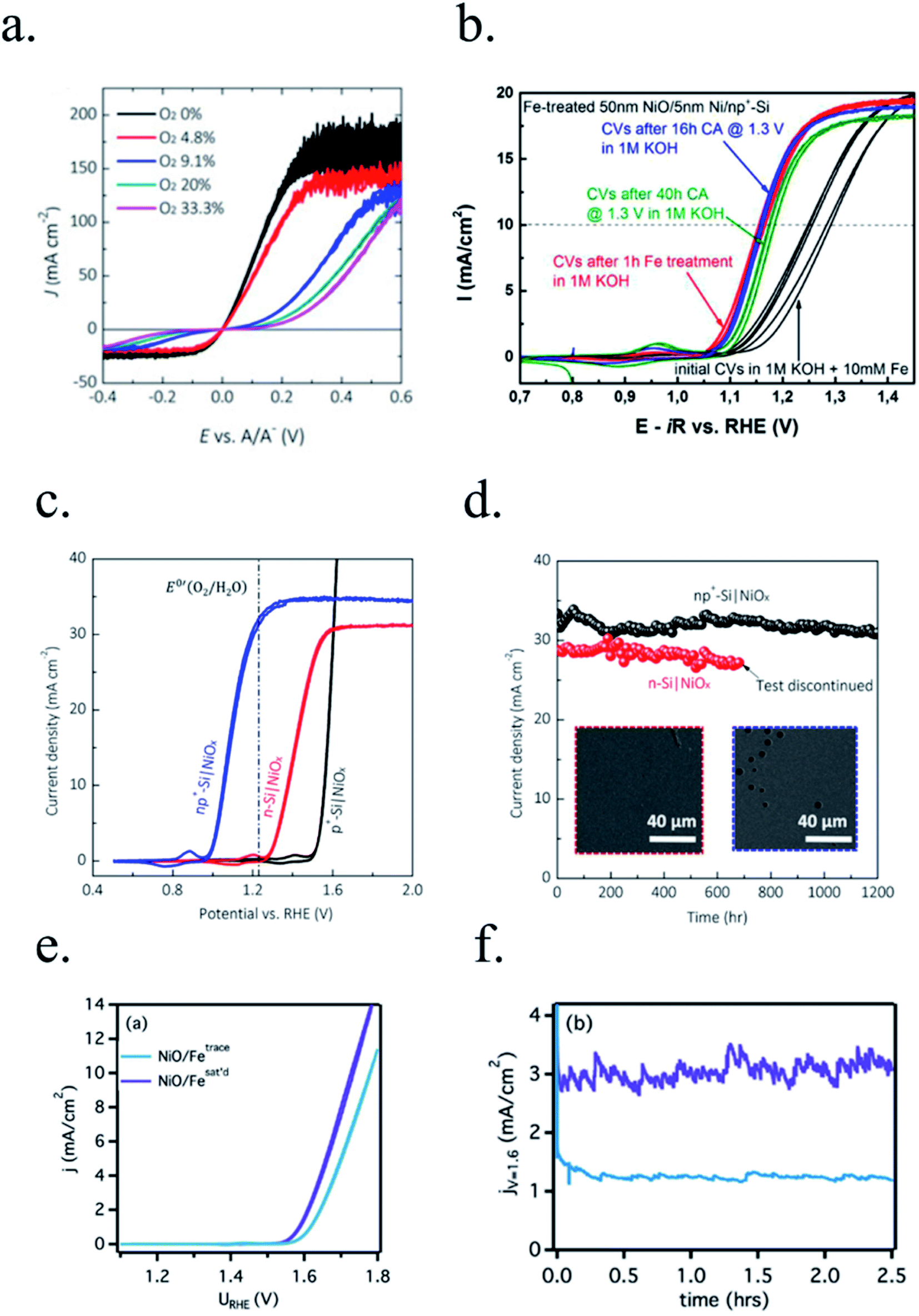 | ||
| Fig. 17 (a) Cyclic voltammograms of NiO layers in 0.35 M Fe(CN)63−/0.050 M Fe(CN)64− in 1.0 M KCl as supporting electrolyte, demonstrating higher oxygen partial pressure during deposition reduces conductivity. Reprinted with permission from (Proc. Natl. Acad. Sci. U. S. A., Mar 2015, 112(12), 3612–3617). Copyright (2015) NAS.254 (b) Cyclic voltammograms of Fe-treated NiO thin films on p+n-Si photoanodes presenting initial activation. Reprinted with permission from (J. Phys. Chem. Lett., 2014, 5, 3456–3461). Copyright (2014) American Chemical Society.284 (c) Cyclic voltammograms and (d) stability at 1.73 V vs. RHE measurement of NiO layers protecting n-Si and np+-Si photoanodes, where higher photopotential can be observed with a buried junction and up to 1200 h stability. Measurements in 1 M KOH and 1 sun illumination. Reprinted with permission from (J. Phys. Chem. Lett., 2015, 6, 592–598). Copyright (2015) American Chemical Society.172 (e) Cyclic voltammograms and (f) stability measurements of anodes ALD NiO coated with traces (blue) and saturated (purple) Fe present in the 0.1 M KOH electrolyte, where higher activity and stability is obtained with more Fe present. Reprinted with permission from (Adv. Energy Mater., 2015, 5, 1500412). Copyright (2015) John Wiley and Sons.279 | ||
Nickel is known to be one of the best earth-abundant OER catalysts in alkaline media,272 where it is highly stable. First trials on nickel-based protective layers were performed directly depositing metallic Ni on top of the photoelectrode and letting it oxidize in contact with the electrolyte, but the hydroxide formed is highly porous and permeable273–275 after oxy-hydroxide species restructuration (migration) during initial operation,272 hydrating up to 10 nm deep. Thicker Ni films, to protect the semiconductor beneath, would still contain a metallic layer, partially absorbing light and reducing photocurrent.197
Nickel-based electrocatalysts are known to be enhanced after cycling at positive potentials,172 related to NiO hydration to NiOOH254 and incorporation of other metal traces, like Fe272,276–278 (with higher activated-state stability with higher amount of Fe incorporated279 and optimized OER catalysis with a 3:1 Ni:Fe ratio280), Co,272 Ru141 or more complex like NiFeP.281 The surface of nickel oxide is affected in its surface by alkaline electrolytes, forming oxy-hydroxides and porous nanoflakes with high surface area272,275 although it is stabilized by the presence of Co, partially inhibiting oxyhydroxide formation and restructuration.272 These hydroxides (Ni(OH)2) and oxy-hydroxides (NiOOH), important in various fields of chemistry and physics,273 are not expected to create significant potential barriers with NiO beneath due to the porous and adaptive junction thanks to abundant electronic states and electrolyte penetration on first nanometers.221,282 Also, it is known to be the responsible of the efficient OER catalysis.
First NiO protected silicon p–n junction was performed in 1987 presenting several high overpotential.283 In 2014, Mei et al.284 used reactive sputtering to deposit 50 nm thick NiO layers on a buried np+-Si homojunction previously protected with 5 nm Ni. It is reported inactive to OER if no pre-treatment in Fe-containing electrolyte was performed (Fig. 17b). This achieved over 300 h stability of silicon photoanodes in 1 M KOH with 14 mA cm−2 at 1.3 V vs. RHE. Soon after, Sun et al.172 reported 75 nm thick RF-sputtered NiO-protected photoanodes giving 30 mA cm−2 at 1.73 V vs. RHE over 1200 h (Fig. 17c and d), where some defects attributed to arc-discharges during RF-sputtering were observed and partial oxygen pressure during synthesis is highly important in resulting conductivity.254 III–V semiconductors such as InP could also be protected with the same kind of layers for over 48 h (ref. 256) or CdTe, HTJ-Si or a-Si:H over 100 h.254 Significant advance was obtained compared with previous attempts from 2012 with sol–gel NiO reaching ∼1 mA cm−2 and losing 50% of performance in 1 h (ref. 285) or 2013 NiRuOx sputtered to form an heterojunction with n-Si giving over 1 h stability with not much photovoltage.141 ALD has only been used for NiO electroactive films few times,279 with Ni(Cp)2 and O3 as precursors at 275 °C deposition temperature. 3–18 nm thick films were found more resistive when ALD deposited than by other techniques together with the need of Fe atoms incorporation for sustained OER current (Fig. 17e and f).
NiO silicon photoanodes protected with 50 nm thick films grown by ALD at temperatures of 100–300 °C, and found to be highly stable over 1000 h but only if periodically depolarized.286 This reversible degradation mechanism was attributed to higher oxidation states like NiO2 being formed, being less catalytic and less conductive, but it must be further analysed. Significant resistance increase at higher than 100 °C deposition temperatures was found, together with less defective films, pointing at a reduction of the p-type behaviour and making the films more insulator. Similar to the 5 nm Ti film pre-deposited for TiO2-protective layers,227 a metallic Ni film could help in avoiding insulator SiO2 detrimental layer formation.
(c) CoOx. Cobalt oxide (CoOx) is a metal oxide similar to NiO in many aspects. With p-type semiconductor behaviour and high conduction band edge, it is favourable to hole conductivity and as electron blocking layer.155 It is expected to be transparent to large part of visible spectra due to its ∼2.3 eV band gap.287,288 It is hydroxylated in contact with alkaline media into CoOOH, a known stable and active catalyst for O2 evolution (OER),289 forming nanosheet/nanoflake structures290,291 (Fig. 18a). Its OER catalysis is highly enhanced by fabricating it already containing Fe291,292 or incorporating Fe from the electrolyte291 with low overpotentials (∼250 mV @ 10 mA cm−2), close to NiFe.290 Depositing few nanometers ALD CoOx on np+-Si photoanodes up to 30 mA cm−2 were obtained by Yang et al. 1.4 V vs. RHE in 1 M NaOH and 1 sun illumination stable for 24 h.293
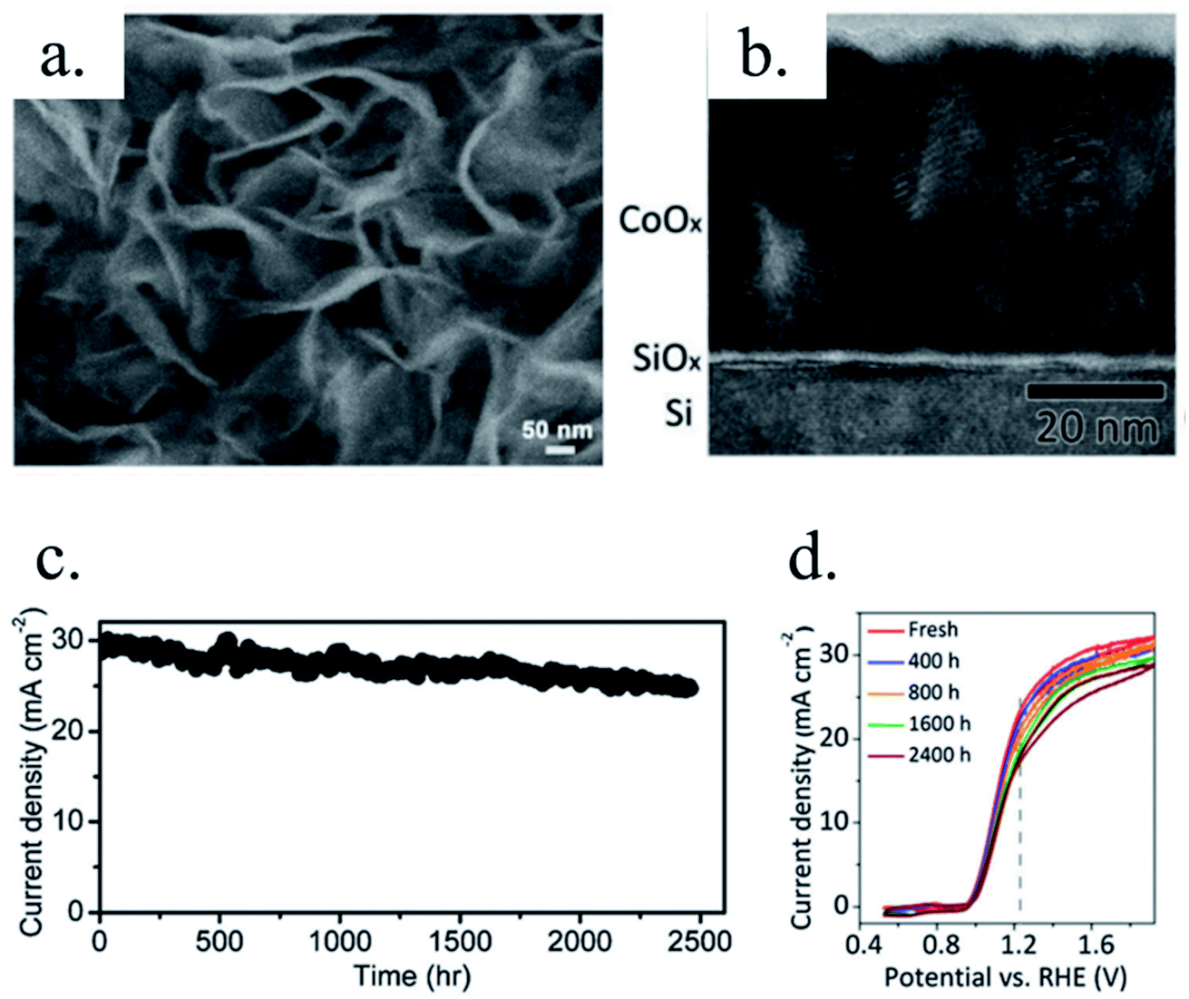 | ||
| Fig. 18 (a) SEM image of Co(OH)2 electrodeposited for 2 min. Reprinted with permission from (Nanoscale, 2016, 8, 9667–9675). Copyright (2015) RSC.290 (b) High resolution cross section TEM images of polycrystalline CoOx-protected n-Si photoelectrode. (c) Stability measurement at 1.63 V vs. RHE and (d) cyclic voltammogram of the CoOx-protected n-Si photoelectrode under 1.1 sun illumination in 1 M KOH. Energy Environ. Sci., 2016, 9892 – published by The Royal Society of Chemistry (RSC) on behalf of the Centre National de la Recherche Scientifique (CNRS) and the RSC.295 | ||
Bae et al.287 sputter-deposited 50 nm thick NiCoOx protective layers on back-illuminated photoanodes, reaching stabilities over 72 h and 22 mA cm−2 at 1.23 V vs. RHE at pH 14 and further enhanced by Fe traces incorporation from the electrolyte. Xing et al.294 co-sputtered CoOx with 3–8% vanadium 70 nm thick layers on 2 nm Cr protected p+n-Si textured photoanodes, with almost 30 mA cm−2 at 1.23 V vs. RHE. Zhou et al.295 CoOx protected by ALD an n-silicon photoanode containing a thin SiO2 layer to form a SIS heterojunction, reaching 570 mV photovoltage and 30 mA cm−2 at 1.23 V vs. RHE and stable for up to 2500 h at 1.63 V vs. RHE in 1 M KOH (Fig. 18b–d). Burke et al.291 cathodically electrodeposited Co1−xFex(OH)2 ∼50 nm thick finding that the incorporation of Fe reduced up to 100 times OER overpotential compared to pure CoOOH thanks to strong Co–Fe coupling up to 60% Fe, but at higher amounts, conductivity was reduced and the layer dissolved as FeOOH is soluble in basic mediums unless incorporated in NiOOH or CoOOH. This would suggest CoOOH acts as “conductive, chemically stable, and intrinsically porous/electrolyte-permeable host for Fe, which substitutes Co atoms and serves as the (most) active site for OER catalysis”. Other metals such as Ru or Rh have been combined with CoOx to further reduce its OER.296 Tung et al.289 found one of the causes of long-term instability is volume expansion on phase change due to hydroxylation to CoOOH, and thus, nanoscale structuration can prevent detachment and efficiency loss.
(d) Other conductive protective layers. Back in 1987, Kainthla et al.297 protected n-Si with MnO achieving stable photoanode for 650 h giving 1 mA cm−2 at 1.6 V vs. RHE in 0.5 M K2SO4 solution. In 2012, up to 20 nm ALD MnO films were used by Strandwitz et al.140 to protect n-Si and obtained almost 30 mA cm−2 at 1.5 V vs. RHE in 1 M KOH and 550 mV photovoltage, but not stable for more than 10 min. They also found film thickness increase introduced significant resistance, affecting fill factor.
Transparent and conductive thallium oxide (Tl2O3) was deposited 3–4 μm thick by Switzer et al.298 protecting an n-Si photoanode. A SIS junction was formed, with over 500 mV photovoltage and 33 mA cm−2 photocurrent with a Fe(CN)63+/4+ redox couple, although thallium is a toxic and expensive material with quite low abundance.299
∼100 nm sputtered n-type Nb2O5 formed an heterojunction with p-type GaP in a work by Malizia et al.,300 achieving 710 mV photovoltage, although its stability was found less than TiO2 protective layers in 1 M HClO4 attributed to Nb2O5 detachment and thus, Pt cocatalyst loss (Fig. 19a). Avoiding pinholes corroding photoabsorber beneath is important, as some materials such as Nb2O5, with expected good stability in acidic environments,301 will not stop corrosion from beneath.
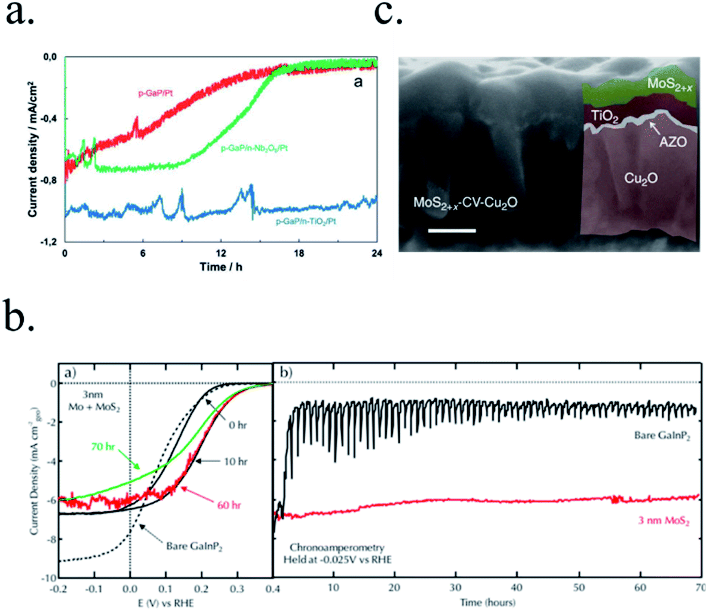 | ||
| Fig. 19 (a) Stability measurements of GaP photocathodes unprotected (red) Nb2O5 (green) and TiO2 protected (blue) in 1 M HClO4. Reprinted with permission from (J. Mater. Chem. A, 2014, 2, 6847–6853). Copyright (2014) RSC.300 (b) Stability measurement of a GaInP photocathode with and without 3 nm MoS2 catalyst and protective layer. Reprinted with permission from (J. Phys. Chem. Lett., 2016, 7, 2044–2049). Copyright (2016) American Chemical Society.303 (c) SEM cross section image of a Cu2O photocathode AZO/TiO2/MoS2+x protected. Reprinted with permission from (Nat. Commun., 2014, 5(1), 1–7). Copyright (2014) Springer Nature.121 | ||
For GaP nanowires, Standing et al.302 directly grew a 20 nm electrochemically produced oxide Ga2O3 slightly increasing photovoltage and enhancing stability before depositing either Pt or MoS2 HER catalysts. The list of possible protective layers will probably increase following years, as other authors have proposed other combinatorial metal oxides such as CuWO4, Co3O4, SnO2, WO3, Ta2O5 for photoanodes or BaTiO3 and Ta2O5 for photocathodes.112
Non-oxide materials have also been studied. Among them, MoS2/MoSx, one of the best performing earth-abundant catalyst for the HER reaction,304 has been used few times not just as catalyst, but also as protective layer. 1–5 nm of MoS2 increases GaInP and Si photoelectrodes stability (Fig. 19b)303 in acidic electrolytes. However, in 2012 Seger et al.202 protected an n+p-Si homojunction with 9 nm Ti and 35 nm MoSx, and they attributed protection to Ti, on a self-limited oxidation to TiO2. Other authors have combined up to 100 nm MoSx with TiO2 to protect Cu2O photocathodes (Fig. 19c).121,305 Laursen et al.306 protected with MoS2 a silicon photocathode by sputtering 10 nm Mo and reactive-annealing it with H2S at 450 °C, obtaining stable photocathode for 120 h in 1 M HClO4. Recently, King et al.307 protected a n+p-Si with 3.7 nm SiO2 and ∼11 nm MoOx/MoS2 (metallic Mo is sputtered and further H2S atmosphere annealed) achieving up to 62 days (1638 h) stability with >10 mA cm−2 photocurrent at 0 V vs. RHE in 0.5 M H2SO4.
6. Heterojunctions with the protective layer
Creating effective short band gap photoelectrodes requires highly conductive, transparent, stable and kinetically efficient protective layers and catalysts, but also to maximize the photovoltage of the system. For sensible-to-corrosion photoabsorbers, the electrolyte will not be in contact with the photoabsorber due to the introduction of the protective layer in between and thus, a semiconductor–liquid junction (SCLJ) will not be present to create an electric field to separate and extract photogenerated charges.Forming an electronic junction between two different materials (at least one of them a semiconductor) forms an heterojunction. In this case, the maximum photovoltage of the photoelectrode is governed by the electronic properties of protective layers, photoabsorbers and interfacial energetics. Introducing heterojunctions results in a more complex device (Fig. 12b–d), meanwhile it opens the possibility for higher photovoltages thanks to a larger amount of candidates available. Among them, three types of heterojunctions are considered: Schottky junctions (formed between a metal and a semiconductor), metal–insulator–semiconductor (MIS) junctions and semiconductor–semiconductor heterojunctions (composed of different materials).
6.1. Schottky and MIS junctions
In Section 5 has been analysed how thin (few nanometers) metallic films can protect a semiconductor from corrosion, forming a Schottky junction (Fig. 12b). However with limited stability and with significant recombination rates and Fermi level pinning caused by states in the metal–semiconductor interface, limiting electron–hole pseudo-Fermi level separation and thus, the photovoltage.201 Even so, selecting appropriate metals with work functions low for photoanodes and high for photocathodes is mandatory to obtain significant photocurrents and photovoltages.190 Very small photovoltages are obtained from just directly depositing Pt or Ni on p-Si, meanwhile 200 mV more can be generated with a p-Si/5 nm Ti contact previous to Pt catalyst (Fig. 20a)196,199 or Ni catalyst200 thanks to higher Schottky barrier created by the favourable work function of Ti. | ||
| Fig. 20 (a) Cyclic voltammogram of p-Si photoanodes where higher photovoltages can be observed if 5 nm Ti is used to form the Schottky junction and Pt on top as HER catalyst. Reprinted with permission from (Electrochim. Acta, 2018, 271, 472–480). Copyright (2018) Elsevier.199 (b) Cyclic voltammograms of n-Si photoanodes presenting higher MIS photovoltage if Al2O3 is used as ultrathin insulator layer and Pt as the metal intervening thanks to its work function, together with Ni as OER electrocatalyst. Reprinted with permission from (Nat. Commun., 2017, vol. 8, 15968). Copyright (2017) Springer.308 (c) Cyclic voltammogram and (d) scheme depicting the formation of adventitious interfacial ultrathin SiO2 preventing Fermi level pinning due to electrolyte (pH 9.8 K-borate buffer) penetration, and thus, forming higher photovoltage. Reprinted with permission from (Energy Environ. Sci., 2017, 10, 570–579). Copyright (2017) RSC.198 | ||
Introducing few nanometers of insulator materials between the semiconductor and the metal film (Fig. 12c), such as SiO2 or Al2O3,201,308 can passivate interfacial electronic states and enhance energy level separation in the heterojunction (forming a metal–insulator–semiconductor junction, MIS). Specifically, Al2O3 is favourable to unpin the Si Fermi level, giving extra built-in potential. Regarding selected metal, Pt has higher work function than Ni and increases photovoltage in n-Si photoanodes (Fig. 20b).308 Laskowski et al.198 suggest high barrier regions are formed when Si is oxidized to SiO2 due to electrolyte (pH 9.8 K-borate buffer) permeability in very thin (∼3–5 nm) Ni films, avoiding Ni/n-Si Fermi level pinning and thus, increasing photovoltage (Fig. 20c and d).
Following this, several works have focused on the passivation of Si surface states with ultrathin semiconductor layers (0–12 nm) such as TiO2, although the junction is formed between the metallic film on top and the silicon, and thicker intermediate layers will increase metal to semiconductor separation, reducing formed photovoltage.212 SrTiO3 epitaxial films, MBE-deposited by Ji et al.309,310 on p-Si with patterned 50 nm Ti/Pt catalyst formed a stable (>35 h in 0.5 M H2SO4) and effective photocathode (35 mA cm−2 at −0.4 V vs. RHE, 450 mV photovoltage) when only few unit cells (4–6, ∼1.6 nm) of the strontium titanate were deposited. The space-charge region is formed between the p-Si and metallic Ti, with lower work function than Pt, as it has a work function similar to p-Si, and would generate small photovoltage. Although, these insulator layers introduce significant tunnelling resistance if thicker than 3 nm (ref. 186) and do not significantly increase stability to corrosion.
6.2. Semiconductor–semiconductor heterojunctions with thick oxides
Similar schemes can be formed with thicker conductive oxides semiconductors instead of metals (Fig. 12d), overcoming metal films limitations on thickness and transparency. In this case, heterojunctions between two semiconductor materials will be formed, where a thin insulator film can be introduced in the interface avoiding Fermi level pinning if necessary (forming a semiconductor–insulator–semiconductor (SIS) junction). Similar electronic structure to Section 3.6 will be formed, but doing so with a short band gap material and a wide band gap metal oxide has a great benefit: the major part of photon absorption will occur in the short band gap one, collecting large portion of the visible spectra. Also, short band gap materials such as Si, GaAs or CIGS are very good photoabsorbers, with minimal recombination and transport losses.Thicker-than-tunnelling metal oxides have been widely used both to protect short band gap semiconductors and to generate a built-in electric field. N-type wide band-gap semiconductors such as ZnO, WO3 or TiO2 have favourable energetics to form a heterojunction with p-type photoabsorbers such as Si, InP or CIGS in a similar strategy to SIS solar cells.311 In 1996, Yoon et al. tested a different thickness n-type WO3 on p-Si, achieving a better photovoltage by controlling resistivity, carrier concentration and surface band bending (Fig. 21a).312 In 1998 (ref. 313) they electron-beam evaporated 50 nm WO3 on top of p-Si with 1–2 nm Pt as catalyst, and the role of a more efficient built-in field is clearly observed when introducing WO3, with a better HER catalysis when Pt is incorporated (Fig. 21b). Although, WO3 was found not to be stable if Pt was not blocking direct contact of WO3 with the acidic electrolyte (0.1 M H2SO4). By the introduction of an indium-doped tin oxide (ITO) layer, Coridan et al.314 demonstrated not such a good interface is formed between WO3 and Si, and the ITO layer could also act as an ohmic contact, allowing them to create a tandem cell. Wang et al.315 also demonstrated Fe2O3 heterojunction with n-Si and p-Si photoelectrodes.
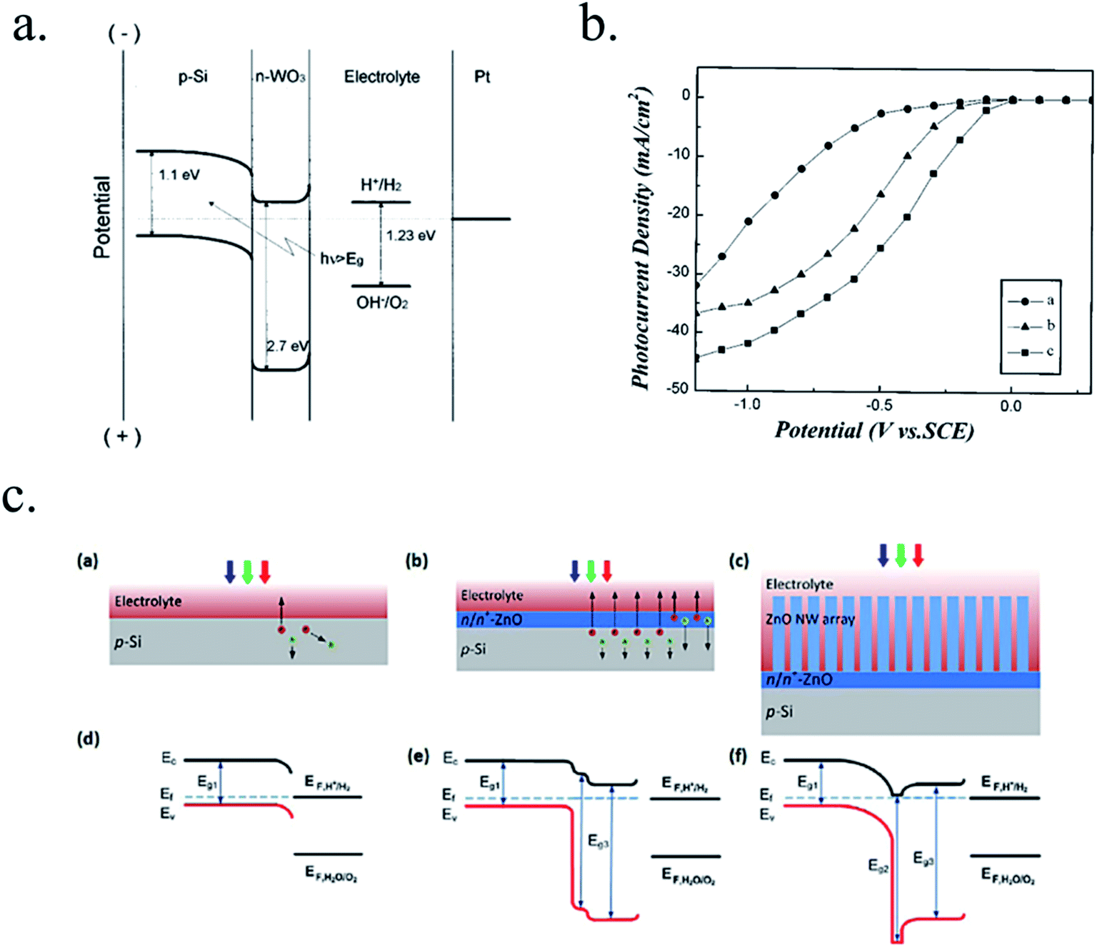 | ||
| Fig. 21 (a) Scheme of a p-Si/n-WO3 heterojunction. Reprinted with permission from (J. Appl. Phys., 15 May 1997, vol. 81, no. 10). Copyright (1997) AIP Publishing.312 (b) Cyclic voltammgrams of a p-Si, a p-Si/n-WO3 and a p-Si/n-WO3/Pt catalysed photoelectrodes. Reprinted with permission from (J. Appl. Phys., 1 October 1998, vol. 84, no. 7). Copyright (1998) AIP Publishing.313 (c) Schemes (top) and energy band diagrams (bottom) of p-Si (left) p-Si/n+-ZnO (center) and p-Si/n+-ZnO/ZnO-NW (right). Reprinted with permission from (Nanotechnology, 2012, 23, 194013). Copyright (2012) IOP Publishingng.316 | ||
Transparent conductive oxides (TCO) such as ITO and AZO were tested, as theoretically should be good conductive and transparent n-type semiconductors for photocathodes and thus, form good p–n heterojunctions. ZnO (∼3.1 eV) was deposited by Sun et al. as a film and as nanorods on planar p-Si and nanowire-grown p-Si,316 achieving better light absorption and active surface area thanks to the nanostructures and HER catalysis enhanced by Ni, Pt and Pd cocatalysts (Fig. 21c). p-Type Cu2O electrodes can also form an heterojunction with n-ZnO reaching more than 7 mA cm−2, although TiO2 was required for higher stability even in 1 M Na2SO4 at reductive potentials.92,121 Although, stability was limited to few minutes as ZnO is an amphoteric metal oxide unstable in alkaline and even more in acidic electrolytes.317
Designing a photocathode with TiO2 as n-type semiconductor and transparent protective oxide forms a p–n junction when put in contact with a p-type photoabsorber such as Si, InP or CIGS. Seger et al.236 deeply studied the built-in fields generated between p-Si and TiO2, and in the TiO2-electrolyte interface (Fig. 22a–c), with depletions only possible to be tunneled through if doping levels are high enough. Lin et al.318 demonstrated the junction formed between p-InP and 10 nm n-TiO2 (Fig. 22d). Azarpira et al.319 deposited ∼100 nm n-type Pt-doped anatase TiO2 on p-type Cu(In,Ga)Se to form the heterojunction of a photocathode, with Pt also enhancing HER catalysis (Fig. 22e and f). 300 mV photovoltage was achieved, with onset potential at ∼0.23 V vs. RHE but photocurrent saturation (37 mA cm−2) at −0.3 V vs. RHE, significantly worse than a commercial CIGSe PV cell. This is because directly depositing one on top of the other does not take into account interfacial recombination, states passivation, etc., which have been circumvented in CIGSe PV devices by highly optimized superficial pre-treatment, n-type CdS chemical bath deposition and multilayer TCO top contact.320 Thus, directly depositing TiO2 in top of a short band gap photoabsorber is a simpler strategy but maybe not so effective as protecting a buried solar cell.240,241,321
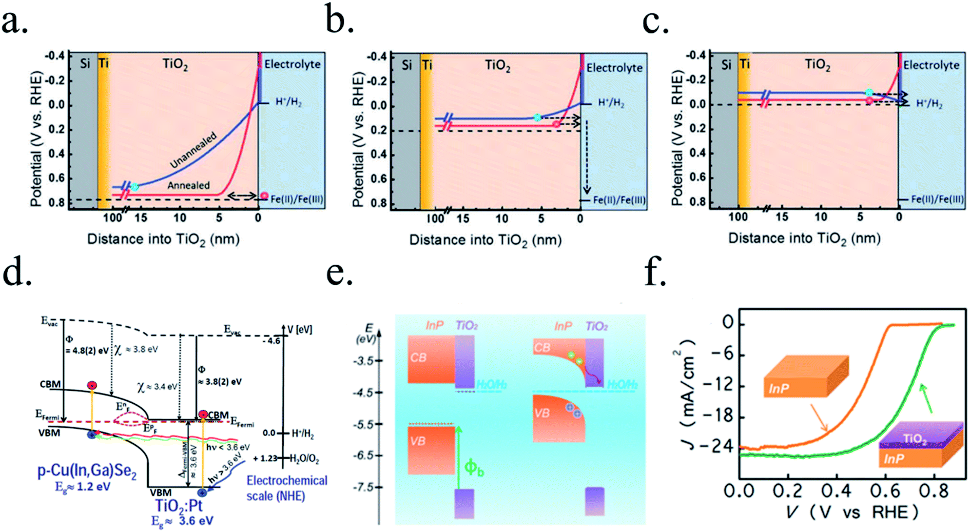 | ||
| Fig. 22 The effect of annealed and unannealed TiO2 protective layers on detrimental superficial band bending at different potentials (a) +0.77 V vs. RHE, (b) +0.2 V vs. RHE and (c) 0.0 V vs. RHE. Reprinted with permission from (J. Mater. Chem. A, 2013, 1, 15089). Copyright (2013) RSC.236 (d) Heterojunction formed between a p-CIGSe and n-TiO2:Pt film. Reprinted with permission from (Adv. Energy Mater., 2015, 5, 1402148). Copyright (2015) John Wiley and Sons.319 (e) Energy band diagrams and (f) cyclic voltammograms response of an InP/TiO2 heterojuncton. Reprinted with permission from (J. Phys. Chem. C, 2015, 119, 2308–2313). Copyright (2015) American Chemical Society.318 | ||
Metal oxide protective layers acting as part of the heterojunctions for photoanodes also introduce some benefits. Transition metal oxides such as CoOx155,293 or NiO285 have high work function due to oxygen vacancies and cation oxidation states,322 what can be used when designing photoelectrodes heterojunction to increase built in electric field and also as hole transporter and electron blocking layers. 37 nm sol–gel nickel oxide can form a 300 mV photovoltage285 and 75 nm sputtered NiO ∼350 mV (ref. 172) on n-Si. Although, these photoanodes are far from the photovoltages obtained with buried p–n junctions (550–600 mV)172 due to Fermi level pinning in the Si-MOx interface. Almost no photovoltage is obtained with a p-NiO/n-InP heterojunction due to strong pinning, whereas with a buried p+n-InP ∼700 mV were obtained.256 Zhou et al.323 coated n-Si photoanodes having ∼2 nm SiOx or ∼2 nm SiOx/2–3 nm ALD–CoOx with ∼100 nm sputtered NiO, and found the thin CoOx interlayer introduces up to 165 mV extra photovoltage reaching 560 mV helped by the de pinning caused by the thin SiO2 (Fig. 23a and b). CoOx increases band bending at the interface due to 120 mV larger work function of CoOx in respect to NiO. This way, photovoltages close to n+p-Si junctions and 30 mA cm−2 stable for 1700 h (70 days) were obtained. Other p-type semiconductors such as Fe2O3 (ref. 12 and 324) have been used to form heterojunctions with n-Si.
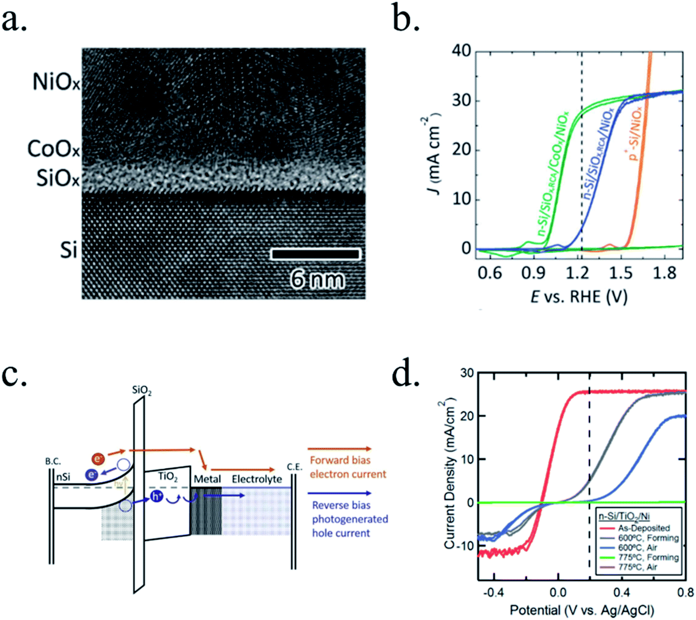 | ||
| Fig. 23 (a) HRTEM cross section and (b) cyclic voltammograms of an n-Si/SiOx/CoOx/NiOx SIS junction (green), where higher photovoltage is obtained thanks to 120 mV greater CoOx work function. Reprinted with permission from (Energy Environ. Sci., 2015, 8, 2644–2649). Copyright (2015) RSC.323 (c) Band diagram of an n-Si/SiO2/TiO2/metal/electrolyte photoanode presenting hole hopping through TiO2 intra-band gap states. Reprinted with permission from (J. Electrochem. Soc., 2016, 163(3) H192–H200). Copyright (2016) IOP Science.325 (d) Cyclic voltammograms of n-Si/TiO2/Ni photoanodes treated at various temperatures, showing SIS junction detrimental effects with high temperature treatments by reducing states availability in TiO2. Reprinted with permission from (ACS Appl. Mater. Interfaces, 2015, 7, 15189–15199). Copyright (2015) American Chemical Society.179 | ||
As explained in Section 5.2.3(a), TiO2, although being an n-type semiconductor, has been reported to be efficiently conductive for water oxidation when grown amorphous, with mid-bandgap states (∼1 eV below the conduction band) allowing hole conductivity by hopping through them217,244,325,326 after tunnelling through the thin SiO2 interface. These energy states are considered to equilibrate with n-Si Fermi level, generating photovoltage (Fig. 23c). Ni catalyst was reported to be mandatory for properly contacting these estates through a less defective TiO2 surface and thus, allowing connexion with the OER catalysis.186,217 The fabrication process (ALD, sputtering) and specific doping conditions of TiO2 (caused by post-annealing process modifying the Ti states density, carbon contaminants, etc.) has been reported to be highly related to final SIS junction photovoltage in a n-Si/TiO2/Ni photoanode (Fig. 23d).179 Heterojunctions with the amorphous TiO2 have also been fabricated with other photoabsorbers, such as n-CdTe/TiO2/Ni, with 435 mV photovoltage and 21 mA cm−2.248 If protective layers do not have the optimal energy band levels and interface energetic states, degenerately doped layers will screen metallic catalyst work function and limit performance.186 Meanwhile, slightly doped protective layers, if thicker, will introduce overpotentials from electrical resistivity, proportional to metal oxide thickness. To prevent this, buried junctions can maximize the obtained photovoltage by themselves, not depending on the protective layer.
7. Buried homojunctions to maximize efficiency and cell flexibility
As it has been analysed in previous section many efforts have been put in forming heterojunctions to directly create a built-in field between the metal oxide protective layer and a short band gap semiconductor. So far, even the achieved photovoltages have been significant, they are not as high as the ones for short band gap semiconductors reported for photovoltaic solar cells (with open circuit potentials of up to 750 mV).133,327 Buried p–n junctions (Fig. 12e) have been proven to generate higher built-in electric fields than SCLJ or Schottky junctions, decoupling photoabsorbers Fermi level from that of the metallic or oxide protective layer or electrolyte, also removing a constrain on the catalyst required work function value.186,328 This way, a more flexible device design is possible as each component (photoabsorber, protective layer and catalyst) can be selected more independently, as it can be observed in Fig. 24a and b. Thus, several groups have shifted the strategy and worked on adapting solar cell p–n junctions for water splitting, obtaining some of the highest reported performances of PEC cells.155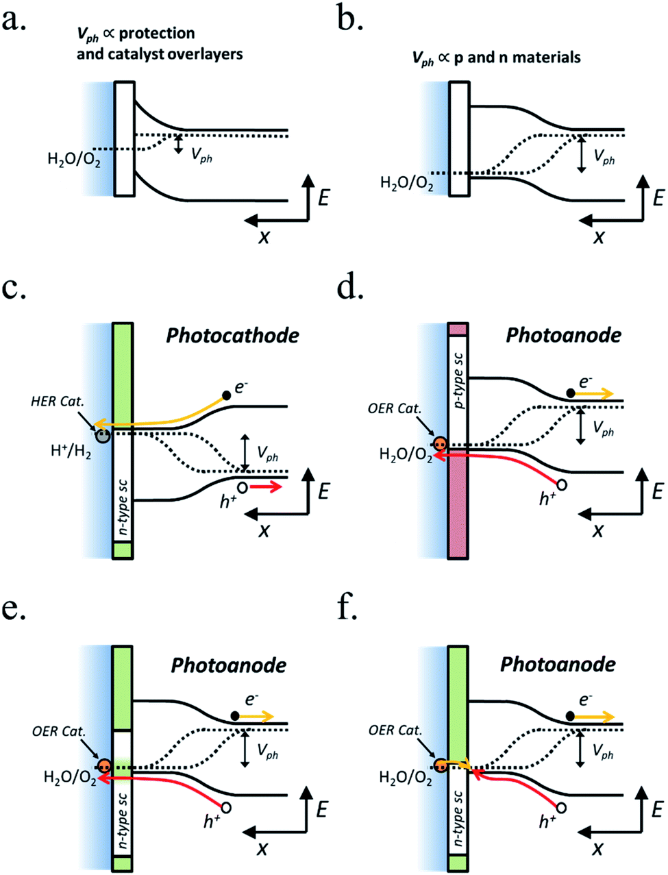 | ||
| Fig. 24 Energy band schemes of (a) a junction depending on the photoabsorber/electrolyte interface or intermediate layers (i.e.: SCLJ, Schottky, MIS, SIS, …) and (b) a buried junction, only dependent on the semiconductor materials forming the junction quality (i.e.: n-Si/p-Si, CIGS/CdS, …). (c) Photocathode protected with an n-type semiconductor layer. (d) Photoanode protected by a p-type semiconductor hole transporting layer. Photoanodes protected with n-type semiconductors layers thanks to (e) mid-band gap states conducting holes and (f) contact for electrons recombining with holes from the photoanode. | ||
Several photovoltaic-used schemes have been studied, being silicon the most implemented one by far. Not only because is the most used one for solar cells, dominating the solar panels market, but also because of the simple and robust cell obtained: a monocrystalline silicon solar cell can be fabricated several tens of centimetres wide, few hundred microns thick and is robust, not requiring any substrate. Also, as p–n junctions are fabricated in silicon wafers by dopant diffusion and incorporation in its crystal lattice at fabrication temperatures of up to 1025 °C,178 further thermal steps applied at medium temperatures (up to 500 °C) will not damage the p–n junction and will retain original output. In a buried junction electrode, photogenerated charges will migrate to the catalyst/electrolyte interface through protective layers, acting as conductive contacts: n-type semiconductor protective layers should be expected to be prone for electron conductivity in photocathodes (Fig. 24c), and p-type semiconductors for holes in photoanodes (Fig. 24d). Although, other strategies such as mid-band gap states in n-type semiconductors have been proposed for hole conduction (Fig. 24e) or recombining contacts (Fig. 24f), as has been discussed in Section 5.2.3. As example, photovoltages as high as 630 mV have been obtained for silicon with buried p–n junctions.327 Other semiconductors have been tested apart from silicon with same protective and catalyst strategies, proving these to be highly reproducible in other photoabsorber materials, increasing device flexibility.329
As it was reported by Scheuermann et al.212 and Wang et al.,329 once a buried junction is introduced in our device, the requirements of the protective layer or the co-catalyst metallic film are reduced. Optimal work function metallic films or cocatalysts to create high electric field with the photoabsorber are no longer needed, widening material selection possibilities. The protective layer just needs to be chemically stable, highly conductive, transparent and the surface must not create electronic barriers with the electrolyte, together with being kinetically efficient for the HER or OER reactions, normally achieved by the addition of co-catalyst particles or films. What is equally necessary, though, is that no electrical barriers formed between the top contact of the p–n junction and the protective layer.
Several works have obtained this by creating degenerately doped ohmic contacts, the most used case for silicon being p+/n+ (acting like metals) top contacts in the photoanode/photocathode buried junction, shielding the built-in electric field from protective layer's interaction. Even if an upward band bending is present on the n+/p+ surface, its depth would be limited to few nanometers due to the high doping level, easily permitting charge tunneling through these depletions, facilitating the ohmic contact.203,227,329 Seger et al. introduced a metallic 5 nm Ti film between n+p-Si and MoSx202 or TiO2,145,227 to form an ohmic contact and to prevent Si oxidation into detrimental insulator SiO2 (Fig. 25a), meanwhile in a photoanode, for Mei et al.178 a similar structure acted as an ohmic recombining contact between holes from p+-Si and electrons from TiO2 conduction band (Fig. 25b).
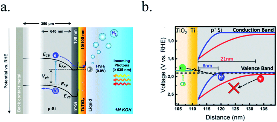 | ||
| Fig. 25 Metallic thin Ti films on degenerately-doped silicon assuring ohmic contacts in (a) a photocathode (reprinted with permission from (Sol. Energy Mater. Sol. Cells, 2016, 144, 758–765). Copyright (2016) Elsevier.145) and (b) a photoanode, where holes recombine with electrons from the conduction band of the protective layer (reprinted with permission from (J. Phys. Chem. C, 2015, 119, 15019–15027). Copyright (2015) American Chemical Society252). | ||
An example of the benefits of a buried p–n junction is the work by Scheuermann et al.,212 where they tried to maximize n-Si photoanodes with few nm SiO2 or SiO2/TiO2 layers and Ir as catalyst, reaching limited 500 mV photovoltage (highly sensible to SiO2 thickness), whereas with a buried n+p-Si junction independent 630 mV were obtained. Similar maximum photovoltages for n-Si/p-Si and n+p-Si/p+n-Si PEC electrodes have been obtained by other authors.140,165,197,202,203,206,212,217,227,235,238,239,286,330
In recent years, several other examples of buried junctions can be found, resembling solar cell structures with other materials. In 2014, Kast et al.232 protected a commercial textured n+p silicon solar cell with 10 nm Ti/50 nm F:SnO2/50 nm TiO2 and 2 nm Ir as HER catalyst to form a photocathode, obtaining onset potentials ∼0.6 V vs. RHE and >30 mA cm−2. 610 mV photovoltages were produced by a CoOx protected p+n-Si photoanode293 or >550 mV with a radial n+p junction on Si nanowires.328
Also, Bae et al. fabricated a silicon photoanode287 and a thinned photocathode (Fig. 26a and b)223 to be back-illuminated, a configuration which would easy creating a tandem between two electrodes for a bias-free reaction. For it, they used similar strategies as previously reported: degenerately doped p+/n+ Si surfaces with 50 nm NiCoOx/5 nm Ti-100 nm TiO2–Pt respectively for efficient OER/HER reactions. In back-illumination there is no need for transparent protective layers, although several tens of nanometers metal oxide layers are some of the best candidates to chemically protect from corrosion and to catalyze the OER reaction.
 | ||
| Fig. 26 (a) Back illuminated photoelectrode before thinning and (b) after thinning to properly illuminate the p–n junction energy band diagrams. Reprinted with permission from (Energy Environ. Sci., 2015, 8, 650). Copyright (2015) RSC.223 Energy band diagrams of p–i–n amorphous silicon (c) a photoanode and (d) a photocathode showing the role of ohmic contacts, enabling the possibility to easily invert the photoelectrode's structure by simply inverting the buried junction and selecting different catalysts. Reprinted with permission from (Nano Lett., 2015, 15, 2817–2824). Copyright (2015) American Chemical Society.331 | ||
In the path of burying the photoactive part of the solar cell, 300 nm thick amorphous silicon p–i–n junctions could be adapted and protected with 80 nm TiO2, producing 930 mV photovoltage.177 Both a HTJ-Si (p+-a-Si|i-a-Si|n-c-Si|i-a-Si|n+-a-Si) and an n–i hydrogenated amorphous Si (a-Si:H) buried junctions were protected with transparent and catalytic reactive-sputtered 75 nm p-NiO,254 with several hundred hours stability in 1 M KOH and photocurrents of 35 and 5 mA cm−2, respectively, similar to equivalent solar cell ones. In another work, an amorphous/crystalline silicon heterojunction (a-Si/c-SiHJ) was fabricated both as photoanode or photocathode, just inverting where the cell is contacted (Fig. 26c and d), with >600 mV photovoltages.331 This structure reported up to 13.26% solar-to-hydrogen conversion efficiency, one of the highest achieved so far.
Moreover, by molecular beam epitaxy (MBE) depositing a 100 nm thick p+-InP layer on top of n-InP (1.3 eV band gap), Sun et al.256 fabricated a photoanode, further protected with sputtered 70 nm NiO, which was capable to generate 700 mV, whereas thinner InP p+ layers produced ∼350 mV. An amorphous p–i–n silicon carbide (a-SiC) buried junction was also protected with 25 nm TiO2 and converted into a photocathode using NiMo as catalyst by Digdaya et al.,332 obtaining the 0.8 V photovoltage expected for the buried junction although limited stability of less than one hour in 1 M KOH was obtained.
Likewise solar cells prospects,131 one way of decreasing fabrication costs is depositing thin film photoabsorbers only few microns thick, reducing material costs and allowing for other deposition techniques to be used. Doing so on flexible substrates can reduce device cost by enabling roll-to-roll fabrication and thus, facilitating technology implementation.333 CIGS-CdS buried junctions have been adapted for water splitting321,334–337 (also on flexible substrates241), together with their earth-abundant equivalent CZTS.240,335,338–341 In2S3 (ref. 339 and 342) or ZnS343,344 have also been implemented as buffer layers to substitute toxic CdS. Chalcopyrite and kesterite solar cells are also highly interesting because their band gap (1.0–1.5 eV) and thus, photovoltage, can be tuned by compositional variations333 reaching record 741 mV photovoltages and 37.8 mA cm−2, helping in forming tandem structures.345–348
Metallic Mo/Ti overlayers have been used on CIGS/CdS based photoelectrodes, increasing stability, photocurrent and onset potential, together with helping on lateral charges transport and avoiding detrimental interfaces between CdS and Pt particles (Fig. 27a and b).321 Efficiently extracting photogenerated charges in polycrystalline defective materials such as CIGS is important to enhance photovoltage and current, as charge diffusion lengths are significantly lower than in silicon.349 In addition, it is known for solar cells that degenerately doped transparent conductive oxide (TCO) such as i-ZnO/Al:ZnO have significantly increased photovoltage.333 For PEC, directly protecting the p–n junction proved for earth abundant CZTS significantly less effective350 than including a degenerate TCO in between n-CdS and TiO2 protective layer240,241,319,340 (Fig. 27c). As was demonstrated by our group, degenerately doped TCO extra films in between TiO2 protective layer and n-CdS will further maximize the built-in electric field and thus, enhance charge separation and transport (Fig. 27d).240,241
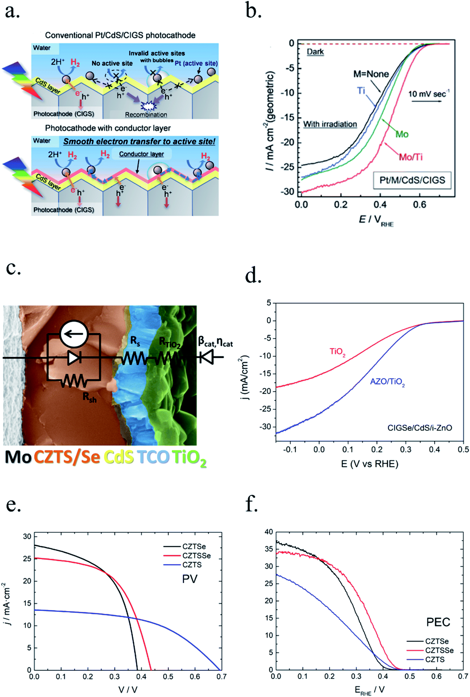 | ||
| Fig. 27 (a) Charge transfer diagram from the n-type CdS layer to HER catalyst particles (top) and with an intermediate metallic conductive film enabling lateral conduction (bottom) and (b) corresponding cyclic voltammograms in 0.5 M Na2SO4, 0.25 M Na2HPO4 and 0.25 M NaH2PO4 (aq.) (pH values adjusted to 6.8 by NaOH addition under AM 1.5G irradiation). Reprinted with permission from (J. Mater. Chem. A, 2015, 3(16), 8300–8307). Copyright (2015) RSC.321 (c) Cross section and equivalent electric circuit of a CZTS/CdS buried heterojunction protected with AZO/TiO2 layers and Pt catalysed. Reprinted with permission from (ACS Appl. Mater. Interfaces, 2018, 10, 13425–13433). Copyright (2018) American Chemical Society.240 (d) Linear sweep voltammograms under 1 sun illumination of CIGSe/CdS/i-ZnO heterojunctions with 300 nm of AZO (blue) or without the underlayer (red), subsequently protected with 100 nm TiO2 ALD layer and 133 mg cm−2 of drop casted Pt as HER. Electrolyte: 0.5 M H2SO4. Reprinted with permission from (Sol. Energy Mater. Sol. Cells, 2016, 158, 184–188). Copyright (2016) Elsevier.241 (e) J(V) curves of CZTSe (black), CZTSSe (red), and CZTS (blue) solar cells as synthesized and (f) polarization curves of the same solar cells protected with TiO2 layers grown at 200 °C and Pt drop-casted on top as HER catalyst. Reprinted with permission from (ACS Appl. Mater. Interfaces, 2018, 10, 13425−13433). Copyright (2018) American Chemical Society.240 | ||
Also, CIGS and CZTS photocathodes are highly sensible to temperature-assisted protection strategies. Higher than 200 °C annealing can alter the vacancy distribution, highly detrimental for final output.240 Significant efforts have been put by our group into understanding the modifications introduced by extra thermal fabrication steps. ALD has been found to allow crystalline-TiO2 deposition temperatures low enough (200 °C) to avoid degradation of CZTSe and CZTSSe-based photoelectrodes, although pure-sulphur CZTS ones photovoltage is severely affected even at 200 °C (Fig. 27e and f). Thus, we can modify the band-gap of the original solar cells from 1.0 to 1.5 eV but some stoichiometries are more challenging to be TiO2-protected. Even so, we can perform the HER with 450 mV photovoltages and 28 mA cm−2 photocurrents stable for over 1 h at 0 V vs. RHE in 0.5 M H2SO4.
Thus, complex buried junction schemes are proven to be readily adapted to PEC with metallic or degenerately doped intermediate layers, confirming the flexibility and advantages of protecting buried junctions.329
8. Cell implementation strategies
During this review focus has been put on front-illuminated metal oxide or protected photoelectrodes, the strategy followed majorly by authors in the field. Although, solar energy can be used to drive an electrochemical reaction in different implementation strategies, with different grade of external control and device complexity.8.1. Photoelectrode configuration
Jacobsson et al.30 have methodically described all the possible transitions from an independent monolithic PEC device, to an electrolyser powered by photovoltaic grid energy. It is depicted in Fig. 28.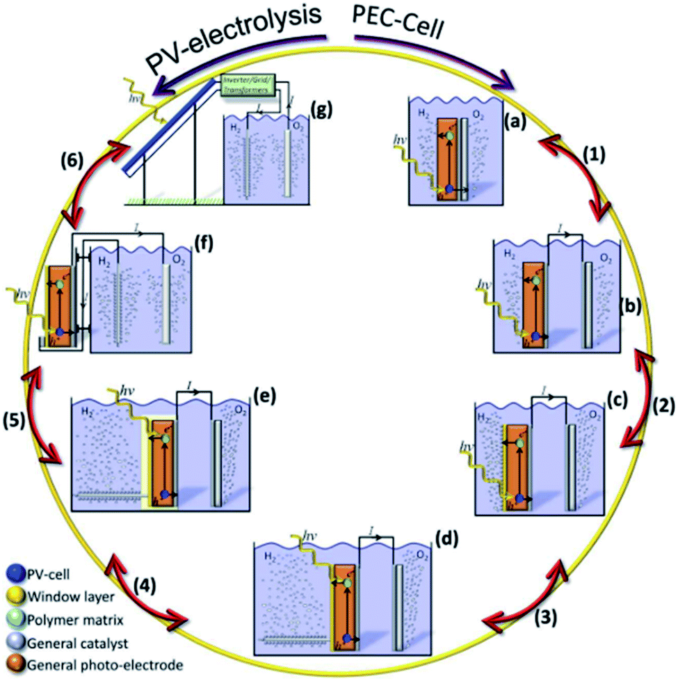 | ||
| Fig. 28 Scheme of the possible transitions from a monolithic PEC device to a photovoltaic-grid powered electrolyser. Reprinted with permission from (Energy Environ. Sci., 2014, 7, 2056). Copyright (2014) RSC.30 | ||
From a monolithic PEC device (a), the first step is separating with an external circuit the second electrode (b). It is shown as a metal, but the second one could be photoactive too, combining photovoltage in a tandem design (its characteristics will be discussed later). The second step is introducing a protective layer between the photoabsorber and the catalyst. In this case, the junction can be formed between the photoabsorber and the electrolyte/catalyst or the layer can intervene in forming a p–n junction (c). A third step is considered if a perpendicular catalyst structure is set on top of the photoabsorber (electrically connected), meanwhile the rest of the surface has the protective layer (d). This way, light can still reach the photoactive semiconductor, meanwhile it is no longer possible to form the depletion with the electrolyte, thus a p–n junction is necessary. Once the vertical catalyst is introduced, next step is directly encapsulating the photoactive part (i.e. by a polymer or glass layer) (e). Once completely isolated, there is no more the need of having the photoactive part inside the electrolyte, and connecting the independent catalyst with a wire to the semiconductor allows freely locating the absorber inside the electrolyte or outside (f). Last step consists of substituting the external photoactive semiconductor with connecting the two remaining catalyst structures with grid photovoltaic (or not) electricity, resulting in a PV-electrolyser setup (g). Jacobsson et al. have implemented several of the mentioned designs with CIGS-based devices.336 As the reader may have realized, the technology readiness is not the same for all configurations:14 both photovoltaics and electrolysers are already commercialised technologies, compared to PEC ones which are still under significant investigation. But as discussed in Section 1, PEC is designed to work at lower current densities, reducing electrochemical overpotentials and enabling higher conversion efficiencies.
Throughout the whole review the vast majority of research has been focused in configurations (b) and (c) of Fig. 28. In-plane electrodes have been discussed in increasing complexity, a path to increment its built-in electric field, its photon absorption, stability and catalytic efficiency.
8.2. Tandem PEC devices
For non-externally biased (unassisted) single light absorber electrodes, only large band gap semiconductors will create enough photovoltage to break the water molecule, meanwhile a dual absorber tandem structure permits absorbing a larger portion of the solar spectra (Fig. 29a and b).117,351 As Hu et al.352 calculated, efficiencies higher than 25% should be obtainable (taking into account earth abundant catalysts overpotential and resistance losses) if band gap semiconductors of ∼1.1 and 1.6–1.8 eV with high performance are found. The short band gap ones are easy to propose, as candidates are already commercial or under development: Si, GaAs, CIGS or perovskites, but the ones with larger band gap still requires more research. Chalcogenides such as CIGS and CZTS have proven the possibility to tune its band gap from 1.0 to 1.6 eV,131,333,344,353,354 and also some perovskites,355 what can help in perfect absorption match for both electrodes to be working in the maximum power point.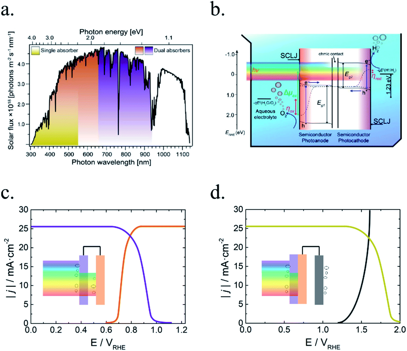 | ||
| Fig. 29 (a) AM 1.5G solar flux as function of photon wavelength and photon energy. The colored areas represent the portion that can be harvested using a single band gap absorber (yellow) or a tandem one (orange + purple) to perform the bias-free water splitting reaction. (b) Tandem monolithic structure with two SCLJ, one front and the other one back illuminated. Reprinted with permission from (J. Phys. Chem. C, 2013, 117, 17879–17893). Copyright (2013) American Chemical Society.351 Cyclic voltammograms simulation of (c) a two front-illuminated photoelectrodes tandem PEC device and its schematics (inset) and (d) a multijunction photoelectrode and a metallic counter electrode with its schematics (inset). | ||
The possible configuration parameters to form a tandem device are vast, and other authors have already performed thoughtful discussions.117,351,352,356,357 For example, both electrodes can be photoactive, combining their performance through the external circuit (Fig. 29c), or one of them can be a multijunction photoelectrode, coupled to a metallic counterelectrode (Fig. 29d). Also, the two photoelectrodes can be connected back-to-back358 (as in Fig. 29b) or both may require frontal illumination (Fig. 29c). Also, either the HER or OER water splitting reaction can be performed in front of the small or large band gap semiconductor, what must be decided based on the protection strategy, stability and catalyst selected. Back-illuminated photoelectrodes are good candidates if the large band gap absorber can be deposited on top of them223,287 and, in principle, do not require transparent protective layers or catalysts, facilitating the search of appropriate low cost and earth abundant materials.
8.3. Electrolyte pH and membranes
Another significant cell design parameter is the electrolyte pH. As it is commonly known, an alkaline electrolyte enhances the OER, whereas an acidic the HER one. In half-cell lab measurements, this is not a problem, but in a full device electrolytes must be either separated with a membrane or the same electrolyte must be chosen for both electrodes. Also, if no gas-separator-membrane is present, detrimental back reactions can happen of dissolved gases and explosive O2/H2 mixtures formed. A highly pure H2 and O2 stream is generated by water splitting, increasing gas products value, thus separating both products is important.17Regarding the catalysts, Pt, Ir, Pd or phosphides such as NiP have 100 times higher H-binding energy in acid than alkaline, and only few earth abundant metallic catalysts such as Ni–Mo have been found relatively effective for HER in alkaline media36 (Fig. 6d). Meanwhile, few expensive catalysts (Ir or Ru) are known to be stable in acid for the OER and all others including earth abundant Ni(Fe)OxHy require basic conditions.359 Also, if same electrolyte is used for both reactions, one of the catalysts will have to drive the water dissociation into H+ and OH− before OER and HER can happen, introducing significant overpotentials, as described in Section 2(e).
Regarding this aspect, bipolar membranes allow different electrolytes to be used in each semi-reaction,359 so acid can be used in the cathode cell side and alkaline in the anode one. These membranes are composed of anion and cation selective layers transporting OH− and H+, respectively, which reacting in the interface. This way no gas or electrolyte crossover is present, and respective pH are maintained allowing the HER and OER to be performed most efficiently. Although, very few studies have been performed in full-cell membrane-divided schemes.
8.4. Cell schemes
Lab-scale measurements, with devices ranging at most few cm2, can ignore current distribution losses due to cell configuration. Although, large scale devices (several tens of cm2) must take in account the current distribution across the photoelectrode to the back contact and ionic conductivity of the liquid, what requires minimizing the distance from one electrode's surface to the other.There are few works which have already faced the emerging series resistances of scale up. For example, Yao et al.360 found a photocurrent loss from 2.2 to 0.74 mA cm−2 at 1.23 V vs. RHE when increasing a BiVO4 photoanode from 2 to 25 cm2, and attributed these losses to electrical resistance of the FTO substrate and non-linear diffusion of reactant ions in the electrolyte. Similar 75% loses caused by substrate resistivity were found by Digler et al. when scaling up LaTiO2N photoanodes from 1 to 40 cm2. Other works, like Lee et al.361 found that introducing an Ag grid deposited on top of the FTO helped reducing the overall sheet resistance and ohmic losses for up to 130 cm2 WO3 photoanodes. Ahmet et al.362 found that, for 50 cm2 BiVO4 photoanodes in neutral electrolyte, Ni grid lines on FTO helped recovering a 10% of the photocurrent lost by scale up, but the main bottleneck was the fast depletion of H+/OH− species. This caused pH changes and potential drops up to 500 mV.
Regarding ionic conductivity of the electrolyte, cell configuration has a key role reducing the species diffusion distance through the electrolyte. Lewis36 identified four possible schemes to implement monolithic “intrinsically safe” (where H2 and O2 are generated in separated compartments) PEC electrodes (Fig. 30a–d). Nano/microwire electrodes grown integrated with the membrane would introduce almost null ionic resistance, as ions must only travel micrometer distances. Some of these include solar concentration of up to 500 times,17 a strategy to minimize device costs, expected to be significantly higher than bare photovoltaics.363 The main drawback of concentration is increasing the current density on the catalytic surface, which will turn into significant extra overpotential, together with the trade-off on an increase of temperature, enhancing electrocatalysis but reducing photovoltaic efficiency. Several other configurations have been analyzed by Minggu et al.,364 for monolithic PEC electrodes or tandem separated ones, set one behind the other or one next to it (Fig. 30e–g).
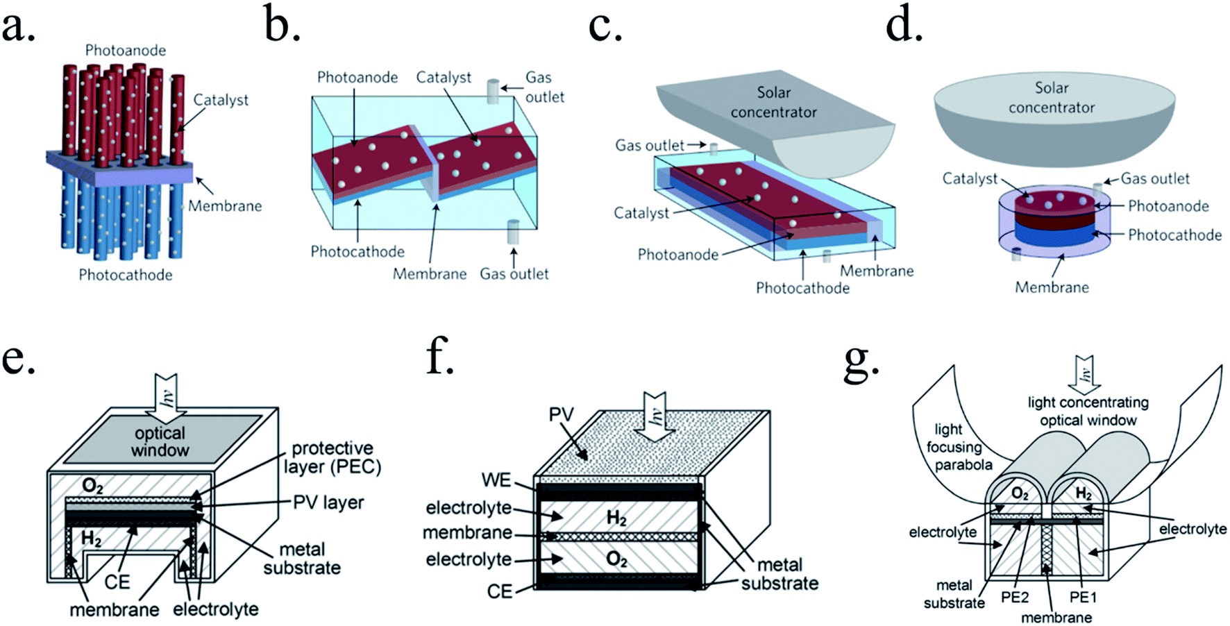 | ||
| Fig. 30 (a–d) Four possible cell schemes of monolithic PEC systems with H2 and O2 generated in separated compartments. Reprinted with permission from (Nat. Nanotechnol., 2016, 11, 1010–1019). Copyright (2016) Springer Nature.36 (e) Non-biased PEC electrode, (f) PV-biased electrodes and (g) laterally-connected tandem electrodes with solar simulator. Reprinted with permission from (Int. J. Hydrog. Energy, 2010, 35, 5233–5244). Copyright (2010) Elsevier.365 | ||
9. Resume, perspective and challenges
Renewable energy sources will eventually be implemented globally, together with energy carriers capable to be distributed and used when necessary. PEC water splitting has demonstrated to produce hydrogen from solar energy and water with significant efficiencies, although this technology is not ready for market implementation due to lack of efficient, stable and scalable photoelectrodes.In this review, the pathway of last decades' investigations on PEC water splitting cells has been discussed. After first discovery of the semiconductor–liquid junction producing few μA cm−2 photocurrents on TiO2, several other semiconductor materials have been tested and modified in the search of an efficient, stable and scalable device, with significant advances obtained. Other metal oxides such as Fe2O3, WO3, BiVO4, or Cu2O have been nanostructured and modified to maximize the built-in electric field to enhance electron–hole separation and transport, together with co-catalyst decoration for a more efficient HER/OER reaction. Even plasmonic nanocrystals have been employed to increase light absorption for energies below the band gap, with impressive doubling the photocurrent. Metal oxide photoelectrodes present good photovoltage and stability in oxidizing environments and are scalable due to earth abundant materials and low cost deposition techniques, but up to now have lacked significant photocurrent generation efficiency.
An alternative approach to overcome this has been adapting short band gap materials such as the ones used for the photovoltaic industry into PEC, mostly III–V semiconductors like GaAs, CdTe or InP, or earth abundant Si, CIGS and CZTS. Semiconductors with 1.0 to 1.8 eV band gap are capable to absorb broad part of the solar spectra, and some of these materials are band gap tunable by composition variations like In/Ga for CIGS and S/Se in CZTS, easing implementation in tandem devices. Although, their main drawback is the instability in aqueous acidic or alkaline electrolytes.
During last decade protective layers have been studied to address this. Metallic films have been deposited on top both as catalysts and to prevent corrosion, but few nanometer thick layers, thin enough to be transparent, were not passivating enough. Tunnel-distances-thick insulator oxides present similar problems, as resistance increases dramatically if more than ∼5 nm are deposited. But protecting short band gap photoabsorbers, containing a buried junction, with semiconductor metal oxide transparent conducting and protective layers several tens of nanometers thick has enabled more than 2000 h stable electrodes, with photocurrents and photovoltages resembling photovoltaic cells. TiO2 and NiO have been the most studied and best performing protective layer materials, the former with Pt or Ni as HER/OER catalysts and the latter being OER catalytic too.
Yet, electron or hole conduction mechanisms across protective layers are still not fully understood. Complex electronic structure in photoabsorber-film interface, across the layer or in the layer-catalyst-electrolyte electrolytic surface are still under discussion. Both for TiO2 and NiO, protective layers, deposition mechanism, precursor or temperature and thus, the nanoscale disorder and electronic structure have presented significant variations among different studies. Moreover, intrinsic stability of these materials when facing thousand-hours scale experiments or intermittent polarization variations should not be directly assumed. Especially in highly oxidizing or reducing electrolytes, as metal oxide protective layers' conductivity relies on cationic or oxygen-deficient electronic structure.
In addition, few works have presented complete PEC cells capable to perform bias free solar water splitting efficiently. Systems based on III–V semiconductors have achieved about 20% solar-to-hydrogen (STH) efficiencies.17 As examples, Cheng et al.366 obtained up to 19.3% conversion efficiency with tandem monolithic GaInAs/GaInP PEC cells TiO2-protected, Licht et al.367 obtained 18% with AlGaAs/Si tandem cells with RuO2/Pt vertical catalysts, and Peharz et al.368 close values with GaInP cells connected to an electrolyser with a polymer electrolyte membrane as separator and under up to 500 suns illumination. Although, III–V semiconductors are grown by very expensive techniques and thus, scalability is difficult due to price and material scarcity.
Some authors have studied reactor schemes and costs, where among several strategies, solar concentration is expected to facilitate the amortization of costly cells, reactors, gas separator membranes and pumping systems.15,363 Meanwhile in recent years, some works have published high efficiencies with earth abundant materials like silicon, oxides or emerging photovoltaic materials with over a 10–14% SHT conversion efficiency.17,369–372 The Department of Energy (D.O.E.) of the United States fixed a road map for PEC water splitting, where meanwhile it has been accomplished for conversion efficiencies, the use of expensive materials and techniques limits the price competitiveness of PEC produced H2.17 PEC water splitting has long been promised with potential of achieving cheap and scalable hydrogen production directly from sun and water, although some authors have questioned this due to the rapid development of photovoltaics and low temperature earth abundant electrolysers, lowering hydrogen production costs.373 We cannot neglect the key role taxes on fossil CO2 could play both in drastically reducing CO2 emissions and facilitating renewable hydrogen implementation.363
In order to implement PEC water splitting at industrial scale, efforts must be put into the fabrication of efficient, stable and scalable photoelectrodes. Stable semiconductor materials fulfilling these requirements have not been found, and although some examples like WSe have shown promising results,374 more research is needed, and the help of computational design of multielement oxides and nitrides will for sure help finding candidates.375
But until a single material fulfilling all requirements is found, the best strategy is protecting photoabsorbers as such used in PV for long term operation. TiO2, NiO or CoOx have been the best performing protective layers so far, fabricated by reactive sputtering, CVD or ALD to minimize pinhole formation. The substitution of high vacuum deposition and time consuming techniques would reduce fabrication costs if pinhole-free layers can be assured. Meanwhile, finding material/electrolyte combinations so the corrosion forms undissolved products must be explored, so pinholes in the protective layer have limited effect to long-term stability of the device.155,238 Using the protective layer as antireflective layer will for sure help in increasing photoelectrodes productivity,172 together with textured silicon surfaces.281
More full cell reactor field tests should be performed during next decade to fully understand complete device stability and degradation mechanisms,376 especially in less-controlled environments, under day/night intermittent operation, temperature changes and mechanical impact caused by bubbling or electrolyte pumping.13,377,378 Regenerative strategies like electrocatalyst re-deposition in dark conditions at night could reduce a constrain, increasing available material candidates.306,379,380 For a large scale deployment of water splitting, which will consume significant volume in a clean water scarcity scenario, seawater must also be studied as water-source.381,382
Although some authors have claimed demonstration or early-stage commercial devices would be possible with noble metals if cost-efficiency is matched, earth abundant alternatives must be researched for large scale deployment.13 Bias-free tandem cells will require medium band-gap semiconductors to be coupled with short ones, and chalcogenides or perovskites (band gap tunable by composition control) have shown promising results for solar cells.131 In addition, finding earth abundant transparent and conductive catalysts, especially inexistent for OER in acid and HER in alkaline, would reduce the constrains on selecting electrolytes and reactions performed on each side. Protective layers with superficial energetics prone to enhance HER or OER catalysis would simplify even more the structures. Some of the most promising earth abundant candidates have been Ni-based catalysts for OER and MoSx for HER. NiO protective layers surface incorporates Fe and forms Ni(Fe)OOH in alkaline media, one of the most efficient earth abundant OER catalysts,172 or MoS2 protective and transparent layers have been recently grown and reported stable in acid with good HER catalysis.307
Furthermore, during last decade some authors have implemented photoelectrochemistry for other reactions besides water splitting. Carbon dioxide reduction reaction (CO2RR) is far more complex than water splitting, but enables the possibility to extract the greenhouse gas CO2 from the atmosphere and turn it into a reusable fuel or chemical. Commercial products like methane or ethanol production from CO2 reduction have been studied, which could directly be incorporated into the actual carbon-based fossil fuels marked, and several other molecules are possible with appropriate catalysts. The possibility of obtaining liquid products is especially interesting, as highly simplifies distribution and storage (some of the main drawbacks for H2 as energy vector implementation). Main challenges for CO2 reduction are finding appropriate catalysts and stable semiconductors to be placed in direct contact with the reaction, as the higher required reductive potentials (>1 V) enhance materials corrosion.375,383 Electrochemical reduction of organics such as ethanol have also been studied as hydrogen sources where lower cell potential is needed.384 Implementing photoelectrodes to redox-flow batteries has enabled the concept of “photobattery”, for example with vanadium as electrolyte.385,386 For sure the development of PEC water splitting will help with identifying and adapting photoelectrodes for other electrochemical reactions.
Conflicts of interest
There are no conflicts to declare.Acknowledgements
Authors acknowledge Generalitat de Catalunya for financial support through the CERCA Programme, M2E (2014SGR1638). IREC also acknowledges additional support by the European Regional Development Funds (ERDF, FEDER) and by MINECO coordinated projects MAT2014-59961-C2, ENE2016-80788-C5-5-R and ENE2017-85087-C3. C. R. acknowledges MINECO for his FPI grant (BES-2015-071618).Notes and references
- R. Heinberg and D. Fridley, Our Renewable Future, Island Press, 2016 Search PubMed.
- J. M. Godoy, Rev. Virtual Quim., 2018, 10, 1733–1757 CrossRef.
- G. D. Berry, A. D. Pasternak, G. D. Rambach, J. R. Smith and R. N. Schock, Energy, 1996, 21, 289–303 CrossRef CAS.
- A. Fujishima and K. Honda, Nature, 1972, 238, 37–38 CrossRef CAS PubMed.
- Z. Li, J. Feng, S. Yan and Z. Zou, Nano Today, 2015, 1–19 Search PubMed.
- A. J. Bard, J. Photochem., 1979, 10, 59–75 CrossRef CAS.
- D. Tafalla and P. Salvador, J. Electroanal. Chem., 1989, 270(1–2), 285–295 CrossRef CAS.
- K. J. Hartig and N. Getoff, Int. J. Hydrogen Energy, 1986, 11(12), 773–781 CrossRef CAS.
- M. K. Carpenter and D. A. Corrigan, J. Electrochem. Soc., 1989, 136, 1022 CrossRef CAS.
- A. Heller, E. Aharon-Shalom, W. A. Bonner and B. Miller, J. Am. Chem. Soc., 1982, 104, 6942–6948 CrossRef CAS.
- L. A. Harris, J. Electrochem. Soc., 1977, 124, 1511 CrossRef CAS.
- H. Morisaki, H. Ono, H. Dohkoshi and K. Yazawa, Jpn. J. Appl. Phys., 1980, 19, L148–L150 CrossRef CAS.
- J. R. McKone, N. S. Lewis and H. B. Gray, Chem. Mater., 2014, 26, 407–414 CrossRef CAS.
- S. Ardo, D. Fernandez Rivas, M. A. Modestino, V. Schulze Greiving, F. F. Abdi, E. Alarcon-Llado, V. Artero, K. E. Ayers, C. Battaglia, J.-P. Becker, D. Bederak, A. Berger, F. Buda, E. Chinello, B. Dam, V. Di Palma, T. Edvinsson, K. Fujii, H. J. G. E. Gardeniers, H. Geerlings, S. M. Hosseini Hashemi, S. Haussener, F. A. Houle, J. Huskens, B. D. James, K. Konrad, A. Kudo, P. P. Kunturu, D. Lohse, B. Mei, E. L. Miller, G. Moere, J. Muller, K. L. Orchard, T. E. Rosser, F. H. Saadi, J.-W. Schüttauf, B. J. Seger, S. W. Sheehan, W. A. Smith, J. Spurgeon, M. H. Tang, R. van de Krol, P. C. K. Vesborg and P. Westerik, Energy Environ. Sci., 2018, 11(10), 2768–2783 RSC.
- M. R. Shaner, H. A. Atwater, N. S. Lewis and E. W. McFarland, Energy Environ. Sci., 2016, 9, 2354–2371 RSC.
- A. Rothschild and H. Dotan, ACS Energy Lett., 2017, 2, 45–51 CrossRef CAS.
- J. W. Ager, M. R. Shaner, K. A. Walczak, I. D. Sharp and S. Ardo, Energy Environ. Sci., 2015, 8, 2811–2824 RSC.
- M. Görlin, P. Chernev, J. F. De Araújo, T. Reier, S. Dresp, B. Paul, R. Krähnert, H. Dau and P. Strasser, J. Am. Chem. Soc., 2016, 138, 5603–5614 CrossRef PubMed.
- A. Dutta and N. Pradhan, J. Phys. Chem. Lett., 2016, 144–152 Search PubMed.
- J. D. Benck, T. R. Hellstern, J. Kibsgaard, P. Chakthranont and T. F. Jaramillo, ACS Catal., 2014, 4, 3957–3971 CrossRef CAS.
- Y. Yan, B. Xia, Z. Xu and X. Wang, ACS Catal., 2014, 4, 1693–1705 CrossRef CAS.
- M. Gong and H. Dai, Nano Res., 2014, 8, 23–39 CrossRef.
- L. Trotochaud, J. K. Ranney, K. N. Williams and S. W. Boettcher, J. Am. Chem. Soc., 2012, 134, 17253–17261 CrossRef CAS PubMed.
- W. Sheng, H. A. Gasteiger and Y. Shao-Horn, J. Electrochem. Soc., 2010, 157, B1529 CrossRef CAS.
- S. Trasatti, Pure Appl. Chem., 1986, 58, 955–966 CAS.
- H. Li, S. Chen, Y. Zhang, Q. Zhang, Q. Zhang, X. Jia, L. Gu, X. Sun, L. Song and X. Wang, Nat. Commun., 2018, 9, 1–12 CrossRef PubMed.
- Z. Y. Yu, C. C. Lang, M. R. Gao, Y. Chen, Q. Q. Fu, Y. Duan and S. H. Yu, Energy Environ. Sci., 2018, 11, 1890–1897 RSC.
- H. Helmholtz, Ann. Phys. Chem., 1879, 243, 337–382 CrossRef.
- O. Newman and K. E. Thomas-Alyea, Electrochemical Systems, 2004 Search PubMed.
- T. J. Jacobsson, V. Fjällström, M. Edoff and T. Edvinsson, Energy Environ. Sci., 2014, 7, 2056 RSC.
- A. B. Murphy, P. R. F. Barnes, L. K. Randeniya, I. C. Plumb, I. E. Grey, M. D. Horne and J. A. Glasscock, Int. J. Hydrogen Energy, 2006, 31, 1999–2017 CrossRef CAS.
- Z. Chen, H. N. Dinh and E. Miller, Photoelectrochemical Water Splitting - Standards, Experimental Methods, and Protocols, Springer, 2013 Search PubMed.
- C. Jiang, S. J. A. Moniz, A. Wang, T. Zhang and J. Tang, Chem. Soc. Rev., 2017, 46, 4645–4660 RSC.
- W. A. Smith, I. D. Sharp, N. C. Strandwitz and J. Bisquert, Energy Environ. Sci., 2015, 8, 2851–2862 RSC.
- Y. Yang, S. Niu, D. Han, T. Liu, G. Wang and Y. Li, Adv. Energy Mater., 2017, 7, 1–26 Search PubMed.
- N. S. Lewis, Nat. Nanotechnol., 2016, 11, 1010–1019 CrossRef CAS PubMed.
- S. Chen and L. W. Wang, Chem. Mater., 2012, 24, 3659–3666 CrossRef CAS.
- T. Berger, D. Monllor-Satoca, M. Jankulovska, T. Lana-Villarreal and R. Gómez, ChemPhysChem, 2012, 13, 2824–2875 CrossRef CAS PubMed.
- J. Wang, X. Liu, R. Li, P. Qiao, L. Xiao and J. Fan, Catal. Commun., 2012, 19, 96–99 CrossRef CAS.
- M. Jankulovska, T. Berger, S. S. Wong, R. Gómez and T. Lana-Villarreal, ChemPhysChem, 2012, 13, 3008–3017 CrossRef CAS PubMed.
- J. Fan, C. Fàbrega, R. R. Zamani, Y. Hao, A. Parra, T. Andreu, J. Arbiol, G. Boschloo, A. Hagfeldt, J. R. Morante and A. Cabot, ACS Appl. Mater. Interfaces, 2013, 5, 9872–9877 CrossRef CAS PubMed.
- J. Sá, P. Friedli, R. Geiger, P. Lerch, M. H. Rittmann-Frank, C. J. Milne, J. Szlachetko, F. G. Santomauro, J. A. van Bokhoven, M. Chergui, M. J. Rossi and H. Sigg, Analyst, 2013, 138, 1966 RSC.
- J. Y. Kim, G. Magesh, D. H. Youn, J. W. Jang, J. Kubota, K. Domen and J. S. Lee, Sci. Rep., 2013, 3, 1–8 Search PubMed.
- P. Dias, A. Vilanova, T. Lopes, L. Andrade and A. Mendes, Nano Energy, 2016, 23, 70–79 CrossRef CAS.
- K. Sivula, F. Le Formal and M. Grätzel, ChemSusChem, 2011, 4, 432–449 CrossRef CAS PubMed.
- Y. Wei, L. Ke, J. Kong, H. Liu, Z. Jiao, X. Lu, H. Du and X. W. Sun, Nanotechnology, 2012, 23(23), 235401 CrossRef PubMed.
- B. S. Wang, R. Y. Li, Z. Y. Zhang, Xing-Wang, X. L. Wu, G. A. Cheng and R. T. Zheng, Catal. Today, 2019, 321–322, 100–106 CrossRef CAS.
- J. Y. Zheng, G. Song, J. Hong, T. K. Van, A. U. Pawar, D. Y. Kim, C. W. Kim, Z. Haider and Y. S. Kang, Cryst. Growth Des., 2014, 14, 6057–6066 CrossRef CAS.
- J. Su, X. Feng, J. D. Sloppy, L. Guo and C. A. Grimes, Nano Lett., 2011, 11, 203–208 CrossRef CAS PubMed.
- C. Fàbrega, S. Murcia-López, D. Monllor-Satoca, J. D. Prades, M. D. Hernández-Alonso, G. Penelas, J. R. Morante and T. Andreu, Appl. Catal., B, 2016, 189, 133–140 CrossRef.
- T. W. Kim and K.-S. Choi, J. Phys. Chem. Lett., 2016, 7, 447–451 CrossRef CAS PubMed.
- J. A. Seabold and K. S. Choi, J. Am. Chem. Soc., 2012, 134, 2186–2192 CrossRef CAS PubMed.
- F. F. Abdi and R. Van De Krol, J. Phys. Chem. C, 2012, 116, 9398–9404 CrossRef CAS.
- S. P. Berglund, D. W. Flaherty, N. T. Hahn, A. J. Bard and C. B. Mullins, J. Phys. Chem. C, 2011, 115, 3794–3802 CrossRef CAS.
- C. Hu, K. Chu, Y. Zhao and W. Y. Teoh, ACS Appl. Mater. Interfaces, 2014, 6, 18558–18568 CrossRef CAS PubMed.
- R. Wick and S. D. Tilley, J. Phys. Chem. C, 2015, 119, 26243–26257 CrossRef CAS.
- A. J. Bard, J. Electrochem. Soc., 1977, 1706–1710 CrossRef CAS.
- H. Gerischer, J. Electroanal. Chem., 1977, 82, 133–143 CrossRef CAS.
- J. Luo, L. Steier, M. K. Son, M. Schreier, M. T. Mayer and M. Grätzel, Nano Lett., 2016, 16, 1848–1857 CrossRef CAS PubMed.
- J. Li and N. Wu, Catal. Sci. Technol., 2015, 5, 1360 RSC.
- F. M. Toma, J. K. Cooper, V. Kunzelmann, M. T. McDowell, J. Yu, D. M. Larson, N. J. Borys, C. Abelyan, J. W. Beeman, K. M. Yu, J. Yang, L. Chen, M. R. Shaner, J. Spurgeon, F. A. Houle, K. A. Persson and I. D. Sharp, Nat. Commun., 2016, 7, 1–11 Search PubMed.
- Y. J. Jang, Y. Bin Park, H. E. Kim, Y. H. Choi, S. H. Choi and J. S. Lee, Chem. Mater., 2016, 28, 6054–6061 CrossRef CAS.
- J. Seo, H. Nishiyama, T. Yamada and K. Domen, Angew. Chem., Int. Ed., 2018, 57, 8396–8415 CrossRef CAS PubMed.
- R. Abe, M. Higashi and K. Domen, J. Am. Chem. Soc., 2010, 132, 11828–11829 CrossRef CAS PubMed.
- S. Akiyama, M. Nakabayashi, N. Shibata, T. Minegishi, Y. Asakura, M. Abdulla-Al-Mamun, T. Hisatomi, H. Nishiyama, M. Katayama, T. Yamada and K. Domen, Small, 2016, 12, 5468–5476 CrossRef CAS PubMed.
- W. J. Yin, H. Tang, S. H. Wei, M. M. Al-Jassim, J. Turner and Y. Yan, Phys. Rev. B: Condens. Matter Mater. Phys., 2010, 82, 1–6 Search PubMed.
- X. Huang, X. Gao, Q. Xue, C. Wang, R. Zhang, Y. Gao and Z. Han, Dalton Trans., 2020, 49, 2184–2189 RSC.
- G. Wang, X. Xiao, W. Li, Z. Lin, Z. Zhao, C. Chen, C. Wang, Y. Li, X. Huang, L. Miao, C. Jiang, Y. Huang and X. Duan, Nano Lett., 2015, 15, 4692–4698 CrossRef CAS PubMed.
- G. Wang, H. Wang, Y. Ling, Y. Tang, X. Yang, R. C. Fitzmorris, C. Wang, J. Z. Zhang and Y. Li, Nano Lett., 2011, 11, 3026–3033 CrossRef CAS PubMed.
- C. Yang, Z. Wang, T. Lin, H. Yin, X. Lü, D. Wan, T. Xu, C. Zheng, J. Lin, F. Huang, X. Xie and M. Jiang, J. Am. Chem. Soc., 2013, 135, 17831–17838 CrossRef CAS PubMed.
- C. Fàbrega, T. Andreu, F. Güell, J. D. Prades, S. Estradé, J. M. Rebled, F. Peiró and J. R. Morante, Nanotechnology, 2011, 22, 235403 CrossRef PubMed.
- C. Ros, C. Fabrega, D. Monllor-Satoca, M. D. Hernández-Alonso, G. Penelas-Pérez, J. R. Morante and T. Andreu, J. Phys. Chem. C, 2018, 122, 3295–3304 CrossRef CAS.
- F. Wang, C. Di Valentin and G. Pacchioni, J. Phys. Chem. C, 2012, 116, 8901–8909 CrossRef CAS.
- F. Wang, C. DiValentin and G. Pacchioni, ChemCatChem, 2012, 4, 476–478 CrossRef CAS.
- J. N. Hart, M. Cutini and N. L. Allan, Energy Procedia, 2014, 60, 32–36 CrossRef CAS.
- S. B. A. Hamid, S. J. Teh and C. W. Lai, Catalysts, 2017, 7, 93 CrossRef.
- M. Wang, F. Ren, J. Zhou, G. Cai, L. Cai, Y. Hu, D. Wang, Y. Liu, L. Guo and S. Shen, Sci. Rep., 2015, 5, 12925 CrossRef CAS PubMed.
- Y. S. Chen and P. V. Kamat, J. Am. Chem. Soc., 2014, 136, 6075–6082 CrossRef CAS PubMed.
- F. X. Xiao, S. F. Hung, J. Miao, H. Y. Wang, H. Yang and B. Liu, Small, 2015, 11, 554–567 CrossRef CAS PubMed.
- Z. Zhang, L. Zhang, M. N. Hedhili, H. Zhang and P. Wang, Nano Lett., 2013, 13, 14–20 CrossRef CAS PubMed.
- T. Wang, Z. Luo, C. Li and J. Gong, Chem. Soc. Rev., 2014, 43, 7469–7484 RSC.
- Q. Kang, J. Cao, Y. Zhang, L. Liu, H. Xu and J. Ye, J. Mater. Chem. A, 2013, 1, 5766 RSC.
- C. Fàbrega, F. Hernández-Ramírez, J. Daniel Prades, R. Jiménez-Díaz, T. Andreu and J. Ramon Morante, Nanotechnology, 2010, 21, 445703 CrossRef PubMed.
- Y. Yang, L. C. Kao, Y. Liu, K. Sun, H. Yu, J. Guo, S. Y. H. Liou and M. R. Hoffmann, ACS Catal., 2018, 8, 4278–4287 CrossRef CAS PubMed.
- C. Fàbrega, T. Andreu, A. Tarancón, C. Flox, A. Morata, L. Calvo-Barrio and J. R. Morante, Int. J. Hydrogen Energy, 2013, 38, 2979–2985 CrossRef.
- J. M. Wu, T. W. Zhang, Y. W. Zeng, S. Hayakawa, K. Tsuru and A. Osaka, Langmuir, 2005, 21, 6995–7002 CrossRef CAS PubMed.
- C. Fàbrega, D. Monllor-Satoca, S. Ampudia, A. Parra, T. Andreu and J. R. Morante, J. Phys. Chem. C, 2013, 117, 20517–20524 CrossRef.
- P. M. Rao, L. Cai, C. Liu, I. S. Cho, C. H. Lee, J. M. Weisse, P. Yang and X. Zheng, Nano Lett., 2014, 14, 1099–1105 CrossRef CAS PubMed.
- X. Yang, R. Liu, Y. Lei, P. Li, K. Wang, Z. Zheng and D. Wang, ACS Appl. Mater. Interfaces, 2016, 8, 16476–16485 CrossRef CAS PubMed.
- P. Tang, H. Xie, C. Ros, L. Han, M. Biset-Peiró, Y. He, W. Kramer, A. P. Rodríguez, E. Saucedo, J. R. Galán-Mascarós, T. Andreu, J. R. Morante and J. Arbiol, Energy Environ. Sci., 2017, 10, 2124–2136 RSC.
- G. K. Mor, O. K. Varghese, R. H. T. Wilke, S. Sharma, K. Shankar, T. J. Latempa, K. Choi and C. A. Grimes, Nano Lett., 2008, 8, 1906–1911 CrossRef CAS PubMed.
- A. Paracchino, V. Laporte, K. Sivula, M. Grätzel and E. Thimsen, Nat. Mater., 2011, 10, 456–461 CrossRef CAS PubMed.
- M. Zhou, J. Bao, Y. Xu, J. Zhang, J. Xie, M. Guan, C. Wang, L. Wen, Y. Lei and Y. Xie, ACS Nano, 2014, 8, 7088–7098 CrossRef CAS PubMed.
- T. Lopes, L. Andrade, F. Le Formal, M. Gratzel, K. Sivula and A. Mendes, Phys. Chem. Chem. Phys., 2014, 16, 16515–16523 RSC.
- B. Klahr, S. Gimenez, F. Fabregat-Santiago, J. Bisquert and T. W. Hamann, Energy Environ. Sci., 2012, 5, 7626 RSC.
- Y. Qiu, W. Liu, W. Chen, G. Zhou, P. C. Hsu, R. Zhang, Z. Liang, S. Fan, Y. Zhang and Y. Cui, Sci. Adv., 2016, 2(6), e1501764 CrossRef PubMed.
- S. Cho, J. W. Jang, K. H. Lee and J. S. Lee, APL Mater., 2014, 2, 010703 CrossRef.
- J. A. Glasscock, P. R. F. Barnes, I. C. Plumb and N. Savvides, J. Phys. Chem. C, 2007, 111, 16477–16488 CrossRef CAS.
- Y. Hu, A. Kleiman-Shwarsctein, A. J. Forman, D. Hazen, J. Park and E. W. McFarland, Chem. Mater., 2008, 20, 3803–3805 CrossRef CAS.
- A. Kleiman-Shwarsctein, Y. S. Hu, A. J. Forman, G. D. Stucky and E. W. McFarland, J. Phys. Chem. C, 2008, 112, 15900–15907 CrossRef CAS.
- J. Prakash, U. Prasad, X. Shi, X. Peng, B. Azeredo and A. M. Kannan, J. Power Sources, 2020, 448, 227418 CrossRef CAS.
- P. Y. Tang, L. J. Han, F. S. Hegner, P. Paciok, M. Biset-Peiró, H. C. Du, X. K. Wei, L. Jin, H. B. Xie, Q. Shi, T. Andreu, M. Lira-Cantú, M. Heggen, R. E. Dunin-Borkowski, N. López, J. R. Galán-Mascarós, J. R. Morante and J. Arbiol, Adv. Energy Mater., 2019, 9, 1–11 Search PubMed.
- J. Wang, J. L. Waters, P. Kung, S. M. Kim, J. T. Kelly, L. E. McNamara, N. I. Hammer, B. C. Pemberton, R. H. Schmehl, A. Gupta and S. Pan, ACS Appl. Mater. Interfaces, 2017, 9, 381–390 CrossRef CAS PubMed.
- Q. Shi, S. Murcia-López, P. Tang, C. Flox, J. R. Morante, Z. Bian, H. Wang and T. Andreu, ACS Catal., 2018, 8, 3331–3342 CrossRef CAS.
- S. K. Pilli, T. E. Furtak, L. D. Brown, T. G. Deutsch, J. A. Turner and A. M. Herring, Energy Environ. Sci., 2011, 4, 5028–5034 RSC.
- F. F. Abdi, L. Han, A. H. M. Smets, M. Zeman, B. Dam and R. Van De Krol, Nat. Commun., 2013, 4, 1–7 Search PubMed.
- G. Wang, Y. Ling, X. Lu, F. Qian, Y. Tong, J. Z. Zhang, V. Lordi, C. Rocha Leao and Y. Li, J. Phys. Chem. C, 2013, 117, 10957–10964 CrossRef CAS.
- Y. Hermans, S. Murcia-López, A. Klein and W. Jaegermann, ACS Energy Lett., 2019, 4, 2522–2528 CrossRef CAS.
- M. Barroso, C. A. Mesa, S. R. Pendleburya, A. J. Cowana, T. Hisatomi, K. Sivula, M. Grätzelb, D. R. Kluga, J. R. Durrant, S. R. Pendlebury, A. J. Cowan, T. Hisatomi, K. Sivula, M. Gratzel, D. R. Klug and J. R. Durrant, Proc. Natl. Acad. Sci. U. S. A., 2012, 109, 1–89 CrossRef PubMed.
- T. Hisatomi, F. Le Formal, M. Cornuz, J. Brillet, N. Tétreault, K. Sivula and M. Grätzel, Energy Environ. Sci., 2011, 4, 2512–2515 RSC.
- X. Yang, R. Liu, C. Du, P. Dai, Z. Zheng and D. Wang, ACS Appl. Mater. Interfaces, 2014, 6, 12005–12011 CrossRef CAS PubMed.
- R. Liu, Z. Zheng, J. Spurgeon and X. Yang, Energy Environ. Sci., 2014, 7, 2504–2517 RSC.
- Y. Hermans, S. Murcia-López, A. Klein, R. Van De Krol, T. Andreu, J. R. Morante, T. Toupance and W. Jaegermann, Phys. Chem. Chem. Phys., 2019, 21, 5086–5096 RSC.
- Y. Makimizu, J. E. Yoo, M. Poornajar, N. T. Nguyen, H. J. Ahn, I. Hwang, S. Kment and P. Schmuki, J. Mater. Chem. A, 2020, 8, 1315–1325 RSC.
- C. C. L. McCrory, S. Jung, I. M. Ferrer, S. M. Chatman, J. C. Peters and T. F. Jaramillo, J. Am. Chem. Soc., 2015, 137, 4347–4357 CrossRef CAS PubMed.
- H. Osgood, S. V. Devaguptapu, H. Xu, J. Cho and G. Wu, Nano Today, 2016, 11, 601–625 CrossRef CAS.
- P. Peerakiatkhajohn, J.-H. Yun, S. Wang and L. Wang, J. Photonics Energy, 2016, 7, 012006 CrossRef.
- M. S. Burke, L. J. Enman, A. S. Batchellor, S. Zou and S. W. Boettcher, Chem. Mater., 2015, 27, 7549–7558 CrossRef CAS.
- M. S. Faber and S. Jin, Energy Environ. Sci., 2014, 7, 3519–3542 RSC.
- S. D. Tilley, M. Schreier, J. J. J. Azevedo, M. Stefik and M. Graetzel, Adv. Funct. Mater., 2014, 24, 303–311 CrossRef CAS.
- C. G. Morales-Guio, S. D. Tilley, H. Vrubel, M. Grätzel and X. Hu, Nat. Commun., 2014, 5, 1–7 Search PubMed.
- N. Rahimi, R. A. Pax and E. M. A. Gray, Prog. Solid State Chem., 2016, 44, 86–105 CrossRef CAS.
- Y. Duan, S. Zhou, Z. Chen, J. Luo, M. Zhang, F. Wang, T. Xu and C. Wang, Catal. Sci. Technol., 2018, 8, 1395–1403 RSC.
- D. K. Zhong, M. Cornuz, K. Sivula, M. Grätzel and D. R. Gamelin, Energy Environ. Sci., 2011, 4, 1759–1764 RSC.
- J. Su, L. Guo, N. Bao and C. A. Grimes, Nano Lett., 2011, 11, 1928–1933 CrossRef CAS PubMed.
- M. R. Shaner, K. T. Fountaine, S. Ardo, R. H. Coridan, H. A. Atwater and N. S. Lewis, Energy Environ. Sci., 2014, 7, 779–790 RSC.
- R. H. Coridan, K. A. Arpin, B. S. Brunschwig, P. V. Braun and N. S. Lewis, Nano Lett., 2014, 14, 2310–2317 CrossRef CAS PubMed.
- Y. Zhao, P. Westerik, R. Santbergen, E. Zoethout, H. Gardeniers and A. Bieberle-Hütter, Adv. Funct. Mater., 2020, 1909157, 1–10 Search PubMed.
- C. Liu, J. Tang, H. M. Chen, B. Liu and P. Yang, Nano Lett., 2013, 13, 2989–2992 CrossRef CAS PubMed.
- S. Y. Noh, K. Sun, C. Choi, M. Niu, M. Yang, K. Xu, S. Jin and D. Wang, Nano Energy, 2013, 2, 351–360 CrossRef CAS.
- A. Polman, M. Knight, E. C. Garnett, B. Ehrler, W. C. Sinke, R. Summary, A. Polman, M. Knight, E. C. Garnett, B. Ehrler and W. C. Sinke, Science, 2016, 352, 307 CrossRef CAS PubMed.
- A. G. Aberle, Prog. Photovolt: Res. Appl., 2000, 8, 473–487 CrossRef CAS.
- Y. Lee, C. Park, N. Balaji, Y.-J. Lee and V. A. Dao, Isr. J. Chem., 2015, 55, 1050–1063 CrossRef CAS.
- T. Saga, NPG Asia Mater., 2010, 2, 96–102 CrossRef.
- B. C. Huayhuas-Chipana, J. C. M. Gomero and M. D. P. T. Sotomayor, J. Braz. Chem. Soc., 2014, 25, 1737–1745 CAS.
- L. F. Huang, M. J. Hutchison, R. J. Santucci, J. R. Scully and J. M. Rondinelli, J. Phys. Chem. C, 2017, 121, 9782–9789 CrossRef CAS.
- R. Parsons, J. Electroanal. Chem. Interfacial Electrochem., 1967, 13, 471 Search PubMed.
- P. Acevedo-Pena, J. Vazquez-Arenas, R. Cabrera-Sierra, L. Lartundo-Rojas and I. Gonzalez, J. Electrochem. Soc., 2013, 160, C277–C284 CrossRef CAS.
- S. Chen, D. Huang, P. Xu, W. Xue, L. Lei, M. Cheng, R.-Z. Wang, X. Liu and R. Deng, Semiconductor-based photocatalysts for photocatalytic and photoelectrochemical water splitting: will we stop with photocorrosion?, Royal Society of Chemistry, 2020 Search PubMed.
- N. C. Strandwitz, D. J. Comstock, R. L. Grimm, A. C. Nichols-Nielander, J. Elam and N. S. Lewis, J. Phys. Chem. C, 2013, 117, 4931–4936 CrossRef CAS.
- K. Sun, X. Pang, S. Shen, X. Qian, J. S. Cheung and D. Wang, Nano Lett., 2013, 13, 2064–2072 CrossRef CAS PubMed.
- P. A. Nikolaychuk, Silicon, 2014, 6, 109–116 CrossRef CAS.
- E. Kim and K. Osseo-Asare, Hydrometallurgy, 2012, 127–128, 178–186 CrossRef CAS.
- S. Milenkovic, V. Dalbert, R. Marinkovic and A. W. Hassel, Corros. Sci., 2009, 51, 1490–1495 CrossRef CAS.
- D. Bae, S. Shayestehaminzadeh, E. B. Thorsteinsson, T. Pedersen, O. Hansen, B. Seger, P. C. K. Vesborg, S. Ólafsson and I. Chorkendorff, Sol. Energy Mater. Sol. Cells, 2016, 144, 758–765 CrossRef CAS.
- H. J. Lewerenz, K. Skorupska, A. G. Muñoz, T. Stempel, N. Nüsse, M. Lublow, T. Vo-Dinh and P. Kulesza, Electrochim. Acta, 2011, 56, 10726–10736 CrossRef CAS.
- I. Z. Awan, A. Q. Khan, I. Z. Awan, A. Q. Khan, E. Nationale and S. De Chimie, J. Chem. Soc. Pak., 2018, 40, 602–655 CAS.
- B. Beverskog and I. Puigdomenech, Corros. Sci., 1997, 39, 107–114 CrossRef CAS.
- R. Buckle and S. Roy, Sep. Purif. Technol., 2008, 62, 86–96 CrossRef CAS.
- S. Geiger, O. Kasian, A. M. Mingers, K. J. J. Mayrhofer and S. Cherevko, Sci. Rep., 2017, 7, 3–9 CrossRef PubMed.
- S. W. F. M. Van Hövell Tot Westerflier, J. J. M. Binsma, H. N. Stein and C. Vandecasteele, J. Radioanal. Nucl. Chem., 1987, 111, 305–317 CrossRef.
- D. Tromans, J. Electrochem. Soc., 2009, 156, C367 CrossRef CAS.
- A. G. Voloshchuk and N. I. Tsipishchuk, Inorg. Mater., 2002, 38, 1114–1116 CrossRef CAS.
- B. Fotouhi, R. Triboulet and M. Etman, J. Electroanal. Chem. Interfacial Electrochem., 1985, 195, 425–430 CrossRef CAS.
- D. Bae, B. Seger, P. C. K. Vesborg, O. Hansen and I. Chorkendorff, Chem. Soc. Rev., 2017, 46, 1933–1954 RSC.
- B. Yan, G. Yue, J. Yang and S. Guha, 19th Int. Work. Act. Flatpanel Displays Devices - TFT Technol. FPD Mater., 2012, vol. 108, pp. 67–70 Search PubMed.
- A. Guerrero and J. Bisquert, Curr. Opin. Electrochem., 2017, 2, 144–147 CrossRef CAS.
- W. Wang, M. Xu, X. Xu, W. Zhou and Z. Shao, Angew. Chem., Int. Ed., 2020, 59, 136–152 CrossRef CAS PubMed.
- D. Kim, D.-K. Lee, S. M. Kim, W. Park and U. Sim, Materials, 2020, 13, 210 CrossRef PubMed.
- A. Guerrero, M. Haro, S. Bellani, M. R. Antognazza, L. Meda, S. Gimenez and J. Bisquert, Energy Environ. Sci., 2014, 7, 3666–3673 RSC.
- P. Xu, N. S. McCool and T. E. Mallouk, Nano Today, 2017, 14, 42–58 CrossRef CAS.
- J. Brillet, J.-H. Yum, M. Cornuz, T. Hisatomi, R. Solarska, J. Augustynski, M. Graetzel and K. Sivula, Nat. Photonics, 2012, 6, 824–828 CrossRef CAS.
- A. Bansal and N. S. Lewis, J. Phys. Chem. B, 1998, 102, 4058–4060 CrossRef CAS.
- A. Bansal, X. Li, I. Lauermann, N. S. Lewis, S. I. Yi and W. H. Weinberg, J. Am. Chem. Soc., 1996, 118, 7225–7226 CrossRef CAS.
- S. Hu, N. S. Lewis, J. W. Ager, J. Yang, J. R. McKone and N. C. Strandwitz, J. Phys. Chem. C, 2015, 119, 24201–24228 CrossRef CAS.
- M. F. Lichterman, K. Sun, S. Hu, X. Zhou, M. T. McDowell, M. R. Shaner, M. H. Richter, E. J. Crumlin, A. I. Carim, F. H. Saadi, B. S. Brunschwig and N. S. Lewis, Catal. Today, 2016, 262, 11–23 CrossRef CAS.
- R. P. Feynman, Miniaturization, 1960, 282–296 Search PubMed.
- F. Lévy, Ref. Modul. Mater. Sci. Mater. Eng., 2016, pp. 1–16 Search PubMed.
- M. G. Kast, L. J. Enman, N. J. Gurnon, A. Nadarajah and S. W. Boettcher, ACS Appl. Mater. Interfaces, 2014, 6, 22830–22837 CrossRef CAS PubMed.
- G. Oskam, J. G. Long, A. Natarajan and P. C. Searson, J. Phys. D: Appl. Phys., 1998, 1927–1949 CrossRef CAS.
- K. Sun, S. Shen, J. S. Cheung, X. Pang, N. Park, J. Zhou, Y. Hu, Z. Sun, S. Y. Noh, C. T. Riley, P. K. L. Yu, S. Jin and D. Wang, Phys. Chem. Chem. Phys., 2014, 16, 4612–4625 RSC.
- K. Sun, M. T. McDowell, A. C. Nielander, S. Hu, M. R. Shaner, F. Yang, B. S. Brunschwig and N. S. Lewis, J. Phys. Chem. Lett., 2015, 6, 592–598 CrossRef CAS.
- I. Roger, M. A. Shipman and M. D. Symes, Nat. Rev. Chem., 2017, 1, 1–13 CrossRef.
- S. H. Park, Y. C. Son, W. S. Willis, S. L. Suib and K. E. Creasy, Chem. Mater., 1998, 10, 2389–2398 CrossRef CAS.
- P. J. Kelly and R. D. Arnell, Vacuum, 2000, 56, 159–172 CrossRef CAS.
- J. E. Greene, J. Vac. Sci. Technol., A, 2017, 35, 05C204 CrossRef.
- Y. Lin, C. Battaglia, M. Boccard, M. Hettick, Z. Yu, C. Ballif, J. W. Ager and A. Javey, Nano Lett., 2013, 13, 5615–5618 CrossRef CAS PubMed.
- B. Mei, T. Pedersen, P. Malacrida, D. Bae, R. Frydendal, O. Hansen, P. C. K. Vesborg, B. Seger and I. Chorkendorff, J. Phys. Chem. C, 2015, 119, 15019–15027 CrossRef CAS.
- M. T. McDowell, M. F. Lichterman, A. I. Carim, R. Liu, S. Hu, B. S. Brunschwig and N. S. Lewis, ACS Appl. Mater. Interfaces, 2015, 7, 15189–15199 CrossRef CAS PubMed.
- D. H. Lowndes, D. B. Geohegan, A. A. Puretzky, D. P. Norton and C. M. Rouleau, Science, 2012, 273, 898–903 CrossRef PubMed.
- M. Orlandi, S. Caramori, F. Ronconi, C. A. Bignozzi, Z. El Koura, N. Bazzanella, L. Meda and A. Miotello, ACS Appl. Mater. Interfaces, 2014, 6, 6186–6190 CrossRef CAS PubMed.
- T. Fujii, F. M. F. De Groot and G. A. Sawatzky, Phys. Rev. B: Condens. Matter Mater. Phys., 1999, 59, 3195–3202 CrossRef CAS.
- W. A. Doolittle, A. G. Carver and W. Henderson, J. Vac. Sci. Technol., B: Microelectron. Nanometer Struct.--Process., Meas., Phenom., 2005, 23, 1272 CrossRef CAS.
- J. E. Crowell, J. Vac. Sci. Technol., A, 2003, 21, S88–S95 CrossRef CAS.
- M. C. Vasudev, K. D. Anderson, T. J. Bunning, V. V. Tsukruk and R. R. Naik, ACS Appl. Mater. Interfaces, 2013, 5, 3983–3994 CrossRef CAS PubMed.
- A. G. Scheuermann and P. C. McIntyre, J. Phys. Chem. Lett., 2016, 7, 2867–2878 CrossRef CAS PubMed.
- H. Van Bui, A. Y. Kovalgin and R. A. M. Wolters, ECS J. Solid State Sci. Technol., 2012, 1, P285–P290 CrossRef CAS.
- M. Ritala and M. Leskela, Nanotechnology, 1999, 10, 19–24 CrossRef CAS.
- S. M. George, Chem. Rev., 2010, 110, 111–131 CrossRef CAS PubMed.
- H. Wang, L. Zhang, Z. Chen, J. Hu, S. Li, Z. Wang, J. Liu and X. Wang, Chem. Soc. Rev., 2014, 43, 5234–5244 RSC.
- Y. Nakato, H. Yano, S. Nishiura, T. Ueda and H. Tsubomura, J. Electroanal. Chem., 1987, 228, 97–108 CrossRef CAS.
- Y. Nakato and H. Tsubomura, J. Photochem., 1985, 29, 257–266 CrossRef CAS.
- Y. Nakato and H. Tsubomura, Electrochim. Acta, 1992, 37, 897–907 CrossRef CAS.
- G. Nagasubramanian and A. J. Bard, J. Electrochem. Soc., 1980, 128, 1055–1060 CrossRef.
- K. Nakato, S. Takabayashi, A. Imanishi, K. Murakoshi and Y. Nakato, Sol. Energy Mater. Sol. Cells, 2004, 83, 323–330 CrossRef CAS.
- C. U. Maier, M. Specht and G. Bilger, Int. J. Hydrogen Energy, 1996, 21, 859–864 CrossRef CAS.
- M. J. Kenney, M. Gong, Y. Li, J. Z. Wu, J. Feng, M. Lanza and H. Dai, Science, 2013, 342, 836–840 CrossRef CAS.
- F. A. L. Laskowski, M. R. Nellist, R. Venkatkarthick and S. W. Boettcher, Energy Environ. Sci., 2017, 10, 570–579 RSC.
- A. Sartori, M. Orlandi, S. Berardi, A. Mazzi, N. Bazzanella, S. Caramori, R. Boaretto, M. Natali, R. Fernandes, N. Patel, C. A. Bignozzi and A. Miotello, Electrochim. Acta, 2018, 271, 472–480 CrossRef CAS.
- J. Feng, M. Gong, M. J. Kenney, J. Z. Wu, B. Zhang, Y. Li and H. Dai, Nano Res., 2015, 8, 1577–1583 CrossRef CAS.
- K. Sun, S. Shen, Y. Liang, P. E. Burrows, S. S. Mao and D. Wang, Chem. Rev., 2014, 114, 8662–8719 CrossRef CAS PubMed.
- B. Seger, A. B. Laursen, P. C. K. Vesborg, T. Pedersen, O. Hansen, S. Dahl and I. Chorkendorff, Angew. Chem., Int. Ed. Engl., 2012, 51, 9128–9131 CrossRef CAS.
- B. Mei, B. Seger, T. Pedersen, M. Malizia, O. Hansen, I. Chorkendorff and P. C. K. Vesborg, J. Phys. Chem. Lett., 2014, 5, 1948–1952 CrossRef CAS PubMed.
- R. Singh, M. A. Green and K. Rajkanan, Sol. Cells, 1981, 3, 95–148 CrossRef CAS.
- M. A. Green and A. W. Blakers, Sol. Cells, 1983, 8, 3–16 CrossRef CAS.
- Y. W. Chen, J. D. Prange, S. Dühnen, Y. Park, M. Gunji, C. E. D. Chidsey and P. C. McIntyre, Nat. Mater., 2011, 10, 539–544 CrossRef CAS PubMed.
- A. Q. Contractor and J. O. M. Bockris, Electrochim. Acta, 1984, 29, 1427–1434 CrossRef CAS.
- D. V Esposito, I. Levin, T. P. Moffat and A. A. Talin, Nat. Mater., 2013, 12, 562–568 CrossRef PubMed.
- A. G. Scheuermann, D. Q. Lu, T. Ito, C. E. D. Chidsey and P. C. McIntyre, ECS Trans., 2014, 64, 265–276 CrossRef CAS.
- M. H. Lee, K. Takei, J. Zhang, R. Kapadia, M. Zheng, Y.-Z. Chen, J. Nah, T. S. Matthews, Y.-L. Chueh, J. W. Ager and A. Javey, Angew. Chem., Int. Ed., 2012, 51, 10760–10764 CrossRef CAS PubMed.
- A. G. Scheuermann, J. D. Prange, M. Gunji, C. E. D. Chidsey and P. C. McIntyre, Energy Environ. Sci., 2013, 6, 2487–2496 RSC.
- A. G. Scheuermann, J. P. Lawrence, K. W. Kemp, T. Ito, A. Walsh, C. E. D. Chidsey, P. K. Hurley and P. C. McIntyre, Nat. Mater., 2015, 15, 1–8 Search PubMed.
- Z. Xia, X. Zhou, J. Li and Y. Qu, Sci. Bull., 2015, 60, 1395–1402 CrossRef CAS.
- A. G. Scheuermann, K. W. Kemp, K. Tang, D. Q. Lu, P. F. Satterthwaite, T. Ito, C. E. D. Chidsey and P. C. McIntyre, Energy Environ. Sci., 2016, 9, 504–516 RSC.
- M. J. Choi, J. Y. Jung, M. J. Park, J. W. Song, J. H. Lee and J. H. Bang, J. Mater. Chem. A, 2014, 2, 2928–2933 RSC.
- A. G. Scheuermann, J. P. Lawrence, A. C. Meng, K. Tang, O. L. Hendricks, C. E. D. Chidsey and P. C. McIntyre, ACS Appl. Mater. Interfaces, 2016, 8, 14596–14603 CrossRef CAS PubMed.
- S. Hu, M. R. Shaner, J. A. Beardslee, M. Lichterman, B. S. Brunschwig and N. S. Lewis, Science, 2014, 344, 1005–1009 CrossRef CAS.
- G. Campet, J. P. Manaud, C. Puprichitkun, Z. W. Sun and P. Salvador, Act. Passive Electron. Compon., 1989, 13, 175–189 CrossRef.
- J. Ran, J. Zhang, J. Yu, M. Jaroniec and S. Z. Qiao, Chem. Soc. Rev., 2014, 43, 7787–7812 RSC.
- A. Singh and L. Spiccia, Coord. Chem. Rev., 2013, 257, 2607–2622 CrossRef CAS.
- F. Lin and S. W. Boettcher, Nat. Mater., 2014, 13, 81–86 CrossRef CAS.
- A. Kraft, B. Görig and K. H. Heckner, Sol. Energy Mater. Sol. Cells, 1994, 32, 151–158 CrossRef CAS.
- D. Bae, T. Pedersen, B. Seger, M. Malizia, A. Kuznetsov, O. Hansen, I. Chorkendorff and P. C. K. Vesborg, Energy Environ. Sci., 2015, 8, 650–660 RSC.
- B. J. Choi, D. S. Jeong, S. K. Kim, C. Rohde, S. Choi, J. H. Oh, H. J. Kim, C. S. Hwang, K. Szot, R. Waser, B. Reichenberg and S. Tiedke, J. Appl. Phys., 2005, 98, 1–10 CrossRef.
- K. Tang, A. C. Meng, F. Hui, Y. Shi, T. Petach, C. Hitzman, A. L. Koh, D. Goldhaber-Gordon, M. Lanza and P. C. McIntyre, Nano Lett., 2017, 17, 4390–4399 CrossRef CAS.
- D. H. Kwon, K. M. Kim, J. H. Jang, J. M. Jeon, M. H. Lee, G. H. Kim, X. S. Li, G. S. Park, B. Lee, S. Han, M. Kim and C. S. Hwang, Nat. Nanotechnol., 2010, 5, 148–153 CrossRef CAS.
- B. Seger, T. Pedersen, A. B. Laursen, P. C. K. Vesborg, O. Hansen and I. Chorkendorff, J. Am. Chem. Soc., 2013, 135, 1057–1064 CrossRef CAS PubMed.
- U. K. Kirner, K. D. Schierbaum and W. Göpel, Fresenius. J. Anal. Chem., 1991, 341, 416–420 CrossRef CAS.
- M. Cerchez, H. Langer, M. El Achhab, T. Heinzel, D. Ostermann, H. Lüder and J. Degenhardt, Appl. Phys. Lett., 2013, 103, 033522 CrossRef.
- N. A. Deskins and M. Dupuis, Phys. Rev. B: Condens. Matter Mater. Phys., 2007, 75, 1–10 CrossRef.
- A. Bally, Présentée Au Département De Physique École Polytechnique Fédérale De Lausanne, Pour L'obtention Du Grade De Docteur Ès Sciences, Thèse No 2094, 1999, 140.
- M. G. Kast, L. J. Enman, N. J. Gurnon, A. Nadarajah and S. W. Boettcher, ACS Appl. Mater. Interfaces, 2014, 6, 22830–22837 CrossRef CAS PubMed.
- K. C. Sabat, P. Rajput, R. K. Paramguru, B. Bhoi and B. K. Mishra, Plasma Chem. Plasma Process., 2014, 34, 1–23 CrossRef CAS.
- P. F. Satterthwaite, A. G. Scheuermann, P. K. Hurley, C. E. D. Chidsey and P. C. McIntyre, ACS Appl. Mater. Interfaces, 2016, 8, 13140–13149 CrossRef CAS.
- B. Seger, D. S. Tilley, T. Pedersen, P. C. K. Vesborg, O. Hansen, M. Grätzel and I. Chorkendorff, RSC Adv., 2013, 3, 25902–25907 RSC.
- B. Seger, S. D. Tilley, T. Pedersen, P. C. K. Vesborg, O. Hansen, M. Graetzel and I. Chorkendorff, J. Mater. Chem. A, 2013, 1, 15089–15094 RSC.
- J. Liang, H. Tan, M. Liu, B. Liu, N. Wang, Q. Zhang, Y. Zhao, A. H. M. Smets, M. Zeman and X. Zhang, J. Mater. Chem. A, 2016, 4, 16841–16848 RSC.
- C. Ros, T. Andreu, M. D. Hernández-Alonso, G. Penelas-Pérez, J. Arbiol and J. R. Morante, ACS Appl. Mater. Interfaces, 2017, 9, 17932–17941 CrossRef CAS PubMed.
- C. Ros, N. M. Carretero, J. David, J. Arbiol, T. Andreu and J. R. Morante, ACS Appl. Mater. Interfaces, 2019, 11, 29725–29735 CrossRef CAS PubMed.
- C. Ros, T. Andreu, S. Giraldo, V. Izquierdo-Roca, E. Saucedo and J. R. Morante, ACS Appl. Mater. Interfaces, 2018, 10, 13425–13433 CrossRef CAS PubMed.
- C. Ros, T. Andreu, S. Giraldo, Y. Sánchez and J. R. Morante, Sol. Energy Mater. Sol. Cells, 2016, 158, 184–188 CrossRef CAS.
- J. Aarik, A. Aidla, T. Uustare and V. Sammelselg, J. Cryst. Growth, 1995, 148, 268–275 CrossRef CAS.
- E. Kemppainen, A. Bodin, B. Sebok, T. Pedersen, B. Seger, B. Mei, D. Bae, P. C. K. Vesborg, J. Halme, O. Hansen, P. D. Lund and I. Chorkendorff, Energy Environ. Sci., 2015, 8, 2991–2999 RSC.
- K. Sivula, ChemCatChem, 2014, 2796–2797 CrossRef CAS.
- S. Hu, M. H. Richter, M. F. Lichterman, J. Beardslee, T. Mayer, B. S. Brunschwig and N. S. Lewis, J. Phys. Chem. C, 2016, 120, 3117–3129 CrossRef CAS.
- H. Y. Lee and J. Robertson, J. Appl. Phys., 2013, 113, 213706 CrossRef.
- H. A. Huy, B. Aradi, T. Frauenheim and P. Deák, Phys. Rev. B: Condens. Matter Mater. Phys., 2011, 83, 1–7 CrossRef.
- M. F. Lichterman, A. I. Carim, M. T. McDowell, S. Hu, H. B. Gray, B. S. Brunschwig and N. S. Lewis, Energy Environ. Sci., 2014, 7, 3334–3337 RSC.
- M. F. Lichterman, S. Hu, M. H. Richter, E. Crumlin, S. Axnanda, M. Favaro, W. S. Drisdell, Z. Hussain, T. Mayer, B. S. Brunschwig, N. Lewis, Z. Liu and H.-J. Lewerenz, Energy Environ. Sci., 2015, 8, 2409–2416 RSC.
- G. Man, J. Schwartz, J. C. Sturm and A. Kahn, Adv. Mater. Interfaces, 2016, 3, 1–8 Search PubMed.
- M. R. Shaner, S. Hu, K. Sun and N. S. Lewis, Energy Environ. Sci., 2015, 8, 203–207 RSC.
- B. Mei, T. Pedersen, P. Malacrida, D. Bae, R. Frydendal, O. Hansen, P. C. K. Vesborg, B. Seger and I. Chorkendorff, J. Phys. Chem. C, 2015, 119, 15019–15027 CrossRef CAS.
- T. C. Peng, X. H. Xiao, X. Y. Han, X. D. Zhou, W. Wu, F. Ren and C. Z. Jiang, Appl. Surf. Sci., 2011, 257, 5908–5912 CrossRef CAS.
- K. Sun, F. H. Saadi, M. F. Lichterman, W. G. Hale, H.-P. Wang, X. Zhou, N. T. Plymale, S. T. Omelchenko, J.-H. He, K. M. Papadantonakis, B. S. Brunschwig and N. S. Lewis, Proc. Natl. Acad. Sci. U. S. A., 2015, 112, 3612–3617 CrossRef CAS PubMed.
- P. S. Patil and L. D. Kadam, Appl. Surf. Sci., 2002, 199, 211–221 CrossRef CAS.
- K. Sun, Y. Kuang, E. Verlage, B. S. Brunschwig, C. W. Tu and N. S. Lewis, Adv. Energy Mater., 2015, 5, 1–8 Search PubMed.
- H. Sato, T. Minami, S. Takata and T. Yamada, Thin Solid Films, 1993, 236, 27–31 CrossRef CAS.
- W. L. Jang, Y. M. Lu, W. S. Hwang, T. L. Hsiung and H. P. Wang, Appl. Phys. Lett., 2009, 94, 92–95 Search PubMed.
- M. D. Irwin, D. B. Buchholz, A. W. Hains, R. P. H. Chang and T. J. Marks, Proc. Natl. Acad. Sci. U. S. A., 2007, 105, 2783–2787 CrossRef.
- L. D'Amario, G. Boschloo, A. Hagfeldt and L. Hammarström, J. Phys. Chem. C, 2014, 118, 19556–19564 CrossRef.
- S. Bai, M. Cao, Y. Jin, X. Dai, X. Liang, Z. Ye, M. Li, J. Cheng, X. Xiao, Z. Wu, Z. Xia, B. Sun, E. Wang, Y. Mo, F. Gao and F. Zhang, Adv. Energy Mater., 2014, 4, 1–6 Search PubMed.
- C. Y. Lin, Y. H. Lai, D. Mersch and E. Reisner, Chem. Sci., 2012, 3, 3482–3487 RSC.
- F. Ciesielczyk, P. Bartczak, K. Wieszczycka, K. Siwińska-Stefańska, M. Nowacka and T. Jesionowski, Adsorption, 2013, 19, 423–434 CrossRef CAS.
- J. Bachmann, A. Zolotaryov, O. Albrecht, S. Goetze, A. Berger, D. Hesse, D. Novikov and K. Nielsch, Chem. Vap. Deposition, 2011, 17, 177–180 CrossRef CAS.
- M. Nachman, L. N. Cojocaru and L. V. Rîbco, Phys. Status Solidi, 1965, 8, 773–783 CrossRef CAS.
- F. Jiang, W. C. H. Choy, X. Li, D. Zhang and J. Cheng, Adv. Mater., 2015, 27, 2930–2937 CrossRef CAS PubMed.
- S. K. Kuanr, G. Vinothkumar and K. S. Babu, Mater. Sci. Semicond. Process., 2018, 75, 26–30 CrossRef CAS.
- H. L. Chen and Y. S. Yang, Thin Solid Films, 2008, 516, 5590–5596 CrossRef CAS.
- W. Jang, Y. Lu, W. Hwang, T. Hsiung and H. P. Wang, Surf. Coat. Technol., 2008, 202, 5444–5447 CrossRef CAS.
- T. Fujii, M. Arita, K. Hamada, Y. Takahashi and N. Sakaguchi, J. Appl. Phys., 2013, 113, 083701 CrossRef.
- F. Nardi, D. Deleruyelle, S. Spiga, C. Muller, B. Bouteille and D. Ielmini, J. Appl. Phys., 2012, 112, 064310 CrossRef.
- C. Dette, M. R. Hurst, J. Deng, M. R. Nellist and S. W. Boettcher, ACS Appl. Mater. Interfaces, 2019, 11(6), 5590–5594 CrossRef CAS PubMed.
- D. S. Hall, D. J. Lockwood, C. Bock and B. R. MacDougall, Proc. R. Soc. A, 2015, 471, 20140792 CrossRef PubMed.
- F. Lin, B. F. Bachman and S. W. Boettcher, J. Phys. Chem. Lett., 2015, 6, 2427–2433 CrossRef CAS PubMed.
- X. Wang, Y. Wang, C. Zhao, Y. Zhao, B. Yan and W. Zheng, New J. Chem., 2012, 36, 1902–1906 RSC.
- M. Biset-Peiró, C. Fàbrega, J. R. Morante and T. Andreu, J. Phys. D: Appl. Phys., 2017, 50(10) CrossRef.
- L. Trotochaud, S. L. Young, J. K. Ranney and S. W. Boettcher, J. Am. Chem. Soc., 2014, 136, 6744–6753 CrossRef CAS PubMed.
- M. Biset-Peiró, C. Fàbrega, J. R. Morante, T. Andreu, S. Murcia-López, C. Fàbrega, J. R. Morante and T. Andreu, J. Phys. D: Appl. Phys., 2017, 50(10) CrossRef.
- K. L. Nardi, N. Yang, C. F. Dickens, A. L. Strickler and S. F. Bent, Adv. Energy Mater., 2015, 5, 1–10 Search PubMed.
- Z. Liu, C. Li, Y. Xiao, F. Wang, Q. Yu, M. B. Faheem, T. Zhou and Y. Li, J. Phys. Chem. C, 2020, 124, 2844–2850 CrossRef CAS.
- F. Li, Y. Li, Q. Zhuo, D. Zhou, Y. Zhao, Z. Zhao, X. Wu, Y. Shan and L. Sun, ACS Appl. Mater. Interfaces, 2020, 12(10), 11479–11488 CrossRef CAS.
- T. W. Hamann, Nat. Mater., 2014, 13, 3–4 CrossRef CAS.
- G. Li and S. Wang, Electroanal. Chem., 1987, 227, 213–221 CrossRef CAS.
- B. Mei, A. A. Permyakova, R. Frydendal, D. Bae, T. Pedersen, P. Malacrida, O. Hansen, I. E. L. Stephens, P. C. K. Vesborg, B. Seger and I. Chorkendorff, J. Phys. Chem. Lett., 2014, 5, 3456–3461 CrossRef CAS PubMed.
- K. Sun, N. Park, Z. Sun, J. Zhou, J. Wang, X. Pang, S. Shen, S. Y. Noh, Y. Jing, S. Jin, P. K. L. Yu and D. Wang, Energy Environ. Sci., 2012, 5, 7872–7877 RSC.
- C. Ros, T. Andreu, J. David, J. Arbiol and J. R. Morante, J. Mater. Chem. A, 2019, 7, 21892–21902 RSC.
- D. Bae, B. T. Mei, R. Frydendal, T. Pedersen, B. Seger, O. Hansen, P. C. K. Vesborg and I. Chorkendorff, ChemElectroChem, 2016, 3, 1517 CrossRef CAS.
- K. Deori and S. Deka, CrystEngComm, 2013, 15, 8465–8474 RSC.
- C. W. Tung, Y. Y. Hsu, Y. P. Shen, Y. Zheng, T. S. Chan, H. S. Sheu, Y. C. Cheng and H. M. Chen, Nat. Commun., 2015, 6, 1–9 Search PubMed.
- Y. Jiang, X. Li, T. Wang and C. Wang, Nanoscale, 2016, 8, 9667–9675 RSC.
- M. S. Burke, M. G. Kast, L. Trotochaud, A. M. Smith and S. W. Boettcher, J. Am. Chem. Soc., 2015, 137, 3638–3648 CrossRef CAS.
- F. Urbain, R. Du, P. Tang, V. Smirnov, T. Andreu, F. Finger, N. Jimenez Divins, J. Llorca, J. Arbiol, A. Cabot and J. R. Morante, Appl. Catal., B, 2019, 259, 118055 CrossRef CAS.
- J. Yang, K. Walczak, E. Anzenberg, F. M. Toma, G. Yuan, J. Beeman, A. Schwartzberg, Y. Lin, M. Hettick, A. Javey, J. W. Ager, J. Yano, H. Frei and I. D. Sharp, J. Am. Chem. Soc., 2014, 136, 6191–6194 CrossRef CAS PubMed.
- Z. Xing, H. Wu, L. Wu, X. Wang, H. Zhong, F. Li, J. Shi, D. Song, W. Xiao, C. Jiang and F. Ren, J. Mater. Chem. A, 2018, 6, 21167–21177 RSC.
- X. Zhou, R. Liu, K. Sun, K. M. Papadantonakis, B. S. Brunschwig and N. S. Lewis, Energy Environ. Sci., 2016, 892–897 RSC.
- E. Nurlaela, H. Wang, T. Shinagawa, S. Flanagan, S. Ould-Chikh, M. Qureshi, Z. Mics, P. Sautet, T. Le Bahers, E. Cánovas, M. Bonn and K. Takanabe, ACS Catal., 2016, 6, 4117–4126 CrossRef CAS.
- R. C. Kainthla, J. Electrochem. Soc., 1986, 133, 248 CrossRef CAS.
- J. A. Switzer, J. Electrochem. Soc., 1986, 133, 722 CrossRef CAS.
- S. I. Dutch, J. Chem. Educ., 1999, 76, 356 CrossRef CAS.
- M. Malizia, B. Seger, I. Chorkendorff and P. C. K. Vesborg, J. Mater. Chem. A, 2014, 2, 6847–6853 RSC.
- N. Takeno, Atlas of Eh-pH diagrams, Natl. Inst. Adv. Ind. Sci. Technol., Tokyo, 2005, p. 285 Search PubMed.
- A. Standing, S. Assali, L. Gao, M. A. Verheijen, D. Van Dam, Y. Cui, P. H. L. Notten, J. E. M. Haverkort and E. P. A. M. Bakkers, Nat. Commun., 2015, 6, 1–7 Search PubMed.
- R. J. Britto, J. D. Benck, J. L. Young, C. Hahn, T. G. Deutsch and T. F. Jaramillo, J. Phys. Chem. Lett., 2016, 7, 2044–2049 CrossRef CAS PubMed.
- Q. Ding, B. Song, P. Xu and S. Jin, Chem, 2016, 1, 699–726 CAS.
- J. Gu, J. A. Aguiar, S. Ferrere, K. X. Steirer, Y. Yan, C. Xiao, J. L. Young, M. Al-Jassim, N. R. Neale and J. A. Turner, Nat. Energy, 2017, 2, 1–8 Search PubMed.
- A. B. Laursen, T. Pedersen, P. Malacrida, B. Seger, O. Hansen, P. C. K. Vesborg and I. Chorkendorff, Phys. Chem. Chem. Phys., 2013, 15, 20000–20004 RSC.
- L. A. King, T. R. Hellstern, J. Park, R. Sinclair and T. F. Jaramillo, ACS Appl. Mater. Interfaces, 2017, 9, 36792–36798 CrossRef CAS.
- I. A. Digdaya, G. W. P. Adhyaksa, B. J. Trzesniewski, E. C. Garnett and W. A. Smith, Nat. Commun., 2017, 8, 15968 CrossRef CAS.
- L. Ji, M. D. Mcdaniel, S. Wang, A. B. Posadas, X. Li, H. Huang, J. C. Lee, A. A. Demkov, A. J. Bard, J. G. Ekerdt and E. T. Yu, Nat. Nanotechnol., 2015, 10, 84–90 CrossRef CAS.
- J. Bao, Nat. Nanotechnol., 2015, 10, 19–20 CrossRef CAS.
- G. Campet, Z. W. Sun and P. Keou, Act. Passive Electron. Compon., 1990, 14, 47–52 CrossRef.
- K. H. Yoon, C. W. Shin and D. H. Kang, J. Appl. Phys., 1997, 81, 7024–7029 CrossRef CAS.
- K. H. Yoon, D. K. Seo, Y. S. Cho and D. H. Kang, J. Appl. Phys., 1998, 84, 3954–3959 CrossRef CAS.
- R. H. Coridan, M. Shaner, C. Wiggenhorn, B. S. Brunschwig and N. S. Lewis, J. Phys. Chem. C, 2013, 117, 6949–6957 CrossRef CAS.
- X. Wang, K. Q. Peng, Y. Hu, F. Q. Zhang, B. Hu, L. Li, M. Wang, X. M. Meng and S. T. Lee, Nano Lett., 2014, 14, 18–23 CrossRef CAS PubMed.
- K. Sun, K. Madsen, P. Andersen, W. Bao, Z. Sun and D. Wang, Nanotechnology, 2012, 23, 194013 CrossRef PubMed.
- A. J. Bard, Standard Potentials in Aqueous Solution, Routledge, New York, 1985 Search PubMed.
- Y. Lin, R. Kapadia, J. Yang, M. Zheng, K. Chen, M. Hettick, X. Yin, C. Battaglia, I. D. Sharp, J. W. Ager and A. Javey, J. Phys. Chem. C, 2015, 119, 2308–2313 CrossRef CAS.
- A. Azarpira, M. Lublow, A. Steigert, P. Bogdanoff, D. Greiner, C. A. Kaufmann, M. Krüger, U. Gernert, R. Van De Krol, A. Fischer and T. Schedel-Niedrig, Adv. Energy Mater., 2015, 5, 1–9 Search PubMed.
- I. Repins, M. A. Contreras, B. Egaas, C. DeHart, J. Scharf, C. L. Perkins, B. To and R. Noufi, Prog. Photovolt: Res. Appl., 2008, 16, 235–239 CrossRef CAS.
- H. Kumagai, T. Minegishi, N. Sato, T. Yamada, J. Kubota and K. Domen, J. Mater. Chem. A, 2015, 3, 8300–8307 RSC.
- M. T. Greiner, L. Chai, M. G. Helander, W. M. Tang and Z. H. Lu, Adv. Funct. Mater., 2012, 22, 4557–4568 CrossRef CAS.
- X. Zhou, R. Liu, K. Sun, D. Friedrich, M. T. McDowell, F. Yang, S. T. Omelchenko, F. H. Saadi, A. C. Nielander, S. Yalamanchili, K. M. Papadantonakis, B. S. Brunschwig and N. Lewis, Energy Environ. Sci., 2015, 8, 2644–2649 RSC.
- T. Osaka, J. Electrochem. Soc., 1984, 131, 1571 CrossRef CAS.
- A. G. Scheuermann, C. E. D. Chidsey and P. C. McIntyre, J. Electrochem. Soc., 2016, 163, H192–H200 CrossRef CAS.
- M. F. Lichterman, S. Hu, M. H. Richter, E. J. Crumlin, S. Axnanda, M. Favaro, W. Drisdell, Z. Hussain, T. Mayer, B. S. Brunschwig, N. S. Lewis, Z. Liu and H.-J. Lewerenz, Energy Environ. Sci., 2015, 8, 2409–2416 RSC.
- A. G. Scheuermann, J. P. Lawrence, K. W. Kemp, T. Ito, A. Walsh, C. E. D. Chidsey, P. K. Hurley and P. C. McIntyre, Nat. Mater., 2015, 15, 99–105 CrossRef.
- S. W. Boettcher, E. L. Warren, M. C. Putnam, E. A. Santori, D. Turner-Evans, M. D. Kelzenberg, M. G. Walter, J. R. McKone, B. S. Brunschwig, H. A. Atwater and N. S. Lewis, J. Am. Chem. Soc., 2011, 133, 1216–1219 CrossRef CAS PubMed.
- T. Wang and J. Gong, Angew. Chem., Int. Ed., 2015, 54, 10718–10732 CrossRef CAS PubMed.
- B. Mei, A. A. Permyakova, R. Frydendal, D. Bae, T. Pedersen, P. Malacrida, O. Hansen, I. E. L. Stephens, P. C. K. Vesborg, B. Seger and I. Chorkendor, J. Phys. Chem. Lett., 2014, 5, 3456–3461 CrossRef CAS PubMed.
- H.-P. Wang, K. Sun, S. Y. Noh, A. Kargar, M.-L. Tsai, M.-Y. Huang, D. Wang and J.-H. He, Zootaxa, 2011, 1–34 Search PubMed.
- I. A. Digdaya, P. P. Rodriguez, M. Ma, G. W. P. Adhyaksa, E. C. Garnett, A. H. M. Smets and W. A. Smith, J. Mater. Chem. A, 2016, 4, 6842–6852 RSC.
- J. Ramanujam and U. P. Singh, Energy Environ. Sci., 2017, 10, 1306–1319 RSC.
- T. J. Jacobsson, C. Platzer-Björkman, M. Edoff and T. Edvinsson, Int. J. Hydrogen Energy, 2013, 38, 15027–15035 CrossRef CAS.
- Y. Chen, X. Feng, M. Liu, J. Su and S. Shen, Nanophotonics, 2016, 5, 468–491 CAS.
- T. J. Jacobsson, V. Fjallstrom, M. Edoff and T. Edvinsson, Sol. Energy Mater. Sol. Cells, 2015, 134, 185–193 CrossRef CAS.
- B. Koo, S. W. Nam, R. Haight, S. Kim, S. Oh, M. Cho, J. Oh, J. Y. Lee, B. T. Ahn and B. Shin, ACS Appl. Mater. Interfaces, 2017, 9, 5279–5287 CrossRef CAS PubMed.
- W. Septina and S. D. Tilley, Curr. Opin. Electrochem., 2017, 2, 120–127 CrossRef CAS.
- F. Jiang, Gunawan, T. Harada, Y. Kuang, T. Minegishi, K. Domen and S. Ikeda, J. Am. Chem. Soc., 2015, 137, 13691–13697 CrossRef CAS PubMed.
- L. Rovelli, S. D. Tilley and K. Sivula, ACS Appl. Mater. Interfaces, 2013, 5, 8018–8024 CrossRef CAS PubMed.
- D. Yokoyama, T. Minegishi, K. Jimbo, T. Hisatomi, G. Ma, M. Katayama, J. Kubota, H. Katagiri and K. Domen, Appl. Phys. Express, 2010, 3, 101202 CrossRef.
- W. Septina, S. Ikeda, T. Harada, T. Minegishi, K. Domen and M. Matsumura, Chem. Commun., 2014, 50, 8941 RSC.
- Z. Guan, W. Luo and Z. Zou, Crystengcomm, 2014, 2929–2936 RSC.
- S. Y. Chae, S. J. Park, S. G. Han, H. Jung, C.-W. Kim, C. Jeong, O.-S. Joo, B. K. Min and Y. J. Hwang, J. Am. Chem. Soc., 2016, 138, 15673–15681 CrossRef CAS PubMed.
- S. Ikeda, M. Nonogaki, W. Septina, G. Gunawan, T. Harada and M. Matsumura, Catal. Sci. Technol., 2013, 3, 1849 RSC.
- M. Dimitrievska, A. Fairbrother, E. Saucedo, A. Perez-Rodriguez and V. Izquierdo-Roca, Appl. Phys. Lett., 2015, 106, 073903 CrossRef.
- S. Chen, A. Walsh, X. G. Gong and S. H. Wei, Adv. Mater., 2013, 25, 1522–1539 CrossRef CAS PubMed.
- C. Insignares-Cuello, F. Oliva, M. Neuschitzer, X. Fontané, C. Broussillou, T. Goislard De Monsabert, E. Saucedo, C. M. Ruiz, A. Pérez-Rodríguez and V. Izquierdo-Roca, Sol. Energy Mater. Sol. Cells, 2015, 143, 212–217 CrossRef CAS.
- G. Li, G. R. Blake and T. T. M. Palstra, Chem. Soc. Rev., 2017, 46, 1693–1706 RSC.
- J. Wang, P. Zhang, X. Song and L. Gao, RSC Adv., 2014, 4, 21318 RSC.
- K. Sivula and M. S. Prevot, J. Phys. Chem. C, 2013, 117, 17879–17893 CrossRef.
- S. Hu, C. Xiang, S. Haussener, A. D. Berger and N. S. Lewis, Energy Environ. Sci., 2013, 6, 2984–2993 RSC.
- A. Fairbrother, X. Fontané, V. Izquierdo-Roca, M. Espindola-Rodriguez, S. Lõpez-Marino, M. Placidi, J. Lõpez-García, A. Pérez-Rodríguez and E. Saucedo, ChemPhysChem, 2013, 14, 1836–1843 CrossRef CAS.
- J. Luo, S. D. Tilley, L. Steier, M. Schreier, M. T. Mayer, H. J. Fan and M. Gratzel, Nano Lett., 2015, 15, 1395–1402 CrossRef CAS PubMed.
- S. Yun, Y. Qin, A. R. Uhl, N. Vlachopoulos, M. Yin, D. Li, X. Han and A. Hagfeldt, Energy Environ. Sci., 2018, 11, 476–526 RSC.
- B. Seger, O. Hansen and P. C. K. Vesborg, Sol. RRL, 2016, 1600013 Search PubMed.
- M. T. Mayer, Curr. Opin. Electrochem., 2017, 2, 104–110 CrossRef CAS.
- F. Urbain, P. Tang, V. Smirnov, K. Welter, T. Andreu, F. Finger, J. Arbiol and J. R. Morante, ChemSusChem, 2019, 12, 1428–1436 CrossRef CAS.
- S. Oener, S. Ardo and S. W. Boettcher, ACS Energy Lett., 2017, 2625–2634 CrossRef CAS.
- X. Yao, D. Wang, X. Zhao, S. Ma, P. S. Bassi, G. Yang, W. Chen, Z. Chen and T. Sritharan, Energy Technol., 2018, 6, 100–109 CrossRef CAS.
- W. J. Lee, P. S. Shinde, G. H. Go and E. Ramasamy, Int. J. Hydrogen Energy, 2011, 36, 5262–5270 CrossRef CAS.
- I. Y. Ahmet, Y. Ma, J. W. Jang, T. Henschel, B. Stannowski, T. Lopes, A. Vilanova, A. Mendes, F. F. Abdi and R. Van De Krol, Sustain. Energy Fuels, 2019, 3, 2366–2379 RSC.
- B. A. Pinaud, J. D. Benck, L. C. Seitz, A. J. Forman, Z. Chen, T. G. Deutsch, B. D. James, K. N. Baum, G. N. Baum, S. Ardo, H. Wang, E. Miller and T. F. Jaramillo, Energy Environ. Sci., 2013, 6, 1983–2002 RSC.
- L. J. Minggu, W. R. Wan Daud and M. B. Kassim, Int. J. Hydrogen Energy, 2010, 35, 5233–5244 CrossRef CAS.
- L. J. Minggu, W. R. Wan Daud and M. B. Kassim, Int. J. Hydrogen Energy, 2010, 35, 5233–5244 CrossRef CAS.
- W. H. Cheng, M. H. Richter, M. M. May, J. Ohlmann, D. Lackner, F. Dimroth, T. Hannappel, H. A. Atwater and H. J. Lewerenz, ACS Energy Lett., 2018, 3, 1795–1800 CrossRef CAS.
- S. Licht, B. Wang, S. Mukerji, T. Soga, M. Umeno and H. Tributsch, Int. J. Hydrogen Energy, 2001, 26, 653–659 CrossRef CAS.
- G. Peharz, F. Dimroth and U. Wittstadt, Int. J. Hydrogen Energy, 2007, 32, 3248–3252 CrossRef CAS.
- C. R. Cox, J. Z. Lee, D. G. Nocera and T. Buonassisi, Proc. Natl. Acad. Sci. U. S. A., 2014, 111, 14057–14061 CrossRef CAS PubMed.
- S. Nordmann, B. Berghoff, A. Hessel, B. Zielinsk, J. John, S. Starschich and J. Knoch, Sol. Energy Mater. Sol. Cells, 2019, 191, 422–426 CrossRef CAS.
- C. S. Tan, K. W. Kemp, M. R. Braun, A. C. Meng, W. Tan, C. E. D. Chidsey, W. Ma, F. Moghadam and P. C. McIntyre, Sustain. Energy Fuels, 2019, 3, 1490–1500 RSC.
- M. Baek, G. W. Kim, T. Park and K. Yong, Small, 2019, 15, 1–11 CrossRef PubMed.
- T. J. Jacobsson, Energy Environ. Sci., 2018, 11, 1977–1979 RSC.
- J. R. McKone, A. P. Pieterick, H. B. Gray and N. S. Lewis, J. Am. Chem. Soc., 2013, 135, 223–231 CrossRef CAS PubMed.
- J. H. Montoya, L. C. Seitz, P. Chakthranont, A. Vojvodic, T. F. Jaramillo and J. K. Nørskov, Nat. Mater., 2016, 16, 70–81 CrossRef PubMed.
- F. Nandjou and S. Haussener, J. Phys. D: Appl. Phys., 2017, 50, 124002 CrossRef.
- D. Bae, B. Seger, P. C. K. Vesborg, O. Hansen and I. Chorkendorff, ChemElectroChem, 2019, 6(1), 106–109 CrossRef CAS.
- R. E. Rocheleau, E. L. Miller and A. Misra, Energy Fuels, 1998, 12, 3–10 CrossRef CAS.
- G. Heremans, C. Trompoukis, N. Daems, T. Bosserez, I. Vankelecom, J. A. Martens and J. Rongé, Sustainable Energy Fuels, 2017, 1, 2061–2065 RSC.
- J. Wang, L. Ji and Z. Chen, ACS Catal., 2016, 6, 6987–6992 CrossRef CAS.
- X. Gao, Y. Chen, T. Sun, J. Huang, W. Zhang, Q. Wang and R. Cao, Energy Environ. Sci., 2020, 13, 174–182 RSC.
- S. Dresp, F. Dionigi, M. Klingenhof and P. Strasser, ACS Energy Lett., 2019, 4, 933–942 CrossRef CAS.
- E. Kalamaras, M. M. Maroto-Valer, M. Shao, J. Xuan and H. Wang, Catal. Today, 2018, 317, 56–75 CrossRef CAS.
- E. Ruiz-López, E. Amores, A. Raquel de la Osa, F. Dorado and A. de Lucas-Consuegra, Chem. Eng. J., 2020, 379, 122289 CrossRef.
- C. Flox, S. Murcia-López, N. M. Carretero, C. Ros, J. R. Morante and T. Andreu, ChemSusChem, 2018, 11, 125–129 CrossRef CAS PubMed.
- S. Murcia-López, M. Chakraborty, N. M. Carretero, C. Flox, J. R. Morante and T. Andreu, Sustainable Energy Fuels, 2020, 4, 1135–1142 RSC.
| This journal is © The Royal Society of Chemistry 2020 |