
 Open Access Article
 This Open Access Article is licensed under a Creative Commons Attribution-Non Commercial 3.0 Unported Licence
Effects of PEDOT:PSS:GO composite hole transport layer on the luminescence of perovskite light-emitting diodes
Yuanming Zhou *ab,
Sijiong Meia,
Junjie Fenga,
Dongwei Suna,
Fei Mei*ab,
Jinxia Xuab and
Xianan Caoc
*ab,
Sijiong Meia,
Junjie Fenga,
Dongwei Suna,
Fei Mei*ab,
Jinxia Xuab and
Xianan Caoc
aHubei Key Laboratory for High-efficiency Use of Solar Energy and Operation Control of Energy Storage System, Hubei University of Technology, Wuhan 430068, China. E-mail: zhouym@mail.hbut.edu.cn; meifei777@163.com
bSchool of Science, Hubei University of Technology, Wuhan 430068, China
cDepartment of Computer Science and Electrical Engineering, West Virginia University, Morgantown, WV 26506, USA
First published on 15th July 2020
Abstract
Perovskite light-emitting diodes (PeLEDs) employing CH3NH3PbBr3 as the emission layer (EML) and graphene oxide (GO) doped PEDOT:PSS as the hole transport layer (HTL) were prepared and characterized. GO doped in PEDOT:PSS can lead to the increased work function of HTL and lower the hole injection barrier at the HTL/CH3NH3PbBr3 interface, which facilitates the hole injection. Meanwhile, the optimized GO amount in PEDOT:PSS can help to reduce the quenching of luminescence occurring at the interface between HTL and perovskite. The luminance and current efficiency reach the maximum values of 3302 cd m−2 and 1.92 cd A−1 in PeLED with an optimized GO ratio (0.3), which increase by 43.3% and 73.0% in comparison with the undoped device, respectively. The enhanced luminescence of PeLEDs was caused by the combined effects of enhanced hole injection efficiency and the suppressed exciton quenching occurring at the HTL/EML interface. These results indicate that the introduction of traditional two-dimensional materials is a reasonable method for designing the structure of PeLEDs.
1. Introduction
Perovskite light-emitting diodes (PeLEDs) have been widely studied because of several advantages such as low-temperature solution processing, high photoluminescence quantum efficiency, high color purity and excellent carrier mobility.1–5 A hole transport layer (HTL) is essential for the injection and transport of holes, which affects the number of holes in the region of the emission layer (EML), and correspondingly the radiative exciton recombination.6–9 Poly(3,4-ethylenedioxythiophene):poly(styrenesulfonate) (PEDOT:PSS) is a widely utilized HTL in PeLEDs, because the surface roughness of ITO and the injection barrier for holes can be reduced after inserting PEDOT:PSS between ITO and perovskite EML. However, because PEDOT:PSS is metallic and the excitons in perovskite materials possess long diffusion length, the quenching of excitons often happens at the interface between PEDOT:PSS and perovskite EML through non-radiative energy transfer and/or exciton dissociation pushed by the big discrepancy of energy levels between PEDOT:PSS and perovskite.3,10,11 The energy level difference also impede the holes injecting from PEDOT:PSS to perovskite EML. Thus, PEDOT:PSS should be modified for improving the performance of PeLEDs. Doping strategy is frequently selected to modify PEDOT:PSS in PeLEDs.2,12–14 Several materials such as PFI2 and MoO3 (ref. 12–14) have been doped in PEDOT:PSS to solve these problems and finally obtain the enhanced performance. Besides, two-dimensional (2D) materials may also be promising dopants due to their unique optoelectronic properties.2D materials are composed of few-layer atoms or unit cells, such as graphene and its derivatives, transition metal dichalcogenides.15 Among these materials, graphene oxide, which is a few-layer graphite oxide obtained by treating graphite with strong oxidizers. As reported in earlier literatures, the GO modified PEDOT:PSS has been used as anode and HTLs for enhancing the performance of optoelectronic devices such as light-emitting diodes (LEDs).15–22
GO doped PEDOT:PSS has been introduced as HTL for the purpose of improving the luminous characteristics of organic light-emitting diodes (OLEDs). Da Silva demonstrated phosphorescent OLEDs using the composite HTL, which show enhanced performance due to decreased hole injection barrier between ITO and PEDOT:PSS.16 Dehsari reported the enhanced performance in polymer LEDs (PLEDs) with ultralarge GO sheet/PEDOT:PSS composite HTL.18 Yang prepared Alq3-based OLEDs using GO doped PEDOT:PSS HTL, and enhanced performance was caused by the increased hole injection efficiency, transparency and conductivity compared with the undoped device.20 Diker prepared blue OLEDs using PEDOT:PSS:GO as HTL and obtain better performance.21 These results manifest that the luminescence of OLEDs can be improved by doping GO in PEDOT:PSS from several aspects such as the enhanced injection and transport of holes, reduced exciton quenching and improved surface morphology of ITO. Referred to these results in OLEDs, GO doped PEDOT:PSS is very likely to be a promising composite HTL in PeLEDs sharing the similar device structure, which may effectively enhance the performance of devices. However, there is no report about their application in PeLEDs. Besides, there is still large room for determining the fabrication technology and the corresponding physical mechanism of PeLEDs with GO doped HTLs.
In this work, GO modified PEDOT:PSS was utilized as HTL for enhancing the luminous characteristics of PeLEDs and the effects of GO were discussed. After doping GO in PEDOT:PSS, the PeLED has the maximum luminance of 3302 cd m−2 and the maximum current efficiency of 1.92 cd A−1, which increase by 43.3% and 73.0% in comparison with the undoped device, respectively. The inherent physical mechanism was also discussed.
2. Experimental details
The PeLEDs were fabricated on cleaned ITO substrates, which were pre-treated by oxygen plasma to modify its work function and surface before the device fabrication. PEDOT:PSS (Clevios P AI4083) and graphene oxide (GO) aqueous dispersion (2 mg mL−1, Nanjing XFNANO) with desired volume ratios (1![[thin space (1/6-em)]](https://www.rsc.org/images/entities/char_2009.gif) :0.1, 1:0.3, 1:0.5) were blended to obtain PEDOT:PSS:GO mixed solution. Methylammonium bromine (CH3NH3Br, Xi'an Polymer Light Technology) and Lead Bromide (PbBr2, 99.999%, Sigma-Aldrich) with 2:1 molar ratio were dispersed in N,N-dimethylformamide (DMF, 99.9%, Sigma-Aldrich) solvent to obtain the perovskite precursor solution (5 wt%). In a nitrogen filled glovebox, ∼40 nm HTL was obtained by spin coating the pristine PEDOT:PSS or PEDOT:PSS:GO blended solution on ITO substrate at 8000 rpm for 30 s, followed by heating at 120 °C for 15 min. Then, ∼55 nm perovskite EML was obtained by three-step spin coating technology, which can be found in our earlier literature.12 Finally, a 30 nm electron transport layer (TPBi), a 0.5 nm electron injection layer (LiF) covered by a 100 nm Al cathode were deposited orderly in a thermal evaporation system. The effective emission area of each device is 0.1 cm2.
:0.1, 1:0.3, 1:0.5) were blended to obtain PEDOT:PSS:GO mixed solution. Methylammonium bromine (CH3NH3Br, Xi'an Polymer Light Technology) and Lead Bromide (PbBr2, 99.999%, Sigma-Aldrich) with 2:1 molar ratio were dispersed in N,N-dimethylformamide (DMF, 99.9%, Sigma-Aldrich) solvent to obtain the perovskite precursor solution (5 wt%). In a nitrogen filled glovebox, ∼40 nm HTL was obtained by spin coating the pristine PEDOT:PSS or PEDOT:PSS:GO blended solution on ITO substrate at 8000 rpm for 30 s, followed by heating at 120 °C for 15 min. Then, ∼55 nm perovskite EML was obtained by three-step spin coating technology, which can be found in our earlier literature.12 Finally, a 30 nm electron transport layer (TPBi), a 0.5 nm electron injection layer (LiF) covered by a 100 nm Al cathode were deposited orderly in a thermal evaporation system. The effective emission area of each device is 0.1 cm2.
A stylus profiler (Alpha-Step D-600) was used to determine the thickness of pure PEDOT:PSS film, GO modified PEDOT:PSS films and perovskite films. A ultraviolte/visible spectrophotometer (HITACHI U-3900) and a luminescence spectrometer (HITACHI F-4600) were utilized to measure the transmittance and photoluminescence (PL) spectra, respectively. The ultraviolet photoelectron spectra (UPS) of HTLs were tested with an ESCALAB 250XI photoelectron spectroscopy using He I irradiation with hν = 21.2 eV (Thermo Fisher). A scanning electron microscopy (FEI Sirion FEG) and a X-ray diffractometer (Panalytical Empyrean) was used to measure the surface morphology and XRD patterns of perovskite films. A source meter (Keithley 2400) and a multimeter (Keithley 2000) connected with a silicon photodetector were used to detect the optoelectronic characteristics of PeLEDs. A fiber-optic spectrometer (Ocean Optics USB4000-XR1) was used to observe the electroluminescence (EL) spectra of PeLEDs.
3. Results and discussion
The device structure of the PeLEDs using CH3NH3PbBr3 as EML and GO modified PEDOT:PSS HTL is shown in Fig. 1a. The energy levels of individual layers in the PeLEDs were presented in Fig. 1b. The energy barrier for the holes injecting from pristine PEDOT:PSS to perovskite is large, which may lead to low hole injection efficiency. Doping GO in PEDOT:PSS is a possible way for adjusting the work function of the HTL and subsequently the injection ability of holes.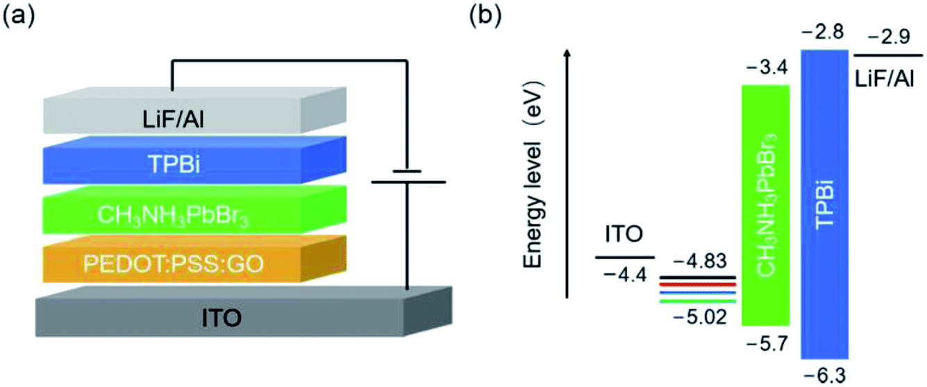 | ||
| Fig. 1 (a) Schematic device structure of PeLEDs using GO doped PEDOT:PSS HTL. (b) Energy levels of individual layers for our PeLEDs. | ||
Fig. 2 shows the ultraviolet photoelectron spectra (UPS) of HTLs. The work function (WF) can be extracted by subtracting secondary electron cutoffs from the excitation energy (21.2 eV).23–25 The secondary electron cutoff of pristine PEDOT:PSS film, PEDOT:PSS:GO film with the GO ratio of 0.1, 0.3 and 0.5 was obtained to be 16.37, 16.28, 16.23, and 16.18 eV, respectively. Thus, the WF of the pure PEDOT:PSS film was calculated to be 4.83 eV, which is well consistent with the previously reported values.23–25 On increasing the GO ratio from 0.1 to 0.5, the WF of the GO-doped film increases from 4.92 eV to 5.02 eV. Therefore, the increased work function of the GO-doped composite film reduces the energy barrier for hole injection between the composite HTL and CH3NH3PbBr3 EML, which can help to elevate the hole injection efficiency.
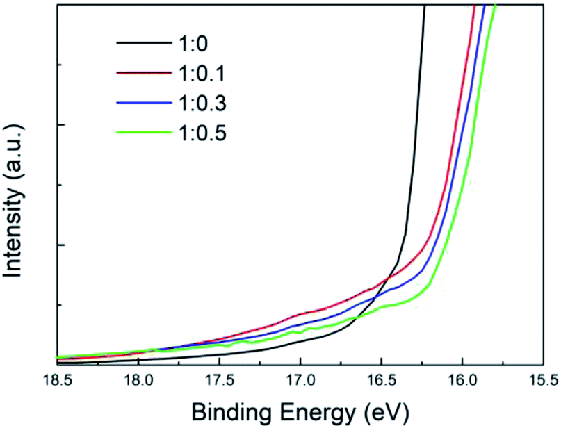 | ||
| Fig. 2 Ultraviolet photoelectron spectra (UPS) of PEDOT:PSS:GO composite films prepared on ITO substrate. | ||
Fig. 3 shows XRD patterns of CH3NH3PbBr3 films spin coated on the PEDOT:PSS films doped with different GO amount. Two typical peaks were found at 15° and 30°, which can be attributed to (100) and (200) crystal planes, respectively.12 In comparison with the reference sample prepared on pure PEDOT:PSS, slightly lower intensities of diffraction peaks were observed for those on all the GO-doped composite films. The diffraction peak intensities of four samples are comparable, suggesting that the GO doping does not affect the structure and crystallinity of perovskite films significantly.
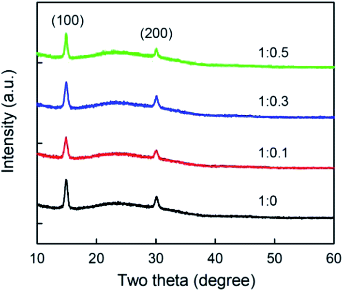 | ||
| Fig. 3 XRD patterns of the CH3NH3PbBr3 films on the PEDOT:PSS films doped with different GO amount. | ||
Fig. 4 presents the SEM images of CH3NH3PbBr3 films spin coated on the PEDOT:PSS films doped with different GO amount. As shown, the surface morphology of the perovskite film is affected by the GO amount in composite HTL. When using the pure PEDOT:PSS, the rough surface of perovskite film is covered by several large flakes. On increasing the GO ratio from 0 to 0.3, the large flakes disappear gradually and small grains form simultaneously. Meanwhile, for the CH3NH3PbBr3 film coated on the PEDOT:PSS:GO (1:0.3) HTL, uniform and compact perovskite films can be obtained. However, when the GO ratio was further increased to 0.5, the perovskite film with poor coverage was found, which may be attributed to the excessive amount of GO. These results indicated that the appropriate amount of GO content can help to obtained the better surface morphology of perovskite films.
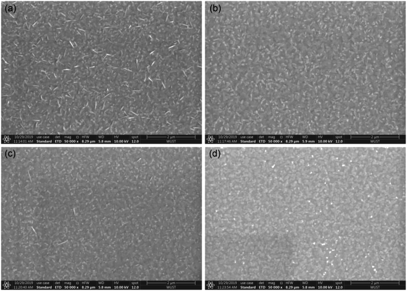 | ||
| Fig. 4 SEM images of the CH3NH3PbBr3 films on the GO-doped composite films with different GO concentration of (a) 1:0, (b) 1:0.1, (c) 1:0.3, (d) 1:0.5. | ||
Fig. 5a presents the steady-state PL spectra of CH3NH3PbBr3 films tested with a 315 nm excitation wavelength. A typical peak at ∼528 nm was found in all the PL spectra. On increasing the GO ratio from 0 to 0.3, the PL peak intensity increases, while the further increased GO leads to the decreased PL intensity. It is indicated that the optimized GO amount is essential for suppressing the quenching of excitons occurred at the interface between HTL and CH3NH3PbBr3 EML, while the overweight GO is not beneficial. On one hand, the increased amount of GO could reduce the contact among PEDOT:PSS and excitons in the EML to some extent, which facilitates the blocking of exciton quenching. Meanwhile, the increased work function of composite HTL reduces the hole injection barrier and prevents the exciton dissociation caused by the large discrepancy of energy levels between PEDOT:PSS and CH3NH3PbBr3, leading to the decreased quenching of excitons at the HTL/EML interface.3,11 Similar results have been reported in polymer LEDs with PEDOT:GO composite HTLs, in which GO reduces the quenching of excitons at HTL/Super Yellow (SY) interface.26 Besides, exciton quenching at the GO/SY interface is found to be much less than that at the PEDOT:PSS/SY interface.27 On the other hand, the excessive GO may induce defect states at the HTL/perovskite EML interface, which leads to the decreased PL intensity. It is found that the trend of the PL peak intensity is in accordance with that of the SEM images. In detail, as the GO ratio increases from 0 to 0.3, the dense and smooth perovskite film indicates the formation of high-quality film, and correspondingly the increased PL strength was obtained. However, when the GO ratio was further increased to 0.5, the decreased PL strength corresponds to the poor-coverage perovskite film.
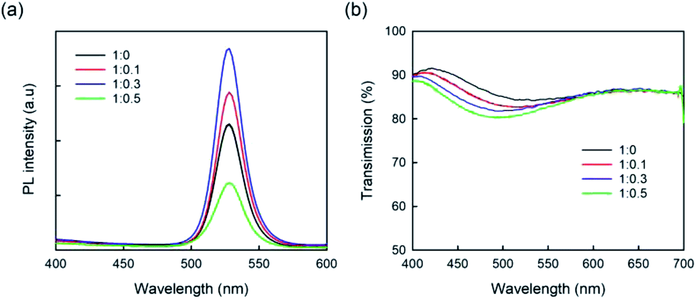 | ||
| Fig. 5 (a) PL and (b) transmittance spectra of the CH3NH3PbBr3 films covered on the PEDOT:PSS films doped with different GO amount. | ||
Fig. 5b shows the wavelength-dependent transmittance of CH3NH3PbBr3 films on the PEDOT:PSS films doped with different GO amount. On increasing the GO ratio from 0 to 0.5, the transmittance near 528 nm decreases slowly. It is noted that the transmittance of the composite film with the largest GO concentration (1:0.5) is still beyond 80% near 528 nm. The comparable values of transmittance were found for four samples, suggesting that the GO doping does not block the light emitting through the HTL region significantly.
Fig. 6a shows the voltage dependence of current density for the PeLEDs with PEDOT:PSS HTLs doped with different GO content, respectively. The turn-on voltage, which is determined with the operating voltage at ∼1 mA cm−2, was lowered from 4.30 V to 3.87 V monotonically with the increased GO ratio from 0 to 0.5. In addition, the current density increases with the increase of the GO amount, suggesting more efficient hole injection. Fig. 6b–d show the luminance, current efficiency (CE), and external quantum efficiency (EQE) of our PeLEDs as functions of current density. The obtained parameters of our PeLEDs are listed in Table 1. For the undoped control PeLED using pure PEDOT:PSS HTL, the maximum values of luminance, CE and EQE are 2305 cd m−2, 1.11 cd A−1 and 0.17%, respectively. On increasing the GO ration to the optimized GO ratio of 0.3, the luminance and CE reach 3302 cd m−2 and 1.92 cd A−1, which increase by 43.3% and 73.0% in comparison with the values of the undoped device, respectively. However, the further increase of GO ratio to 0.5 leads to the decreased efficiency for our device.
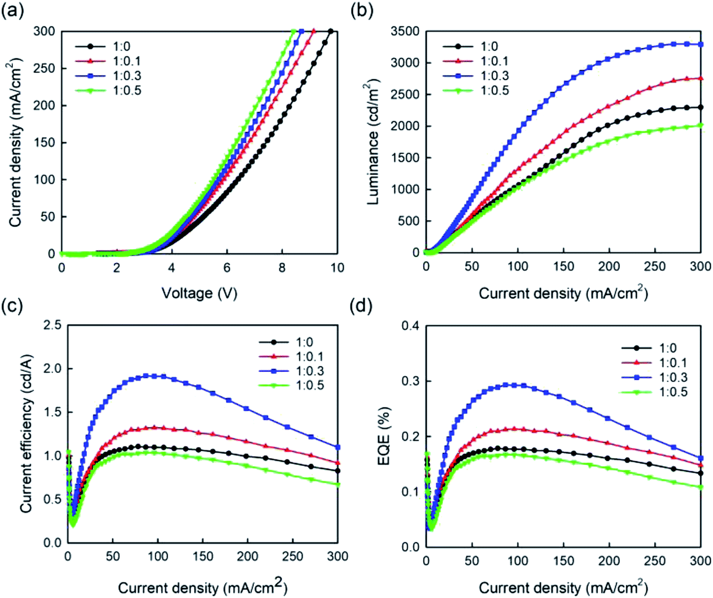 | ||
| Fig. 6 (a) Current density vs. voltage, (b) luminance vs. current density, (c) current efficiency vs. current density, (d) external quantum efficiency vs. current density curves of PeLEDs with PEDOT:PSS HTLs doped with different GO content. | ||
| PEDOT:PSS:GO | Max. luminance (cd m−2) | Max. CE (cd A−1) | Max. EQE (%) | Turn-on voltage (V) |
|---|---|---|---|---|
| 1:0 |
2305 | 1.11 | 0.17 | 4.30 |
| 1:0.1 |
2771 | 1.34 | 0.21 | 4.07 |
| 1:0.3 |
3302 | 1.92 | 0.29 | 3.94 |
| 1:0.5 |
2013 | 1.04 | 0.16 | 3.87 |
In order to determine the role of GO on the hole injection, hole-only devices have also been prepared and tested. Fig. 7 presents the current density of the hole-only devices as a function of voltage, which possess the structure of ITO/HTL/CH3NH3PbBr3/NPB/Al. As shown, after the GO doping in PEDOT:PSS, the current density of the doped sample increases monotonically in comparison with that without GO doping, indicating the enhanced injection ability for holes. It can be caused by the increased WF of HTL and the lower hole injection barrier between composite HTLs and CH3NH3PbBr3 after the GO doping.19 Besides, exciton quenching at the HTL/perovskite interface is another important factor. In LEDs, the external quantum efficiency (EQE) of devices is defined by the ratio between the number of output photons from the device and the number of charges injected to the device. On increasing the GO ratio from 0 to 0.3, the improved efficiency (CE and EQE) of PeLEDs in Fig. 6 can be caused by the combined effects of the enhanced hole injection and reduced exciton quenching evidenced by the PL spectra. The further increase of GO leads to the further enhancement of hole injection shown in Fig. 7. However, the efficiency of PeLED decreases with the excessive GO, which can be mainly explained by the increased exciton quenching shown in PL spectra. Therefore, the increased efficiency of PeLEDs using an optimized PEDOT:PSS:GO as HTL can be caused by the better injection of holes and the suppressed quenching of excitons at the interface between CH3NH3PbBr3 and HTL doped with GO.
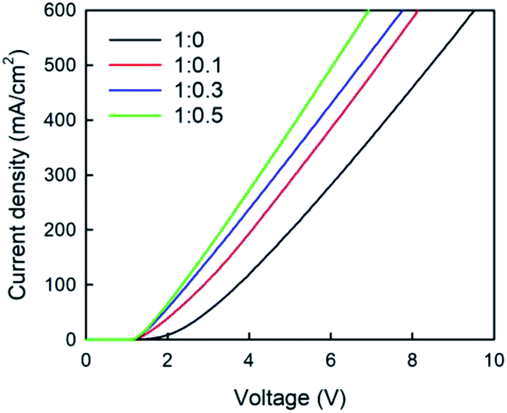 | ||
| Fig. 7 The voltage dependence of current density for the hole-only devices utilizing PEDOT:PSS HTLs doped with different GO amount. | ||
Fig. 8a shows the normalized EL spectra of our PeLEDs, suggesting that all the EL spectra with a peak at ∼528 nm are nearly the same. It is suggested that the GO doping does not change the emission profiles of our devices. Meanwhile, the EL spectra for the PeLED with the optimal PEDOT:PSS:GO (1:0.3) HTL were measured by using different current densities and presented in Fig. 8b. On increasing the current density, the EL peak intensity of the device increases gradually. Meanwhile, the same peak position at ∼528 nm was found in the PeLED at different current densities have, indicating the color stability of PeLEDs.
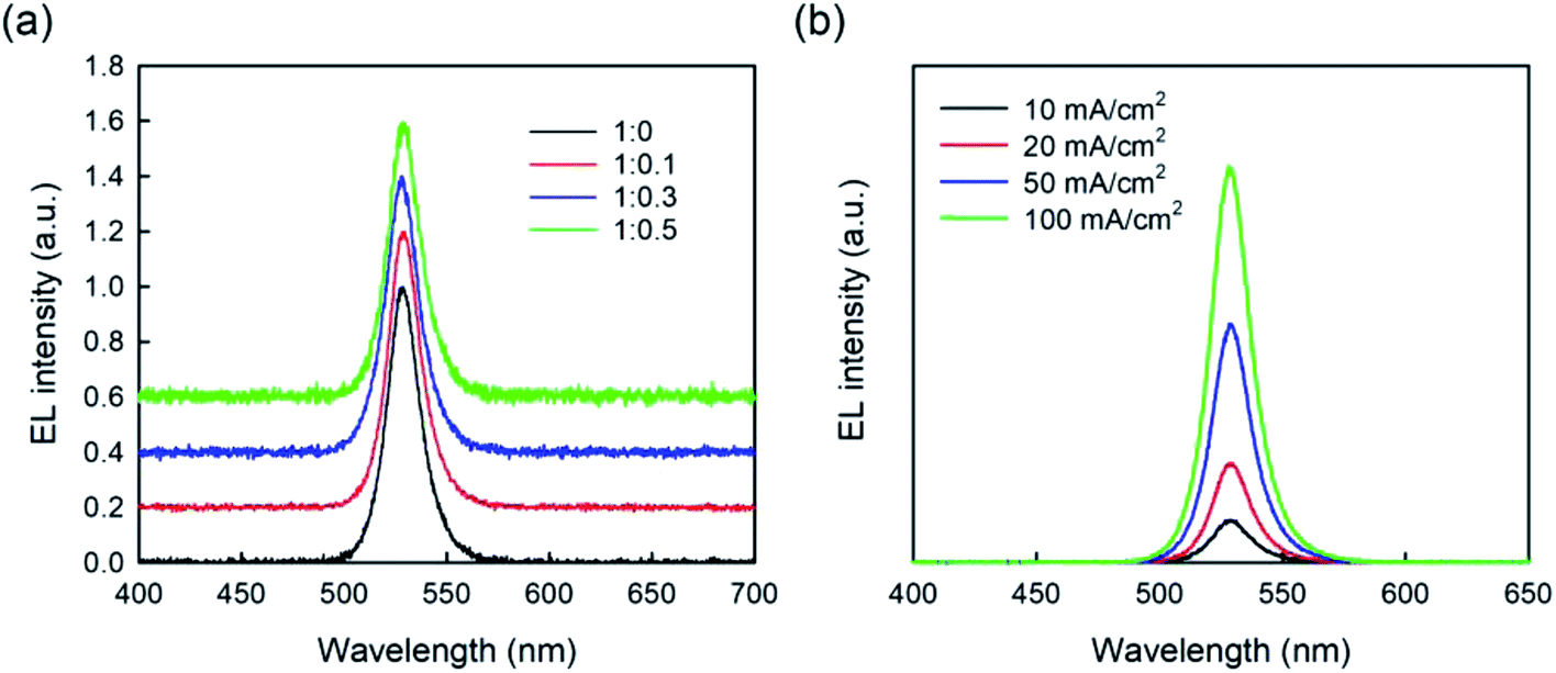 | ||
| Fig. 8 (a) Normalized EL spectra of the PeLEDs with PEDOT:PSS HTLs doped with different GO amount tested at the current density of 50 mA cm−2. (b) EL spectra for the PeLED with the optimal PEDOT:PSS:GO (1:0.3) HTL tested by using different current densities. | ||
4. Conclusions
In conclusion, we reported the enhanced efficiency of PeLEDs by employing GO modified PEDOT:PSS HTLs. On increasing the GO ratio from 0 to 0.5, the increased work function from 4.83 eV to 5.02 eV was found in the composite films, suggesting the increased work function of the composite HTL, which reduces the energy level difference between HTL and perovskite for enhanced hole injection. Meanwhile, the optimized GO amount in PEDOT:PSS can help to reduce the quenching of luminescence occurred at the interface between HTL and CH3NH3PbBr3. On increasing the GO ratio from 0 to 0.3, the maximum value of luminance increases from 2305 cd m−2 to 3302 cd m−2, while the maximum CE increases from 1.11 cd A−1 to 1.92 cd A−1. Further increase of the GO ratio to 0.5 leads to the decrease of luminance and CE. In comparison with the undoped device, the maximum luminance and CE increase by 43.3% and 73.0% in PeLED with an optimized GO ratio (0.3) respectively. The enhanced performance of our PeLEDs can be induced by the better hole injection efficiency and suppressed quenching of excitons at the interface between HTL and CH3NH3PbBr3 EML. These results provide an important approach for designing high-efficiency PeLEDs with 2D materials.Conflicts of interest
There are no conflicts to declare.Acknowledgements
We gratefully acknowledge the financial support from the Foundation of Hubei Provincial Science and Technology Department (Grant No. 2016BKJ005), the Open Foundation of Hubei Key Laboratory for High-efficiency Use of Solar Energy and Operation Control of Energy Storage System (Grant No. HBSEES201705), and the National Natural Science Foundation of China (Grant No. 51602099, 11304092).References
- Z. K. Tan, R. S. Moghaddam, M. L. Lai, P. Docampo, R. Higler, F. Deschler, M. Price, A. Sadhanala, L. M. Pazos, D. Credgington, F. Hanusch, T. Bein, H. J. Snaith and R. H. Friend, Bright light-emitting diodes based on organometal halide perovskite, Nat. Nanotechnol., 2014, 9, 687–692 CrossRef CAS PubMed.
- H. C. Cho, S. H. Jeong, M. H. Park, Y. H. Kim, C. Wolf, C. L. Lee, J. H. Heo, A. Sadhanala, N. Myoung, S. Yoo, S. H. Im, R. H. Friend and T. W. Lee, Overcoming the electroluminescence efficiency limitations of perovskite light-emitting diodes, Science, 2015, 350, 1222–1225 CrossRef CAS PubMed.
- Y. H. Kim, H. Cho, J. H. Heo, T. S. Kim, N. Myoung, C. L. Lee, S. H. Im and T. W. Lee, Multicolored organic/inorganic hybrid perovskite light-emitting diodes, Adv. Mater., 2015, 27, 1248–1254 CrossRef CAS PubMed.
- K. B. Lin, J. Xing, L. N. Quan, F. P. G. de Arquer, X. W. Gong, J. X. Lu, L. Q. Xie, W. J. Zhao, D. Zhang, C. Z. Yan, W. Q. Li, X. Y. Liu, Y. Lu, J. Kirman, E. H. Sargent, Q. H. Xiong and Z. H. Wei, Perovskite light-emitting diodes with external quantum efficiency exceeding 20 per cent, Nature, 2018, 562, 245–248 CrossRef CAS PubMed.
- Y. Cao, N. N. Wang, H. Tian, J. S. Guo, Y. Q. Wei, H. Chen, Y. F. Miao, W. Zou, K. Pan, Y. R. He, H. Cao, Y. Ke, M. M. Xu, Y. Wang, M. Yang, K. Du, Z. W. Fu, D. C. Kong, D. X. Dai, Y. Z. Jin, G. Q. Li, H. Li, Q. M. Peng, J. P. Wang and W. Huang, Perovskite light-emitting diodes based on spontaneously formed submicrometre-scale structures, Nature, 2018, 562, 249–253 CrossRef CAS PubMed.
- L. Liu, S. Li, Y. M. Zhou, L. Y. Liu and X. A. Cao, High-current stressing of organic light-emitting diodes with different electron-transport materials, Microelectron. Reliab., 2017, 71, 106–110 CrossRef CAS.
- W. X. Shi, N. Liu, Y. M. Zhou and X. A. Cao, Effects of postannealing on the characteristics and reliability of polyfluorene organic light-emitting diodes, IEEE Trans. Electron Devices, 2019, 66, 1057–1062 CAS.
- N. Liu, S. J. Mei, D. W. Sun, W. X. Shi, J. H. Feng, Y. M. Zhou, F. Mei, J. X. Xu, Y. Jiang and X. A. Cao, Effects of charge transport materials on blue fluorescent organic light-emitting diodes with a host-dopant system, Micromachines, 2019, 10, 344 CrossRef PubMed.
- X. M. Li and X. A. Cao, Simplified phosphorescent organic light-emitting diodes with a WO3-doped wide bandgap organic charge transport layer, Org. Electron., 2015, 17, 9–14 CrossRef.
- J. S. Kim, R. H. Friend, I. Grizzi and J. H. Burroughes, Spin-cast thin semiconducting polymer interlayer for improving device efficiency of polymer light-emitting diodes, Appl. Phys. Lett., 2005, 87, 023506 CrossRef.
- C. Y. Lin, P. Chen, Z. Y. Xiong, D. B. Liu, G. Wang, Y. Meng and Q. L. Song, Interfacial engineering with ultrathin poly(9,9-di-n-octylfluorenyl-2,7-diyl) (PFO) layer for high efficient perovskite light-emitting diodes, Nanotechnology, 2018, 29, 075203 CrossRef PubMed.
- Y. M. Zhou, S. J. Mei, D. W. Sun, N. Liu, W. X. Shi, J. H. Feng, F. Mei, J. X. Xu, Y. Jiang and X. A. Cao, Improved efficiency of perovskite light-emitting diodes using a three-step spin-coated CH3NH3PbBr3 emitter and a PEDOT:PSS/MoO3-ammonia composite hole transport layer, Micromachines, 2019, 10, 459 CrossRef PubMed.
- D. B. Kim, J. C. Yu, Y. S. Nam, D. W. Kim, E. D. Jung, S. Y. Lee, S. Lee, J. H. Park, A. Y. Lee, B. R. Lee, D. D. Nuzzo, R. H. Friend and M. H. Song, Improved performance of perovskite light-emitting diodes using a PEDOT:PSS and MoO3 composite layer, J. Mater. Chem. C, 2016, 4, 8161–8165 RSC.
- Y. Meng, M. Ahmadi, X. Y. Wu, T. F. Xu, L. Xu, Z. H. Xiong and P. Chen, High performance and stable all-inorganic perovskite light emitting diodes by reducing luminescence quenching at PEDOT:PSS/perovskites interface, Org. Electron., 2019, 64, 47–53 CrossRef CAS.
- Y. M. Zhou, S. J. Mei, D. W. Sun, N. Liu, F. Mei, J. X. Xu and X. A. Cao, Improved charge injection and transport of light-emitting diodes based on two-dimensional materials, Appl. Sci., 2019, 9, 4140 CrossRef CAS.
- W. J. da Silva, A. B. Yusoff and J. Jang, GO:PEDOT:PSS for high-performance green phosphorescent organic light-emitting diode, IEEE Electron Device Lett., 2013, 34, 1566–1568 Search PubMed.
- X. K. Wu, J. Liu, D. Q. Wu, Y. R. Zhao, X. D. Shi, J. Wang, S. J. Huang and G. F. He, Highly conductive and uniform graphene oxide modified PEDOT:PSS electrodes for ITO-free organic light emitting diodes, J. Mater. Chem. C, 2014, 2, 4044–4050 RSC.
- H. S. Dehsari, E. K. Shalamzari, J. N. Gavgani, F. A. Taromi and S. Ghanbary, Efficient preparation of ultralarge graphene oxide using a PEDOT:PSS:GO composite layer as hole transport layer in polymer-based optoelectronic devices, RSC Adv., 2014, 4, 55067–55076 RSC.
- Y. F. Liu, J. Feng, Y. F. Zhang, H. F. Cui, D. Yin, Y. G. Bi, J. F. Song, Q. D. Chen and H. B. Sun, Improved efficiency of indium-tin-oxide-free organic light-emitting devices using PEDOT:PSS/graphene oxide composite anode, Org. Electron., 2015, 26, 81–85 CrossRef CAS.
- J. L. Yang, C. L. Wu, Y. H. Li, W. L. Li, Y. Q. Mia, K. P. Guo, H. H. Liu, H. Wang and Y. A. Wu, Effect of graphene oxide doped PEDOT:PSS as a hole injection layer on the luminescence performance of organic light-emitting diodes, Acta Phys.-Chim. Sin., 2015, 31, 377–383 CAS.
- H. Diker, G. B. Durmaz, H. Bozkurt, F. Yesil and C. Varlikli, Controlling the distribution of oxygen functionalities on GO and utilization of PEDOT:PSS-GO composite as hole injection layer of a solution processed blue OLED, Curr. Appl. Phys., 2017, 17, 565–572 CrossRef.
- J. Chen, J. Y. Pan, Q. Q. Huang, F. Xu, Z. C. Zhang, W. Lei and A. Nathan, Graphene oxide/PEDOT:PSS as injection layer for quantum dot light emitting diode, Phys. Status Solidi A, 2015, 212, 2856–2861 CrossRef CAS.
- C. Zuo and L. Ding, Modified PEDOT Layer Makes a 1.52 V Voc for Perovskite/PCBM Solar Cells, Adv. Energy Mater., 2017, 7, 1601193 CrossRef.
- X. F. Peng, X. Y. Wu, X. X. Ji, J. Ren, Q. Wang, G. Q. Li and X. H. Yang, Modified conducting polymer hole injection layer for high-efficiency perovskite light-emitting devices: enhanced hole injection and reduced luminescence quenching, J. Phys. Chem. Lett., 2017, 8, 4691–4697 CrossRef CAS PubMed.
- Q. Wang, C. C. Chueh, M. Eslamian and A. K.-Y. Jen, Modulation of PEDOT:PSS pH for efficient inverted perovskite solar cells with reduced potential loss and enhanced stability, ACS Appl. Mater. Interfaces, 2016, 8, 32068–32076 CrossRef CAS PubMed.
- J. C. Yu, J. I. Jang, B. R. Lee, G. W. Lee, J. T. Han and M. H. Song, Highly efficient polymer-based optoelectronic devices using PEDOT:PSS and a GO composite layer as a hole transport layer, ACS Appl. Mater. Interfaces, 2014, 6, 2067–2073 CrossRef CAS PubMed.
- B. R. Lee, J. W. Kim, D. Kang, D. W. Lee, S. J. Ko, H. J. Lee, C. L. Lee, J. Y. Kim, H. S. Shin and M. H. Song, Highly efficient polymer light-emitting diodes using graphene oxide as a hole transport layer, ACS Nano, 2012, 6, 2984–2991 CrossRef CAS PubMed.
| This journal is © The Royal Society of Chemistry 2020 |