
 Open Access Article
 This Open Access Article is licensed under a Creative Commons Attribution-Non Commercial 3.0 Unported Licence
One-pot synthesis of MoS2(1−x)Se2x on N-doped reduced graphene oxide: tailoring chemical and structural properties for photoenhanced hydrogen evolution reaction†
Dario
Mosconi
a,
Tomasz
Kosmala
 a,
Marco
Lunardon
a,
Alevtina
Neyman
b,
Maya
Bar-Sadan
b,
Stefano
Agnoli
*a and
Gaetano
Granozzi
a
a,
Marco
Lunardon
a,
Alevtina
Neyman
b,
Maya
Bar-Sadan
b,
Stefano
Agnoli
*a and
Gaetano
Granozzi
a
aDipartimento di Scienze Chimiche, Università di Padova, Via Marzolo 1, 35131 Padova, Italy. E-mail: stefano.agnoli@unipd.it
bDepartment of Chemistry, Ben-Gurion University of the Negev, Beer-Sheva, Israel
First published on 2nd September 2020
Abstract
In this work we designed a one-pot solvothermal synthesis of MoS2(1−x)Se2x nanosheets directly grown on N-doped reduced graphene oxide (hereafter N-rGO). We optimized the synthesis conditions to control the Se![[thin space (1/6-em)]](https://www.rsc.org/images/entities/char_2009.gif) :S ratio, with the aim of tailoring the optoelectronic properties of the resulting nanocomposites for their use as electro- and photoelectro-catalysts in the hydrogen evolution reaction (HER). The synthesis protocol made use of ammonium tetrathiomolybdate (ATM) as MoS2 precursor and dimethyl diselenide (DMDSe) as selenizing agent. By optimizing growth conditions and post-annealing treatments, we produced either partially amorphous or highly crystalline chalcogen-defective electrocatalysts. All samples were tested for the HER in acidic environment, and the best performing among them, for the photoassisted HER. In low crystallinity samples, the introduction of Se is not beneficial for promoting the catalytic activity, and MoS2/N-rGO was the most active electrocatalyst. On the other hand, after the post-annealing treatment and the consequent crystallization of the materials, the best HER performance was obtained for the sample with x = 0.38, which also showed the highest enhancement upon light irradiation.
:S ratio, with the aim of tailoring the optoelectronic properties of the resulting nanocomposites for their use as electro- and photoelectro-catalysts in the hydrogen evolution reaction (HER). The synthesis protocol made use of ammonium tetrathiomolybdate (ATM) as MoS2 precursor and dimethyl diselenide (DMDSe) as selenizing agent. By optimizing growth conditions and post-annealing treatments, we produced either partially amorphous or highly crystalline chalcogen-defective electrocatalysts. All samples were tested for the HER in acidic environment, and the best performing among them, for the photoassisted HER. In low crystallinity samples, the introduction of Se is not beneficial for promoting the catalytic activity, and MoS2/N-rGO was the most active electrocatalyst. On the other hand, after the post-annealing treatment and the consequent crystallization of the materials, the best HER performance was obtained for the sample with x = 0.38, which also showed the highest enhancement upon light irradiation.
Introduction
Molecular hydrogen is considered one of the most promising energy vectors for developing a sustainable energy infrastructure based on the efficient interconversion of chemical energy into electricity and vice versa (usually referred to as hydrogen economy).1,2 Electrolyzers, based on water splitting (WS), are so far the most promising devices to obtain clean hydrogen through the hydrogen evolution reaction (HER) at the cathode side of an electrochemical (EC) cell.3,4 Moreover, a higher sustainability can be obtained if solar energy is exploited to drive the reaction, realizing a photoelectrochemical system (PEC).5–7 This, however, requires the development and optimization of photoelectrocatalysts having tailored optoelectronic properties that allow solar energy harvesting and utilization (i.e. high visible light absorption, slow recombination and fast transport of charge carriers).Although Pt is still the best performing material for HER in terms of both overpotential and current, this metal is a critical raw material, so there are severe problems for its massive exploitation in electrolysers. In addition, Pt alone is not a suitable material for PEC-HER technology since it lacks significant visible light adsorption properties. As an alternative to Pt group metals, many types of earth-abundant transition metals-based catalysts are nowadays intensively investigated: metals, alloys, carbides, nitrides, and, above all, transition metals dichalcogenides (TMDCs). In fact, TMDCs uniquely combine high chemical activity, exhibiting in some case Pt like electronic structure, and outstanding optoelectronic properties such as high visible light adsorption and high mobility of charge carriers, therefore they are undisputedly the most promising candidates for PEC-HER.8–14
In the case of MoS2, most researchers have focused on increasing the number of exposed edges, vacancies or introducing a variety of dopants,15–17 based on the understanding that these are the primary catalytically active sites for HER in acid environment.18 On the other hand, the limited electron conduction of TMDCs can be a problem, as demonstrated by Voiry et al. who reported that the conductivity of the basal plane is a critical factor in the catalytic performance.19 Based on this clue, graphene has been used to support MoS2 to enhance the electrical conductivity with respect to MoS2 alone.20–22 However, while graphene itself can improve the HER performance, being a semimetal, it does not participate directly to PEC processes. Indeed, to enhance the PEC-HER performance of MoS2, usually two main routes are pursued:
• Coupling MoS2 with a suitable material in order to form p–n junctions, which favours the separation of photogenerated charge carriers;22,23
• Tuning the optoelectronic properties of the electrocatalyst to optimize light absorption and band alignment.
The optoelectronic properties of pure TMDCs can be efficiently tailored by creating solid solutions, i.e. forming ternary compounds where the molar fraction either of the metal (i.e. Mo(1−x)WxS2) or of the chalcogenide (i.e. MoS2(1−x)Se2x) is progressively changed.24–32 In these studies, a precise control over the nanosheets composition, shape,24 band gap29 and optical properties30 has been reached, developing materials that have been utilized for the hydrogen production with excellent results.28,31,32 However, synthetic methods, such as Chemical Vapour Deposition (CVD) and heterogeneous solid–gas reactions, which are difficult to scale up, were usually employed. Moreover, harmful gases such as H2Se and H2S were used as precursors or generated as byproduct. On the contrary, wet chemistry routes for synthesizing MoS2(1−x)Se2x have been so far only scarcely investigated.33,34 Therefore, the design of safe and scalable synthetic methods for preparing TMDCs solid solutions could be the key to enable a practical utilization of these materials, overcoming the limitations connected to low throughput and high costs of current preparation methods.
In this work, we developed a one-pot solvothermal synthetic route, alternative to CVD, to produce MoS2(1−x)Se2x with easy-to-tune Se:S ratio. In addition, keeping in mind the final goal of hydrogen production via PEC-HER, we grew the alloy directly on N-doped reduced graphene oxide (N-rGO), to improve both the electrical conductivity and charge separation, thanks to the formation of p–n nanojunctions between MoS2(1−x)Se2x (p-type) and N-rGO (n-type). Since the materials produced by low temperature solvothermal processes are often partially amorphous, we expected for the as-prepared materials a high activity in dark conditions, because of the high abundance of defects, but also a strong recombination tendency during PEC-HER. Hence, we decided to study both the as prepared MoS2(1−x)Se2x/N-rGO and the same samples crystallized at 600 °C in 5% H2 atmosphere. This post-synthetic treatment allows to obtain an ordered structure that enhances the photoactivity, and at the same time leads to the formation of a significant amount of chalcogenide vacancies, improving the HER performance.35–37
Experimental section
Synthesis of MoS2(1−x)Se2x/N-rGO
The syntheses of the starting materials, i.e. N-rGO and ammonium tetrathiomolybdate (ATM) are described in details in the ESI file.† The chemical and morphological characterization of N-rGO is reported in details in the ESI (XPS, Raman and SEM, Fig. S1, S2 and Tables S1, S2†). N-rGO (15 mg) and ATM (33 mg) were mixed in 15 ml of N,N-dimethylformamide (DMF) in a closed glass vial. Different amounts of dimethyldiselenide (DMDSe) (0, 3, 6, 12, 24, 96 μl) were added to the suspension as Se source. The mixture was bath-sonicated for 20 min and then transferred into a Teflon-lined autoclave (23 ml liner). The heat treatment in an electric oven consisted of two steps: 15 h at 180 °C followed by additional 5 h at 200 °C. To remove molecular byproducts, the materials were centrifuged for two times for 8 min at 10000 rpm (23478g) in DMF and ethanol and then dried in vacuum. For comparison, two syntheses with 6 μl of DMDSe were also performed either using a single (15 h at 200 °C) or a two-step step (10 h at 180 °C followed by 5 h at 200 °C) thermal treatment.
To obtain a crystalline product, powders were annealed in a tubular furnace at 600 °C for 1 h (ramp 5 °C min−1) in 95:5 Ar:H2 atmosphere.
To understand the role of ATM in the heterogeneous nucleation and the behaviour of DMDSe at different temperatures, we explored a variety of synthesis protocols with MoCl5 and DMDSe. N-rGO (15 mg) and MoCl5 (34 mg) were poured in a glass vial. 15 ml of DMF and 45 μl of DMDSe were added to the mixture, which was subsequently sonicated for 20 min and transferred into a 23 ml Teflon-lined autoclave. The reaction was carried out for 15 h at 180 °C or with a two-step heating ramp consisting of 15 h at 180 °C and 5 h at 200 °C. After natural cooling down, the materials were cleaned by centrifugation for 8 min at 10000 rpm (23478g) in DMF and in ethanol for two times each, and then dried in vacuum.
Physico-chemical characterization
The surface chemical characterization of the materials has been carried out by XPS using a custom-made UHV system working at a base pressure of 10−10 mbar, equipped with an Omicron EA150 electron analyzer and an Omicron DAR 400 X-ray source with a dual Al–Mg anode. Core level photoemission spectra (Mo 3d, S 2p, Se 3p, Se 3d, C 1s, N 1s and O 1s regions) were collected at rt with a non-monochromatic Mg Kα X-ray source (1253.6 eV) and using an energy step of 0.1 eV, 0.5 s of integration time, and a pass energy of 20 eV. The multipeak analysis of core level photoemission lines was performed by means of Gaussian–Lorentzian functions and subtracting a Shirley background using the KolXPD software.38 The samples were dispersed in 2-propanol and drop casted on an Al support. The nano- and microscale morphology of materials was studied by SEM and TEM. The SEM images were acquired using a field emission source equipped with a GEMINI column (Zeiss Supra VP35), and micrographs were obtained with an acceleration voltage of 5 or 10 kV using in-lens high-resolution detection. The TEM images were acquired using a FEI Tecnai 12 microscope with an acceleration voltage of 100 kV or 120 kV. The Raman spectra were collected using a ThermoFisher DXR Raman microscope using a laser with an excitation wavelength of 532 nm (0.3 mW), focused on the sample with a 50× objective (Olympus). X-Ray Diffraction (XRD) spectra were recorded on a Panalytical Aeris Research instrumentation, using Cu Kα radiation (λ = 0.15406 nm) at 30 kV and 15 mA. The UV-Vis absorption spectroscopy data were acquired using a Varian Cary 50 Spectrophotometer in the 300–800 nm range. In this case, powder samples were dispersed in DMF, forming a stable colloidal dispersion. All spectra were recorded using 1 cm optical path quartz cells. The concentration and the experimental parameters were optimized to minimize scattering effects.Electrochemical characterization
The HER and PEC-HER measurements were carried out in a custom designed three-electrode configuration cell using a Metrohm Autolab PGSTAT-204 (Ecochemie) potentiostat. A glassy carbon (GC) rod used as a counter electrode, whereas an Ag/AgCl(3 M KCl) electrode, calibrated with respect to the reversible hydrogen electrode (RHE), was the reference electrode. All potentials reported in the text and figures are referred to RHE and corrected according to the equation: E(RHE) = E(Ag/AgCl) + 0.225 V + 0.059pH. The EC and PEC experiments were carried out in an Ar-saturated 0.5 M H2SO4 solution prepared from high-purity reagents (Sigma-Aldrich) and ultrapure Milli-Q water with a resistivity of 18.2 MΩ cm. The working electrode was prepared by depositing 12 μl of catalyst ink on a GC electrode (area delimited to 4.5 mm diameter). The catalyst ink consisted of 5 mg of active material, 1.0 ml of N,N-dimethylformamide and 25 μl of Nafion solution. Polarization curves were recorded from +0.2 V to −0.35 V vs. RHE using a scan rate of 0.005 V s−1. All V–t curves were recorded at overpotential (η) equal to 0.18 V. Curves were iR-corrected using the resistance found by EIS. EIS were measured at overpotential of η = 0.18 V and superimposing a small sinusoidal voltage of 10 mV over the frequency range 0.1 MHz to 100 mHz. Charge transfer resistance values were obtained by fitting Nyquist plots using a R(RQ) model circuit. The PEC-HER enhancement was quantified by measuring polarization curves under light illumination from a white LED (WLED) (LDCNW, Metrohm, Autolab LED Driver kit), with a light intensity of 97 mW cm−2. Chopped chronoamperometry curves were acquired by applying a constant cathodic potential (−0.18 V vs. RHE) to the working electrode and the current respond was measured under chopped light from WLED. The same experiments were carried out with different monochromatic LEDs (655 nm, 627 nm, 617 nm, 590 nm, 530 nm, 505 nm and 470 nm) for IPCE analysis. The equation used to calculate IPCE is the following:where h = Planck constant; c = speed of light; e = elementary charge; λ = wavelength (nm); jphoto (λ) = photocurrent density; P(λ) = LED power.

Results and discussion
Optimization and physicochemical characterization of the MoS2(1−x)Se2x/N-rGO hybrids
We aimed at developing an easy and scalable wet chemistry method to prepare advanced MoS2(1−x)Se2x/N-rGO nanohybrids, consisting of p–n nano-junctions between the two moieties, and to investigate the effect of the S/Se ratio and other structural parameters on the PEC-HER performance. To reach these goals, our synthesis protocol was optimized to achieve a high nucleation density of MoS2(1−x)Se2x nanosheets (p-type) on the N-rGO flakes (n-type), since homogeneous nucleation produces MoS2(1−x)Se2x nanoparticles that are only loosely bound to the carbon scaffold. Our synthetic protocol combines two consecutive processes, each activated at a different temperature: the first is the heterogeneous nucleation of MoSx, while the second is its in situ selenization. We chose ATM as MoS2 precursor since, according to the literature, the MoS42− anions decompose at about 180 °C, nucleating MoSx slabs on N-rGO.39 On the other hand, preliminary control experiments have demonstrated that the selenizing agent, DMDSe, becomes effective only at 200 °C. So a tailored two-step heating treatment during the solvothermal process can produce a nanocomposite with rationally designed morphology and stoichiometry: a first step at 180 °C controls the nucleation and growth of MoSx nuclei, whereas during the second step at 200 °C the DMDSe decomposes and produces Se2− ions that exchange for S2− producing the desired sulfoselenides solid solution. Obviously, the duration of each step allows controlling the morphology and stoichiometry of the resulting material. Fig. 1 reports the SEM and TEM micrographs of the MoS2(1−x)Se2x/N-rGO hybrid nanocomposite prepared using 6 μl of DMDSe with different combinations of reaction time and temperature, to study the effect of these parameters on the nucleation density. When the synthesis of MoS2(1−x)Se2x/N-rGO is performed directly at 200 °C, only the homogeneous nucleation of MoS2(1−x)Se2x nanoparticles can be observed, without any nanosheets grown on N-rGO (see Fig. 1A). The material is quite heterogeneous: large aggregates of nanoparticles that are only loosely bound to the N-rGO scaffold can be observed on localized areas. The relatively high temperature produces a massive decomposition of the ATM leading to high supersaturation and the precipitation of MoS2(1−x)Se2x nanoparticles even in the solution bulk.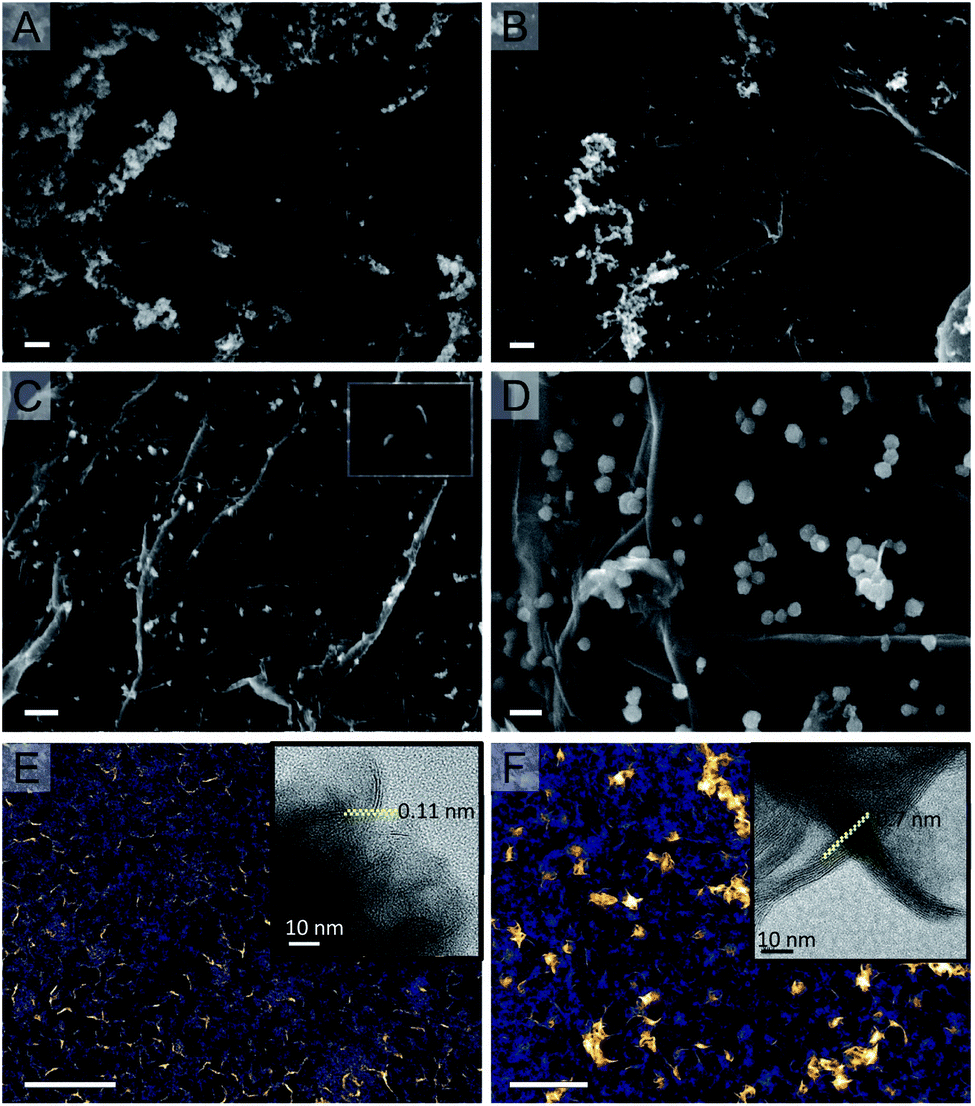 | ||
| Fig. 1 (A–D) SEM images of MoS2(1−x)Se2x/N-rGO prepared using 6 μl of DMDSe: (A) ATM precursor – 15 h at 200 °C without step-temperature heating; (B) ATM – 10 h at 180 °C + 5 h 200 °C; (C) ATM – 15 h at 180 °C + 5 h 200 °C (inset: detail of MoS2(1−x)Se2x slab); (D) MoCl5 as Mo source – 15 h at 180 °C + 5 h 200 °C. (E and F) TEM of the sample shown in panel (C), before (E) and after annealing at 600 °C (F) (scale bar: 200 nm). | ||
On the other hand, when the heating ramp is broke down into a first step at 180 °C followed by second one at 200 °C (Fig. 1B and C), MoS2(1−x)Se2x highly dispersed nanosheets are formed in a quantity that is increasing with the residence time at the lower temperature. Actually, Fig. 1B shows regions where both homogeneous and heterogeneous nucleation have taken place, whereas in Fig. 1C the N-rGO flakes are densely decorated by white features that by TEM analysis resulted to be nanosheets about 2–5 nm thick and with a lateral extension ranging from 20 to 40 nm (mean value 33 nm) (Fig. 1E and F). Therefore, a sufficiently long low-temperature step is necessary to consume most of the ATM and avoid its fast decomposition and consequent uncontrolled precipitation during the following high temperature step.
Higher resolved micrographs, see insets in Fig. 1E, F and S3,† show that the samples before annealing are only partially crystalline and characterized by 2–3 layer stacked nanosheets surrounded by an amorphous matrix. Interestingly the spacing between the crystalline layers is highly expanded, around 1.1 and 1.0 nm, in agreement with XRD measurements (vide infra). Moreover, the following annealing procedure (Fig. 1F) induces a significant crystallization of the amorphous MoS2(1−x)Se2x fraction producing larger nanoplatelets made up by 8–10 layers, and characterized by a diminished interlayer distance (i.e. 0.7–0.8 nm), which is very close to the value expected for bulk MoSe2.
In general, the MoS2(1−x)Se2x nanosheets share a common central spots, which is likely the initial nucleation centre, and diverge from there almost radially, producing a nanoflowers morphology, which is commonly reported in the colloidal or solvothermal synthesis of several TMDCs.40,41 The thickness and extension of the “petals” as well as the voids in between them, increases after the annealing procedure because of the crystallization of amorphous materials, forming larger and better defined “flowers”.
The key role of the heterogeneous nucleation starting from ATM has been also confirmed by performing a control experiment, where MoCl5 and DMDSe where used as Mo and Se sources. The resulting material is shown in Fig. 1D. Polycrystalline nanoparticles with a desert rose-like morphology are homogeneously scattered on the N-rGO support. This special morphology is probably connected to the presence of chloride anions that can be adsorbed on the growing nuclei favouring special crystallographic planes.
Raman spectroscopy and XRD were used to assess the composition and structural features of the hybrid materials as a function of the amount of the DMDSe precursor.30Fig. 2 shows the Raman and XRD spectra of MoS2(1−x)Se2x/N-rGO hybrids prepared with different amount of selenizing agent, before and after the annealing at 600 °C.
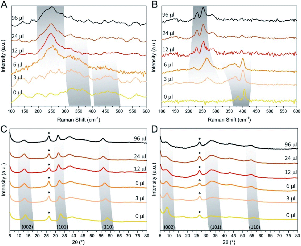 | ||
| Fig. 2 Raman for samples with different Se loading before (A) and after annealing at 600 °C (B). XRD spectra before (C) and after (D) annealing are reported as well. Peaks labelled with diamonds are assigned to the N-rGO support. | ||
The Raman spectra of the as-produced samples show weak and broad peaks, indicating the partially amorphous nature of the MoS2(1−x)Se2x, as often reported in hydro- or solvothermal synthesis of TMDCs.40,42–45 However, some trends can be observed: MoS2/N-rGO (0 μl sample) exhibits two broad bands centred at about 350 and 460 cm−1 (defective form of E12g and A1g normal modes of MoS2).46 Increasing the DMDSe volume, both bands slightly downshift to lower wavenumbers, which is a consequence of the substitution of S with the heavier Se anion. Starting from the 3 μl MoS2(1−x)Se2x sample, another weak mode appears at 260 cm−1 (A1g of MoSe2) that progressively shifts toward lower wavenumbers as the Se amount is increasing. The annealing process induces a crystallization as it can be deduced by Fig. 2B, which exhibits spectra with sharper vibrational bands. Moreover, as in the case of as-prepared samples, we observe a shift of the bands as a function of the content of Se. The Raman spectrum of MoS2/N-rGO shows the typical spectral fingerprint of semiconducting 2H-phase MoS2, with E12g and A1g modes at 383 and 405 cm−1, respectively. The difference between the centroids of these peaks is a useful tool to estimate the average number of layers in MoS2 particles and, according to the literature, the measured 22 cm−1 frequency separation indicates about 3 layers per stack, which is compatible with the TEM images.47,48 In the case of the annealed samples by increasing the Se content, we can observe a typical “two mode behaviour”, which does not entail phase separation, but it is consistent with the formation of a solid solution.49–51 The two-mode behaviour occurs when the frequencies of phonon modes in the pure compounds (e.g. MoS2 and MoSe2) differ sufficiently from one another. The phonon features of pure MoS2 and MoSe2 are separated of about 200 cm−1, which allows for the observation of the two-mode behaviour in MoS2(1−x)Se2x/N-rGO hybrid. The consequence is that E12g and A1g vibrations of MoS2 tends to downshift as S is exchanged for Se, with a concomitant broadening of E12g. Similarly, MoSe2-like features start appearing at 270 cm−1 in the 3 μl sample and shifts down to 253 cm−1 in the 96 μl sample, at the same time getting narrower. It is worth mentioning that above 12 μl few changes can be observed in Raman analysis, moreover the typical Raman spectrum of MoSe2 (single sharp peak at 238 cm−1, see Fig. S3B†) was not observed. This may be due to an equilibrium between Sx− and Sex− species in the closed solvothermal environment, which does not allow reaching the full anion exchange and obtaining pure MoSe2/N-rGO. The XRD spectra are in excellent agreement with the trend observed in Raman spectroscopy data.
All the peaks highlighted in Fig. 2C and D, downshift with the Se content, indicating the expansion of the TMDC lattice due to the larger size of Se anions with respect to S anions. Moreover, the 2θ values and peak shape tend to stabilize above 12 μl of DMDSe, getting close to, but not reaching, the distinctive fingerprint observed in the single phase MoSe2/N-rGO sample (Fig. S5A and B†). Comparing the features of as-prepared and annealed samples, significant changes can be observed: the more ordered structure obtained after annealing results in sharper diffraction features, and the (002) peak undergoes an average shift of 4.8°. Being this peak related to the interlayer distance, such shift reveals a contraction from 10.1 Å to 6.5 Å of the MoS2(1−x)Se2x crystal structure during the annealing. In the literature, it has been already demonstrated that higher interlayer distance can be beneficial for HER performance, therefore as-prepared samples are expected to outperform the crystalline analogues in dark conditions.52,53
These considerations were further confirmed by an extensive XPS study. First of all, XPS was used to evaluate the chemical composition of the resulting MoS2(1−x)Se2x solid solutions. In Table 1 we report a comparison between the nominal stoichiometry based on the molar ratio of S and Se in the reaction environment and that deduced by the intensity of the photoemission spectra using a multipeak analysis of S 2p–Se 3p region. A detailed description of this procedure is fully reported in the ESI.† As it can be seen from the reported values, at low DMDSe concentration, there is a strong uptake of Se in the solid solution, whereas at higher concentration the introduction of selenium becomes more and more difficult. Finally, it is worth mentioning that annealing at 600 °C in hydrogen (95:5 Ar:H2) produced a systematic chalcogenide removal of about 15% (see Tables S3 and S4†). Indeed, as-prepared samples are slightly overstoichiometric, with an average (S + Se)/Mo ratio of 2.1. On the other hand, after the thermal treatment, the (S + Se)/Mo ratio decreased to an average value of 1.75, which is consistent with the value observed by Li et al. in similar conditions,35 who demonstrated that S vacancies are helpful to catalyse the HER and that H2 stripping can be exploited to obtain very defective structures with S/Mo close to 0.1. However, to the best of authors' knowledge, this treatment was never applied on MoS2(1−x)Se2x. Interestingly, our XPS data indicated that the hydrogen treatment does not lead to relevant changes in the Se/S ratio, since both elements are reduced only by 10–20%, independently on the composition of the pristine solid solutions. Mo 3d core levels are shown in Fig. 3A (as-prepared) and Fig. 3B (crystalline): in both cases a clear shift to lower binding energy (BE) of Mo 3d5/2 peak is observed by increasing the amount of Se precursor. Considering the crystalline samples, the Mo 3d line of MoS2/N-rGO (0 μl) has the expected position of the semiconducting 2H-phase of MoS2 (228.9 eV);54–57 increasing the quantity of Se causes the BE to shift continuously toward lower values. The value observed for the 96 μl sample was 228.6 eV (0.3 eV lower than 0 μl) and, even if close, it is not the same BE (228.5 eV) observed for commercial MoSe2 and MoSe2/N-rGO obtained from the experiment with MoCl5 (see Fig. S19A†). This is an additional indication that using the combination of ATM and DMDSe is not possible to reach full anion exchange, at least within the tested conditions. The deconvolution of Mo 3d region always shows the presence of a main component related to MoS2(1−x)Se2x, a minor component at 232.1 eV ascribed to MoOx due to surface oxidation, and finally a component downshifted of 0.8 eV with respect to the main component, which is ascribed to undercoordinated molybdenum atoms, surrounding chalcogenide vacancies. Moreover, the evolution of the S 2s (226.0 eV) and Se 3s (229.1 eV) spectra is consistent with the progressive introduction of Se in the MoS2 lattice.
| μl DMDSe | x value in MoS2(1−x)Se2x | Chemical structuresc | |||
|---|---|---|---|---|---|
| Nominala | XPSb amorp. | XPSb cryst. | As-prepared | Crystalline | |
| a Calculated from the ratio of total Se and total S present in the precursors. b Determined by multipeak analysis of S 2p/Se 3p region. c Deduced from XPS measured x values and (S + Se)/Mo ratios. | |||||
| 0 | 0 | 0 | 0 | MoS2.10 | MoS1.80 |
| 3 | 0.11 | 0.23 | 0.24 | MoS1.62Se0.48 | MoS1.29Se0.41 |
| 6 | 0.20 | 0.37 | 0.38 | MoS1.32Se0.78 | MoS1.12Se0.68 |
| 12 | 0.33 | 0.58 | 0.58 | MoS0.84Se1.16 | MoS0.76Se1.04 |
| 24 | 0.50 | 0.62 | 0.65 | MoS0.82Se1.38 | MoS0.63Se1.17 |
| 96 | 0.80 | 0.75 | 0.72 | MoS0.53Se1.58 | MoS0.48Se1.22 |
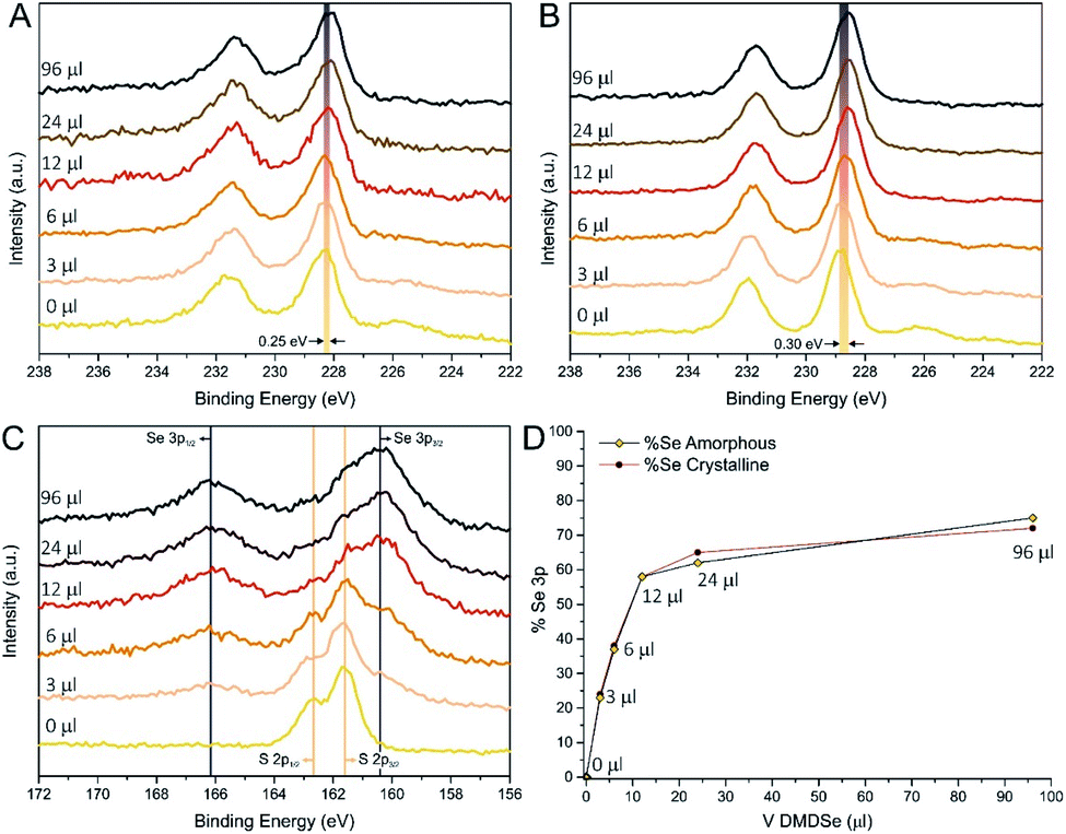 | ||
| Fig. 3 XPS spectra of Mo 3d core levels for as-prepared (A) and crystalline (B) MoS2(1−x)Se2x/N-rGO samples. Evolution of S 2p and Se 3p regions of crystalline samples (C), with related Se content calculated by multipeak analysis (D). | ||
Additionally, in the case of as-prepared samples, the XPS analysis confirms the hypothesis suggested by Raman spectroscopy, since the Mo 3d photoemission lines of as-prepared MoS2(1−x)Se2x/N-rGO show broader peaks with respect to the annealed counterpart, with an average 24% broadening of Full Width at Half Maximum (FWHM) of the Mo 3d5/2 peak. Furthermore, an average BE downshift of 0.5 eV was found comparing as-prepared and annealed samples, which is a typical behaviour of amorphous materials.46
HER and PEC-HER characterization
Both as-prepared and annealed materials were tested for HER in typical acid medium (0.5 M H2SO4) in dark conditions and under illumination. In principle, we expected that the partially amorphous samples were more active than crystalline analogues in dark conditions because of the expanded interlayer distance and of the higher defectivity that should provide a higher number of active sites. On the other hand, the more ordered structure and lack of recombination centres in annealed samples should be beneficial for PEC-HER and guarantee a better stability. Moreover, the formation of p–n junctions between p-type MoS2(1−x)Se2x and n-type N-rGO should favour charge separation enhancing the PEC performance. Finally the efficiency of visible light absorption must be critically dependent on the composition since the MoS2(1−x)Se2x bandgap can be tuned by adjusting the Se:S ratio.22,29,30,58
Linear Sweeps Voltammetries (LSVs) in dark conditions revealed remarkable performances for most of the as prepared samples (Fig. 4). Surprisingly, the best performance was found for the MoS2/N-rGO (0 μl) sample: it needed an overpotential of only 0.16 V to drive 10 mA cm−2 current density (η10). The introduction of a low amount of Se (3 and 6 μl) (Table 2 as-prepared materials, underwent a large performance drop after the thermal treatment: the η10 value is almost doubled in the case of MoS2 and for the mixed samples with the lowest Se content. According to literature data, pure MoSe2 has better or equal onset potential with respect to a MoS2 sample with the same morphology and number of active sites, thanks to the improved electrical properties.59–61 Clearly, after crystallization, the MoS2 structure was re-established, lowering the number of active sites, as proven by the change in η10. The outstanding Tafel slope of 39 mV dec−1 clearly does not stem only from the typical edge-site of MoS2, but most probably from the coexistence of other lattice defects, such as residual S22− groups that are known to have low energy barriers for H2 formation62 (incidentally, in the S 2p core level of the 0 μl sample, it can be observed a high BE component that can be ascribed to these species, see Fig. S6B†). Analogous defects in amorphous MoSe2 are much less active in the HER, as also proved by the modest performances reported in the literature.63
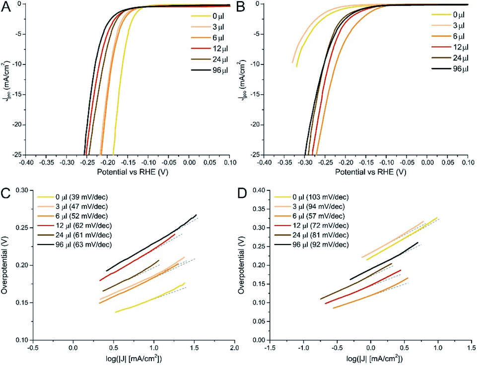 | ||
| Fig. 4 Linear sweeps voltammetries for as-prepared (A) and crystalline (B) MoS2(1−x)Se2x/N-rGO samples. The related Tafel plots are reported for as-prepared (C) and crystalline (D) samples. | ||
| V DMDSe (μl) | XPS composition (Se:S) |
Overpotential at 10 mA cm−2 (V) | Tafel slope (mV dec−1) | Exchange current density j0 (μA cm−2) | ||||
|---|---|---|---|---|---|---|---|---|
| As-prepared | Crystalline | As-prepared | Crystalline | As-prepared | Crystalline | As-prepared | Crystalline | |
| 0 | 0:100 |
0:100 |
0.16 | 0.32 | 39 | 103 | 4.47 | 7.94 |
| 3 | 23:77 |
24:76 |
0.19 | 0.33 | 47 | 94 | 2.34 | 8.51 |
| 6 | 37:63 |
38:62 |
0.19 | 0.21 | 52 | 57 | 2.45 | 15.8 |
| 12 | 58:42 |
58:42 |
0.22 | 0.24 | 62 | 72 | 1.91 | 12.6 |
| 24 | 62:38 |
65:35 |
0.21 | 0.25 | 61 | 81 | 2.09 | 10.7 |
| 96 | 75:25 |
72:28 |
0.23 | 0.25 | 63 | 92 | 1.51 | 11.0 |
As mentioned above, all samples underwent similar changes upon annealing, which are the crystallization of TMDC structure and the formation S/Se vacancies due to H2 stripping (see Table S4†). Due to the presence of S vacancies, the Tafel slope is slightly lower than typical literature values,35 indicating that the Volmer step (i.e. reductive adsorption of H species from H3O+) is the bottle neck of the reaction. In the 3 μl sample, despite the presence of 24% of Se, the structure is still very similar to MoS2, as proven by Raman spectroscopy and by XPS. The latter, in particular, indicates that this amount of Se is not sufficient to induce a strong modification in the electronic structure, as demonstrated by the small BE shift (ca. 0.1 eV) in the Mo 3d region. Therefore, only a slight improvement in the activity (Tafel slope from 103 to 94 mV dec−1) is determined by the introduction of this amount of Se. On the contrary, the 6 μl sample (about 38% Se) has an intermediate structure and maintains an excellent performance even after annealing, increasing the η10 of only 0.02 V. This is further validated by the analysis of the Tafel slope, which remains almost unchanged even after annealing. So, even if the structure crystallizes (as confirmed by the changes of Raman, XRD and XPS spectra), this solid solution outperforms materials with a composition close to the pure phases. In the literature such behaviour has been rationalized by density functional calculations28,64 suggesting that in several mixed anions dichalcogenides the hydrogen adsorption energy is reduced with respect to pure phases because of either the variation of structural parameters or electronic effect connected to the shift of the d band centroid. In our case our XPS data seems to suggest that electronic effect should be minimal, on the contrary structural parameters such as a progressive strain the anion lattice as a function of the Se/S ratio should be more relevant as evidenced by Raman spectroscopy and XRD. When the amount of Se is further increased in the range 40–70%, the solid solutions can preserve the electroactivity after the thermal treatments, even if the overall performance is slightly worse compared to the 6 μl sample. Moreover, the progressive worsening of the Tafel slope for increasing Se percentage demonstrates that the optimal Se amount is around 40%. Surprisingly, j0 increased for all samples after annealing, but reaching a maximum in the case of 6 μl, which exhibited an exchange current value of 15.8 μA cm−2. Rct tendency underwent the same changes of η10, showing a massive improvement for the 0 and 3 μl samples and a lower increase for samples with a Se content higher than 38%. Finally, crystallization was beneficial for stability, since for annealed materials the chronopotentiometric test (Fig. S22†) showed only a small 3% increase of the overpotential needed to generate the reference current.
When comparing with other published data of MoS2(1−x)Se2x prepared via wet chemistry routes, similar performances were found.33,65 For example, Gong et al. designed an hot injection protocol for unsupported MoS2(1−x)Se2x and they found that mixed chalcogenides material (in particular sample with x = 0.5) exhibited performances better than pure phases, with Se:S ratios similar to those found by us. In addition, similar overpotentials (η10 of 0.17 V) and Tafel slopes (48 mV dec−1) were measured in their materials. Analogous figures of merit (η10 of 0.17 V and Tafel slopes 43.3 mV dec−1) were also found for MoSe2 and MoS2 thin films supported on gold nanorods.66 Considering graphene–TMDCs hybrids,23,43 if pure MoS2 or MoSe2 were used as active material, generally worse HER activity were recorded, with η10 above 0.25 V. However, in other cases MoS2(1−x)Se2x-based materials exhibited even better performances, recording η10 even lower than 0.1 V, but in all the cases CVD protocols were required to achieve sulphidization or selenization or special types of current collectors such as nickel foams were used.28,31,32,67
HER performed under illumination with white LED (WLED, Fig. 5A and B) confirmed the hypothesis presented above: as-prepared samples show a very small improvement at 10 mA cm−2, especially for MoS2 and high Se-loaded samples. The highest improvement was found on the 6 μl sample, with a gain on η10 of about 5%. On the other hand, the improvement on the η10 value in crystalline samples was found to be double, reaching 12% in the case of the 6 μl sample. The Tafel slope stayed the same in dark and under illumination in all the measured samples. Moreover, we acquired chronoamperometric measurements with chopped WLED light of the 6 μl MoS2(1−x)Se2x/N-rGO sample: as it is possible to see in Fig. 5C, the as-prepared material exhibits a slow and weak response to light, even if a 0.3 mA cm−2 enhancement was found when light was turned on. On the other hand, after annealing the material showed a sharper response when and in this case the improvement was about 1 mA cm−2, corresponding to a 20% current density gain upon irradiation.
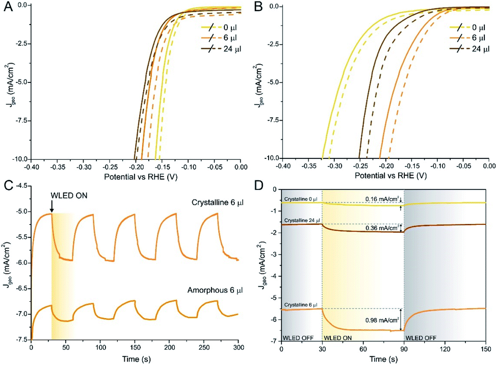 | ||
| Fig. 5 Polarization curves in dark (solid line) and under illumination (dashed line) for several as-prepared (A) and annealed (B) MoS2(1−x)Se2x/N-rGO samples. In panel (C) the J–t curve (η = 0.18 V) comparing the light response of 6 μl MoS2(1−x)Se2x/N-rGO before and after annealing. (D) J–t curves for 0, 6 and 24 μl crystalline MoS2(1−x)Se2x/N-rGO recorded at η = 0.18 V using WLED as light source. | ||
Mott–Schottky analysis (Fig. S23†) and EIS measurements (Fig. S24†) were performed on the crystalline samples. Mott–Schottky plots allow to determine the conductivity type of the semiconductor at the working electrode, having the plot a positive (negative) slope when the analysed material is n-type (p-type). Obviously, when Mott–Schottky analysis is carried out on a multi-component material, the contribution of all the semiconducting constituents will be traced in the plot. Hence, in the case of p–n junctions both p- and n-type contributions have to be observed, resulting in a V-shaped plot.
This kind of plot was found in all the analysed materials and, considering the literature reference, we can attribute the positive slope contribution to N-rGO and the other to MoS2(1−x)Se2x.22,23,27 In all the tested materials, we observed a progressive downshift of the V position with the increase of the Se content. We can assume that this shift is related to the change in electronic structure due to the formation of the solid solution.
Consequently, the flat band potential (Vfb) shifted in the same way, proving directly that our synthesis protocol allows tuning the band-gap of the supported TMDC material.
On the other hand, EIS experiments are useful to observe the evolution of the charge transfer resistance (Rct) as a function of the experimental conditions. We decided to perform EIS at the same overpotential (η = 0.18 V) in dark and under WLED illumination, in order to crosscheck both the performances in dark and the enhancement under illumination. Table 3 summarizes the values obtained by fitting the spectra showed in Fig. S24.†
| V DMDSe (μl) | R ct (Ω) dark | R ct (Ω) WLED | Relative Rct variation |
|---|---|---|---|
| 0 μl | 443 | 301 | 32% |
| 6 μl | 56 | 29 | 48% |
| 24 μl | 135 | 82 | 39% |
As mentioned above, Rct values measured for experiments in dark followed the same trend observed both in HER activity and kinetics. The introduction of 38% of Se (6 μl sample) induced an 8-fold reduction of Rct with respect to pure MoS2, confirming the improvement in the reaction rate. However, the further increase in Se content produced a double value of Rct, so the 24 μl sample showed only average activity, as already observed in Tafel analysis. As expected, all the materials showed a reduction of Rct upon WLED illumination, since the photo-induced promotion of electrons in MoS2(1−x)Se2x conduction band produces in all the cases a higher number of carriers ready to be transferred to the electrolyte. Moreover, the presence of p–n junctions helps to stabilize photo-generated excitons suppressing recombination. However, different efficiencies are expected, as already observed in photocurrents and gain in η10: again the 6 μl sample exhibited the best photo-enhancement, halving the resistance under illumination. In the 0 and 24 μl MoS2(1−x)Se2x/N-rGO, samples the trend was still the same: a 39% decrease of Rct value was observed in the high Se-loaded sample, that is mid-way between the 6 μl sample and pure MoS2/N-rGO (32% reduction).
In order to shed some light on the influence of Se:S ratio on the photoinduced reaction, we also recorded UV-Vis spectra of all the crystalline materials to check absorption bands position. As before, we analysed the 0, 6 and 24 μl samples. UV-Vis spectroscopy (Fig. 6A) shows the typical electronic transitions of Mo-based TMDCs, that are three excitonic features named as A, B and C, respectively. The A and B excitonic peaks stem from direct transitions from two filled bands, which are split due to spin–orbit coupling, to the conduction band minimum at the K point, the indirect transition between the valence band maximum located at the Γ point and the conduction band minimum located at the point is responsible for the C feature.68–70 As it can be seen in Fig. 6A, the A and B peaks underwent a 70 nm (0.2 eV) redshift with increasing the Se amount, which is consistent with the band gap narrowing due to the change in the solid solution composition.30,71–73 On the contrary, the C-exciton peak remained rather constant (ca. 475 nm, 2.6 eV) among the samples, even if a broadening of the band could be observed.
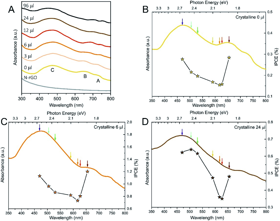 | ||
| Fig. 6 (A) UV-Vis spectra of crystalline MoS2(1−x)Se2x/N-rGO crystalline samples. (B–D) IPCE measurements recorded at η = 180 mV for 0 μl (B), 6 μl (C) and 24 μl (D) samples. In the plots, both the ICPE values (right axis) and the absorbance spectrum (left axis) of the sample are shown. | ||
In Fig. 6B–D, IPCE measurements are reported for several materials using seven different monochromatic LEDs in the visible range (see the wavelengths in the Experimental section).
All the MoS2(1−x)Se2x/N-rGO hybrids showed similar trends, according to the corresponding absorption spectra. All the samples exhibited higher photo-activity when irradiated with wavelengths that match the main electronic transitions, in particular the B exciton in the low energy range of the spectrum. Above the B transition, a substantial photoactivity drop was observed because of the lack of optical transitions around 620 nm, being the absorbance in this region of UV-Vis spectra mainly due to scattering events. When the photon energy is increased, the IPCE slowly rises following the absorption profile and peaking in correspondence of the C band maximum. At this wavelength, the IPCE reaches values close to those measured in the deep-red range, despite the indirect nature of the C transition. Only for the 24 μl sample, higher ICPE values were recorded in the blue region, however, at high Se content, the A and B exciton peaks are beyond the available LEDs, so we are measuring the decaying tail observed in the previous materials. Therefore, we suppose that the Se-containing samples would be even more active if irradiated with near-infrared light in the region of A and B excitons, widening the wavelength range that can be utilized for enhancing HER. Moreover, we can qualitatively observe that the increment in the IPCE with photon energy is steeper at larger Se content, which can be associated with the broadening of C exciton band highlighted by UV-Vis spectra.
Considering the values of IPCE, 6 μl MoS2(1−x)Se2x/N-rGO outperformed the other materials, with values ranging between 0.8% and 1.2%, with an average 4- and 2-fold increment with respect to 0 and 24 μl samples, respectively. These values are rather low compared to others reported in the literature,74–76 but it has to be considered that no bulk semiconductor was used as support for the electroactive material and, consequently, all the light absorption is carried out only by the MoS2(1−x)Se2x nanosheets on the electrode. Indeed, when similar systems are considered (i.e. active material supported on photoinactive electrodes), our materials are at the state of the art.77,78
Conclusions
In this work, we designed a novel solvothermal synthesis for the preparation of molybdenum sulfoselenides on a N-rGO scaffold, with the goal of forming p–n nanojunctions to exploit PEC-HER. The utilization of ATM and DMDSe as reactants allowed obtaining the desired morphology and to vary the fraction x in the 0–0.75 range, without the direct use of harmful gases like H2S and H2Se. However, because the resulting materials were partially amorphous, an annealing step was necessary to induce the MoS2(1−x)Se2x crystallization. The structure and the composition were thoroughly analysed by mean of XRD, Raman and XPS, which were used to follow the evolution of composition-dependent parameters.Both as-prepared and annealed materials were tested in HER conditions (0.5 M H2SO4) in dark and under illumination. The experiments confirmed the expectations: as-prepared samples, given their partially amorphous nature, were more active than crystalline analogues in dark conditions because of the expanded interlayer distance and the higher defectivity that provide a larger number of active sites, however they exhibited limited stability in working conditions. On the other hand, the more ordered structure of the crystalline samples leads to materials with improved durability and with better performances in photoassisted experiments. Among as-prepared samples, pure MoS2/N-rGO was the best performing material, with a progressive worsening of activity with the increase of Se, proving that the active sites of amorphous MoS2 have better catalytic performances compared to selenide counterparts. On the contrary, annealed Se-containing samples exhibited better HER activity and kinetics, with the material prepared from 6 μl of DMDSe (about 38% of Se) outperforming the others. Under illumination, each material showed a different response, revealing that introducing 38% of Se boosted the photo-enhancement as well. Overall the body of our experimental data indicate that the functional properties of solid solutions of TMDCs are strongly dependent on the composition and require a careful optimization in order to achieve improved performances. We showed that the structural properties of the anion lattice (presence of vacancies, Se/S ratio, anion disorder) impact strongly the electrochemical activity as well as photoactivity. In the case of crystalline samples, given the small changes observed in XPS and optical absorption spectra, the chemical activity is likely connected to the presence of local defects and strain in the solid solution, while electronic effect are likely less relevant. Interestingly, the photoactivity is highest in the same compositional range when electroactivity reaches its maximum and the charge transfer resistance is lowest. This seems to suggest that the photo-HER activity is limited by the chemical properties and specifically by catalytic activity and not by the material ability to harvest light and transport charge carriers. This is therefore the critical factor that has to be optimized in material design.
Considering the lack of potentially scalable synthesis of MoS2(1−x)Se2x in the literature, we think that this work can pave the way toward the further improvement of supported solid solutions of TMDCs, with the goal of obtaining better performances and stronger photo-enhancement while taking into consideration the production safety (e.g. no harmful gases) and scalability.
Conflicts of interest
There are no conflicts to declare.Acknowledgements
This work was partially supported by the following projects: Financial support from the Italian MIUR (PRIN 2015: SMARTNESS, 2015K7FZLH; PRIN2017: Multi-e, 20179337R7), and MAECI Italy-China bilateral project (GINSENG, PGR00953). Cariparo Foundation is acknowledged for funding (project Synergy, Progetti di Eccellenza 2018).Notes and references
- I. Staffell, D. Scamman, A. Velazquez Abad, P. Balcombe, P. E. Dodds, P. Ekins, N. Shah and K. R. Ward, Energy Environ. Sci., 2019, 12, 463–491 RSC.
- J. O. Abe, A. P. I. Popoola, E. Ajenifuja and O. M. Popoola, Int. J. Hydrogen Energy, 2019, 44, 15072–15086 CrossRef CAS.
- M. David, C. Ocampo-Martínez and R. Sánchez-Peña, J. Energy Storage, 2019, 23, 392–403 CrossRef.
- Z. Yan, J. L. Hitt, J. A. Turner and T. E. Mallouk, Proc. Natl. Acad. Sci. U. S. A., 2019, 2019, 201821686 Search PubMed.
- C. A. Arancibia-Bulnes, I. Arauzo, C. E. Arreola-Ramos, G. Barone, M. Bayat, A. A. Bayod-Rújula, G. Buffo, A. Buonomano, A. K. Cuentas-Gallegos, M. A. Farkhondehfal, D. Ferrero, R. Figaj, C. Forzano, H. Guzmán, S. Hernández, S. Karellas, M. Kayfeci, A. Keçebaş, K. R. Krishnamurthy, A. Lanzini, P. Marocco, A. Martinez-Gracia, H. Nair, H. Narayanan, B. Nastasi, A. Palombo, H. Romero-Paredes, T. C. Roumpedakis, N. Russo, M. Santarelli, K. R. Tolod, G. Torzillo, E. Touloupakis, J. Uche, P. J. Valades-Pelayo, L. Vanoli, H. I. Villafán-Vidales and B. Viswanathan, Solar Hydrogen Production, Elsevier Inc, 2019 Search PubMed.
- S. Yun, N. Vlachopoulos, A. Qurashi, S. Ahmad and A. Hagfeldt, Chem. Soc. Rev., 2019, 48, 3705–3722 RSC.
- D. M. Robinson, Y. B. Go, M. Mui, G. Gardner, Z. Zhang, D. Mastrogiovanni, E. Garfunkel, J. Li, M. Greenblatt and G. C. Dismukes, J. Am. Chem. Soc., 2013, 135, 3494–3501 CrossRef CAS.
- L. Nie and Q. Zhang, Inorg. Chem. Front., 2017, 4, 1953–1962 RSC.
- C. Wu, J. Zhang, X. Tong, P. Yu, J. Y. Xu, J. Wu, Z. M. Wang, J. Lou and Y. L. Chueh, Small, 2019, 15, 1–25 Search PubMed.
- T. Yao, X. An, H. Han, J. Q. Chen and C. Li, Adv. Energy Mater., 2018, 8, 1–36 Search PubMed.
- B. Peng, P. K. Ang and K. P. Loh, Nano Today, 2015, 10, 128–137 CrossRef CAS.
- Q. Ding, B. Song, P. Xu and S. Jin, Chem, 2016, 1, 699–726 CAS.
- H. Zhong, C. A. Campos-Roldán, Y. Zhao, S. Zhang, Y. Feng and N. Alonso-Vante, Catalysts, 2018, 8, 559 CrossRef.
- A. Ennaoui, S. Fiechter, C. Pettenkofer, N. Alonso-Vante, K. Büker, M. Bronold, C. Höpfner and H. Tributsch, Sol. Energy Mater. Sol. Cells, 1993, 29, 289–370 CrossRef CAS.
- D. Mosconi, P. Till, L. Calvillo, T. Kosmala, D. Garoli, D. Debellis, A. Martucci, S. Agnoli and G. Granozzi, Surfaces, 2019, 2, 531–545 CrossRef.
- A. E. Russell, M. S. Faber, S. Jin, H. Zhang, Q. Yun, Q. Lu, X. Zhang, C. Tan, X. Geng, W. Sun, W. Wu, B. Chen, A. Al-Hilo, M. Benamara, H. Zhu, F. Watanabe, J. Cui, T. Chen, X. Chia, A. Y. S. Eng, A. Ambrosi, S. M. Tan, M. Pumera, D. Genuit, P. Afanasiev, M. Vrinat, M.-R. Gao, M. K. Y. Chan, Y. Sun, K. S. Subrahmanyam, D. Sarma, C. D. Malliakas, K. Polychronopoulou, B. J. Riley, D. A. Pierce, J. Chun, M. G. Kanatzidis, J. D. Benck, T. R. Hellstern, J. Kibsgaard, P. Chakthranont, T. F. Jaramillo, M. A. Worsley, S. J. Shin, M. D. Merrill, J. Lenhardt, A. J. Nelson, L. Y. Woo, A. E. Gash, T. F. Baumann, C. A. Orme, K. Chang, X. Hai, H. Pang, H. Zhang, L. Shi, G. Liu, H. Liu, G. Zhao, M. Li, J. Ye, E. Ahn, B.-S. Kim, L. Liao, J. Zhu, X. Bian, L. Zhu, M. D. Scanlon, H. H. Girault, B. Liu, B. Balasubramanian, A. L. Ortiz, S. Kayatakoglu and D. P. Harris, Nat. Commun., 2015, 9, 5326–5333 Search PubMed.
- J. Zhang, T. Wang, P. Liu, S. Liu, R. Dong, X. Zhuang, M. Chen and X. Feng, Energy Environ. Sci., 2016, 9, 2789–2793 RSC.
- T. F. Jaramillo, K. P. Jorgensen, J. Bonde, J. H. Nielsen, S. Horch and I. Chorkendorff, Science, 2007, 317, 100–102 CrossRef CAS.
- D. Voiry, M. Salehi, R. Silva, T. Fujita, M. Chen, T. Asefa, V. B. Shenoy, G. Eda and M. Chhowalla, Nano Lett., 2013, 13, 6222–6227 CrossRef CAS.
- Y. Li, H. Wang, L. Xie, Y. Liang, G. Hong and H. Dai, J. Am. Chem. Soc., 2011, 133, 7296–7299 CrossRef CAS.
- X. Zheng, J. Xu, K. Yan, H. Wang, Z. Wang and S. Yang, Chem. Mater., 2014, 26, 2344–2353 CrossRef CAS.
- F. Carraro, L. Calvillo, M. Mattia Cattelan, M. Favaro, M. Righetto, S. Silvia Nappini, I. Igor Píš, V. Celorrio, D. J. Fermín, A. Martucci, S. Agnoli and G. Granozzi, ACS Appl. Mater. Interfaces, 2015, 7, 25685–25692 CrossRef CAS.
- F. Meng, J. Li, S. K. Cushing, M. Zhi and N. Wu, J. Am. Chem. Soc., 2013, 135, 10286–10289 CrossRef CAS.
- Q. Feng, N. Mao, J. Wu, H. Xu, C. Wang, J. Zhang and L. Xie, ACS Nano, 2015, 9, 7450–7455 CrossRef CAS.
- W. Zhang, X. Li, T. Jiang, J. Song, Y. Lin, L. Zhu and X. Xu, Nanoscale, 2015, 7, 13554–13560 RSC.
- M. Zheng, J. Du, B. Hou and C.-L. Xu, ACS Appl. Mater. Interfaces, 2017, 9, 26066–26076 CrossRef CAS.
- T. Kosmala, H. Coy Diaz, H. P. Komsa, Y. Ma, A. V. Krasheninnikov, M. Batzill and S. Agnoli, Adv. Energy Mater., 2018, 8, 1–8 Search PubMed.
- H. Zhou, F. Yu, Y. Huang, J. Sun, Z. Zhu, R. J. Nielsen, R. He, J. Bao, W. A. Goddard III, S. Chen and Z. Ren, Nat. Commun., 2016, 7, 12765 CrossRef CAS.
- S. H. Su, Y. Te Hsu, Y. H. Chang, M. H. Chiu, C. L. Hsu, W. T. Hsu, W. H. Chang, J. H. He and L. J. Li, Small, 2014, 10, 2589–2594 CrossRef CAS.
- J. Mann, Q. Ma, P. M. Odenthal, M. Isarraraz, D. Le, E. Preciado, D. Barroso, K. Yamaguchi, G. Von Son Palacio, A. Nguyen, T. Tran, M. Wurch, A. Nguyen, V. Klee, S. Bobek, D. Sun, T. F. Heinz, T. S. Rahman, R. Kawakami and L. Bartels, Adv. Mater., 2014, 26, 1399–1404 CrossRef CAS.
- H. Yang, T. Zhang, H. Zhu, M. Zhang, W. W. Wu and M. L. Du, Int. J. Hydrogen Energy, 2017, 42, 1912–1918 CrossRef CAS.
- S. Hussain, K. Akbar, D. Vikraman, K. Karuppasamy, H.-S. Kim, S.-H. Chun and J. Jung, Inorg. Chem. Front., 2017, 2068–2074 RSC.
- Q. Gong, L. Cheng, C. Liu, M. Zhang, Q. Feng, H. Ye, M. Zeng, L. Xie, Z. Liu and Y. Li, ACS Catal., 2015, 5, 2213–2219 CrossRef CAS.
- G. Cai, L. Peng, S. Ye, Y. Huang, G. Wang and X. Zhang, J. Mater. Chem. A, 2019, 7, 9837–9843 RSC.
- L. Li, Z. Qin, L. Ries, S. Hong, T. Michel, J. Yang, C. Salameh, M. Bechelany, P. Miele, D. Kaplan, M. Chhowalla and D. Voiry, ACS Nano, 2019, 13, 6824–6834 CrossRef CAS.
- X. Wang, Y. Zhang, H. Si, Q. Zhang, J. Wu, L. Gao, X. Wei, Y. Sun, Q. Liao, Z. Zhang, K. Ammarah, L. Gu, Z. Kang and Y. Zhang, J. Am. Chem. Soc., 2020, 142, 4298–4308 CrossRef CAS.
- Y. Yin, J. Han, Y. Zhang, X. Zhang, P. Xu, Q. Yuan, L. Samad, X. Wang, Y. Wang, Z. Zhang, P. Zhang, X. Cao, B. Song and S. Jin, J. Am. Chem. Soc., 2016, 138, 7965–7972 CrossRef CAS.
- KolXPD homepage, https://www.kolibrik.net/kolxpd/ Search PubMed.
- T. P. Prasad, E. Diemann and A. Müller, J. Inorg. Nucl. Chem., 1973, 35, 1895–1904 CrossRef CAS.
- C. Dai, E. Qing, Y. Li, Z. Zhou, C. Yang, X. Tian and Y. Wang, Nanoscale, 2015, 7, 19970–19976 RSC.
- O. E. Meiron, L. Houben and M. Bar-Sadan, RSC Adv., 2015, 5, 88108–88114 RSC.
- D. Yang, M. Tayebi, Y. Huang, H. Yang and Y. Ai, Sensors, 2016, 16, 1911 CrossRef.
- S. Xu, Z. Lei and P. Wu, J. Mater. Chem. A, 2015, 3, 16337–16347 RSC.
- Y. Jia, H. Wan, L. Chen, H. Zhou and J. Chen, Mater. Lett., 2017, 195, 147–150 CrossRef CAS.
- X. T. Tran, S. Poorahong and M. Siaj, RSC Adv., 2017, 7, 52345–52351 RSC.
- T. Kosmala, D. Mosconi, G. Giallongo, G. A. Rizzi and G. Granozzi, ACS Sustainable Chem. Eng., 2018, 6, 7818–7825 CrossRef CAS.
- H. Li, Q. Zhang, C. C. R. Yap, B. K. Tay, T. H. T. Edwin, A. Olivier and D. Baillargeat, Adv. Funct. Mater., 2012, 22, 1385–1390 CrossRef CAS.
- C. Lee, H. Yan, L. E. Brus, T. F. Heinz, J. Hone and S. Ryu, ACS Nano, 2010, 4, 2695–2700 CrossRef CAS.
- W. H. Weber and R. E. Merlin, Raman Scattering in Materials Science, 2000 Search PubMed.
- S. Pagliara, L. Sangaletti, L. E. Depero, V. Capozzi and G. Perna, Solid State Commun., 2000, 116, 115–119 CrossRef CAS.
- Y. Liang, L. Zhai, X. Zhao and D. Xu, J. Phys. Chem. B, 2005, 109, 7120–7123 CrossRef CAS.
- M.-R. Gao, M. K. Y. Chan and Y. Sun, Nat. Commun., 2015, 6, 7493 CrossRef.
- M. Jiang, J. Zhang, M. Wu, W. Jian, H. Xue, T. W. Ng, C. S. Lee and J. Xu, J. Mater. Chem. A, 2016, 4, 14949–14953 RSC.
- J. C. Muijsers, T. Weber, R. M. Vanhardeveld, H. W. Zandbergen and J. W. Niemantsverdriet, J. Catal., 1995, 157, 698–705 CrossRef CAS.
- G. Tuci, D. Mosconi, A. Rossin, L. Luconi, S. Agnoli, M. Righetto, C. Pham-Huu, H. Ba, S. Cicchi, G. Granozzi and G. Giambastiani, Chem. Mater., 2018, 30, 8257–8269 CrossRef CAS.
- D. Garoli, D. Mosconi, E. Miele, N. Maccaferri, M. Ardini, G. Giovannini, M. Di Palo, S. Agnoli and F. De Angelis, Nanoscale, 2018, 10, 17105–17111 RSC.
- D. Mosconi, G. Giovannini, A. Jacassi, P. Ponzellini, N. Maccaferri, P. Vavassori, M. Serri, M. Dipalo, D. Darvill, F. De Angelis, S. Agnoli and D. Garoli, ACS Omega, 2019, 4, 9294–9300 CrossRef CAS.
- C. H. Lee, S. Lee, G. S. Kang, Y. K. Lee, G. G. Park, D. C. Lee and H. I. Joh, Appl. Catal., B, 2019, 258, 117995 CrossRef CAS.
- D. Escalera-López, Z. Lou and N. V. Rees, Adv. Energy Mater., 2019, 9, 1802614 CrossRef.
- A. Eftekhari, Appl. Mater. Today, 2017, 8, 1–17 CrossRef.
- J. D. Wiensch, J. John, J. M. Velazquez, D. A. Torelli, A. P. Pieterick, M. T. McDowell, K. Sun, X. Zhao, B. S. Brunschwig and N. S. Lewis, ACS Energy Lett., 2017, 2234–2238 CrossRef CAS.
- X. Dai, K. Du, Z. Li, M. Liu, Y. Ma, H. Sun, X. Zhang and Y. Yang, ACS Appl. Mater. Interfaces, 2015, 7, 27242–27253 CrossRef CAS.
- Q. T. Nguyen, P. D. Nguyen, D. Nguyen, Q. D. Truong, T. T. Kim Chi, T. T. D. Ung, I. Honma, N. Q. Liem and P. D. Tran, ACS Appl. Mater. Interfaces, 2018, 10, 8659–8665 CrossRef CAS.
- Y. Zhou, Y. Wang, H. Zhao, J. Su, H. Zhang and Y. Wang, J. Catal., 2020, 381, 84–95 CrossRef CAS.
- R. Bar-Ziv, O. E. Meiron and M. Bar-Sadan, Nanoscale, 2018, 10, 16211–16216 RSC.
- Z. Liu, X. Zhang, Y. Gong, Q. Lu, Z. Zhang, H. Cheng, Q. Ma, J. Chen, M. Zhao, B. Chen, Y. Chen, X. J. Wu, P. Yin, L. Gu, Y. Du and H. Zhang, Nano Res., 2019, 12, 1301–1305 CrossRef CAS.
- L. Yang, W. Wang, Q. Fu, J. Zhang and B. Xiang, Electrochim. Acta, 2015, 185, 236–241 CrossRef CAS.
- K. F. Mak, C. Lee, J. Hone, J. Shan and T. F. Heinz, Phys. Rev. Lett., 2010, 105, 2–5 CrossRef.
- G. Pagona, C. Bittencourt, R. Arenal and N. Tagmatarchis, Chem. Commun., 2015, 51, 12950–12953 RSC.
- G. Y. Jia, Y. Liu, J. Y. Gong, D. Y. Lei, D. L. Wang and Z. X. Huang, J. Mater. Chem. C, 2016, 4, 8822–8828 RSC.
- A. Ramasubramaniam, Phys. Rev. B: Condens. Matter Mater. Phys., 2012, 86, 1–6 CrossRef.
- L. Yang, X. Wu, X. Zhu, C. He, M. Meng, Z. Gan and P. K. Chu, Appl. Surf. Sci., 2015, 341, 149–156 CrossRef CAS.
- M. Velický and P. S. Toth, Appl. Mater. Today, 2017, 8, 68–103 CrossRef.
- L. Zhang, C. Liu, A. B. Wong, J. Resasco and P. Yang, Nano Res., 2014, 8, 281–287 CrossRef.
- X. Zong, H. Yan, G. Wu, G. Ma, F. Wen, L. Wang and C. Li, J. Am. Chem. Soc., 2008, 130, 7176–7177 CrossRef CAS.
- K. C. Kwon, S. Choi, K. Hong, C. W. Moon, Y. S. Shim, D. H. Kim, T. Kim, W. Sohn, J. M. Jeon, C. H. Lee, K. T. Nam, S. Han, S. Y. Kim and H. W. Jang, Energy Environ. Sci., 2016, 9, 2240–2248 RSC.
- F. M. Pesci, M. S. Sokolikova, C. Grotta, P. C. Sherrell, F. Reale, K. Sharda, N. Ni, P. Palczynski and C. Mattevi, ACS Catal., 2017, 4990–4998 CrossRef CAS.
- J. Xiao, Y. Zhang, H. Chen, N. Xu and S. Deng, Nano-Micro Lett., 2018, 10, 60 CrossRef.
Footnote |
| † Electronic supplementary information (ESI) available: Detailed synthesis (GO, N-rGO, ATM); GO and N-rGO structural characterization; control MoSe2/N-rGO characterization; extended XPS characterization of MoS2(1−x)Se2x/N-rGO; extended electrochemical characterization of MoS2(1−x)Se2x/N-rGO. See DOI: 10.1039/d0na00375a |
| This journal is © The Royal Society of Chemistry 2020 |