
 Open Access Article
 This Open Access Article is licensed under a Creative Commons Attribution-Non Commercial 3.0 Unported Licence
Light extraction from quantum dot light emitting diodes by multiscale nanostructures†
Shujie
Wang
,
Chenran
Li
,
Yang
Xiang
,
Hui
Qi
,
Yan
Fang
,
Aqiang
Wang
,
Huaibin
Shen
 and
Zuliang
Du
*
and
Zuliang
Du
*
Key Laboratory for Special Functional Materials of Ministry of Education, National & Local Joint Engineering Research Centre for High-efficiency Display and Lighting Technology, School of Materials and Engineering, Collaborative Innovation Centre of Nano Functional Materials and Applications, Henan University, Kaifeng 475004, China. E-mail: zld@henu.edu.cn
First published on 25th March 2020
Abstract
Improving the light extraction efficiency by introducing optical–functional structures outside of quantum dot light emitting diodes (QLEDs) for further enhancing the external quantum efficiency (EQE) is essential for their application in display and lighting industries. Although the efficiency of QLEDs has been optimized by controlling the synthesis of the quantum dots, the low outcoupling efficiency is indeed unresolved because of total internal reflections, waveguides and metal surface absorptions within the device. Here, we utilize multiscale nanostructures attached to the outer surface of the glass substrate to extract the trapped light from the emitting layers of QLEDs. The result indicates that both the EQE and luminance are improved from 12.29% to 17.94% and 122![[thin space (1/6-em)]](https://www.rsc.org/images/entities/char_2009.gif) 400 cd m−2 to 178700 cd m−2, respectively. The maximum EQE and current efficiency improve to 21.3% and 88.3 cd A−1, respectively, which are the best performances among reported green QLEDs with light outcoupling nanostructures. The improved performance is ascribed to the elimination of total internal reflection by multiscale nanostructures attached to the outer surface of the QLEDs. Additionally, the simulation results of the finite-difference time domain (FDTD) also demonstrate that the light trapping effect is reduced by the multiscale nanostructures. The design of novel light outcoupling nanostructures for further improving the efficiency of QLEDs can promote their application in display and lighting industries.
400 cd m−2 to 178700 cd m−2, respectively. The maximum EQE and current efficiency improve to 21.3% and 88.3 cd A−1, respectively, which are the best performances among reported green QLEDs with light outcoupling nanostructures. The improved performance is ascribed to the elimination of total internal reflection by multiscale nanostructures attached to the outer surface of the QLEDs. Additionally, the simulation results of the finite-difference time domain (FDTD) also demonstrate that the light trapping effect is reduced by the multiscale nanostructures. The design of novel light outcoupling nanostructures for further improving the efficiency of QLEDs can promote their application in display and lighting industries.
Introduction
Due to their unique fluorescence properties, including narrow full width at half-maximum (FWHM), easier color tuning without changing the composition, high photoluminescence (PL) quantum yield (QY), and the solution processability of colloidal quantum dots (QDs), quantum dot light emitting diodes (QLEDs) have been considered as one of the competitors for organic light emitting diodes (OLEDs) in the future of the display industry.1–3 In particular, recent advances suggest that QLEDs with both high brightness and high external quantum efficiency (EQE) are potential candidates for lighting further increasing their application areas.4,5 To date, the record efficiencies of QLEDs are indeed lower than those of the more investigated OLEDs. This is particularly true for the three primary colored QLEDs; the best-reported external quantum efficiency (EQE) of red, green and blue QLEDs is limited to about 20%.5–7 The technical challenge of QLED devices is that their EQE is limited by the light outcoupling efficiency of the device, which is indeed unresolved because of total internal reflection, waveguide (WG) and metal surface absorption (SPP).8,9Numerous studies have reported that the light extractions of OLEDs and QLEDs could be enhanced through introduction of internal or external light-extraction layers.10–14 For example, we have demonstrated that introducing internal PEDOT:PSS grating nanostructures can effectively extract the waveguided light from QLEDs by nanoimprint lithography techniques.15 However, the extraction of the trapped light to WG and SPP modes is more challenging since the insertion of internal structures inside the QLEDs always changes the morphology of the quantum dot emitting layers and then deteriorates the performance of the device. In particular, the functional layers of QLEDs are prepared by an all solution method, while OLEDs are prepared by an evaporation method. The patterned optical structure often affects the morphology of the QD emitting layers and then decreases the efficiency of the devices.16 Instead of internal structures, constructing light outcoupling structures directly outside the device without affecting the electrical properties of the device is beneficial for the large-scale preparation and industrial application for QLEDs.17 Nevertheless, the commonly reported nanostructures limit the further development of high-performance QLEDs due to their inherent drawbacks such as incomplete reflection suppression, high haze, angular dependence, and image blurring.18,19 When comparing the performance of QLEDs and OLEDs, the most significant difference is that QLEDs have symmetric and Gaussian-like emission spectra with a full width half maximum (FWHM) typically as narrow as 30 nm, while for OLEDs the spectrum is usually broader (∼100 nm) and more asymmetric.20 The narrower emission spectra of QLEDs require more delicately designed nanostructures to further improve the EQE and match the performance of OLEDs. Thus new light outcoupling structure design is needed for improving the low extraction efficiency of QLEDs. Traditionally, the vast variety of approaches for light outcoupling structures can be categorized as periodic features but which typically introduce an undesired angular dependency of the emission spectrum. The disordered structures do not have selectivity to wavelength, which can enhance the light emission intensity in all directions, but its light output efficiency is low.21 Therefore, it is challenging and meaningful to construct multiscale nanostructures for light extraction from QLEDs which combines the advantages of periodic and disordered nanostructures.
In this paper, multiscale nanostructures are delicately designed through nanoimprint combined with reactive ion beam etching (RIE) techniques. Highly effective extraction of total internal reflection light from the emitting layer of QLEDs is carried out by attaching grid/wrinkle patterns outside the glass substrate without changing the electrical properties of the device. Both the EQE and luminance for green QLEDs improved from 12.29% to 17.94%, and 122400 cd m−2 to 178700 cd m−2, respectively. The maximum EQE and current efficiency of 21.3% and 88.3 cd A−1, respectively have been achieved which are the best values ever reported for light outcoupling QLEDs, to the best of our knowledge. The observed improvement is ascribed to the elimination of total internal reflection by finite-difference time domain (FDTD) simulation methods.
Experimental details
The fabrication process of multiscale nanostructures is schematically illustrated in Fig. 1. Initially, the Si substrate with grating structures is used as a master mold with a line width of 350 nm, gap of 350 nm, and height of 130 nm. Here the Intermediate Polymer Stamp (IPS) is used to replicate patterned nanostructures of the Si master mold and then act as stamp in the nanoimprint process. By rotating the grating Si mold 90° after first imprinting with 20 bar for 30 s at 150 °C and imprinting twice with lower temperatures and higher pressure (30 bar for 30 s at 135 °C), two dimensional grid patterns of IPS are obtained as shown in Fig. 1(c) and (d). In order to protect the grating structure of the first impression, the initial temperature of the second imprint should be smaller than that of the first impression.22 The poly(dimethylsiloxane) (PDMS) is prepared by mixing a basic agent and firming agent with a 10:1 weight ratio. By curing at 80 °C for 1 h under vacuum conditions, the air bubbles are extracted and the grid feature of the master mold is replicated on the PDMS. The wrinkle structure is fabricated and tailored by RIE treatments. In our experiment, the etching is performed with etching times of 5 s, 10 s, 30 s and 60 s on a patterned PDMS substrate. The multiscale nanostructures are obtained as shown in Fig. 1(g)–(j).
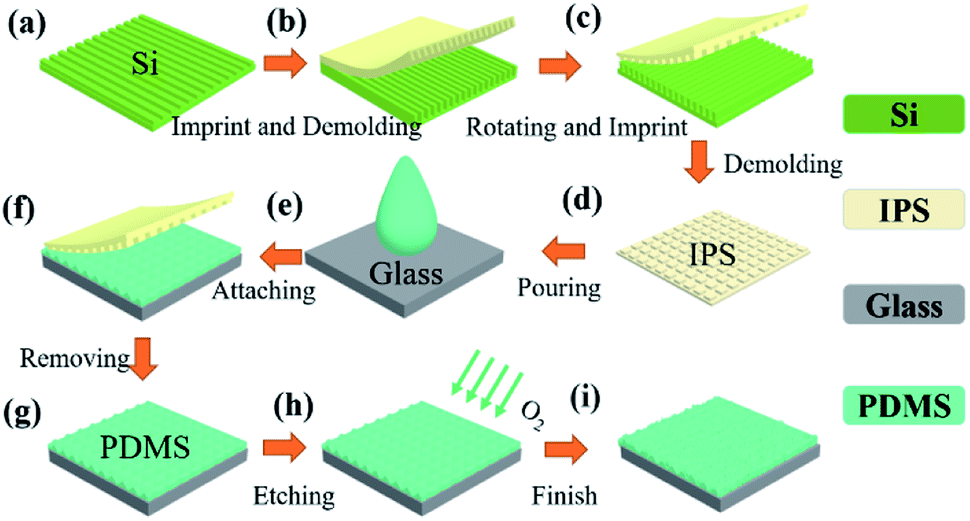 | ||
| Fig. 1 Schematic fabrication process of grid/wrinkle nanostructures. | ||
The synthesis of core–shell CdSe@ZnS/ZnS QDs is carried out according to the literature.23 The detailed preparation process can be referred to in our previous work.15 The TEM images and absorption spectrum of the QDs are shown in Fig. S1.† For device fabrication, the QD emitting layers of core–shell CdSe@ZnS/ZnS are dispersed in n-octane (18 mg mL−1). A patterned indium tin oxide (ITO) glass substrate is used as the anode, washed in an ultrasonic bath of detergent, de-ionized water, acetone, and IPA for 15 minutes in sequence followed by an ultraviolet ozone treatment for 15 minutes. PEDOT:PSS is used as a hole injection layer (HIL) spin-coated on the ITO substrates at 4000 rpm and then thermally annealed at 130 °C for 15 min. Poly[9,9-dioctyl-fluorene-co-N-(4-butylphenyl)-diphenylamine] (TFB) is used as hole transport layer (HTL) dissolved in chlorobenzene with a concentration of 8 mg mL−1 followed by a bake-out at 150 °C for 30 min. After that, ZnO nanoparticles used as an electron transport layer (ETL) are spin-coated at 2000 rpm from a 30 mg mL−1 ethanol solution, followed by thermal treatment at 60 °C for 30 min. Finally, the multilayer samples are loaded into a high-vacuum deposition chamber to thermally deposit the cathode, aluminum (Al), in which a shade mask was used to define the top Al contact and form an active device area of 0.04 cm2. The patterned PDMS films were attached on the ITO substrates for the light outcoupling of the QLED devices.
The absorption and photoluminescence (PL) of the QD solutions were measured by using a UV-vis spectrometer (Lambda 950, PerkinElmer, USA) and a spectrofluorometer (JY HORIBA FluoroLog-3), respectively. The TEM image of the QDs was obtained on a JEM-2010 microscope. Field emission-SEM (Nova Nano SEM 450) and AFM (Dimension Icon) were used to analysis the morphological properties of the samples. The electrical characteristics of the fabricated devices just as current density–voltage–luminance (J–V–L) and EL spectra were measured by using a Photo Research Spectra Scan PR-735 spectrometer equipped with a Keithley 2400 voltmeter.
Results and discussion
Fig. 2(a)–(d) show the atomic force microscopy (AFM) images of PDMS films with grid and wrinkle nanostructures. From the AFM image analysis, the line width of the grid patterns is about 350 nm with a period of 350 nm which indicated that IPS stamps with full feature sizes are successfully transferred in a low cost manner. The hot imprint process here makes the PDMS expand which in turn affects the height of the grid structures lower than the mold itself. The height of grid PDMS is about 70 nm which is lower than that of the IPS stamps (90 nm). Periodic wrinkles of the PDMS films are prepared by RIE methods.24 During the RIE process, the organic moieties on the surface of PDMS can be oxidized to volatile substances just as H2O and CO2 by the reactive atomic oxygen. The residue of silica will form a thin layer behaving as wrinkles on the surface of the PDMS films. Through controlling the exposure time, the period and size of the wrinkles can be elaborately controlled.25 As shown in Fig. 2(b)–(d), when the etching time is 10 s, 30 s and 60 s, the height of the wrinkles varies from 35 nm to 65 nm and 110 nm. At the same time, the period of the wrinkles is also decreased. Fig. 3(a) and (b) show the AFM images of multiscale grid/wrinkle nanostructures of PDMS films fabricated by nanoimprint combined with RIE techniques. The result indicates that the morphology of the grid structure is well preserved without changing the period and linewidth. It is obvious that the wrinkle structures on the surface of the gird are successfully achieved through the SEM images shown in Fig. S2†. We should note that there is a hollow-core structure formed at the intersection of the PDMS films which is caused by the elastomer of the PDMS film. During the RIE process, the internal stress of PDMS will cause a depression in the middle area of the intersection. As the etching time increases from 30 s to 60 s, the height of the multiscale nanostructures increases from 90 nm to 110 nm, and the height of the hollow-core structures is further increased, while the periodicity of the whole structure is maintained.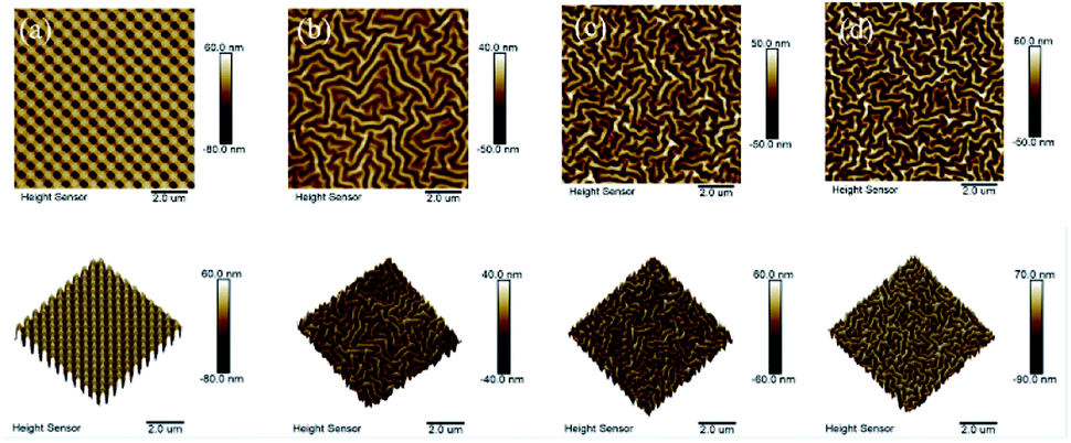 | ||
| Fig. 2 AFM images of PDMS films with grid nanostructures (a) and wrinkle nanostructures with different etching times: (b) 10 s, (c) 30 s, and (d) 60 s. | ||
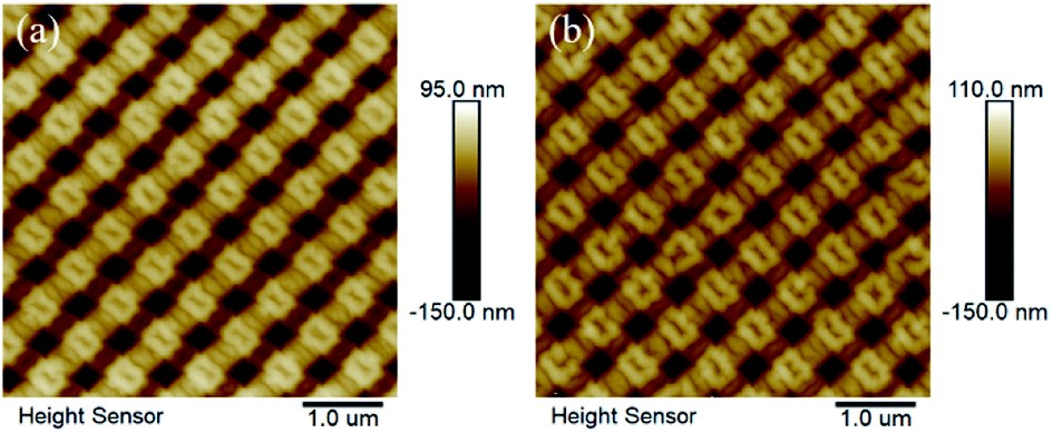 | ||
| Fig. 3 AFM images of multiscale grid/wrinkle PDMS films with etching times of (a) 30 s and (b) 60 s. | ||
In order to investigate the effectiveness of light extraction, green QLEDs were fabricated by attaching the nanostructured PDMS films on the ITO–glass substrate. Fig. 4 displays the performance characteristics of QLEDs with and without nanostructured PDMS which are tested by PR-735. As shown in Fig. 4(a) the turn on voltages of both QLEDs with and without PDMS nanostructures are about 2.2 V, and also the current density–voltage (J–V) characteristics remains unchanged which indicates that attaching nanostructured PDMS has no effect on the electrical performance of the devices. The luminance of the nanostructured device is about 178700 cd m−2, which is about 46% higher than that of the controlled QLEDs (122400 cd m−2) under the same driving voltage. The EQE and current efficiency (CE) of the controlled and nanostructured QLEDs are shown in Fig. 4(b) which clearly demonstrates the large enhancement of both values after introducing the nanostructured PDMS film outside the QLEDs. Table 1 summarizes the performance of QLEDs with and without nanostructured PDMS films, and the luminance (178700 cd m−2), current efficiency (70.38 cd A−1) and EQE (17.87%) values of the QLEDs with nanostructured PDMS are all 1.46 times than those of the controlled QLEDs. The highest EQE and CE values of QLEDs with nanostructured PDMS are significantly improved to 21.3% and 88.3 cd A−1 which are 1.7 times higher than those of the controlled QLEDs. Fig. 4(c) compares the normalized EL spectra at the same driving voltage of 4 V for the controlled and nanostructured devices; the peak position is kept at 526 nm and the intensity is improved greatly. The inserted pictures in Fig. 4(c) indicated, at the same driving voltages, the nanostructured QLEDs showing much brighter features. Fig. 4(d) shows normalized EL intensities at observation angles from 0° to 90°, in which the black dotted line is the Lambert emission spectrum. At a bias voltage of 3.4 V, with the change of the observation angle, the emission spectra distribution of the device with multiscale nanostructures tend to be similar to the Lambert emission profiles. At the same time, the EL spectra of the nanostructured QLEDs are independent of the viewing angles which indicate no angular emission effect when using grid/wrinkle patterns outside the glass substrate.26,27 As for comparison, grid or wrinkle PDMS films are applied to the green QLED devices under the same voltage and current density. As shown in Fig. S3 and S4,† the grid PDMS nanostructure makes the brightness of the device increase from 151500 cd m−2 to 155900 cd m−2, with about 3% improvement, and the current efficiency of the device increases from 41.37 cd A−1 to 42.29 cd A−1. The grid structure here extract little light out of the ITO substrate and behaves angle dependent.28 The wrinkle PDMS nanostructure increases the brightness of the device from 151000 cd m−2 to 154900 cd m−2, and the current efficiency from 42.09 cd A−1 to 48.88 cd A−1. Compared with the electroluminescence spectra of the green QLED with or without wrinkle nanostructures, the wrinkle ones can also enhance the EL intensity of devices. As an aperiodic nanostructure, the wrinkle nanostructure tends to comply Lambert emission at the observation angle. Here, the wrinkle structure is randomly formed and does not have directionality, which can reduce the angle dependence under a wide observation angle and effectively increase the visual angle of the QLED.29
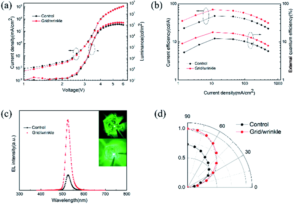 | ||
| Fig. 4 Performance characteristics of the control and nanostructured green-emission QLED. (a) Current density–luminance–voltage characteristics. (b) Current efficiency and external quantum efficiency as a function of current density. (c) Normalized EL spectra. The insets in (c) depict the photographs of the fabricated QLEDs with and without PDMS nanostructures, respectively. (d) Normalized EL spectra with different viewing angles. | ||
| Device structure | L max (cd m−2) | η CE (cd A−1) | η PE (lm W−1) | η EQE (%) | |||
|---|---|---|---|---|---|---|---|
| Max | @1000 cd m−2 | Max | @1000 cd m−2 | Max | @1000 cd m−2 | ||
| Control | 122400 |
48.02 | 20.62 | 41.90 | 23.14 | 12.29 | 5.28 |
| Grid/wrinkle | 178700 |
70.38 | 36.13 | 61.42 | 36.93 | 17.94 | 9.25 |
| Enhancement | 1.46 | 1.46 | 1.75 | 1.46 | 1.59 | 1.46 | 1.75 |
In order to illustrate the repeatability of light output enhancement of QLEDs after introducing multiscale PDMS nanostructures, 30 groups of nanostructured QLEDs were counted. The EQE histograms show the high reproducibility of both the nanostructured and controlled QLEDs. Since the performances of the controlled QLEDs are constant, the performance improvement of the nanostructured QLEDs is confirmed through the enhanced outcoupling efficiency of the total internal reflection light. As shown in Fig. 5, the average peak EQE of the patterned QLEDs is 17.61%. These results fully prove the authenticity of the experiment. In addition, the highest EQE is about 21.3%, which is the best value for green QLEDs with light outcoupling nanostructures, to the best of our knowledge. The introduction of multiscale grid/wrinkle nanostructures greatly improves the efficiency of the device, which indicates broad prospects for the practical application of this method.
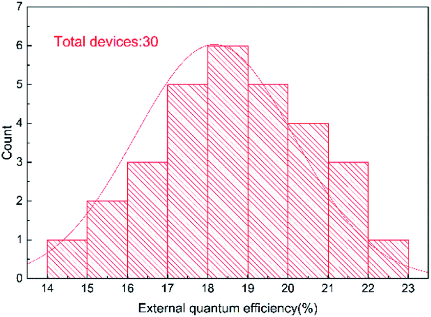 | ||
| Fig. 5 Histogram EQE of nanostructured QLEDs. | ||
Theoretical simulations are carried out for the in-depth study of the mechanism of light extraction by multiscale nanostructures. The simulations are based on the finite-difference-time-domain (FDTD) method by simulating the near-field light propagation outside the devices. Due to the peak position of the green QLED at 526 nm, one dipole light source with the horizontal orientation at a wavelength of 526 nm is placed in the QD emitting layers to analyse the light outcoupling behaviors in the QLED.30,31Fig. 6 demonstrates the distribution of the transverse electric polarized light in controlled and nanostructured QLEDs with the simulated cross-section views of the near-field intensities. From the distribution of the electromagnetic field, it can be seen that the total reflection phenomenon is more intuitively between the glass and air interface layer. This is due to the large difference of the refractive index between the glass substrate and the air medium.32,33 Compared with the controlled device, a large amount of the internally confined light will be effectively extracted from the glass substrate due to the attaching of multiscale PDMS nanostructures. Fig. 6(b) and (c) show the distribution of the electromagnetic field in QLEDs with grid and wrinkle nanostructures, respectively. The introduction of grid or wrinkle nanostructures could only increase the total reflection angle of light in QLEDs with moderate ratios. Fig. 6(d) reveals the distribution of the electromagnetic field in the QLEDs with multiscale PDMS nanostructures. The multiscale nanostructure takes advantages of both grid and wrinkle nanostructures. It not only increases the total reflection angle of photons in the device, but also enhances the distribution of the electromagnetic field at the air interface.34,35 The detailed image of the field intensity at the ITO/air interface also indicated that the multiscale nanostructure is much more effective in light extraction which can increase the total reflection angle of QLEDs. At the same time, the transmission spectrum of the controlled and optimized device also shows that in the green band, the transmission increases from 88.01% to 90.48% which is consistent with the results of theoretical simulation (Fig. S5†).
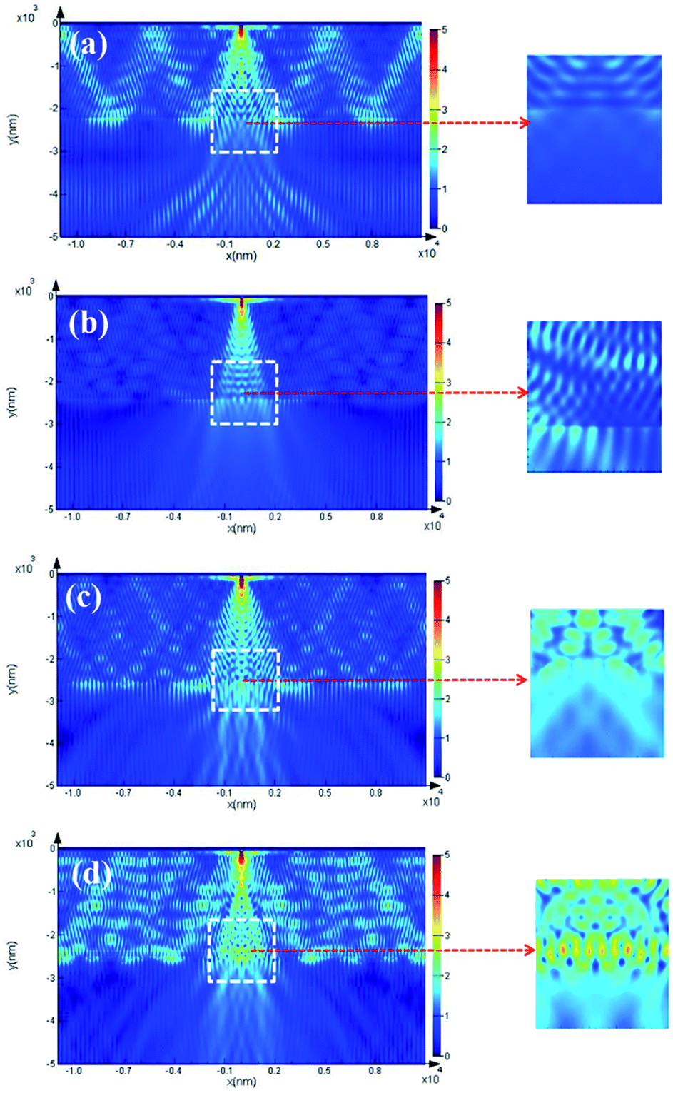 | ||
| Fig. 6 Calculated distribution of the power near field intensity at the interface between ITO glass and air without (a) and with (b) grid nanostructures at a wavelength of incident polarized light of 526 nm (c) wrinkle nanostructure and (d) multiscale grid/wrinkle nanostructures. Enlargement: detail image of field intensity at the interface between ITO glass and air without and with PDMS nanostructures. | ||
Conclusions
In summary, high-performance green QLED devices have been achieved by introducing nanostructured PDMS films outside the QLEDs for efficient outcoupling of total internal reflection light. The multiscale PDMS has the advantage of periodic and randomly distributed nanostructures for light extraction. By attaching outside light outcoupling structures on ITO glass, a large amount of the trapped light could be extracted and total reflection is decreased, which dramatically enhances the maximum EQE and luminance for green QLEDs. The result indicates that QLEDs with multiscale outcoupling structures exhibit the highest EQE of 21.3% and a current efficiency of 88.3 cd A−1. Furthermore, the multiscale nanostructure proposed here can maintain the emission profile to comply with the Lambertian radiation pattern. This method introduces outside multiscale nanostructures for further improving the efficiency of QLEDs and can promote their application in the display and lighting industries.Conflicts of interest
The authors declare no competing financial interest.Acknowledgements
This work is supported by National Natural Science Foundation of China (Grant No. 61376061, 11274093, 51572070, U1604261, 61605041, U1204208), Program for Changjiang Scholars and Innovative Research Team in University (No. PCSIRT15R18). Shujie Wang, and Chenran Li contributed equally to this work.References
- Y. Shirasaki, G. J. Supran, M. G. Bawendi and V. Bulović, Nat. Photonics, 2013, 7, 13–27 CrossRef CAS.
- Y. E. Panfil, M. Oded and U. Banin, Angew. Chem., Int. Ed., 2018, 57, 4274–4295 CrossRef CAS PubMed.
- X. Dai, Y. Deng, X. Peng and Y. Jin, Adv. Mater., 2017, 29, 1607022 CrossRef PubMed.
- X. Li, Y. B. Zhao, F. Fan, L. Levina, M. Liu, X. Gong, L. Quan, J. Fan, Z. Yang, S. Hoogland, O. Voznyy, Z. Lu and E. H. Sargent, Nat. Photonics, 2018, 12, 159–164 CrossRef CAS.
- H. Shen, Q. Gao, Y. Zhang, Y. Lin, Q. Lin, Z. Li, L. Chen, Z. Zeng, X. Li, Y. Jia, S. Wang, Z. Du, L. Li and Z. Zhang, Nat. Photonics, 2019, 13, 192–197 CrossRef CAS.
- X. Dai, Z. Zhang, Y. Jin, Y. Niu, H. Cao, X. Liang, L. Chen, J. Wang and X. Peng, Nature, 2014, 515, 96–99 CrossRef CAS PubMed.
- L. Wang, J. Lin, Y. Hu, X. Guo, Y. Lv, Z. Tang, J. Zhao, Y. Fan, N. Zhang, Y. Wang and X. Liu, ACS Appl. Mater. Interfaces, 2017, 9, 38755–38760 CrossRef CAS PubMed.
- Y. Sun, Y. Jiang, X. W. Sun, S. Zhang and S. Chen, Chem. Rec., 2019, 19, 1–25 CrossRef PubMed.
- R. Zhu, Z. Luo and S. T. Wu, Opt. Express, 2014, 22, A1783–A1798 CrossRef CAS PubMed.
- J. Feng, Y. F. Liu, Y. G. Bi and H. B. Sun, Laser Photonics Rev., 2015, 11, OT1A.1 Search PubMed.
- Y. H. Kim, J. Lee, W. M. Kim, C. Fuchs, S. Hofmann, H. W. Chang, M. Gather, L. Müller-Meskamp and K. Leo, Adv. Funct. Mater., 2014, 24, 2553–2559 CrossRef CAS.
- Y. Qu, M. Slootsky and S. R. Forrest, Nat. Photonics, 2015, 9, 758–763 CrossRef CAS.
- H. Y. Xiang, Y. Q. Li, L. Zhou, H. J. Xie, C. Li, Q. D. Ou, L. S. Chen, C. S. Lee, S. T. Lee and J. X. Tang, ACS Nano, 2015, 9, 7553–7562 CrossRef CAS PubMed.
- R. Yu, F. Yin, X. Huang and W. Ji, J. Mater. Chem. C, 2017, 5, 6682–6687 RSC.
- S. Wang, X. Dou, L. Chen, Y. Fang, A. Wang, H. Shen and Z. Du, Nanoscale, 2018, 10, 11651–11656 RSC.
- K. Ding, Y. Fang, S. Dong, H. Chen, B. Luo, K. Jiang, H. Gu, L. Fan, S. Liu, B. Hu and L. Wang, Adv. Opt. Mater., 2018, 6, 1800347 CrossRef.
- Q. Zhang, X. Gu, Z. Chen, J. Jiang, Z. Zhang, J. Wei, F. Li, X. Jin, Y. Song and Q. Li, Opt. Express, 2017, 25, 17683–17694 CrossRef CAS PubMed.
- L. Zhou, X. Dong, Y. Zhou, W. Su, X. Chen, Y. Zhu and S. Shen, ACS Appl. Mater. Interfaces, 2015, 7, 26989–26998 CrossRef CAS PubMed.
- H. D. Li, C. S. Hsu, F. M. Zhan and Y. C. Chao, ACS Appl. Mater. Interfaces, 2015, 7, 7462–7465 CrossRef CAS PubMed.
- H. K. Raut, S. Dinachali, Y. C. Loke, R. Ganesan, K. K. Ansah-Antwi, A. Góra, E. H. Khoo, V. Ganesh, M. S. Saifullah and S. Ramakrishna, ACS Nano, 2015, 9, 1305–1314 CrossRef CAS PubMed.
- Y. D. Kim, K. Kim, M. S. Byun, H. J. Choi and H. Lee, J. Appl. Phys., 2017, 56, 06GA04 CrossRef.
- S. Jiang, Y. Feng, Z. Chen, L. Zhang, X. Jiang, Q. Jiao, J. Li, Y. Chen, D. Li, L. Liu, T. Yu, B. Shen and G. Zhang, Sci. Rep., 2016, 6, 21573 CrossRef CAS PubMed.
- Y. Yang, Y. Zheng, W. Cao, A. Titov, J. Hyvonen, J. R. Manders, J. Xue, P. H. Holloway and L. Qian, Nat. Photonics, 2015, 9, 259–266 CrossRef CAS.
- H. G. Park, H. C. Jeong, Y. H. Jung and D. S. Seo, Sci. Rep., 2015, 5, 12356 CrossRef.
- H. C. Jeong, H. G. Park, Y. H. Jung, J. H. Lee, B. Y. Oh and D. S. Seo, Langmuir, 2016, 32, 7138–7143 CrossRef CAS.
- M. Kovačic, P. A. Will, B. Lipovsek, M. Topic, S. Lenk, S. Reineke and J. Krc, ACS Photonics, 2018, 5, 422–430 CrossRef.
- J. H. Kim, L. Do, J. Choi and J. Park, Opt. Lett., 2013, 38, 3773–3775 CrossRef CAS PubMed.
- G. Zhang, X. Guo, F. F. Ren, Y. Li, B. Liu, J. Ye, H. Ge, Z. Xie, R. Zhang, H. Tan and C. Jagadish, ACS Photonics, 2016, 3, 1912–1918 CrossRef CAS.
- H. Cho, E. Kim, J. Moon, C. Joo, E. Kim, S. Park, J. Lee, B. Yu, J. I. Lee and S. Yoo, Org. Electron., 2017, 46, 139–144 CrossRef CAS.
- R. Zhu, Z. Luo and S. T. Wu, Opt. Express, 2014, 22, A1783–A1798 CrossRef CAS PubMed.
- A. I. Zhmakin, Phys. Rep., 2011, 498, 189–241 CrossRef CAS.
- A. Salehi, X. Fu, D. Shin and F. So, Adv. Funct. Mater., 2019, 29, 1808803 CrossRef.
- S. Jeon, L. Zhao, Y. J. Jung, J. Kim, S. Y. Kim, H. Kang, J. H. Jeong, P. B. Rand and J. H. Lee, Small, 2019, 15, 1900135 CrossRef PubMed.
- L. H. Xu, Q. D. Ou, Y. Q. Li, Y. B. Zhang, X. D. Zhao, H. Y. Xiang, J. D. Chen, L. Zhou, S. T. Lee and J. X. Tang, ACS Nano, 2015, 10, 1625–1632 CrossRef PubMed.
- Q. Zhang, M. M. Tavakoli, L. Gu, D. Zhang, L. Tang, Y. Gao, J. Guo, Y. Lin, S. F. Leung, S. Poddar, Y. Fu and Z. Fan, Nat. Commun., 2019, 10, 727 CrossRef PubMed.
Footnote |
| † Electronic supplementary information (ESI) available. See DOI: 10.1039/d0na00150c |
| This journal is © The Royal Society of Chemistry 2020 |