
 Open Access Article
 This Open Access Article is licensed under a Creative Commons Attribution-Non Commercial 3.0 Unported Licence
Flexible nanophosphor films doped with Mie resonators for enhanced out-coupling of the emission†
José M.
Miranda-Muñoz
 ,
Dongling
Geng
,
Mauricio E.
Calvo
,
Gabriel
Lozano
* and
Hernán
Míguez
,
Dongling
Geng
,
Mauricio E.
Calvo
,
Gabriel
Lozano
* and
Hernán
Míguez
Instituto de Ciencia de Materiales de Sevilla, Consejo Superior de Investigaciones Científicas – Universidad de Sevilla (CSIC-US), Américo Vespucio 49, 41092, Seville, Spain. E-mail: g.lozano@csic.es
First published on 7th December 2018
Abstract
Herein, we present a general method to prepare self-standing flexible photoluminescent coatings of controlled opacity for integration into light-emitting diodes (LEDs) employing cost-effective solution-processing methods. From colloidal suspensions of nano-sized phosphors, we fabricate light-emitting transparent films that can be doped with spherical scatterers, which act as Mie resonators that trigger a controlled photoluminescence enhancement, evidenced by the reduction of the guided light along the layer. This results in an enhanced emission compared to that extracted from a bare phosphor layer. We show not only that emission is visible under ultraviolet-LED illumination for both rigid and flexible versions of the coatings, but we also prove the feasibility of the integration of these flexible conversion layers into such devices. We believe these results can contribute to develop more efficient and cost-effective illumination sources by providing efficient and easy-to-handle conversion layers susceptible to excitation by LEDs emitting at wavelengths in the near UV region.
Introduction
With light emitting diodes (LEDs) taking over the illumination market, the optimization of their optical and electrical properties has arisen as a concern of utter importance, in order to fully realize their potential as artificial light sources. Their advantageous properties in relation to conventional light sources, such as robustness, longer lifetimes, possibility of colour tuning or lower power consumption, present them as an exceptional alternative to their incandescent counterparts.1–3 Commercial LEDs typically rely upon blue or UV diodes for the generation of light,2,4–8 therefore requiring a conversion layer for the downshifting of this radiation at wavelengths suitable for illumination applications. To that regard, rare-earth (RE)-doped materials have been intensively studied for colour conversion.6,8,9 In this context, polymer embedding of RE phosphors is a route commonly employed to build versatile and adaptable colour converting coatings for LED technology.10–12 As phosphor crystal sizes are typically in the range of the few microns, these composite films, commonly found in commercial lamps, are opaque, which implies some drawbacks. On the one hand, opacity limits their application as transparent emissive screens and hence their use in displays. On the other, for those applications in which opacity is not a problem, it hinders the possibility to controllably tune the out-coupling of light from the device, which is recognized as one the most critical sources of efficiency loss in LEDs.13,14 In this latter context, the fraction of emitted light that can be extracted from a film is seriously reduced by the phenomenon of total internal reflection, causing partial trapping of light inside the layer, which escapes through the edges. In order to solve this issue, different approaches based on the controlled introduction of scattering have been employed for different types of light-emitting devices.15–22 The use of metallic particles for the emission enhancement of emitters has been previously reported;23–27 notwithstanding, these are expected to yield larger absorption losses than their dielectric counterparts in the range of excitation of the phosphors.28 For the case of RE-based LEDs, the problem has been thoroughly analysed,29 but the above-mentioned limitations imposed by the materials employed have impeded the development of novel ways to tune and enhance the out-coupling.In this work, we present a procedure for fabricating a flexible nanophosphor-based light emitting material, which can be designed either to be fully transparent or to present a controlled opacity. These materials allow the introduction of random inclusions of crystalline titanium dioxide (TiO2) microspheres as a means to controllably increase the amount of emitted light that can be extracted. Owing to the scattering triggered by the presence of TiO2 spheres of controlled size and concentration, light is offered several opportunities to reach the layer–air interface along a direction within the solid angle defined by the critical angle and thus contribute to the total usable light. The emission enhancement is directly related to the scattering mean free path (lsc) values expected from Mie theory applied to the titania resonators embedded in originally transparent phosphor film. We show the general character of this approach by applying it to different kinds of RE-doped phosphors.
Results and discussion
Paste preparation and material fabrication
Crystalline gadolinium vanadate matrices (GdVO4) doped with Bi3+ and Eu3+ (GdVO4:Bi3+,Eu3+) of a size around 40 nm were employed as emitting material. A sequential procedure based on solution-processing methods for the fabrication of a flexible nanophosphor layer starting from a liquid dispersion of such emitters was developed, as presented in Fig. 1. In order to fabricate layers with thicknesses of few microns, a viscous paste based on the synthesized nanophosphors was prepared. From an initial dispersion of the emitters in methanol, a procedure of tip sonication and addition of organic binders and a solvent described in the experimental section yielded a viscous dispersion after removal of methanol via distillation, as shown in Fig. 1(a). A sacrificial layer underneath the emitting film was required for the fabrication of a flexible self-standing version. To that aim, glass or quartz substrates were coated with a dense solid SiO2 layer according to the description included in the experimental section, Fig. 1(b). On top of the SiO2-coated substrate, a layer was deposited from the previously prepared viscous paste employing the technique of doctor blade, as displayed in Fig. 1(c). Both mechanical stabilization and removal of the organic components of the layer were attained through sequential heating stages. Further details are provided in the experimental section of the work. As a consequence, a rigid emitting layer resulted. Owing to the high porosity of the nanophosphor matrix, the material was susceptible to be endowed with flexibility through infiltration with a polymer.30 In our case, a solution of poly(methyl methacrylate), PMMA, was infiltrated by spin coating, followed by a drying process, as shown in Fig. 1(d). A last step of etching of the SiO2 coating was required for removal of the flexible nanophosphor layer from the substrate. With that purpose, the system was immersed in a HF solution, causing detachment of the flexible film from the solid substrate due to etching of the dense SiO2 layer without compromising the polymer and yielding a flexible self-standing film incorporating the photoluminescent material, Fig. 1(e).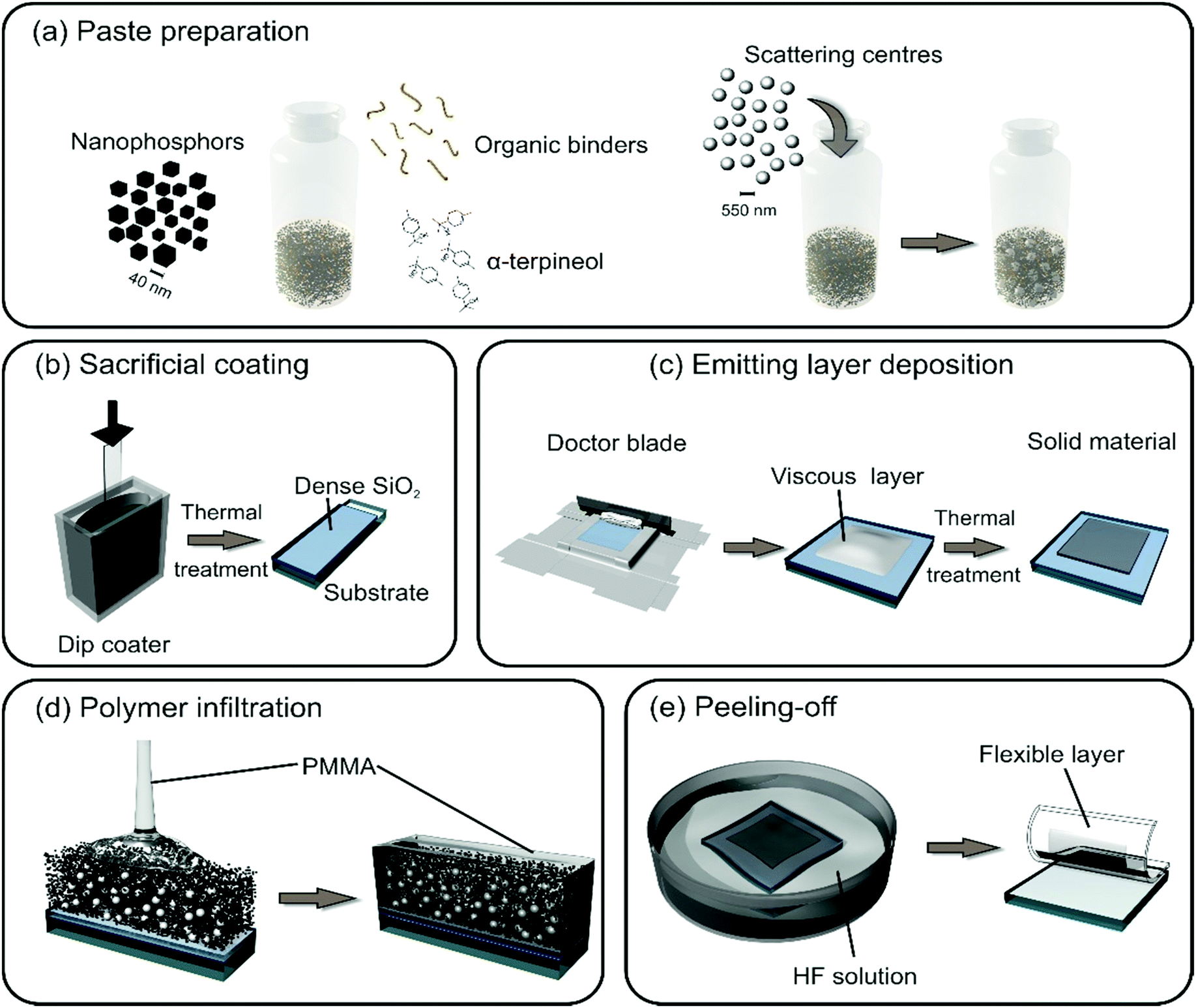 | ||
| Fig. 1 Description of the different steps of preparation and fabrication of a flexible photoluminescent nanophosphor-based material with and without the inclusion of scattering centres from an initial dispersion of nanophosphors. | ||
Transparent and flexible light-emitting nanophosphor layer
Crystalline nanophosphors consisting of a gadolinium vanadate matrix co-doped with trivalent cations of bismuth and europium (GdVO4:Bi3+,Eu3+) with an average size of (36 ± 7) nm were synthesized following a procedure already reported,31 as visible in the Transmission Electron Microscopy (TEM) image displayed in Fig. 2(a). Comparison with phosphors devoid of Bi3+ cations highlights that the doping of the GdVO4 matrix with Bi3+ yielded a cubic shape of the crystals. The crystallinity of the nanophosphors was confirmed by the X-ray diffraction (XRD) pattern presented in Fig. 2(b), demonstrating their crystallization into the tetragonal GdVO4 structure when compared to the standard PDF 86-0996, ICDD 2014 reference. The estimated crystallite size of 39.5 nm derived from the Scherrer formula is in fair agreement with that obtained from the analysis of TEM images. Following the procedure depicted in Fig. 1, emitting matrices, such as the layer displayed in the SEM image in Fig. 2(c), were fabricated employing the crystalline nanophosphors as base material. We concluded that a thickness around 4 μm was enough so as to ensure full extinction of the incident light at the wavelength of interest, namely, λpump = 365 nm, and was therefore established as standard thickness for the layers fabricated and studied in this work. Specifically, a 4 μm thick layer could absorb up to 76% of the incident radiation at this wavelength, as shown in the absorption spectrum displayed in the ESI,† Fig. S1. Because highest brightness in the layers is sought for, larger thicknesses would result detrimental for this purpose, since no light would remain available to be further absorbed in the material beyond the penetration depth at the wavelength of interest. The emission properties of this layer are displayed in Fig. 2(d). The excitation spectrum displays an intensity peak below 300 nm that originates from a charge transfer from the oxygen ligands to the vanadium atom of the VO43− group, and a broad decay up to 400 nm owing to an energy transfer from the Bi3+ to Eu3+. This decay is considered a broadening of the excitation spectrum when compared to that of phosphors without Bi3+. The co-doping with Bi3+ enables therefore excitation in the UVA region of the electromagnetic spectrum. Direct excitation of the Eu3+ cations is also possible, yet not visible in the spectrum as a consequence of their low absorption cross section in comparison to GdVO4:Bi3+ matrix-mediated excitation. The photoluminescence (PL) spectrum shows the most significant emission line at λ = 617 nm, a narrow emission peak originating from the electric-dipole transition 5D0 → 7F2 of Eu3+ ions. The high optical transparency – see Fig. 2(e) – in the visible range of 4 μm thick layers of this material is due to the nanometric size of the phosphors. Intense red photoluminescence is triggered under UV-light irradiation, as visible in panel (f) for both versions of the material, rigid and flexible. Thus, we have demonstrated the feasibility of a transparent emitting layer based on nano-sized phosphors, enabling strong red photoluminescence when excited at wavelengths in the UVA region, i.e. λpump > 350 nm. The described fabrication process is general enough to enable extension to crystalline nanophosphors doped with a different RE cation. In effect, we employed GdVO4:Bi3+ matrices doped with trivalent Dy3+ cations for the fabrication of rigid and flexible photoluminescent layers showing yellowish emission, as visible in the Fig. S2 in the ESI.†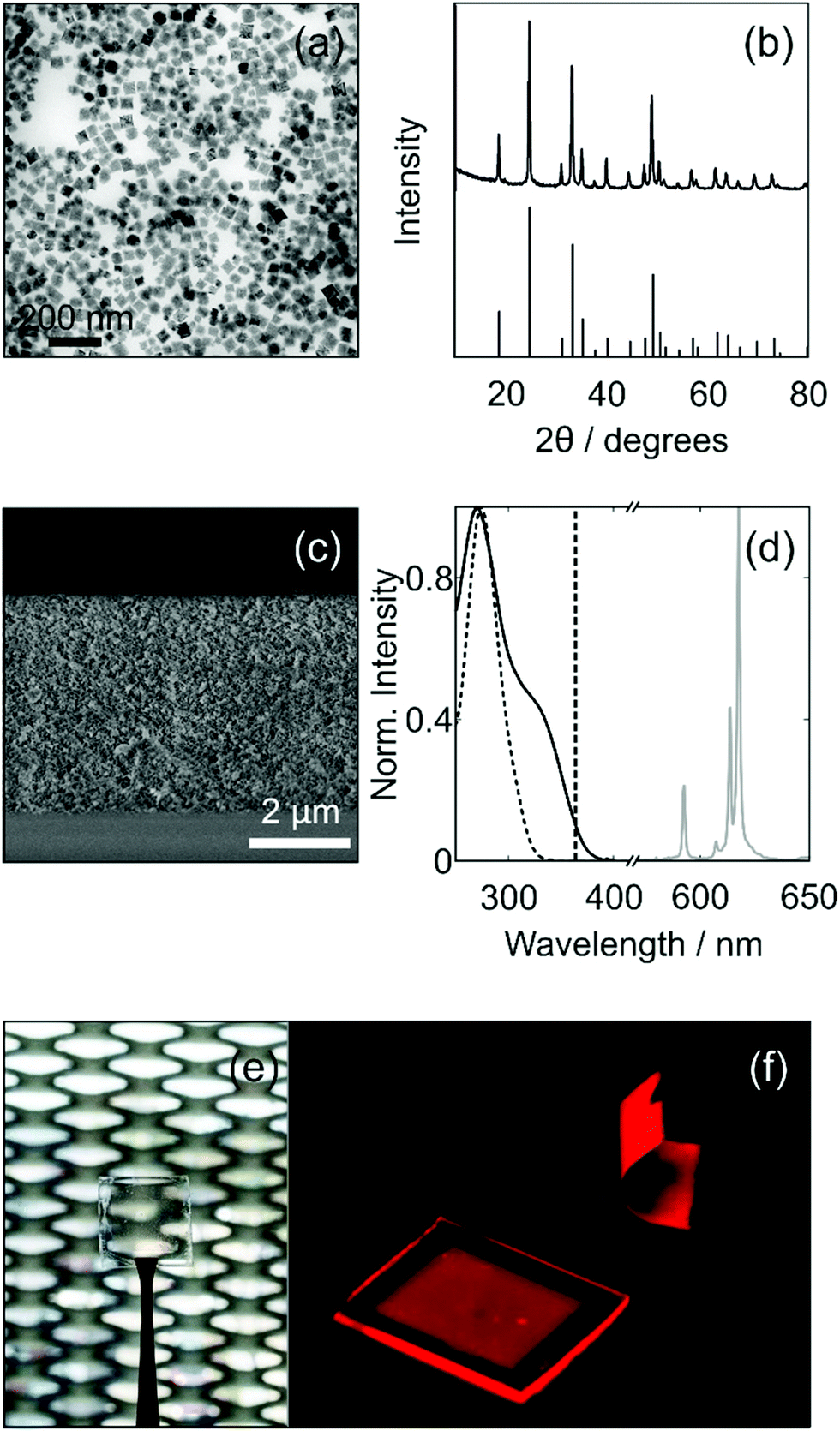 | ||
| Fig. 2 (a) Transmission Electron Microscopy (TEM) image of the synthesized GdVO4:Bi3+,Eu3+ phosphors. (b) X-ray diffraction (XRD) diagram obtained for dry GdVO4:Bi3+,Eu3+ powder. The standard PDF 86-0996, ICDD 2014 reference is included (lower half) for comparison. (c) Scanning Electron Microscopy (SEM) cross section of a nanophosphor layer fabricated employing the procedure previously described. (d) Normalized excitation (black curve) and photoluminescence (PL) spectrum (grey curve) of a nanophosphor layer. The black-dashed curve represents the normalized excitation spectrum of phosphors devoid of bismuth cations. The black-dashed line indicates the pumping wavelength used in this work, namely, λpump = 365 nm. (e) Picture of a 4 μm nanophosphor layer. The material displays high transparency in the visible range of the spectrum. (f) Picture of a rigid and flexible nanophosphor layer under UV irradiation. Energy transfer from the GdVO4 matrix to the Eu3+ cations is evidenced by the visible red intense emission. | ||
Mie scatterers improve out-coupling
In order to enhance the photoluminescence of the prepared flexible nanophosphor films, we propose the inclusion of optical disorder in the emitting matrices, based on the previous observation of an improvement of the extraction of the emitted light in a similar material due to the presence of scattering centres.32 In that way, light is offered a higher probability to be out-coupled from the film, which would otherwise remain trapped inside by means of total internal reflection. Since the thickness of the material was chosen for optimum absorptance at the pumping wavelength, any appreciable photoluminescence enhancement could be claimed to mostly derive from a reduction of the guiding of the emitted light along the layer and not to an enhancement of the light harvesting efficiency. As scattering elements, nanocrystalline anatase spheres of radius r = (225 ± 20) nm were synthesized and employed. A Scanning Electron Microscopy (SEM) image of these crystalline spheres has been included in the ESI,† Fig. S3. In order to integrate such scatterers in the material, they were added to the nanophosphor paste during the paste preparation process described in Fig. 1(a), as reported somewhere else.32 The resulting medium consisted of a porous nanophosphor layer presenting a random distribution of crystalline TiO2 nanospheres with controlled size and concentration. A cross-section SEM image of a material in which scattering centres with a volume concentration of 10% is shown in Fig. 3(a). As we aimed at establishing a dependence between the emission improvement and the amount of included optical disorder, different scatterer concentrations were tested, namely, 5%, 10%, 12% and 15%. As a previous step to this study, we performed calculations of one of the most commonly employed magnitudes for the characterization of optically disordered media, specifically, the scattering mean free path, lsc. The scattering centre concentrations were considered to be low enough as to assume the optical behaviour of the layers is dictated only by single-particle considerations according to Mie formalism, following the procedure depicted elsewhere.32 Specifically, a porous nanophosphor matrix with a 50% porosity was considered as the external medium, whereas stratified TiO2–air spherical structures were included as scattering centres, taking 0.43r as the thickness of the air layer according to experimental observations, where r refers to the radius of the TiO2 spheres. The optical constants employed for both materials have been included in the ESI,† Fig. S4. Fig. 3(b) displays the spectral lsc yielded by these calculations. An increase in the concentration of scattering spheres leads to lower values of lsc, namely, higher scattering strength, as we could have anticipated. As a consequence of the inclusion of optical disorder, light partially propagates in a diffusive manner throughout the material, leading to higher opacity, as qualitatively displayed in Fig. 3(c). An increase of the scatterer concentration in the nanophosphor film yields a gradual reduction of its transparency, Fig. 3(d), further confirming the trend displayed by the calculated lsc spectra presented in Fig. 3(b). Indeed, when comparing the nanophosphor film with and without scattering centres – see Fig. 3(c) and 2(e), we can confirm that, whereas light is mostly ballistically transmitted through the latter, the presence of optical disorder in the former triggers the diffusive propagation of light, granting it with a whitish appearance typical of turbid media.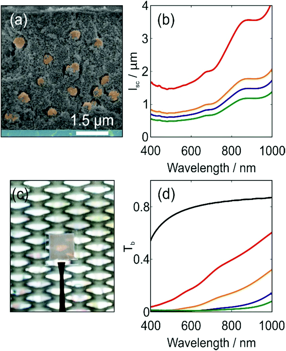 | ||
| Fig. 3 (a) SEM cross section of a nanophosphor matrix including spherical TiO2 scattering centres in a 10% volume filling fraction. Different materials have been artificially shaded with colour for the sake of clarity. (b) Scattering mean free path, lsc, spectra calculated employing Mie formalism for systems including scattering centres in a 5% (red curve), 10% (orange curve), 12% (blue curve) and 15% (green curve) concentration. (c) Picture of a 4 μm nanophosphor layer including TiO2 spheres with a 5% volume filling fraction. The inclusion of scattering centres triggers diffuse propagation of the light. (d) Ballistic transmittance for a reference layer (black curve) and for layers including scattering centres in a 5% (red curve), 10% (orange curve), 12% (blue curve) and 15% (green curve) concentration. | ||
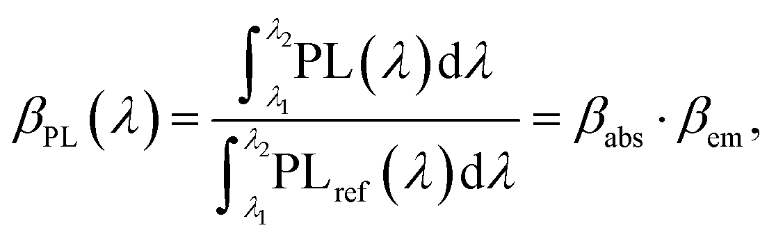
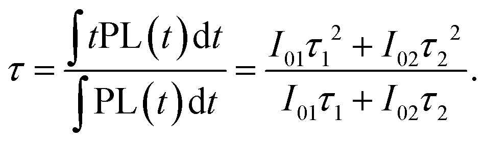
A study related to the PL of the material was performed in order to assess the effect of the random inclusion of scattering centres in the nanophosphor matrix on its emission properties. Since the photoluminescence properties of the material remain virtually invariable from the rigid to the flexible film infiltrated with PMMA, as demonstrated by the PL spectra included in the ESI,† Fig. S5, the PL study has been performed on rigid samples for the sake of experimental ease. Information regarding the PL spectra is displayed in the colour map of Fig. 4(a). Here, a constant increase in the total emission with respect to the layer devoid of scattering centres is generally observed, especially noticeable at the emission peak around λ = 617 nm. Maximum luminescence occurs for the material with 12% scattering centre filling fraction, whereas it decreases for a higher concentration, namely, 15%. Quantification of the photoluminescence enhancement is displayed in Fig. 4(b), calculated by means of the expression:
 | (1) |
being PL(t) the time-dependent PL intensity, τ1 and τ2 the short and the long decay components, respectively, and I01 and I02 the amplitudes of each term of the fitting. The long component of the decay is generally associated with the transition of Eu3+ cations that sit in the bulk of the nanoparticle, whereas the short component refers to the transition of cations close to the surface of the nanoparticle. The average lifetimes corresponding to the collected decays are visible in Fig. 4(d) and have been calculated by means of:
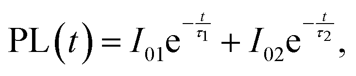
The fitting curves and fitting parameters are included in the Fig. S6, ESI.† As visible in Fig. 4(d), the value of the average lifetime remains virtually unchanged for the material with a 5% scattering centre filling fraction with respect to the reference matrix. This proves that the inclusion of scattering centres hardly has an influence on the processes involved in the photoluminescence of the phosphors, as expected. Although a slight decrease is noticeable for higher concentrations, the average lifetime value falls off significantly when a 15% scattering particle filling fraction is considered, in accordance with the PL enhancement trend. We attributed this decay to the high sensitivity of the nanophosphor surface conditions on their photoluminescence performance. The medium surrounding the phosphor nanocrystals have been proven to have a relevant impact on the emission properties,33–35 thus affecting their dynamic emission characteristics. Whereas the presence of TiO2 scattering centres did not appear to relevantly modify the photonic environment for a change in the intrinsic emission properties of the nanophosphors, scattering centres in concentrations above 12% started to be perceptible by the nanophosphors, affecting their photoluminescence. Nonetheless, the adverse effect of the inclusion of scattering centres is not revealed as significant for volume filling fractions below 15%. The images in Fig. 4(e) demonstrate the observable emission enhancement. The visible reduction of the light escaping through the edges of the substrate results in a more intense emission by the material due to an efficient out-coupling. A similar behaviour is revealed by nanophosphor-based layers including Dy3+ as the rare-earth cation, Fig. 4(f), displaying in this case a yellowish luminescence due to the main emission line around λ = 570 nm. Fig. S7 in the ESI† displays the luminescence of our flexible nanophosphor-based material under UV-LED illumination, demonstrating the potential of these conversion layers for integration into emitting devices. Besides, we have proven their suitability in terms of thermal stability, as shown in the ESI,† Fig. S8.
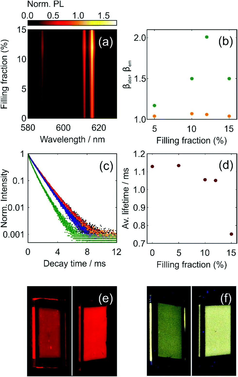 | ||
| Fig. 4 (a) PL spectra of the emitting matrices with and without scattering centres. The plotted scatterer concentration are 0%, 5%, 10%, 12% and 15%. The spectra are normalized to the maximum PL value of the reference layer. (b) Absorption (orange dots) and PL (green dots) enhancements obtained by means of expression (1) in relation to the scattering centre concentration. (c) Time-resolved PL decays for a reference layer (black decay) and layers including scattering centres with a 5% (red decay), 10% (orange decay), 12% (blue decay) and 15% (green decay) concentration. (d) Average lifetime dependence on the volume filling fraction value of the scattering centres. (e) Red luminescence of a bare nanophosphor layer (left) and of a layer including a 10% concentration of TiO2 spherical scattering centres (right). (f) GdVO4:Bi3+,Dy3+-based layers with thickness around 4 μm showing yellow luminescence under UV irradiation for a bare matrix (left) and a film integrating scattering centres in a 10% concentration (right). | ||
Conclusions
In summary, an experimental procedure based on solution-processing methods for the realization of flexible self-standing transparent phosphor-based conversion layers in a cost-effective manner was developed and demonstrated. Crystalline GdVO4:Bi3+,Eu3+ phosphors were used as photoluminescent material. The doping with Bi3+ was justified with the demonstration of a broadening of the excitation spectrum of the nanophosphors, allowing emission of the material when pumping at a wavelength above the deep UV region, λpump = 365 nm in our study. We proposed and confirmed the inclusion of optical disorder as a straightforward and easy-to-implement approach to achieve an improvement of the PL at the expense of the transparency of the film, as a consequence of a reduction of the fraction of the emitted light remaining trapped in the layer and guided through total internal reflection. The generality of the depicted procedure allows extension to other RE-based phosphors, as proved by the fabrication of flexible photoluminescent layers based on GdVO4 phosphors doped with Dy3+ cations, yielding yellowish emission. We believe this work opens the door to the fabrication of high-performance and more efficient solid-state illumination sources. The versatility of a flexible conversion layer allows a straightforward integration into LED devices, therefore reducing costs and avoiding other sophisticated integration routes.Experimental
Flexible layer fabrication
Characterization
Conflicts of interest
There are no conflicts to declare.Acknowledgements
Funding for the realization of the research herein presented was received from the European Research Council under the European Union's Seventh Framework Programme (FP7/2007–2013/ERC Grant Agreement 307081, POLIGHT), the European Union's Horizon 2020 research and innovation programme (ERC-2016-StG Grant Agreement 715832, NANOPHOM), and the Spanish Ministry of Economy and Competitiveness under Grant No. MAT2017-88584-R. JMMM acknowledges the Spanish Ministry of Education, Culture and Sport for the funding through an FPU program (FPU14/00890). DG acknowledges the funding from the Marie Curie Action MSCA-IF-2014-657434 corresponding to the European Union's Horizon 2020 Programme.Notes and references
- E. F. Schubert and J. K. Kim, Science, 2005, 308, 1274 CrossRef CAS PubMed.
- S. Pimputkar, J. S. Speck, S. P. DenBaars and S. Nakamura, Nat. Photonics, 2009, 3, 180 CrossRef CAS.
- B. Jacob, Lighting Res. Technol., 2009, 41, 291 Search PubMed.
- L. Liu, R. Xie, N. Hirosaki, Y. Li, T. Takeda, C. Zhang, J. Li and X. Sun, J. Am. Ceram. Soc., 2010, 93, 2018 CAS.
- R. Wei, C. Ma, Y. Wei, J. Gao and H. Guo, Opt. Express, 2012, 20, 29743 CrossRef CAS PubMed.
- J. Y. Tsao, M. H. Crawford, M. E. Coltrin, A. J. Fischer, D. D. Koleske, G. S. Subramania, G. T. Wang, J. J. Wierer and R. F. Karlicek Jr., Adv. Opt. Mater., 2014, 2, 809 CrossRef CAS.
- C. C. Lin and R. Liu, J. Phys. Chem. Lett., 2011, 2, 1268 CrossRef CAS PubMed.
- C. Feldmann, T. Jüstel, C. R. Ronda and P. J. Schmidt, Adv. Funct. Mater., 2003, 13, 511 CrossRef CAS.
- R. Mueller-Mach, G. Mueller, M. R. Krames, H. A. Höppe, F. Stadler, W. Schnick, T. Juestel and P. Schmidt, Phys. Status Solidi, 2005, 202, 1727 CrossRef CAS.
- M. L. Saladino, A. Zanotto, D. C. Martino, A. Spinella, G. Nasillo and E. Caponetti, Langmuir, 2010, 26, 13442 CrossRef CAS PubMed.
- A. M. Darwish, M. T. Sagapolutele, S. Sarkisov, D. Patel, D. Hui and B. Koplitz, Composites, Part B, 2013, 55, 139 CrossRef CAS.
- J. Prakash, V. Kumar, L. J. B. Erasmus, M. M. Duvenhage, G. Sathiyan, S. Bellucci, S. Sun and H. C. Swart, ACS Appl. Nano Mater., 2018, 1, 977 CrossRef CAS.
- C. Wiesmann, K. Bergenek, N. Linder and U. T. Schwarz, Laser Photonics Rev., 2009, 3, 262 CrossRef CAS.
- S. Reineke, M. Thomschke, B. Lüssem and K. Leo, Rev. Mod. Phys., 2013, 85, 1245 CrossRef CAS.
- T. Fujii, Y. Gao, R. Sharma, E. Hu, S. P. DenBaars and S. Nakamura, Appl. Phys. Lett., 2004, 84, 855 CrossRef CAS.
- J. J. Wierer, A. David and M. M. Megens, Nat. Photonics, 2009, 3, 163 CrossRef CAS.
- T. Bocksrocker, J. Hoffmann, C. Eschenbaum, A. Pargner, J. Preinfalk, F. Maier-Flaig and U. Lemmer, Org. Electron., 2013, 14, 396 CrossRef CAS.
- J. Lee, Y. Y. Kwon, E.-H. Choi, J. Park, H. Yoon and H. Kim, Opt. Express, 2014, 22, A705 CrossRef CAS.
- H. Xiang, Y. Li, L. Zhou, H. Xie, C. Li, Q. Ou, L. Chen, C. Lee, S. Lee and J. Tang, ACS Nano, 2015, 7, 7553 CrossRef PubMed.
- T. Koh, J. A. Spechler, K. M. Lee, C. B. Arnold and B. P. Rand, ACS Photonics, 2015, 2, 1366 CrossRef CAS.
- J. B. Preinfalk, T. Eiselt, T. Wehlus, V. Rohnacher, T. Hanemann, G. Gomard and U. Lemmer, ACS Photonics, 2017, 4, 928 CrossRef CAS.
- Z. Chen, L. Liang, Y. Wang, N. Qiao, J. Gao, Z. Gan and Y. Yang, J. Mater. Chem. C, 2017, 5, 1149 RSC.
- K. Okamoto, I. Niki, A. Shvartser, Y. Narukawa, T. Mukai and A. Scherer, Nat. Mater., 2004, 3, 601 CrossRef CAS.
- S. Pillai, K. R. Catchpole, T. Trupke, G. Zhang and M. A. Green, Appl. Phys. Lett., 2006, 88, 161102 CrossRef.
- O. L. Muskens, V. Giannini, J. A. Sánchez-Gil and J. G. Rivas, Nano Lett., 2007, 7, 2871 CrossRef CAS.
- J. DiMaria, E. Dimakis, T. D. Moustakas and R. Paiella, Appl. Phys. Lett., 2013, 103, 251108 CrossRef.
- G. Lozano, D. J. Louwers, S. R. K. Rodriguez, S. Murai, O. T. A. Jansen and M. A. Verschuuren, and J. Gómez Rivas, Light: Sci. Appl., 2013, 2, e66 CrossRef.
- P. Ding, M. Li, J. He, J. Wang, C. Fan and F. Zeng, Opt. Express, 2015, 23, 21477 CrossRef CAS.
- V. Y. F. Leung, A. Lagendijk, T. W. Tukker, A. P. Mosk, W. L. Ijzerman and W. L. Vos, Opt. Express, 2014, 22, 8190 CrossRef CAS PubMed.
- M. E. Calvo, J. R. Castro-Smirnov and H. Míguez, J. Polym. Sci., Part B: Polym. Phys., 2012, 50, 945 CrossRef CAS.
- A. Escudero, C. Carrillo-Carrión, M. V. Zyuzin, S. Ashraf, R. Hartmann, N. O. Núñez, M. Ocaña and W. J. Parak, Nanoscale, 2016, 8, 12221 RSC.
- J. M. Miranda-Muñoz, G. Lozano and H. Míguez, Adv. Opt. Mater., 2017, 5, 1700025 CrossRef.
- R. S. Meltzer, Phys. Rev. B: Condens. Matter Mater. Phys., 1999, 60, R14012(R) CrossRef.
- J. Zhao, Z. Lu, Y. Yin, C. McRae, J. A. Piper, J. M. Dawes, D. Jin and E. M. Goldys, Nanoscale, 2013, 5, 994 Search PubMed.
- T. Senden, F. T. Rabouw and A. Meijerink, ACS Nano, 2015, 9, 1801 CrossRef CAS.
- Y. J. Kim, M. H. Lee, H. J. Kim, G. Lim, Y. K. Choi, N. Park, K. Kim and W. I. Lee, Adv. Mater., 2009, 21, 1 Search PubMed.
- J. M. Miranda-Muñoz, S. Carretero-Palacios, A. Jiménez-Solano, Y. Li, G. Lozano and H. Míguez, J. Mater. Chem. A, 2016, 4, 1953 RSC.
Footnote |
| † Electronic supplementary information (ESI) available: Optical constants of materials employed in the calculations, spectroscopic characterization of the base material, steady-state and time-dependent photoluminescence of flexible films, and pictures of the emission under LED excitation. See DOI: 10.1039/c8tc05032e |
| This journal is © The Royal Society of Chemistry 2019 |