
 Open Access Article
 This Open Access Article is licensed under a Creative Commons Attribution-Non Commercial 3.0 Unported Licence
High-performance supercabatteries using graphite@diamond nano-needle capacitor electrodes and redox electrolytes†
Siyu
Yu‡
ab,
Kamatchi Jothiramalingam
Sankaran‡
 cd,
Svetlana
Korneychuk
e,
Johan
Verbeeck
e,
Ken
Haenen
*cd,
Xin
Jiang
*a and
Nianjun
Yang
*a
cd,
Svetlana
Korneychuk
e,
Johan
Verbeeck
e,
Ken
Haenen
*cd,
Xin
Jiang
*a and
Nianjun
Yang
*a
aInstitute of Materials Engineering, University of Siegen, Siegen 57076, Germany. E-mail: xin.jiang@uni-siegen.de; nianjun.yang@uni-siegen.de
bSchool of Chemistry and Chemical Engineering, Southwest University, Chongqing 400715, China
cInstitute for Materials Research (IMO), Hasselt University, 3590 Diepenbeek, Belgium
dIMOMEC, IMEC vzw, 3590 Diepenbeek, Belgium. E-mail: ken.haenen@uhasselt.be
eElectron Microscopy for Materials Science (EMAT), University of Antwerp, 2020 Antwerp, Belgium
First published on 6th September 2019
Abstract
Supercabatteries have the characteristics of supercapacitors and batteries, namely high power and energy densities as well as long cycle life. To construct them, capacitor electrodes with wide potential windows and/or redox electrolytes are required. Herein, graphite@diamond nano-needles and an aqueous solution of Fe(CN)63−/4− are utilized as the capacitor electrode and the electrolyte, respectively. This diamond capacitor electrode has a nitrogen-doped diamond core and a nano-graphitic shell. In 0.05 M Fe(CN)63−/4− + 1.0 M Na2SO4 aqueous solution, the fabricated supercabattery has a capacitance of 66.65 mF cm−2 at a scan rate of 10 mV s−1. It is stable over 10![[thin space (1/6-em)]](https://www.rsc.org/images/entities/char_2009.gif) 000 charge/discharge cycles. The symmetric supercabattery device assembled using a two-electrode system possesses energy and power densities of 10.40 W h kg−1 and 6.96 kW kg−1, respectively. These values are comparable to those of other energy storage devices. Therefore, diamond supercabatteries are promising for many industrial applications.
000 charge/discharge cycles. The symmetric supercabattery device assembled using a two-electrode system possesses energy and power densities of 10.40 W h kg−1 and 6.96 kW kg−1, respectively. These values are comparable to those of other energy storage devices. Therefore, diamond supercabatteries are promising for many industrial applications.
Introduction
Batteries and supercapacitors are two kinds of widely investigated and utilized electrochemical energy storage devices. A battery has a high energy density while a supercapacitor has a high power density as well as long cycle life. This difference originates from their different charge-storage mechanisms that determine their relative energy and power densities.1 Supercapacitors or electrochemical capacitors store charges either by fast ion adsorption/accumulation or by rapid faradaic reactions at the electrode/electrolyte interfaces.2,3 The former are the so-called electrical double layer capacitors (EDLCs). Due to the involvement of rapid faradaic processes (e.g., reduction/oxidation reactions and ion insertion/extraction) at or near the surface of the capacitor electrode in the latter case, such a supercapacitor is therefore labeled as a pseudocapacitor (PC).4 Although these processes occur slowly and in bulk electrode materials for batteries, a PC is still called in some cases a battery-like capacitor or a supercabattery.5–8 To construct a supercabattery, namely a supercapacitor with a large and stable capacitance (C) and high power (P) and energy (E) densities, one needs to consider carefully the employed capacitor electrode as well as the applied electrolyte.With respect to the capacitor electrode, conductive diamond synthesized using the chemical vapor deposition (CVD) technique possesses a variety of desirable features for such a goal.9–11 It is mechanically stable and chemically inert and exhibits outstanding chemical stability in harsh environments or under extreme conditions (e.g., at high current densities and potentials). Diamond supercapacitors are thus expected to be steady for longer cycle life than those fabricated from other materials. Moreover, depending on the dopants (e.g., boron, nitrogen, phosphorous, and sulfur heteroatoms), conductive diamond can be p- or n-type conductive.12,13 For example, boron-doped diamond (BDD), a p-type diamond, exhibits metal-like conductivity when the doping level of boron is higher than 1020 cm−3. Besides the above-mentioned stability, the biggest feature of BDD electrodes over other carbon electrodes is their wide electrochemical potential window (e.g., about 3.2 V and 4.6 V in aqueous and organic solutions, respectively).10 Diamond is ultra-hard and thus can be further structured using top-down, bottom-up, or template-free techniques to increase its surface area.14–17 It has varied surface terminations and rich surface chemistry and therefore it can be integrated with different functional materials.18,19 All these properties eventually are helpful to enhance the performance of diamond supercapacitors. Recently, the combination of BDD capacitor electrodes with redox electrolytes has led to the fabrication of several BDD supercabatteries.17,19
Surprisingly, another kind of conductive diamond, n-type diamond films (e.g., nitrogen- or phosphorus-doped diamond)20,21 and their nanostructures,22–25 has not been frequently utilized for the construction of supercabatteries, although a few studies have focused on its capacitance studies.26,27 It has to be pointed out that these n-type diamond films actually possess wide potential windows as well. For example, a nitrogen-doped diamond (NDD) film has a similar potential window to or even a higher potential window than a BDD electrode.28,29 Moreover, a nitrogen atom is more electronegative than a carbon atom, and positive charges are thus localized in the region of neighboring carbon atoms, probably facilitating electron transfer processes.30,31 Furthermore, the incorporation of nitrogen atoms during the CVD growth increases the sp2 graphitic phase in the diamond film and creates more defects at grain boundaries. Therefore, these NDD films have shown altered microstructures and electronic and electrochemical properties,27,32,33 leading to their different applications.26,27,34
Herein, we explore graphite@diamond nano-needles grown in a microwave plasma enhanced CVD (MWPECVD) reactor as the capacitor electrode. It has a nitrogen-doped diamond core and a nano-graphitic shell. To fabricate diamond supercabatteries, the redox-active aqueous solutions are employed as the electrolytes. This is because their amounts are tunable and the resultant pseudocapacitances are 100–1000 times bigger than those of EDLCs.19,35–37 Prior to these measurements, diamond nano-needles are characterized using scanning electron microscopy (SEM), high angle annular bright field (HAABF)-scanning TEM (STEM), and Raman spectroscopy. After the investigation of their electrochemical properties (e.g., capacitance) in both aqueous and organic inert solutions using a three-electrode system, symmetric diamond supercabatteries are built using a two-electrode system. Their performance (e.g., capacitance, capacitance retention or cycle life, and energy and power densities) are investigated.
Results and discussion
Characterization of graphite@diamond nano-needles
Fig. 1a shows the SEM image of the as-grown graphite@diamond nano-needles with a thickness of about 2.3 μm (the inset in Fig. 1a) where a one-dimensional needle-like granular structure is seen. The needle-like grains are randomly oriented possessing a length of 50–250 nm and a diameter of a few nanometers. The micro-Raman spectrum (λ = 488.0 nm) of graphite@diamond nano-needles on the as-grown nitrogen-doped nanocrystalline diamond (N-NCD) film (Fig. S1a†) comprises prominent peaks for the D band at ∼1351 cm−1 (related to disordered sp3-hybridized carbon), the G band at ∼1583 cm−1 (connected with the E2g phonon modes of the sp2-bonded carbon), and a broad 2D peak around 2700 cm−1 (originating from a second order process). The intensity ratio of the 2D peak to the G band (I2D/IG) is approximately 0.40, confirming the existence of nanographitic phases in this N-NCD film.38 A (D + G) band at 2934 cm−1 is due to the defects in the sp2 sites and the nanographitic domain edge in the N-NCD film.39 Its microstructure was further examined using HAABF-STEM. Fig. 1b shows the cross-sectional high resolution HAABF-STEM image of this N-NCD film, disclosing the presence of a core–shell granular structure, namely a diamond core and a nanographite shell. Such a core–shell structure is also observed on different locations as well as on other N-NCD films using TEM. Meanwhile, the core–shell structure is further confirmed with the recorded Fourier transform (FT) diffractogram where diamond and graphite are clearly shown in regions b1 and b2, respectively. The thickness of the nanographitic layer varies from a few atomic layers up to 10 layers, which was estimated from the HAABF-STEM image shown in Fig. 1b.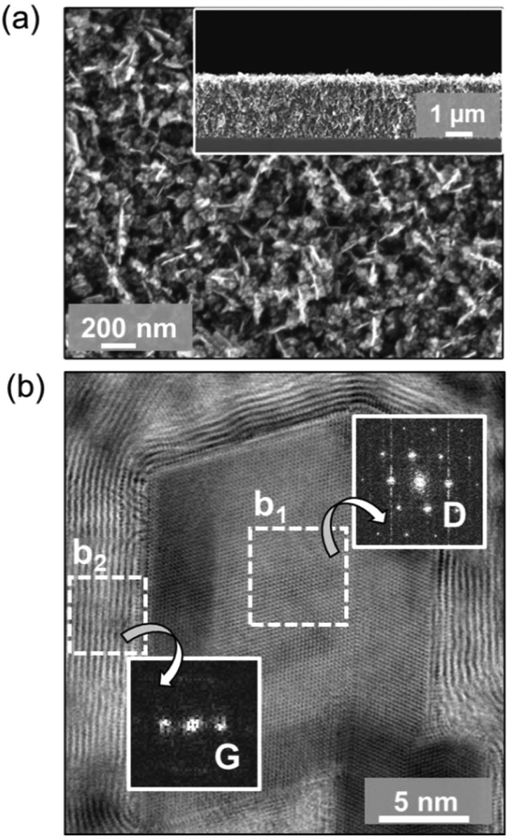 | ||
| Fig. 1 (a) SEM image of graphite@diamond nano-needles along with the cross-sectional SEM image shown in the inset. (b) Cross-sectional high resolution HAABF-STEM image of graphite@diamond nano-needles with the FT patterns displayed in the insets of (b), revealing the crystalline nature of diamond (D) in region b1 and graphite (G) in region b2. | ||
To illustrate more clearly the elemental distribution of the N-NCD film, spatially resolved STEM – electron energy loss spectroscopy (EELS) mapping was performed. A core-loss EELS spectrum scanned using a fine probe is shown in Fig. 2a, where diamond and graphite are seen in each point. Further fitting all collected spectra to references for graphite and diamond led to the generation of polymorph weight maps. Such a STEM–EELS mapping of the same region depicted in Fig. 2a is shown in Fig. 2b where diamond is in red and graphite is in green. Two summed selective area EELS spectra from the diamond and the graphite regions in Fig. 2b are then plotted in Fig. 2c. The carbon K-edge spectrum acquired from the diamond region (spectrum I) is typical of sp3-carbon, with a strong σ* contribution at 292 eV and a deep valley at 302.0 eV.40 In addition, the presence of graphite (spectrum II) is confirmed through the presence of a core-loss feature in the carbon-K edge at 285 eV (π* band).41–43 These STEM–EELS results together with the elemental maps confirm again the existence of diamond and graphite in a core–shell structure, in agreement with the Raman data (Fig. S1a†).
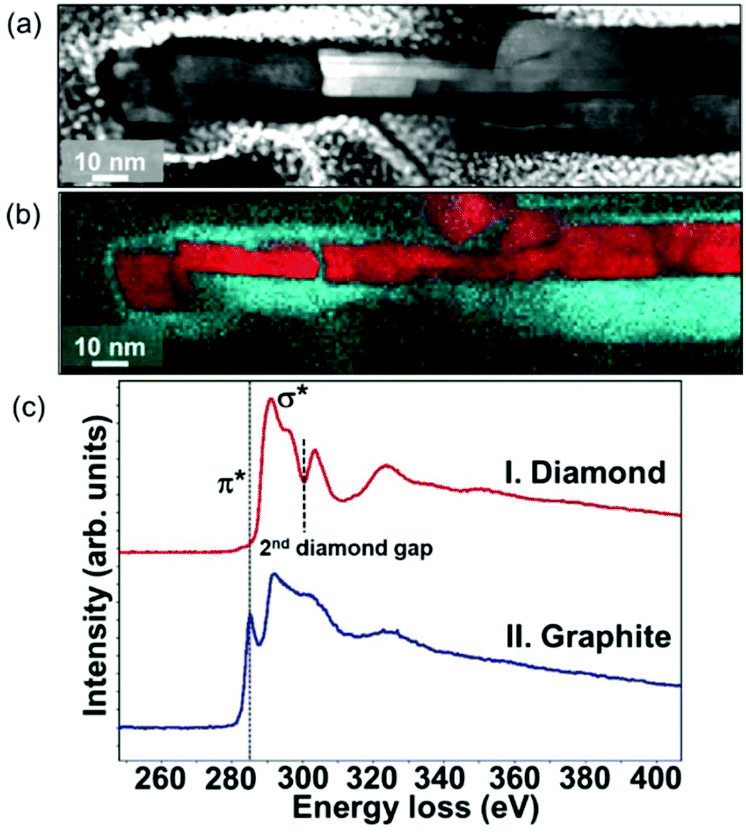 | ||
| Fig. 2 (a) HAABF-STEM micrograph of graphite@diamond nano-needles together with (b) composed EELS polymorph mapping for diamond (red) and graphite (blue). (c) Integrated EELS core-loss spectra taken from diamond and graphite regions in (b). | ||
To clarify the growth mechanism of graphite@diamond nanoneedles, the plasma constituents during the growth of graphite@diamond nanoneedles were further measured using in situ optical emission spectroscopy (OES) (Fig. S1b†). The peaks that represent the Balmer atomic hydrogen emission lines, the C2 swan system, the N2 peak, and the CN violet system are seen. Theoretically, it is known that the definite faces (e.g., (100) faces) of the nanodiamond clusters are preferentially attached to the CN species and trigger the formation of diamond nanoneedles. In other words, the growth of graphite@diamond nanoneedles originates in the CN species. However, a high substrate temperature is necessary for triggering the CN species in the induction of the attachment of C2 species through the CN adhered surface. For example, when the substrate temperature is 780 °C, CN species are dominant than CH species. The preferential attachment of C2 species and induced anisotropic growth of diamond grains occur consequently. The smaller grains inside graphite@diamond nanoneedles combine along any desired direction, ensuing in high aspect ratio diamond nanoneedles. Moreover, during the anisotropic growth, the surface C atoms surrounding the sp3-bonded diamond core tend to form sp2-bonded carbon as it is energetically favorable. That is, there is a natural tendency to form graphitic layers surrounding the anisotropic growth of diamond grains, namely a structure of graphite@diamond nanoneedles.
Performance of diamond supercabatteries
These graphite@diamond nano-needles are attempted to be employed as the capacitor electrode to construct diamond supercabatteries. Their capacitive behavior was first investigated in both aqueous and organic solutions using a three-electrode system. Due to the presence of the graphitic shell and rich surface functional groups, a relatively narrow potential window has been applied in this work. Fig. 3a illustrates their cyclic voltammograms (CVs) recorded in 1.0 M Na2SO4 at different scan rates within a potential window of 0–0.8 V. At all scan rates the CVs exhibit a symmetrical rectangular shape, indicating the ideal capacitive behavior of these N-NCD films. The estimated capacitance is 0.126, 0.131, 0.140, and 0.147 mF cm−2 at a scan rate of 100, 50, 20, and 10 mV s−1, respectively. The corresponding galvanostatic charge/discharge (GCD) curves are presented in Fig. 3b, where linear characteristics are seen in both charge and discharge sections. By applying different current densities ranging from 0.05, 0.02, 0.01, to 0.005 mA cm−2, the capacitance is calculated to be 0.115, 0.121, 0.128, and 0.135 mF cm−2, respectively. Compared to the capacitance of a BDD film (3.6–7 μF cm−2)18 and a N-doped ultrananocrystalline diamond film (17 μF cm−2),27 the capacitance of graphite@diamond nano-needles has been improved tens of times. The reason behind this is ascribed to their unique needle-like structure and the existence of nanographitic phases. The needle-like morphology leads to an enlarged surface area, while the presence of nanographitic phases (namely sp2-bonded carbon atoms) results in the improved electrical properties of these films, eventually leading to their much-enhanced capacitance.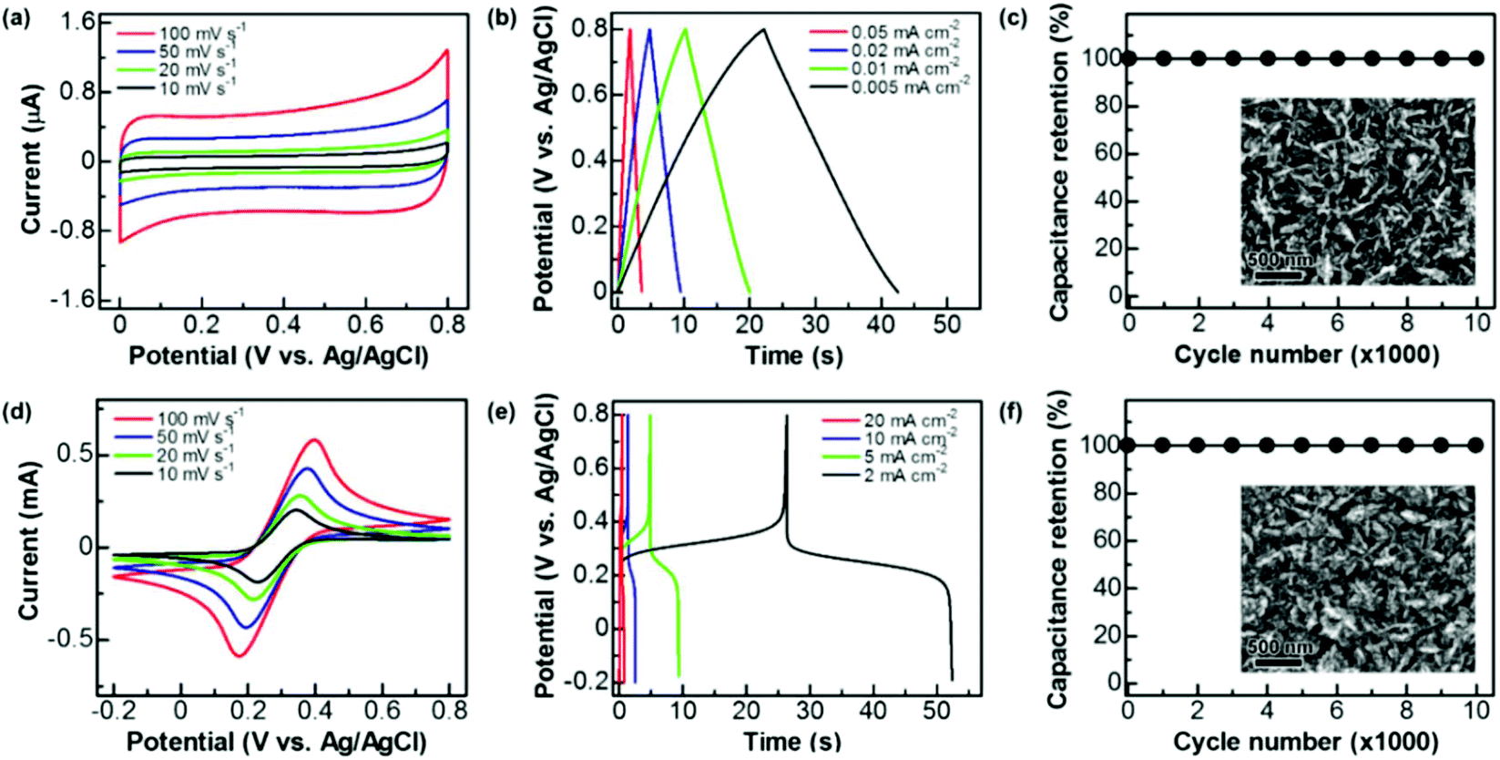 | ||
| Fig. 3 Capacitive performance of graphite@diamond nano-needles in 1.0 M Na2SO4 (a, b, c) and 1.0 M Na2SO4 + 0.05 M Fe(CN)63−/4− (d, e, f): (a, d) CVs at different scan rates, (b, e) GCD curves at different current densities, and (c, f) capacitance retention at the charge/discharge current densities of 0.02 mA cm−2 and 10 mA cm−2 in the solutions of 1.0 M Na2SO4 (c) and 1.0 M Na2SO4 + 0.05 M Fe(CN)63−/4− (f), respectively. The inset shows the SEM images of used graphite@diamond nano-needles after 10000 charge/discharge cycles. | ||
The capacitive behavior of these graphite@diamond nano-needles in organic solutions (here 0.1 M tetrabutylammonium tetrafluoroborate in propylene carbonate) was also investigated. The recorded CVs (Fig. S2a†) show a rectangular shape at all scan rates. The calculated capacitances are 0.06, 0.067, 0.075, and 0.084 mF cm−2 at the scan rates of 100, 50, 20, and 10 mV s−1, respectively. The obtained GCD curves at different current densities (Fig. S2b†) are symmetrical and linear in charge and discharge cycles, a typical characteristic of an ideal capacitor electrode. The estimated capacitances are 0.061, 0.067, 0.071, and 0.075 mF cm−2 at the current densities of 0.05, 0.02, 0.01, and 0.005 mA cm−2, respectively. Note here that the acquired capacitance of these graphite@diamond nano-needles is lower in this organic electrolyte than that in aqueous solutions, probably due to the relatively low conductivity and higher viscosity of organic solutions compared to aqueous ones,44,45 larger-sized ions in organic solutions, as well as the surface chemistry of used electrodes. The post-treatment of these films in a mixture of H2SO4 and HNO3 (v/v = 3:1) leads to an increase of the oxygen content,19i.e. the oxygen functional groups. These oxygen groups exhibit different electrochemical and capacitive activities in different electrolytes, resulting in varied capacitances of used electrodes in aqueous and organic solutions. The capacitance stability of these graphite@diamond nano-needles was further tested using the GCD technique in both aqueous and organic solutions. The applied current density was 0.02 mA cm−2 and the charge/discharge cycle number was 10000. As shown in Fig. 3c and Fig. S2c,† the initial capacitance remains unchanged after 10000 cycles in both solutions. The SEM images of the surface of used graphite@diamond nano-needles after this lifetime test are shown in the inset of Fig. 3c and Fig. S2c.† Compared to the as-grown graphite@diamond nano-needles (Fig. 1a), almost no surface damage or differences are observed. Such phenomena indicate the excellent capacitance stability of these graphite@diamond nano-needles, mainly due to the existence of diamond and the synergistic effect between diamond and graphite.
As mentioned, the (pseudo)capacitance of a capacitor electrode can be 100–1000 times enhanced once the redox electrolyte is applied.19,35–37 Therefore, the capacitance of graphite@diamond nano-needles in the redox-active electrolyte (here 0.05 M Fe(CN)63−/4− + 1 M Na2SO4) was measured using cyclic voltammetry and the GCD technique. All CVs (Fig. 3d) recorded at different scan rates within a potential window of −0.2–0.8 V show a well-defined pair of redox waves, obviously corresponding to the redox reaction of [Fe(CN)6]3− + e− ↔ [Fe(CN)6]4−. This fast and reversible faradaic reaction brings an additional pseudo-capacitance, which is much larger than the electrical double layer capacitance. At each scan rate, the absolute values of anodic and cathodic peak currents are almost equivalent. These currents are linearly increased with an increase of the scan rates, as expected for a pseudocapacitor electrode.5,6 The evaluated capacitances are 23.45, 33.64, 53.53, and 66.65 mF cm−2 at scan rates of 100, 50, 20, and 10 mV s−1, respectively. Meanwhile, the GCD curves were recorded at different current densities. The plateaus observed in all GCD curves (Fig. 3e) prove the involvement of redox reactions of Fe(CN)63−/4− during the charge/discharge processes. At each current density, the required times are almost identical for the charge and discharge processes. For instance, at a low current density of 2 mA cm−2, the coulombic efficiency is estimated to be about 98.75%. The calculated capacitances are 7.0, 12.8, 23.81, and 53.34 mF cm−2 at the current densities of 20, 10, 5, and 2 mA cm−2, respectively. As expected, these pseudocapacitances, originating from the rapid faradaic reactions of Fe(CN)63−/4− at the N-NCD film and the electrical double layer capacitances of the diamond film, are two orders of magnitude higher compared to those of graphite@diamond nano-needles in 1.0 M Na2SO4 aqueous solution. The cycling stability of the PC was also examined by the GCD technique at a current density of 10 mA cm−2. The variation of the pseudocapacitance is plotted as a function of the cycle number (Fig. 3f). After 10000 cycles no loss of the initial capacitance is observed, proving 100% capacitance retention. This is due to the stable faradaic process of Fe(CN)63−/4− at the N-NCD film as well as the high stability of graphite@diamond nano-needles under these conditions, as confirmed from its SEM image after such a lifetime test (the inset of Fig. 3f).
These capacitances are further compared with those reported when other types of diamond films, diamond nanostructures (fabricated using top-down, bottom-up, and template-free approaches),46,47 and diamond hybrids/composites16,48 are employed as the capacitor electrodes (Fig. S3†). These reported capacitances are in the range of 0.1–10 mF cm−2.49 The capacitance (0.147 mF cm−2) of graphite@diamond nano-needles in aqueous solutions falls in this domain. Upon further introduction of redox-active species in the electrolyte, their pseudocapacitance is found to be as high as 66.65 mF cm−2, a few times larger than those of most diamond pseudocapacitors.18,50
To explore the practical applications of graphite@diamond nano-needles for the construction of diamond supercabatteries, a two-electrode symmetrical supercapacitor device was assembled using two graphite@diamond films as the capacitor electrodes. For these tests, only aqueous solutions were used. Related CVs (Fig. 4a) and GCD curves (Fig. 4b) were first recorded in 1.0 M Na2SO4 solution by applying a cell voltage of 0.8 V. Similar to those obtained using a three-electrode system, the CVs at all scan rates are nearly rectangular and the GCD curves at different current densities are symmetrical and linear. These results confirm the ideal capacitive behavior of such an EDLC device. The capacitances estimated from CVs are 0.095, 0.103, 0.115, and 0.122 mF cm−2 at the scan rates of 100, 50, 20, and 10 mV s−1, respectively. The capacitances calculated from GCD curves are 0.089, 0.098, 0.108, and 0.12 mF cm−2 at the current densities of 0.05, 0.02, 0.01, and 0.005 mA cm−2, respectively.
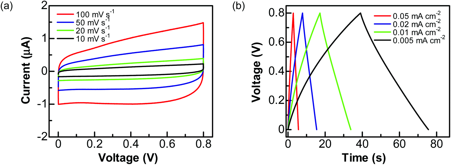 | ||
| Fig. 4 Capacitance performance of a graphite@diamond EDLC device in aqueous solution of 1.0 M Na2SO4: (a) CVs obtained at the scan rates of 100, 50, 20, and 10 mV s−1 and (b) GCD curves at different current densities of 0.05, 0.02, 0.01, and 0.005 mA cm−2. | ||
Then, a solution of 1 M Na2SO4 containing 0.05 M Fe(CN)63−/4− was used as the electrolyte. The performance of this PC device was studied by applying a cell voltage of 1 V. In the related CVs (Fig. 5a), a pair of redox peaks caused by the redox reactions of Fe(CN)63−/4− is seen at all scan rates. Here the peak potentials are different from those obtained using a three-electrode system, due to the varied configuration of electrode systems. The calculated pseudocapacitances are 11.92, 16.87, 24.53, and 28.82 mF cm−2 at the scan rates of 100, 50, 20, and 10 mV s−1, respectively. On the other hand, the GCD curves (Fig. 5b) show plateaus in the charge and discharge parts corresponding to the redox reactions of Fe(CN)63−/4−. The charges transferred in the charge and discharge processes are nearly the same. The estimated capacitances are 4.48, 8.07, 13.10, 27.62, and 60.26 mF cm−2 at the current densities of 20, 10, 5, 2 and 1 mA cm−2, respectively.
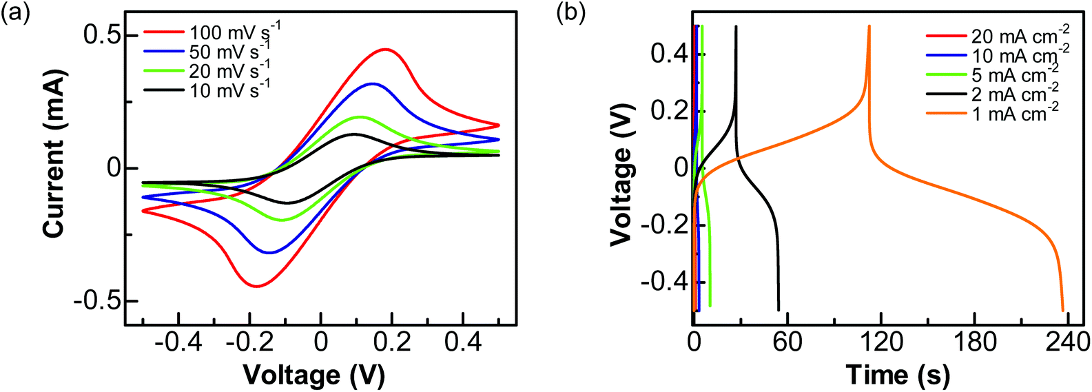 | ||
| Fig. 5 Capacitance performance of a graphite@diamond PC device in aqueous solution of 1.0 M Na2SO4 + 0.05 M Fe(CN)63−/4−: (a) CVs at the scan rates of 100, 50, 20, and 10 mV s−1 and (b) GCD curves at the current densities 20, 10, 5, 2, and 1 mA cm−2. | ||
To evaluate the overall performance of these diamond supercabatteries, their energy and power densities were further calculated based on the results acquired using the GCD technique.17,19,51,52 Six capacitor electrodes have been employed. The related Ragone plots (Fig. S4†) show that the EDLC device has a maximal energy density (E) of 0.013 W h kg−1 together with a maximal power density (P) of 12.79 W kg−1. These values are comparable with those of other diamond EDLC devices (E = 0.016 W h kg−1 and P = 9.54 W kg−1 with a larger applied cell voltage of 2.4 V (ref. 17)). The values of E and P of an EDLC device are expected to be further enhanced simply through the enlargement of cell voltage and/or using different electrolytes (e.g., ionic liquids).
Regarding the PC devices using six capacitor electrodes, their maximal E and P reach 10.40 W h kg−1 and 6.96 kW kg−1, respectively (Fig. S4†). Compared with those of N-NCD EDLC devices, they are enhanced about 800 and 230 times, respectively. Fig. 6 compares the obtained E and P for different diamond supercapacitors, including EDLCs and PCs constructed using BDD, the BDD network, and carbon nanofiber coated BDD.49 The E and P values of the as-fabricated PC device in this study are approximately similar to the values of diamond EC devices. Note here that the energy and power densities of the as-fabricated N-NCD supercabattery device are lower than those using BDD based capacitor electrodes. This is mainly due to the fact that the applied cell voltage (e.g., 1.0 V) for the current N-NCD supercabattery device is smaller than that (e.g., 2.4 V) has been applied for BDD based pseudocapacitor devices. Higher energy and power densities are expected for N-NCD supercabattery devices once cell voltages larger than 1.0 V are applied, the improved crystallinity and enlarged sp2-graphite-to-sp3-diamond ratios inside such graphite@diamond nano-needles are used, multi-electron transferred redox species in aqueous solution are introduced and an ionic or an organic redox electrolyte is employed. However, when compared to other energy storage devices (e.g., electrochemical capacitors, and batteries), this PC device still exhibits not only high P but also high E. Both values are larger than those of some reported supercapacitors and some batteries.
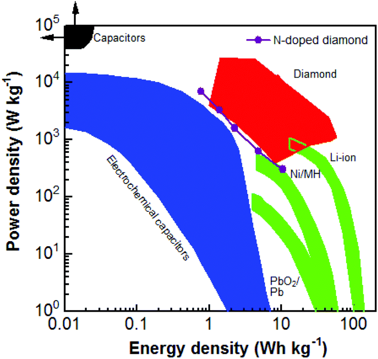 | ||
| Fig. 6 Ragone plot of the diamond supercabattery device in comparison with those of other diamond electrochemical capacitor devices, traditional capacitors, electrochemical capacitors, and batteries.49 Reproduced with permission.49 Copyright 2018, University of Siegen, Siegen, Germany. | ||
For practical applications, one stand-alone demonstrator (Fig. S5a†) has been designed to light a LED with a working voltage of 1.8 V. The related electrical circuit diagram consists of one or several devices assembled in series, one microcontroller to control the relays (switches) in the circuit and thus the charge and discharge processes of the devices and one LED. The working procedure was the same as the one reported (Fig. S5b†).19 Switch-1 (relay-1) is first connected until the devices are charged to a desirable voltage (here 3.0 V). Further open of switch-1 (relay-1) and subsequently the close of switch-2 (relay-2) result in the discharging process of the devices, leading to the illumination of the LED. Once the voltage of the devices decreases to a set value (here 1.6 V), switch-2 opens and switch-1 closes. Namely, a new charge/discharge cycle starts. The devices using scaled-up N-NCD films as capacitor electrodes were capable of illuminating this red LED for ten of seconds with a charging time of few seconds. Such a process was proved to be highly stable and reproducible. Therefore, diamond supercabatteries feature rapid charging possibility and slow discharging rates as well as good cycle ability, besides their high power and energy densities.
Conclusions
In conclusion, diamond supercabatteries are fabricated using the capacitor electrode of graphite@diamond nano-needles and aqueous redox electrolytes. Besides excellent stability and reversibility, they feature both high power and energy densities (e.g., an energy of 10.40 W h kg−1 together with a power density of 6.96 kW kg−1). To further improve the performance of these diamond supercabatteries, the applications of high cell voltages and/or different electrolytes (e.g., ionic liquids) are potential options. The post-treatment of graphite@diamond nano-needles to vary their crystallinity and sp2-graphite-to-sp3-diamond ratios will be helpful. The combination of graphite@diamond nano-needles with other functional or pseudocapacitive materials (e.g., metal oxide, conducting polymer, and carbon nanofiber) is also worth testing. Moreover, ultra-rapid charging of these diamond supercabatteries together with their slow charging processes is possible. Furthermore, with the rapid development of CVD growth technologies for the production of synthetic diamond films, the commercial price of diamond films decreases dramatically. High quality diamond can be fabricated with higher yield and lower price. Therefore, these diamond supercabatteries are eventually economically reasonable and will hold promise for both industrial and high-end applications, especially for those where both high power and energy densities are needed (e.g., uninterruptible power supply, regenerative braking systems for trains and electric vehicles, and replacement of charge stations to charge rapidly electric vehicles).Experimental section
Diamond films
The N-NCD films (namely graphite@diamond nano-needles) were grown on seeded n-type silicon (100) substrates (with a colloidal suspension of 5 nm detonation nanodiamonds)53 on an ASTeX 6500 series MWPECVD system. The growth conditions were as follows: a gas mixture of CH4 (45 sccm) + H2 (246 sccm) + N2 (9 sccm) (CH4/H2/N2 = 15/82/3), a microwave power of 3000 W, a total pressure of 65 Torr in the chamber, and a substrate temperature of around 780 °C. Before electrochemical measurements, the N-NCD films were immersed in a mixture of H2SO4 and HNO3 (v/v = 3:1) for 30 min, followed by cleaning with deionized water and drying under a N2 atmosphere.
Instrument
The surface and cross-sectional morphologies as well as the crystalline quality of the N-NCD films were characterized using field emission scanning electron microscopy (FESEM, Zeiss Ultra55, Germany) and visible-Raman spectroscopy (Horiba Jobin–Yvon T64000 spectrometer with λ = 488.0 nm). The microstructure of the N-NCD films was analyzed using a FEI Titan “cubed” microscope operating at 300 kV for HAABF-STEM. The convergence semi-angle ‘α’ used was 22 mrad, the inner acceptance semi-angle ‘β’ for HAABF-STEM imaging was 22 mrad, and the electron energy loss spectroscopy (EELS) collection angle used was also 22 mrad. The focused ion beam technique was used to prepare the STEM specimens of these samples. The plasma constituents during the growth of N-NCD films were recorded using in situ optical emission spectroscopy (OES, AvaSpec-2048 (Avantes). Electrochemical measurements were carried out on a CHI660E Potentiostat/Galvanostat (Shanghai Chenhua Inc., China). A standard three-electrode configuration was first employed to evaluate the electrochemical performance of the N-NCD films. In the three-electrode system, the N-NCD film was applied as the working electrode, an Ag/AgCl (3 M KCl) electrode was used as the reference electrode and a coiled Pt wire was used as the counter electrode. The supercapacitor devices were assembled using a two-electrode symmetrical system, where two N-NCD films were served as the capacitor electrodes and a Nafion® film (Alfa Aesar) with a thickness of 50 μm as the separator. The effective area of an N-NCD capacitor electrode that was exposed to the electrolyte was about 0.05 cm2. An aqueous solution of 1.0 M Na2SO4 and an organic solution of 0.1 M tetrabutylammonium tetrafluoroborate (TBABF4) in propylene carbonate were used for the N-NCD EDLCs, while a redox-active electrolyte of 1.0 M Na2SO4 containing 0.05 M K3Fe(CN)6/K4Fe(CN)6 was employed for the construction of the N-NCD PCs. Cyclic voltammograms (CVs) were obtained at different scan rates. The galvanostatic charge/discharge (GCD) curves were recorded at different current densities.Conflicts of interest
There are no conflicts to declare.Acknowledgements
S. Yu and K. J. Sankaran contributed equally to this work. N. Yang acknowledges funding from the German Science Foundation under the project of YA344/1-1. J. Verbeeck and S. Korneychuk acknowledge the funding from the GOA project “Solarpaint” of the University of Antwerp. The Qu-Ant-EM microscope was partly funded by the Hercules fund from the Flemish Government. K. J. Sankaran and K. Haenen like to acknowledge the financial support of the Methusalem “NANO” network. S. Yu likes to acknowledge the financial support from fundamental research funds for the central universities (Grant No. SWU019001).Notes and references
- P. Simon, Y. Gogotsi and B. Dunn, Science, 2014, 343, 1210–1211 CrossRef CAS PubMed.
- C. Zhong, Y. Deng, W. Hu, J. Qiao, L. Zhang and J. Zhang, Chem. Soc. Rev., 2015, 44, 7484–7539 RSC.
- F. Béguin, V. Presser, A. Balducci and E. Frackowiak, Adv. Mater., 2014, 26, 2219–2251 CrossRef PubMed.
- G. Wang, L. Zhang and J. Zhang, Chem. Soc. Rev., 2012, 41, 797–828 RSC.
- T. Brousse, D. Bélanger and J. W. Long, J. Electrochem. Soc., 2015, 162, A5185–A5189 CrossRef CAS.
- I. Aldama, V. Barranco, J. Ibañez, J. M. Amarilla and J. M. Rojo, J. Electrochem. Soc., 2018, 165, A4034–A4040 CrossRef CAS.
- W. Zuo, R. Li, C. Zhou, Y. Li, J. Xia and J. Liu, Adv. Sci., 2017, 4, 1600539 CrossRef PubMed.
- C. Costentin, T. R. Porter and J.-M. Savéant, ACS Appl. Mater. Interfaces, 2017, 9, 8649–8658 CrossRef CAS PubMed.
- N. Yang, S. Yu, J. V. Macpherson, Y. Einaga, H. Zhao, G. Zhao, G. M. Swain and X. Jiang, Chem. Soc. Rev., 2019, 48, 157–204 RSC.
- N. Yang, J. S. Foord and X. Jiang, Carbon, 2016, 99, 90–110 CrossRef CAS.
- K. Siuzdak and R. Bogdanowicz, Energy Technol., 2018, 6, 223–237 CrossRef CAS.
- E. Tamburri and M. L. Terranova, in Advanced Electrode Materials, ed. A. Tiwari, F. Kuralay and L. Uzun, co-published by John Wiley & Sons, Inc. Hoboken, New Jersey, and Scrivener Publishing LLC, Beverly, Massachusetts, 2017, pp. 27–60 Search PubMed.
- L. G. Wang and A. Zunger, Phys. Rev. B: Condens. Matter Mater. Phys., 2002, 66, 161202 CrossRef.
- F. Gao and C. E. Nebel, ACS Appl. Mater. Interfaces, 2016, 8, 28244–28254 CrossRef CAS PubMed.
- K. Honda, T. N. Rao, D. A. Tryk, A. Fujishima, M. Watanabe, K. Yasui and H. Masuda, J. Electrochem. Soc., 2001, 148, A668–A679 CrossRef CAS.
- E. C. Almeida, M. R. Baldan, J. M. Rosolen and N. G. Ferreira, Diamond Relat. Mater., 2008, 17, 1529–1533 CrossRef CAS.
- S. Yu, N. Yang, H. Zhuang, S. Mandal, O. A. Williams, B. Yang, N. Huang and X. Jiang, J. Mater. Chem. A, 2017, 5, 1778–1785 RSC.
- S. Yu, N. Yang, H. Zhuang, J. Meyer, S. Mandal, O. A. Williams, I. Lilge, H. Schönherr and X. Jiang, J. Phys. Chem. C, 2015, 119, 18918–18926 CrossRef CAS.
- S. Yu, N. Yang, M. Vogel, S. Mandal, O. A. Williams, S. Jiang, H. Schönherr, B. Yang and X. Jiang, Adv. Energy Mater., 2018, 8, 1702947 CrossRef.
- S. Bhattacharyya, O. Auciello, J. Birrell, J. A. Carlisle, L. A. Curtiss, A. N. Goyette, D. M. Gruen, A. R. Krauss, J. Schlueter, A. Sumant and P. Zapol, Appl. Phys. Lett., 2001, 79, 1441–1443 CrossRef CAS.
- C.-R. Lin, W.-H. Liao, D.-H. Wei, J.-S. Tsai, C.-K. Chang and W.-C. Fang, Diamond Relat. Mater., 2011, 20, 380–384 CrossRef CAS.
- Y. Liu, S. Chen, X. Quan, X. Fan, H. Zhao, Q. Zhao and H. Yu, Appl. Catal., B, 2014, 154–155, 206–212 CrossRef CAS.
- G. Bhattacharya, K. J. Sankaran, S. B. Srivastava, J. P. Thomas, S. Deshmukh, P. Pobedinskas, S. P. Singh, K. T. Leung, M. K. Van Bael, K. Haenen and S. S. Roy, Electrochim. Acta, 2017, 246, 68–74 CrossRef CAS.
- J. Shalini, K. J. Sankaran, C.-L. Dong, C.-Y. Lee, N.-H. Tai and I. N. Lin, Nanoscale, 2013, 5, 1159–1167 RSC.
- S. A. Skoog, P. R. Miller, R. D. Boehm, A. V. Sumant, R. Polsky and R. J. Narayan, Diamond Relat. Mater., 2015, 54, 39–46 CrossRef CAS.
- S. Raina, W. P. Kang and J. L. Davidson, Diamond Relat. Mater., 2009, 18, 574–577 CrossRef CAS.
- W. Tong, K. Fox, A. Zamani, A. M. Turnley, K. Ganesan, A. Ahnood, R. Cicione, H. Meffin, S. Prawer, A. Stacey and D. J. Garrett, Biomaterials, 2016, 104, 32–42 CrossRef CAS PubMed.
- R. Torz-Piotrowska, A. Wrzyszczyński, K. Paprocki and E. Staryga, Opt. Mater., 2009, 31, 1870–1872 CrossRef CAS.
- S.-S. Yan, H.-Y. Peng, Z.-B. Zhao, M.-M. Pan, D.-L. Yang, J.-H. A, G.-L. Ye, C.-T. Wang and X.-W. Guo, J. Inorg. Mater., 2018, 33, 565–569 CrossRef.
- Q. Zhang, Y. Liu, S. Chen, X. Quan and H. Yu, J. Hazard. Mater., 2014, 265, 185–190 CrossRef CAS PubMed.
- J. Zhang and L. Dai, ACS Catal., 2015, 5, 7244–7253 CrossRef CAS.
- K. J. Sankaran, N. H. Tai and I. N. Lin, J. Appl. Phys., 2015, 117, 075303 CrossRef.
- K. J. Sankaran, J. Kurian, H. C. Chen, C. L. Dong, C. Y. Lee, N. H. Tai and I. N. Lin, J. Phys. D: Appl. Phys., 2012, 45, 365303 CrossRef.
- D. J. Garrett, K. Ganesan, A. Stacey, K. Fox, H. Meffin and S. Prawer, J. Neural Eng., 2012, 9, 016002 CrossRef PubMed.
- S.-E. Chun, B. Evanko, X. Wang, D. Vonlanthen, X. Ji, G. D. Stucky and S. W. Boettcher, Nat. Commun., 2015, 6, 7818 CrossRef CAS PubMed.
- L.-Q. Mai, A. Minhas-Khan, X. Tian, K. M. Hercule, Y.-L. Zhao, X. Lin and X. Xu, Nat. Commun., 2013, 4, 2923 CrossRef.
- D. Vonlanthen, P. Lazarev, K. A. See, F. Wudl and A. J. Heeger, Adv. Mater., 2014, 26, 5095–5100 CrossRef CAS PubMed.
- A. C. Ferrari, J. C. Meyer, V. Scardaci, C. Casiraghi, M. Lazzeri, F. Mauri, S. Piscanec, D. Jiang, K. S. Novoselov, S. Roth and A. K. Geim, Phys. Rev. Lett., 2006, 97, 187401 CrossRef CAS PubMed.
- G. Kalita, K. Wakita and M. Umeno, RSC Adv., 2012, 2, 2815–2820 RSC.
- P. Kovarik, E. B. D. Bourdon and R. H. Prince, Phys. Rev. B: Condens. Matter Mater. Phys., 1993, 48, 12123 CrossRef CAS PubMed.
- S. Prawer, J. L. Peng, J. O. Orwa, J. C. Mccallum, D. N. Jamieson and L. A. Bursill, Phys. Rev. B: Condens. Matter Mater. Phys., 2000, 62, R16360–R16363 CrossRef CAS.
- S.-S. Chen, H.-C. Chen, W.-C. Wang, C.-Y. Lee, I.-N. Lin, J. Guo and C.-L. Chang, J. Appl. Phys., 2013, 113, 113704 CrossRef.
- J. Kurian, K. J. Sankaran, J. P. Thomas, N. H. Tai, H.-C. Chen and I. N. Lin, J. Phys. D: Appl. Phys., 2014, 47, 415303 CrossRef.
- J. Varghese, H. Wang and L. Pilon, J. Electrochem. Soc., 2011, 158, A1106–A1114 CrossRef CAS.
- F. Barzegar, D. Y. Momodu, O. O. Fashedemi, A. Bello, J. K. Dangbegnon and N. Manyala, RSC Adv., 2015, 5, 107482–107487 RSC.
- H. Zhuang, N. Yang, H. Fu, L. Zhang, C. Wang, N. Huang and X. Jiang, ACS Appl. Mater. Interfaces, 2015, 7, 5384–5390 CrossRef CAS PubMed.
- F. Gao, M. T. Wolfer and C. E. Nebel, Carbon, 2014, 80, 833–840 CrossRef CAS.
- H. Zanin, P. W. May, D. J. Fermin, D. Plana, S. M. C. Vieira, W. I. Milne and E. J. Corat, ACS Appl. Mater. Interfaces, 2014, 6, 990–995 CrossRef CAS PubMed.
- S. Yu, PhD thesis, University of Siegen, Germany, 2018.
- D. Aradilla, F. Gao, G. L. Malandrakis, W. Müller-Sebert, P. Gentile, M. Boniface, D. Aldakov, B. Iliev, T. J. S. Schubert, C. E. Nebel and G. M. Bidan, ACS Appl. Mater. Interfaces, 2016, 8, 18069–18077 CrossRef CAS PubMed.
- K. V. Sankar and R. Kalai Selvan, Carbon, 2015, 90, 260–273 CrossRef CAS.
- K. Sun, E. Feng, H. Peng, G. Ma, Y. Wu, H. Wang and Z. Lei, Electrochim. Acta, 2015, 158, 361–367 CrossRef CAS.
- O. A. Williams, O. Douhéret, M. Daenen, K. Haenen, E. Ōsawa and M. Takahashi, Chem. Phys. Lett., 2007, 445, 255–258 CrossRef CAS.
Footnotes |
| † Electronic supplementary information (ESI) available. See DOI: 10.1039/c9nr07037k |
| ‡ Equally contributed. |
| This journal is © The Royal Society of Chemistry 2019 |