
 Open Access Article
 This Open Access Article is licensed under a Creative Commons Attribution-Non Commercial 3.0 Unported Licence
Identification of vibration modes in single-molecule junctions by strong inelastic signals in noise†
Sumit
Tewari‡
 ,
Carlos
Sabater§
and
Jan
van Ruitenbeek
*
,
Carlos
Sabater§
and
Jan
van Ruitenbeek
*
Huygens-Kamerlingh Onnes Laboratory, Leiden University, Niels Bohrweg 2, 2333 CA Leiden, The Netherlands. E-mail: ruitenbeek@physics.leidenuniv.nl; Tel: +31 (0)71 527 5450
First published on 6th September 2019
Abstract
Conductance measurements in single-molecule junctions (SMJs) are on many occasions accompanied by inelastic spectroscopy and shot-noise measurements in order to obtain information about different vibration modes (or vibrons) and channels involved in the transport respectively. We have extended the single-molecule shot-noise measurements, which were previously performed at low bias, to high bias and we have studied the effects of these vibrons on the noise for a Deuterium (D2) molecule between Pt leads. We report here two important findings from these measurements. First, we find in our noise measurements that at the vibron energies of the molecule, a two-level fluctuation (TLF) is excited in the junction. Second, we show that in the presence of this TLF, a form of enhanced noise spectroscopy can be performed to detect inelastic electron–vibron interactions, by studying the third derivative of the noise (d3SI/dV3). This is possible because TLFs are insensitive to elastic scattering of electrons from defects, which nevertheless leave their signature in the usual inelastic electron tunnelling spectroscopy (IETS) measurements.
1. Introduction
Single molecule conductance measurements are possible now since nearly three decades. Soon after the first single molecule experiment,1 researchers started to explore the other degrees of freedom, for example, the effect of molecular vibrations2,3 on electronic transport and shot-noise measurements.4 The study of molecular vibrations using charge transport measurements helped to further strengthen the claim of contacting single molecules and the study of low-bias shot noise provides information about the number of channels involved in the charge transport.4,5 In this article, we will refer to a vibration mode of the molecule as a vibron and the vibrations in the bulk metallic lead as phonons.The vibration measurements done by studying charge transport through a single molecule depend strongly on the electron–vibron (e–vib) coupling strength, and on the effective on-site electron charging energy. For stronger coupling between electrons and vibrons, the electrons could have large transit times on the molecule and this could even polarize the molecule. This is seen as polaron formation and the transport in this regime is incoherent hopping transport.6,7 In the other limit, for weak electron–vibron coupling the traversal time for an electron to cross the molecule is much smaller than the oscillation period of the vibron modes of the molecule. On applying a bias V ≥ ħω/e across the molecule, where ħω is the energy of a vibron, the electrons crossing the molecule loose part of their energy to emit/excite a vibron of the molecule. This is visible in the differential conductance as a small step-change, at least for simple coherent off-resonant transmission and for weak electron–vibron coupling and weak electron–electron interaction strength.
The first measurements aimed at studying such electron–vibron interaction on single molecules2 were done for electrons crossing a single acetylene (C2H2) molecule absorbed on a Cu(100) surface. A step-up or increase in conductance at a voltage equal to ħω/e was recorded. This measurement was done in tunneling mode (with transmission, T ≪ 1) using a scanning tunneling microscope (STM) and the increase in conductance at energy ħω was attributed to the opening of a second inelastic channel. In another measurement done on a single H2 molecule attached between two Pt leads,8,9 a step-down or decrease in the molecular conductance was recorded. This measurement was done in point contact mode with transmission (T) close to unity. A similar decrease in conductance is also recorded in mono-atomic chains made of gold atoms,3,10 where the transport is again ballistic. For these contacts with high transmission (T ≈ 1), back-scattering of electrons due to lack of available empty states in the forward direction is considered to be the reason for the decrease in conductance. The crossover between the two transport regimes, from the low transmission (T ≪ 1) where the conductance shows a step-up to the high transmission regime (T ≈ 1) where the conductance shows a step-down has been observed in experiments.11–13 This crossover can be explained using a single vibron model in the weak electron–vibron coupling regime.7,14–16 These electron–vibron interactions are studied mostly using inelastic electron tunnelling spectroscopy (IETS), where the second derivative of the current (d2I/dV2) gives a peak at the position corresponding to the energy of the vibron. However, these steps are very small, around 1% of the conductance values, and could be very difficult to detect in the presence of conductance oscillations which occur due to elastic scattering of electrons through defects in the leads.17–19
In this article, we demonstrate the results obtained by combining a high-bias shot-noise measurements with the usual differential conductance at energies where a vibron in a D2 molecule between Pt leads is excited. We show the emergence of a non-white noise spectra close to the energies corresponding to the vibration energy of the molecule. We attribute this to excitation of two-level fluctuations (TLF) in the molecule. Such TLF have been reported previously in similar systems by Thijssen et al.20 We show here that one could perform an enhanced inelastic electronic noise spectroscopy by studying the third derivative of the measured high bias noise signal, d3SI/dV3 which may offer a new tool for identifying vibration excitation in molecular junctions.
2. Experimental setup
To study shot noise at energies where the vibration modes of the single molecules are present, one has to fight with the notorious 1/f noise which scales with the square of the applied bias voltage. We have developed recently21 a new high-bias shot-noise measurement setup which works in MHz regime and can be useful in studying such molecular systems. We have also demonstrated earlier using this setup shot-noise measurements up to 800 mV on single Au-atomic point contacts22 and have shown how the elastic and inelastic part of the transport can give highly non-linear shot noise, due to energy and voltage dependence of the transmission at such high bias. A graphical illustration of the setup and a schematic of the circuit diagram taken from Tewari et al.22 is shown in Fig. 1. The setup is mounted on a cryogenic dipstick in order to allow measurements at liquid He temperature. The gas molecules are deposited using a capillary tubing which goes all the way from a gas reservoir on the top to a break-junction sample mounted at the bottom. Noise measurements are done using a cross-correlation technique for which we have connected two cryogenic amplifiers in parallel at a short distance (approximately 1 cm) from the sample followed by two parallel room temperature amplifiers. For fast measurements of the noise, while still recording all the spectra at each applied bias voltage, we have incorporated a field programmable gate array (FPGA) in the spectrum analyzer. Conductance measurements are done by means of a lock-in amplifier using an input AC modulation signal of few mV amplitude over the sample and 677 Hz frequency. The details of the system and its benefits are discussed in our previous publication.21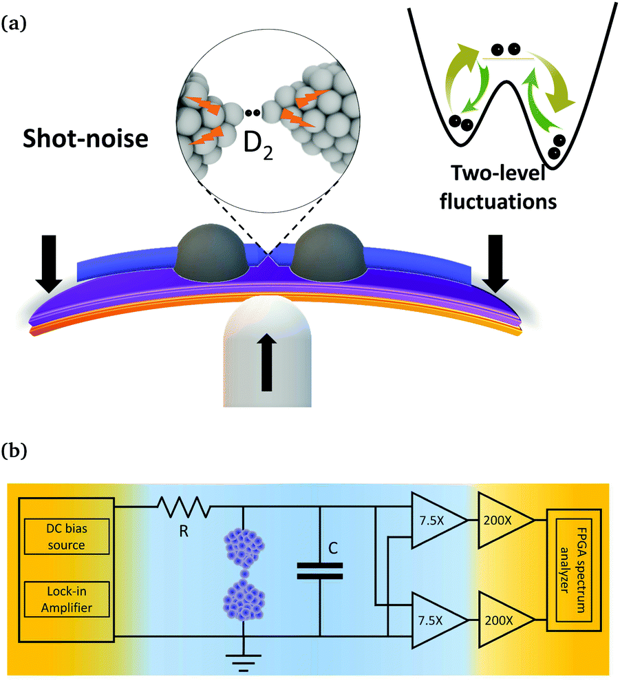 | ||
| Fig. 1 (a) Graphical illustration of the mechanically controlled break junction setup, including a representation of the TLF. (b) Schematic of the measurement circuit reproduced from Tewari et al.22 The color gradient shows qualitatively the operating temperature from 300 K (orange) to 4.2 K (blue). The setup consists of a cryogenic (7.5×) and room temperature amplifier (200×) together giving 1500 times amplification. The decoupling resistor R is 10 kohm and the total stray input capacitance at the cryo-amplifier is around 14 pF. | ||
3. Results and discussion
Single molecule measurements in general (not specific to our D2 molecule) are more likely to become affected by two-level fluctuations (TLF) than purely metallic atomic contacts. Such TLF are attributed to the switching between two (or more) conformational states with similar energy separated by a small barrier.20 These TLF can also occur in metallic point contacts and atomic chains. There they can be attributed to changes in position of a defect in the leads, close to the point contact. Materials like Pt show much stronger signals due to such TLF as compared to Au.21 Here, we have taken special care to avoid such TLF in the Pt leads by pre-annealing the break-junction notched wire in a separate UHV setup (10−9 mbar) for 3–4 hours at 300 °C. After this, we mounted carefully the sample back in the dipstick for pumping and cool down, avoiding introducing new strain in the notch. Such a pre-annealing step is essential as we don't want the noise coming from TLF of the leads to affect our molecule noise measurement.For clean deposition of the molecules, the capillary was baked before cool down at high vacuum (10−6 mbar) and several flushing cycles with clean D2 gas were done prior to breaking the Pt wire. For clean operation, the Pt wire is broken only when the system is cold and the sample is at cryogenic vacuum. Next, conductance and noise measurements of clean Pt were performed to check the cleanliness of the contact and also to train23 the junction prior to molecule deposition. Fig. 2 shows white noise spectra recorded on a clean Pt atomic contact up to 4.9 μA current (which is approximately 45 mV voltage drop over the 1.4 G0 junction resistance). This experiment shows the benefit of measuring shot noise at the MHz frequency range, as we don't have any detectable 1/f noise signal in our measurements. The spectra also confirm that there are no two-level fluctuations initiated in the clean Pt junctions.
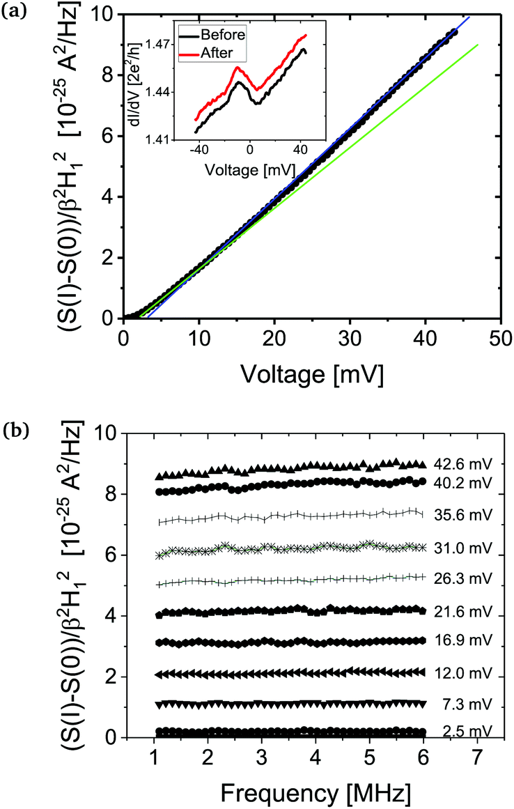 | ||
| Fig. 2 (a) Shot-noise measurements on a clean Pt atomic contact up to 44 mV bias, which for the zero bias conductance of the contact is equivalent to 4.9 μA current. The factor β2H12 corrects for the transfer characteristics of the measurement circuit, for details see Tewari et al.21 The inset shows the differential conductance of the contact taken before (black) and after (red) the shot-noise measurements. Two linear fits (blue and green) to the shot noise data cross at the phonon frequency of the Pt junction which is around 10 mV. (b) White noise spectra showing the absence of 1/f noise and two-level fluctuations, up to the highest applied bias. | ||
The procedure that we follow in our measurement is to perform differential conductance measurements of the junction two times: before and after the shot-noise measurement series. This helps in confirming the stability of the junction during the noise measurements. A kink or a linear deviation in the shot-noise data can be seen in Fig. 2 (a) which corresponds to the phonon frequency of the Pt junction which is around 10 mV. The rounding of the noise at the low bias (main panel, ≤2 mV) is due to submerging of the shot noise in the thermal noise background at the measurement temperature of 5 K.
While depositing the molecules, Pt conductance breaking traces are continuously monitored. It is known from previous conductance measurements for this system that a D2 molecule attached between Pt leads gives rise to a conductance plateau at 1 G0. Therefore, once we started seeing such 1 G0 plateau appearing, we stop the deposition. Once the D2 molecule is stable between the Pt leads, point contact spectroscopy or dI/dV measurements of such a junction are known to show a step-down or decrease of conductance due to inelastic interaction with the vibron of the molecule. This we also found in our experiments (see Fig. 3(a) and (c)) in agreement with the literature.4,8,9
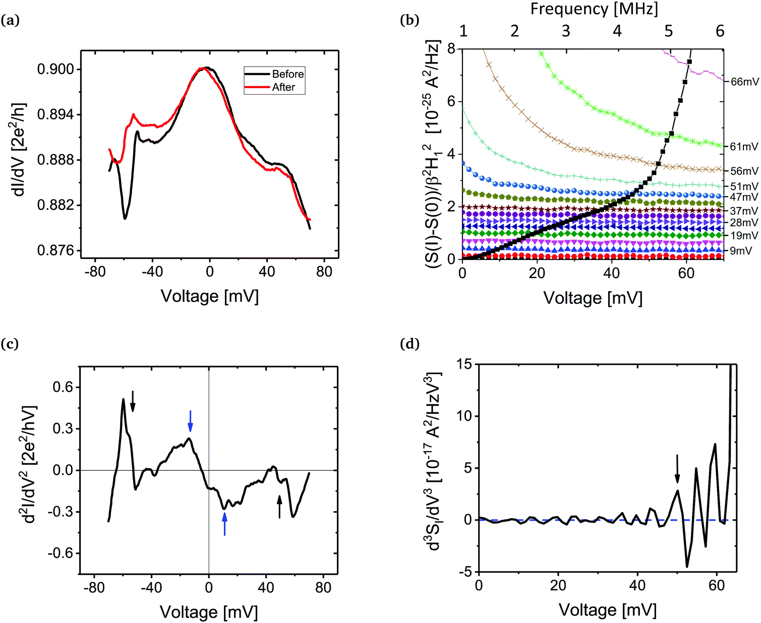 | ||
| Fig. 3 Junction 1: (a) differential conductance spectrum for a Pt–D2–Pt junction taken before (black) and after (red) the noise measurement, showing a step down at about 50 mV. The left shoulder of the dI/dV spectrum shows a signature of two-level fluctuations (peak) similar to Thijssen et al.20 (b) High-bias shot-noise measurements (black) taken up to 60 mV bias (i.e. 4.2 μA for G(0 V) = 0.9 G0). The noise spectra (in color and axis along the top) are shown from 1 to 6 MHz frequency. (c) Usual IETS spectrum of the junction showing the vibrational modes of the molecule (black arrows) and of the Pt leads (blue arrows). (d) The IENS-3 spectrum showing positions of inelastic interactions giving rise to two-level fluctuations in the molecule. The first peak marked with a black arrow, points towards a vibrational mode excitation of the molecule, while the other peaks correspond to inelastic interactions due to more complex atomic-scale dynamics occurring as the applied bias is increased further. | ||
Next, we perform high-bias shot noise measurements on this junction. In Fig. 3(b) we show the corresponding shot-noise measurement results. Initially, at low bias, the shot noise shows a linear increase (shown with black solid symbols) and then approximately at the point where a vibrational mode is excited shown by a step-down in the conductance (Fig. 3(a)), we see a non-linear increase in the noise. We repeated this measurement for different stretching states of the molecular junction, which changes the vibrational energy,4 and we found that the locations where the shot-noise starts to deviate from linearity also changes accordingly. The black data points in Fig. 3(b) are obtained as the average of the noise between 1 and 6 MHz. However, the same figure also shows the actual spectra, and demonstrates that the spectra are no longer white starting from the point of deviation from linearity in the black curve.
The detection of these non-white spectra suggests that another source of noise is activated, which we attribute to two-level fluctuations that are excited by the vibrons. In the absence of such spectral information, one would be tempted to attribute this non-linear increase in shot noise to a non-equilibrium increase in population24–27 of the vibrons due to their larger relaxation time. As shown in our earlier publication22 elastic scattering by defects could also add to the non-linearities in the shot noise. But, as our conductance values are not very close to 1 G0, we expect the contribution of such elastically scattered electrons to be small.
It is also possible that there are multiple two-level fluctuations excited by the vibrons resulting in 1/f noise spectra, but this we cannot confirm with our setup as we cannot measure the full spectra down to lower frequencies. However, excitation of a single TLF is more likely to be the case, as shown by Thijssen et al.20 and supported by the peak visible at the left shoulder in the dI/dV close to −50 mV, shown in Fig. 3(a).
3.1. Inelastic electron noise spectroscopy (IENS)
The noise recorded here for the first time at the vibration threshold of a single-molecule junction, demonstrates that the spectrum is not consistent with a process involving just inelastic scattering on a vibration mode. The spectrum is characteristic for excitation of a TLF, and the fact that this occurs at the threshold of the vibron excitation agrees with the model of vibrationally induced two-level fluctuations proposed by Thijssen et al.20 The fact that this signature of TLF is visible in noise, despite the fact that the differential conductance does not display clear evidence for TLF, suggests that the interaction with TLF may be widely present in molecular junctions. Here, we propose to turn this observation to our advantage.Use of shot noise as a tool for spectroscopy has been shown previously, under the name of inelastic electron noise spectroscopy (IENS).25 By studying inelastic interactions in Au atomic point contacts, linear deviations from the linear 2eIF relation for shot noise has been demonstrated. Here, we exploit vibrationally induced two-level fluctuations for detecting vibron energy thresholds. As the two-level fluctuations (TLFs) are fluctuations representing changes in the resistance, the signal increases as the square of the input current or the applied bias, and the d3SI/dV3 of the measured noise (SI) should show peaks corresponding to the TLF excited by inelastic interactions. We call this inelastic electron noise spectroscopy-3 (IENS-3). IENS-3 holds a unique benefit over the inelastic electron tunnelling spectroscopy (IETS), which is used widely to study electron–vibron interactions in single-molecules. This is because IENS-3 is sensitive to only the excitation of TLFs (which are vibron induced as shown in this manuscript), while on the contrary, the peaks in the IETS spectrum could have multiple origins. The details about how the third order derivative is extracted from the noise data are given in the ESI.†
We discuss here three different junctions and present also their IENS-3 spectra. More examples are provided in the ESI.†Fig. 3 shows a first example of the benefit of IENS-3 over IETS. Here, seeing the IETS spectrum (Fig. 3(c)) it is rather difficult to distinguish between peaks originating due to inelastic scattering and other structures appearing due to elastic quantum interference effects. We mark the most probable position for the energy of the vibron at around 60 mV. On the contrary, in the IENS-3 spectrum (Fig. 3(d)), the first peak (marked with an arrow) corresponds to the excitation of a TLF due to inelastic effects. This peak thus marks clearly the position of the vibration mode energy of the molecule and the spectrum is not affected by the background conductance fluctuations. As we keep increasing further the applied voltage bias, we may hit higher energy vibrons but it could also lead to a more complex atomic-scale dynamics due to an interaction between the excited TLF and the molecular vibrons. This can lead to the other peaks and structures shown in the IENS-3 spectrum, for which we cannot offer a straightforward interpretation at this stage.
Two more examples for comparison between IETS and IENS-3 structures are shown in Fig. 4. Here again one can see that IENS-3 shows clear peaks marking the position of inelastic interactions which excite TLF. Junction 2, Fig. 4, points towards a stretched state of the molecule which leads to higher energy vibration modes and lower conductance values.4 In this example the IETS signal (Fig. 4(b)) also has clear peaks pointing towards the position of the vibrons, which match well with that of the IENS-3 data (Fig. 4(c)). In the last example, for Junction 3, shown in Fig. 4(d–f), we note first that the differential conductance shows a step-up at energies close to the energy of the vibrons. This is something which has not been reported in experiments before, but such a possibility has already been discussed theoretically by Kristensen et al.28 A detailed discussion on this is given in the ESI† along with other experimental data-sets. However, important to note is that even in this example the IETS spectra (Fig. 4(e)) is heavily populated by multiple peaks, and it is difficult to pin-point the vibron energy. However, the IENS-3 signal does show a clear first peak occurring close to 50 mV.
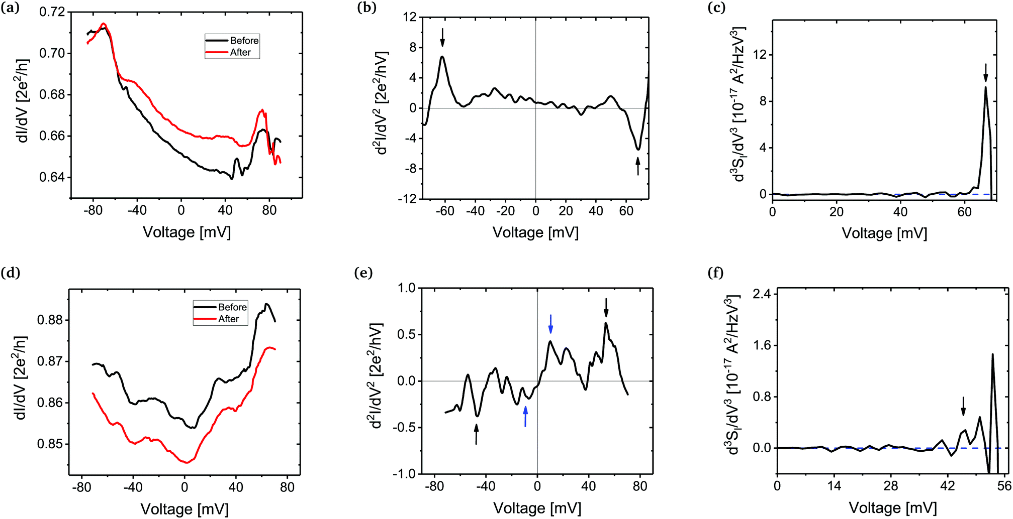 | ||
| Fig. 4 Junction 2: (a) differential conductance for a Pt–D2–Pt junction in a stretched state. (b) IETS spectrum of the junction showing two distinct peaks pointing towards the vibrational modes of the molecule (black arrows). (c) The IENS-3 spectrum showing enhanced peaks corresponding to the positions of inelastic interactions (black arrow). Here the noise measurement is performed for only positive bias. Junction 3: (d) differential conductance showing a step-up taken before (black) and after (red) the noise measurement. This is similar to a step up case discussed in Kristensen et al.28 (e) Usual IETS spectrum of the junction showing weak detection of the vibrational modes of the junction (black arrows). (f) The IENS-3 spectrum showing enhanced peak corresponding to the positions of inelastic interactions (black arrow). Here the noise measurement is performed for only positive bias. | ||
IENS-3 will detect only those inelastic interactions which lead to two-level fluctuations. This probably explains why in Junction 1 and 3 the IETS spectrum shows the position of the vibration mode of the Pt metallic leads at a low bias of around 10 mV, while there is no signature in the corresponding IENS-3 spectrum. This also confirms that by doing the pre-annealing we were able to successfully reduce defects in the Pt leads which could otherwise give rise to TLF in the leads.
We note that, for the results presented here almost none of the examples show clear signatures of two-level fluctuations visible in the differential conductance measurements, in the form of peaks in dI/dV. The timescales of the TLFs involved are expected to be much smaller that the time resolution of our AC conductance measurements, performed with a modulation frequency of 667 Hz and a bandwidth of 1 Hz, or less. Depending on the duty cycle¶ of these fluctuations, the measured averaged conductance could be anywhere between the two conductance states. This will lead to a peak (dip)followed by a step-increase (or decrease) in the differential conductance.|| The peak (dip) may be smeared, and when only a step remains visible its physical interpretation differs fundamentally from the step due to usual inelastic back-scattering process. Changes in conductance due to TLF, also occurring at the vibrational energy of the molecule, will then be added to the usual step increase or decrease in conductance you expect from the inelastic effects. Consequently, the interpretation of inelastic scattering signals in single-molecule junctions may need to consider the two mechanisms. Complementing the standard differential conductance measurements with noise spectra at high bias reveals the importance of including TLFs in the interpretation of the signals.
4. Conclusion
In this article, we report study of inelastic electron–vibron interaction for the Pt–D2–Pt system using our newly built high-frequency, high-bias shot-noise measurement setup.21 We show that at the energies where a vibrational mode or vibron of the molecule exists the noise changes its character. It develops frequency dependence characteristic of a TLF in the molecule. Further, we demonstrate that an enhanced noise spectroscopy can be performed using these TLF, by studying the third derivative of the noise signal (d3SI/dV3). We call this inelastic electron noise spectroscopy-3 (IENS-3). We have shown using several examples how IENS-3 spectrum can detect inelastic scattering processes more precisely than usual IETS spectrum. Moreover, there is no signature of these two-level fluctuations (TLF) in the dI/dV measurements. Depending on the duty cycle of the TLF, a step-up or down (after a peak or dip) in the measured conductance can occur at the vibrational energies of the molecule. This change in conductance adds to the usual inelastic back-scattering signal of electrons. Hence, it questions our usual interpretation of the differential conductance measurements in the context of electron–vibron interaction in single-molecule junctions.In addition, we report detection of a step-up or increase in differential conductance in a few of our Pt–D2–Pt junctions. This increase is in contrast to the conventional picture where a junction with conductance close to 1 G0 shows a step-down or decrease in conductance due to back-scattering of electrons. The increase shown here can been attributed to the coupling of the d-orbital of Pt junction to its usual s-orbital,28 under a transverse rotational mode of vibration.
Conflicts of interest
There are no conflicts to declare.Acknowledgements
This work was supported by the Netherlands Organization for Scientific Research (NWO/OCW), as part of the Frontiers of Nanoscience program with grant number NF13SAP09.References
- M. A. Reed, C. Zhou, C. J. Muller, T. P. Burgin and J. M. Tour, Science, 1997, 278, 252–254 CrossRef CAS.
- B. C. Stipe, M. Rezaei and W. Ho, Science, 1998, 280, 1732–1735 CrossRef CAS PubMed.
- N. Agraït, C. Untiedt, G. Rubio-Bollinger and S. Vieira, Phys. Rev. Lett., 2002, 88, 216803 CrossRef PubMed.
- D. Djukic and J. M. van Ruitenbeek, Nano Lett., 2006, 6, 789–793 CrossRef CAS PubMed.
- R. Ben-Zvi, R. Vardimon, T. Yelin and O. Tal, ACS Nano, 2013, 7, 11147–11155 CrossRef CAS PubMed.
- J. C. Cuevas and E. Scheer, Molecular electronics: an introduction to theory and experiment, World Scientific, New Jersey [u.a.], 2010 Search PubMed.
- F. Evers, R. Korytár, S. Tewari and J. van Ruitenbeek, arXiv preprint arXiv:1906.10449, 2019.
- R. H. M. Smit, Y. Noat, C. Untiedt, N. D. Lang, M. C. van Hemert and J. M. van Ruitenbeek, Nature, 2002, 419, 906–909 CrossRef CAS PubMed.
- D. Djukic, K. S. Thygesen, C. Untiedt, R. H. M. Smit, K. W. Jacobsen and J. M. van Ruitenbeek, Phys. Rev. B: Condens. Matter Mater. Phys., 2005, 71, 161402 CrossRef.
- N. Agraït, C. Untiedt, G. Rubio-Bollinger and S. Vieira, Chem. Phys., 2002, 281, 231–234 CrossRef.
- O. Tal, M. Krieger, B. Leerink and J. M. van Ruitenbeek, Phys. Rev. Lett., 2008, 100, 196804 CrossRef CAS PubMed.
- W. H. A. Thijssen, M. Strange, J. Aan de Brugh and J. van Ruitenbeek, New J. Phys., 2008, 10, 033005 CrossRef.
- Y. Kim, T. Pietsch, A. Erbe, W. Belzig and E. Scheer, Nano Lett., 2011, 11, 3734–3738 CrossRef PubMed.
- R. Avriller and A. Levy Yeyati, Phys. Rev. B: Condens. Matter Mater. Phys., 2009, 80, 041309(R) CrossRef.
- F. Haupt, T. Novotný and W. Belzig, Phys. Rev. Lett., 2009, 103, 136601 CrossRef PubMed.
- T. Schmidt and A. Komnik, Phys. Rev. B: Condens. Matter Mater. Phys., 2009, 80, 041307(R) CrossRef.
- B. Ludoph, M. H. Devoret, D. Esteve, C. Urbina and J. M. van Ruitenbeek, Phys. Rev. Lett., 1999, 82, 1530–1533 CrossRef CAS.
- B. Ludoph and J. M. van Ruitenbeek, Phys. Rev. B: Condens. Matter Mater. Phys., 2000, 61, 2273–2285 CrossRef CAS.
- C. Untiedt, G. Rubio Bollinger, S. Vieira and N. Agraït, Phys. Rev. B: Condens. Matter Mater. Phys., 2000, 62, 9962–9965 CrossRef CAS.
- W. H. A. Thijssen, D. Djukic, A. F. Otte, R. H. Bremmer and J. M. van Ruitenbeek, Phys. Rev. Lett., 2006, 97, 226806 CrossRef CAS PubMed.
- S. Tewari, C. Sabater, M. Kumar, S. Stahl, B. Crama and J. M. van Ruitenbeek, Rev. Sci. Instrum., 2017, 88, 093903 CrossRef PubMed.
- S. Tewari and J. van Ruitenbeek, Nano Lett., 2018, 18, 5217–5223 CrossRef CAS PubMed.
- C. Sabater, C. Untiedt, J. J. Palacios and M. J. Caturla, Phys. Rev. Lett., 2012, 108, 205502 CrossRef CAS PubMed.
- L. A. Stevens, P. Zolotavin, R. Chen and D. Natelson, J. Phys.: Condens. Matter, 2016, 28, 495303 CrossRef PubMed.
- M. Kumar, Ph.D. thesis, Leiden Institute of Physics (LION), Leiden University, 2012.
- T. C. V. Novotný, F. Haupt and W. Belzig, Phys. Rev. B: Condens. Matter Mater. Phys., 2011, 84, 113107 CrossRef.
- D. F. Urban, R. Avriller and A. Levy Yeyati, Phys. Rev. B: Condens. Matter Mater. Phys., 2010, 82, 121414 CrossRef.
- I. S. Kristensen, M. Paulsson, K. S. Thygesen and K. W. Jacobsen, Phys. Rev. B: Condens. Matter Mater. Phys., 2009, 79, 235411 CrossRef.
Footnotes |
| † Electronic supplementary information (ESI) available. See DOI: 10.1039/C9NR05774A |
| ‡ Present address: Department of Materials, University of Oxford, OX1 3PH, Oxford, United Kingdom. |
| § Present address: Departamento de Física Aplicada and Unidad asociada CSIC, Universidad de Alicante, Campus de San Vicente del Raspeig, E-03690 Alicante, Spain. |
| ¶ By the duty-cycle we refer to the ratio of the times the contact stays in the high-conductance or the low-conductance state. |
| || A pictorial explanation given in the ESI.† |
| This journal is © The Royal Society of Chemistry 2019 |