
Revealing interfacial disorder at the growth-front of thick many-layer epitaxial graphene on SiC: a complementary neutron and X-ray scattering investigation†
A. R.
Mazza
a,
A.
Miettinen
b,
A. A.
Daykin
a,
X.
He
cd,
T. R.
Charlton
 e,
M.
Conrad
b,
S.
Guha
a,
Q.
Lu
a,
G.
Bian
a,
E. H.
Conrad
b and
P. F.
Miceli
*a
e,
M.
Conrad
b,
S.
Guha
a,
Q.
Lu
a,
G.
Bian
a,
E. H.
Conrad
b and
P. F.
Miceli
*a
aDepartment of Physics and Astronomy, University of Missouri, Columbia, Missouri, USA. E-mail: micelip@missouri.edu
bSchool of Physics, Georgia Institute of Technology, Atlanta, Georgia, USA
cElectron Microscopy Core, University of Missouri, Columbia, Missouri, USA
dDepartment of Mechanical and Aerospace Engineering, University of Missouri, Columbia, Missouri, USA
eSpallation Neutron Source, Oak Ridge National Laboratory, Oak Ridge, Tennessee, USA
First published on 23rd July 2019
Abstract
Epitaxial graphene on SiC provides both an excellent source of high-quality graphene as well as an architecture to support its application. Although single-layer graphene on Si-face SiC has garnered extensive interest, many-layer graphene produced on C-face SiC could be significantly more robust for enabling applications. Little is known, however, about the structural properties related to the growth evolution at the buried interface for thick many-layer graphene. Using complementary X-ray scattering and neutron reflectivity as well as electron microscopy, we demonstrate that thick many-layer epitaxial graphene exhibits two vastly different length-scales of the buried interface roughness as a consequence of the Si sublimation that produces the graphene. Over long lateral length-scales the roughness is extremely large (hundreds of Å) and it varies proportionally to the number of graphene layers. In contrast, over much shorter lateral length-scales we observe an atomically abrupt interface with SiC terraces. Graphene near the buried interface exhibits a slightly expanded interlayer spacing (∼1%) and fluctuations of this spacing, indicating a tendency for disorder near the growth front. Nevertheless, Dirac cones are observed from the graphene while its domain size routinely reaches micron length-scales, indicating the persistence of high-quality graphene beginning just a short distance away from the buried interface. Discovering and reconciling the different length-scales of roughness by reflectivity was complicated by strong diffuse scattering and we provide a detailed discussion of how these difficulties were resolved. The insight from this analysis will be useful for other highly rough interfaces among broad classes of thin-film materials.
1 Introduction
The extensive interest in two-dimensional materials is driven by their π orbitals that extend out of the atomic plane and lead to a broad range of novel properties. Graphene, in particular, exhibits linearly dispersing bands that lead to unusual electronic behavior with exceptionally high electron mobility1,2 while the in-plane bonding leads to high mechanical strength.3–5 The atomically-thin two-dimensional nature of graphene renders it particularly sensitive to its environment which presents a playground for manipulating its properties for potential applications, such as spintronic devices,6 sensors,5,7,8 and plasmonics.9Epitaxial graphene grown on SiC substrates provides excellent atomic-scale control of the graphene layers as well as a natural support upon which to utilize it for applications.10,11 High quality single-layer graphene has been extensively studied on the Si-face of SiC.12–16 This conducting graphene layer grows on top of a buffer layer that is insulating, which can potentially enable integration of semiconducting and conducting material for electronic device applications.17,18 However, atomically thin single layers of graphene present challenges for the manipulation and fabrication that is necessary for applications. Alternatively, multilayer epitaxial graphene having high electron mobility can be grown on the C-face of SiC where the Dirac cones of individual layer graphene layers are preserved because a rotation between the layers does not destroy this signature electronic property of graphene as would occur in graphitic stacking.19,20 Therefore, there is considerable potential to utilize epitaxial multilayer graphene supported on SiC substrates.
While extensive structural studies have been performed on single and few-layer graphene on the Si-face of SiC, much less work has been done on multilayer epitaxial graphene on the C-face of SiC, particularly for the very thick layers that are investigated here. Because producing one atomic layer of graphene requires sublimating Si from slightly more than 3 atomic layers of SiC, there is a significant driving force for interface disorder. Prior studies have reported on localized characteristics of this buried interface, such as interfacial asperities with Si vents that allow the escape of Si from below or, at the other extreme, atomically abrupt interfaces having a slight carbon enrichment in the top three atomic layers of SiC.21,22 However, it is not clear how these vastly different morphologies are reconciled in the overall interfacial structure and it is, therefore, important to understand how these interfacial fluctuations are manifested on different lateral length scales as the number of graphene layers increases.
In this paper, we use complementary X-ray scattering and neutron reflectivity to investigate the buried interface between multilayer epitaxial graphene and the C-face 4H-SiC substrate. We find that the interface fluctuations are extremely large and it depends on the number of graphene layers grown. Nevertheless, on short lateral length-scales, atomically flat interfaces are observed from SiC terraces. Diffuse scattering that is characteristic of interfaces comprised of atomically abrupt steps is observed in the X-ray reflectivity, providing evidence of the locally flat interfaces. This diffuse scattering, however, significantly complicates the analysis of the reflectivity measurements and the comparison between X-ray and neutron reflectivity measurements. We show how these data can be handled by considering the transversely integrated reflectivity. The analysis has significance beyond the current graphene/SiC system because it can provide a guide for handling other material interfaces where there is significant diffuse scattering near the specular reflection.
Our X-ray scattering study also reveals that the lateral structural correlation length of thick multilayers of graphene is quite long, reaching micron length scales, and it indicates the structural continuity of thick multilayer graphene. Several graphene atomic layers near the substrate are observed to exhibit a slightly expanded interlayer spacing as well as increased RMS fluctuations of this spacing. This suggests that the substrate imposes structural disorder very near the interface but that the disorder quickly diminishes away from it – a fact supported by angle resolved photoemission (ARPES) which shows clearly the linear Dirac cones from these multiplayer graphene samples and indicates a good stacking order near the surface.
2 Experiment
2.1 Sample preparation
Samples are grown on (000![[1 with combining macron]](https://www.rsc.org/images/entities/char_0031_0304.gif) ) (C-face) of 4H SiC 9 × 9 mm wafers from Cree, Inc. The samples are sonicated for 30 min in acetone and isopropyl alcohol to remove most organic material. Any material not removed by the pretreatment will dissociate during growth. The remaining surface contaminates either evaporate or are reduced to carbon that becomes part of the growing graphene film while the Si evaporate as part of the crucible background Si vapor. The samples are grown using the confinement controlled sublimation (CCS) method.11,24 In the CCS method, the SiC is placed in a graphite crucible that has a small leak hole. The crucible is kept in a medium vacuum that ranges from 10−8 Torr at room temperature to 10−5 Torr during graphene growth. The Si vapor pressure inside the crucible is set by the growth temperature and the leak hole size so that the growth is nearer to a equilibrium Si vapor environment. Details of the process and crucible geometry are given by Nevius.24 A sample is prepared by placing SiC in the CCS graphite crucible with (000) face up. Samples grown at T = 1450 °C for 2 hours achieve a 10+ layer thickness. Layer formation slows significantly after 13+ layers as the furnace builds up a SiC crust. To grow more than 20 layers of graphene on the C-face, requires the sample to be removed and the furnace to be cured at 1400 °C for ∼20 minutes before reinsertion of the sample for an additional growth cycle; usually 4 or 5 cycles to achieve 30+ graphene layers. The samples studied here contained nominally between 15 and 100 graphene layers.
) (C-face) of 4H SiC 9 × 9 mm wafers from Cree, Inc. The samples are sonicated for 30 min in acetone and isopropyl alcohol to remove most organic material. Any material not removed by the pretreatment will dissociate during growth. The remaining surface contaminates either evaporate or are reduced to carbon that becomes part of the growing graphene film while the Si evaporate as part of the crucible background Si vapor. The samples are grown using the confinement controlled sublimation (CCS) method.11,24 In the CCS method, the SiC is placed in a graphite crucible that has a small leak hole. The crucible is kept in a medium vacuum that ranges from 10−8 Torr at room temperature to 10−5 Torr during graphene growth. The Si vapor pressure inside the crucible is set by the growth temperature and the leak hole size so that the growth is nearer to a equilibrium Si vapor environment. Details of the process and crucible geometry are given by Nevius.24 A sample is prepared by placing SiC in the CCS graphite crucible with (000) face up. Samples grown at T = 1450 °C for 2 hours achieve a 10+ layer thickness. Layer formation slows significantly after 13+ layers as the furnace builds up a SiC crust. To grow more than 20 layers of graphene on the C-face, requires the sample to be removed and the furnace to be cured at 1400 °C for ∼20 minutes before reinsertion of the sample for an additional growth cycle; usually 4 or 5 cycles to achieve 30+ graphene layers. The samples studied here contained nominally between 15 and 100 graphene layers.
2.2 X-ray scattering
The X-ray scattering measurements were performed using a rotating anode X-ray generator with a line beam from a Mo target. A Ge(111) monochromator was used in conjunction with a slit to produce a high-resolution beam containing only MoKα1 radiation with a wavelength of λ = 0.70926 Å. In the scattering plane the beam width was 0.12 mm with an angular divergence of 0.003°. The angular divergence out of the scattering plane was several degrees.Two types of measurements were performed. Near grazing angles data were collected for a fixed 2θ by rotating the sample through the angle ω in order to obtain the full transverse lineshape that contains both the specular and diffuse scattering. The scattering geometry is shown in the inset to Fig. 1. The results of these measurements (XRR) are then summarized by plotting either the specular intensity or the integrated intensity versus the wavevector transfer perpendicular to the surface, qz = 4π![[thin space (1/6-em)]](https://www.rsc.org/images/entities/char_2009.gif) sin(2θ/2)/λ. Reflectivity is obtained by making a beam footprint correction and normalizing the result below the critical angle to unity. The reflectivity is modeled using the Parratt method through the Reflpak software25 where least-squares fitting can be used to determine the scattering length density (SLD), the thickness, and an error-function-shaped interface roughness, for the desired number of layers.
sin(2θ/2)/λ. Reflectivity is obtained by making a beam footprint correction and normalizing the result below the critical angle to unity. The reflectivity is modeled using the Parratt method through the Reflpak software25 where least-squares fitting can be used to determine the scattering length density (SLD), the thickness, and an error-function-shaped interface roughness, for the desired number of layers.
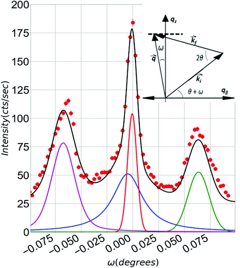 | ||
Fig. 1 Transverse scan at qz = 0.057 Å−1 for sample C4CE using X-rays. The solid curves are from a fit to four components: the two Yoneda23 components are purple and green, the specular is red, the diffuse is blue, and the sum of these (including a linear background term which is not pictured) is shown in black. The inset illustrates the scattering geometry. Here  , ,  are the wavevectors of the incident and reflected beam, respectively, and are the wavevectors of the incident and reflected beam, respectively, and 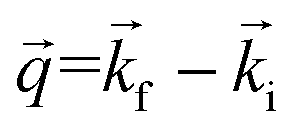 . The dashed line represents a transverse scan across qz and ω is the rocking angle, where ω = 0 is the specular condition at which point qz = 4πsin[2θ/2]/λ. . The dashed line represents a transverse scan across qz and ω is the rocking angle, where ω = 0 is the specular condition at which point qz = 4πsin[2θ/2]/λ. | ||
We also measured extended-range X-ray specular reflectivity (EXRR) which encompasses higher angles that include the Bragg reflections from both the stacking of the graphene layers and the SiC substrate. The diffuse background was obtained by using linear scans at a constant angular offset angle from the specular condition and it was subtracted from the on-specular data. A slight miscut angle between 0.01–0.03° was typically observed (and accommodated in the scans) when comparing the specular condition at grazing angles versus the Bragg reflections. EXRR data are plotted in reciprocal lattice units (rlu) of SiC, l, where l = qzcSiC/2π and cSiC = 10.0848 Å for 4H SiC. Bragg peaks for bulk SiC are expected at l = 4n (n = 1, 2, 3…) and approximately around l = 3m (m = 1, 2, 3…) for graphene.
2.3 Neutron reflectivity
Neutron reflectivity (NR) data was obtained on the reflectometer, BL-4A, at the Spallation Neutron Source (SNS) at Oak Ridge National Laboratory. The SNS is a time of flight source allowing for a range of qz to be measured at a fixed sample angle. Data was collected on a two-dimensional position sensitive detector at room temperature. The data were reduced by integrating a region of interest on the detector along q|| = 0 and subtracting a neighboring parallel region of interest in order to produce the specular line.2.4 Transmission electron microscopy
Transmission electron microscopy (TEM) was obtained from cross-sections of samples that were prepared using a lift-out method in a focused ion-beam scanning electron microscopy (FEI Scios Analytical). A 100 nm thick Pt layer was deposited by a 2 kV electron beam to protect the graphene thin film prior to gallium ion beam exposure. Great care was taken to reduce the Ga ion beam damage and implantation to the graphene thin film by progressively reducing the beam energies and currents in the cleaning cross section mode as the sample gets thinner. The sample cross-sections were then transferred to a 300 kV TEM for imaging. The primary electron beam is incident on the cross-section perpendicular to the surface direction.2.5 Angle resolved photoemission spectroscopy
ARPES was performed using SPECS Phoibos150 analyzer and 21.2 eV photons. The energy and angular resolutions are 20 meV and 0.1° respectively. The base pressure of the ARPES measurement was better than 2 × 10⁻¹⁰ Torr.3 Results
In order to investigate the structure of graphene on 4H-SiC, extended range (EXRR) and grazing angle (XRR) X-ray specular reflectivity was utilized on multiple (8–10) samples. One sample from these was chosen for neutron reflectivity (NR) investigation.3.1 Grazing angle X-ray reflectivity
Specular reflectivity contains structural information related to the scattering length density (SLD) and how it varies (roughness, σ) across the interfaces of layers in the material being studied. In samples where large surface or interface roughness is present, the extraction of the specular component requires care and the issue is twofold: with increasing qz, interface roughness causes the specular reflectivity to decrease while the diffuse scattering increases. The experimental sensitivity to the diffuse scattering also depends on the lateral length-scale of the roughness that causes it. In order to distinguish the specular and diffuse components, transverse scans must be performed at each qz, as illustrated in Fig. 1 where several features can be observed. In addition to the specular component (red) at ω = 0 and a nearby diffuse component (blue) that is slightly off-center from the specular due to the small miscut, Yoneda26 peaks (blue and green) arise from an enhancement of the diffuse scattering when either the incident or outgoing beams is near the angle for total reflection. The broad diffuse scattering component which contributes to the Yoneda scattering is approximated as a linear background over the limited range of the transverse scan and is not pictured in Fig. 1. These components are determined by least-squares fitting of the data to a model where the specular peak is taken as a Gaussian lineshape with a resolution-limited fixed width while the other peaks are taken to be Lorentzian lineshapes. The specular component in these fits is (and must be) resolution limited in width and therefore defined by the instrumental resolution. The specular reflectivity, shown for three samples in Fig. 2(a–c), is generated by using this method to extract the specular component.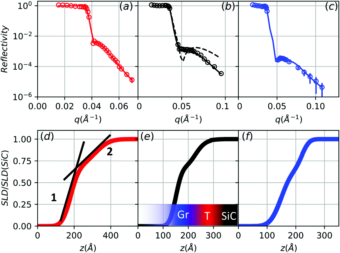 | ||
| Fig. 2 The specular reflectivity measured (open circles) for three samples: (a) 33MO7, (b) C6MO3 and (c) 33MO6 are shown along with the corresponding fits (solid curves) to the model described in the text. The dashed curve in (b) corresponds to a fit using a two-layer model. (d), (e) and (f) show the scattering-length-density (SLD) profiles corresponding to the fitted curves in (a), (b) and (c). The SLD is normalized to 1 at the substrate for clarity. The shading in (e) indicates the layer distribution of the three-layer model where blue is graphene (Gr), red is the transition layer (T), and black is SiC. The lines in (d) demonstrate the difference in the slope of the profile that represents the interfaces, where it can be seen that the buried interface “2” is much broader than the graphene surface roughness “1”. | ||
The XRR data, shown in Fig. 2(a–c), generally exhibit a sharp drop in reflectivity near the critical angle of SiC followed by a weak oscillation due to the graphene film. In order to model the specular reflectivity data it was found that three layers were required, one each for the graphene and the semi-infinite substrate as well as a third “transition layer” in between, as shown schematically in Fig. 3. A simpler model involving only two layers (graphene and SiC) failed to accurately describe the data for most samples, yielding an oscillation that was too strong and with too much intensity after the critical angle, as demonstrated by the dashed curve in Fig. 2(b). This problem was remedied by adding the transition layer, which effectively enabled the introduction of a broader interface between the graphene and the SiC. In a minority of samples a transition layer was unnecessary and a two-layer model was suitable. Adding a fourth layer did not improve the quality of fit. The results of the grazing-angle specular XRR analysis of all samples is given in Table 1.
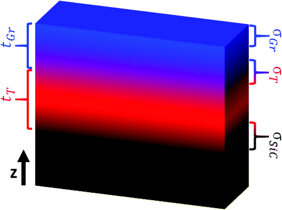 | ||
| Fig. 3 A schematic representation of the three-layer model used to fit the grazing angle specular reflectivity. The blue layer is graphene (Gr), red is a transition layer (T), and black is SiC. tGr and tT are the thicknesses (SiC is semi-infinite) and σGr, σT and σSiC are the interface roughnesses of the respective layers. | ||
| Sample | t Gr (Å) | σ Gr (Å) | t T (Å) | σ T (Å) | SLDT (10−6 Å−2) | σ SiC (Å) |
|---|---|---|---|---|---|---|
| C6M02 | 66(7) | 58(6) | — | — | — | 80(10) |
| C6M04 | 66(7) | 60(8) | 70(10) | 60(10) | 26.6(2) | 1.0(9) |
| 33M07 | 73(9) | 72(8) | — | — | — | 150(20) |
| C4CE | 76(9) | 65(8) | 140(20) | 140(20) | 26.8(2) | 10(9) |
| C6M03 | 77(8) | 46(8) | 70(10) | 70(10) | 27.0(2) | 60(10) |
| C4DF | 82(8) | 82(8) | 150(20) | 140(20) | 26.9(3) | 1.0(9) |
| 33M06 | 94(8) | 78(8) | 120(20) | 40(10) | 27.1(2) | 1.0(9) |
| P8 | 120(20) | 94(10) | 190(20) | 70(10) | 25.1(6) | 100(20) |
| C2 | 340(20) | 185(15) | 330(30) | 70(20) | 21.2(8) | 390(40) |
Fig. 2(d–f) shows the resulting SLD profiles as a function of depth, which reveal the large broadening of the graphene/SiC interface. The general shape of the profile is similar for all samples studied, with no sharp transitions defining the film because of the large roughness at the buried interface. Typically we can identify two distinct slopes, a larger slope associated with the graphene surface and a smaller slope due to the buried interface (“1” and “2”, respectively, in Fig. 2(d)), indicating that the roughness of the buried interface is much larger than at the graphene surface.
This trend becomes more dramatic as a function of graphene thickness, as demonstrated in Fig. 4, where we have quantified the large broadening of the buried interface by defining a “total substrate roughness”, σsub = σT + tT + σSiC. It can be seen that as the sample thickness increases, the roughness at the buried interface (σsub) grows at 2.5 times the rate of the surface roughness of the graphene film (σGr). This result is consistent with the stoichiometry of the sublimation process that consumes 3.14 SiC layers (7.9 Å) for every graphene layer produced (3.37 Å), which amounts to ∼2.4 times the thickness of SiC for every graphene layer.
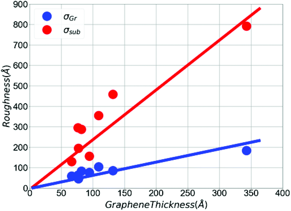 | ||
| Fig. 4 Comparison of the graphene surface roughness and the buried interface roughness at the substrate (as defined in the text) as a function of graphene thickness, obtained from grazing-angle specular reflectivity (XRR) The solid lines are linear fits that are constrained to go through the origin. | ||
3.2 Comparison of grazing-angle neutron and X-ray reflectivity: integrated reflectivity
In order to further investigate the composition of the transition layer that was observed by specular X-ray reflectivity, neutron reflectivity was performed because of its sensitivity to the nuclear SLD that provides different contrast to X-rays. In particular, the neutron scattering length for C is larger than for Si whereas the relative size of these scattering lengths is reversed for X-rays. Fig. 5(a) shows the NR for a sample having 20 atomic layers of graphene and it can be seen that the reflectivity decays very slowly with q. For comparison, the X-ray specular reflectivity measured on the same sample is shown by the open blue circles in Fig. 5(b) where it exhibits a strong precipitous decay with q. The dramatic differences in the q-dependence of the specular XRR and the NR cannot be explained by the composition of the SLDs; rather, the difference can be attributed to the unavoidably lower q|| resolution in the neutron reflectivity measurement as compared with the X-ray measurement. Interestingly, as we will show, this effect has implications well beyond instrumental: the significantly different shape of the reflectivity curves reveal important new information about the lateral length scale of the roughness at the buried interface.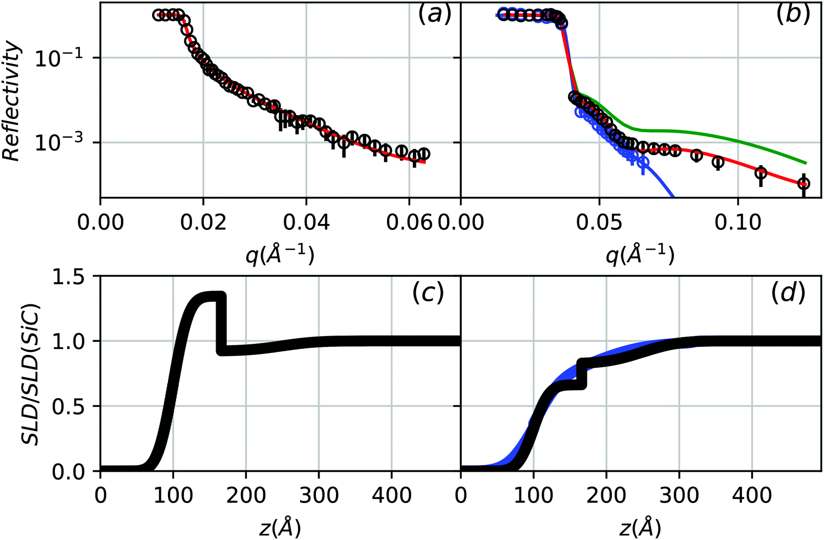 | ||
| Fig. 5 Grazing-angle neutron and X-ray reflectivity measured on the same 20-layer graphene sample (C4CE). (a) Neutron reflectivity (black circles) and (b) X-ray reflectivity for the specular component (blue circles) and the integrated reflectivity (black circles). The solid curves are a fit to the model discussed in the text. The green curve in (b) required the sharp interface to appear at the top of the graphene film rather than between SiC and graphene, as discussed in the text. (c) and (d) are the scattering-length-density profiles determined from the corresponding fitted curves of the same color in (a) and (b), respectively. | ||
Because of the lower q|| resolution in the NR measurement, we compared the NR and XRR by transversely integrating the X-ray reflectivity along q|| over both the specular and diffuse peak (see Fig. 1). The result is shown by the open black circles in Fig. 5(b) and it is apparent that the q-dependence of the integrated X-ray reflectivity behaves quite differently than the specular reflectivity, where the integrated reflectivity persists to much higher q. In fact, both the integrated X-ray reflectivity and the neutron reflectivity, which is instrumentally integrated, behave similarly and their persistence to higher q indicate the presence of a much sharper interface than was determined from the specular X-ray reflectivity. Furthermore, the integration along q|| samples shorter lateral length scales. Therefore, this sharper interface occurs on a much shorter lateral length-scale than the large roughness that was determined by the specular reflectivity of Fig. 2, which samples a much longer lateral length-scale.
The integrated X-ray and neutron reflectivity in Fig. 5 were co-refined using a model that required the physical structure and compositional densities (g cm−3) of the layers of the sample to be identical for both measurements. Because of the spatially abrupt feature now expected in the structure, we found that an additional transition layer was required in the model (four layers) in order to produce a sharp interface. Five layers did not improve the quality of the fit. The fit and resulting SLD profiles are shown in Fig. 5. From the profiles it is clear that the integration of the diffuse scattering now resolves a narrow interfacial structure (roughness <2.5 nm). This narrow feature was determined to be between the graphene layer and transition layer: the green line in Fig. 5(b) shows that requiring the sharp interface to be on top of the film did not accurately describe the data. Several samples were studied using X-ray integrated reflectivity, although only one (C4CE) was studied with both X-rays and neutrons. The results are given in Table 2.
| Sample | SLDGr (10−6 Å−2) | t Gr (Å) | σ Gr (Å) | SLDT (10−6 Å−2) | t T (Å) | σ T (Å) | σ SiC (Å) |
|---|---|---|---|---|---|---|---|
| C4CE(XRR) | 18.0(5) | 66(5) | 40(6) | 22.5(5) | 83(8) | <25 | 92(8) |
| C4CE(Neutron) | 7.0(2) | 66(5) | 40(8) | 4.8(1) | 83(8) | <25 | 92(8) |
| C6M02(XRR) | 18.2(4) | 70(6) | 37(5) | 25.6(4) | 50(6) | <25 | 50(9) |
| C6M03(XRR) | 17.8(5) | 68(4) | 23(5) | 22.8(4) | 65(5) | <25 | 65(8) |
| C6M04(XRR) | 18.0(4) | 63(4) | 24(4) | 22.7(4) | 102(9) | <25 | 110(9) |
| C4DE(XRR) | 18.0(4) | 121(9) | 105(6) | 24.0(5) | 350(20) | <25 | 117(9) |
3.3 Extended-range X-ray reflectivity
X-ray reflectivity was also measured over an extended range (EXRR) of qz, where the larger values of qz have two important consequences: the measurements probe interatomic distances in the direction perpendicular to the surface and there is intrinsically a larger lateral integration of q|| which, according to our grazing angle reflectivity results, should observe flatter interfaces at these shorter lateral length-scales. EXRR data was collected for two orders of SiC reflections and two to three orders of graphene reflections, depending on the sample. A representative subset of the results are shown for three samples in Fig. 6 where qz is given in 4H-SiC reciprocal lattice units (rlu), l.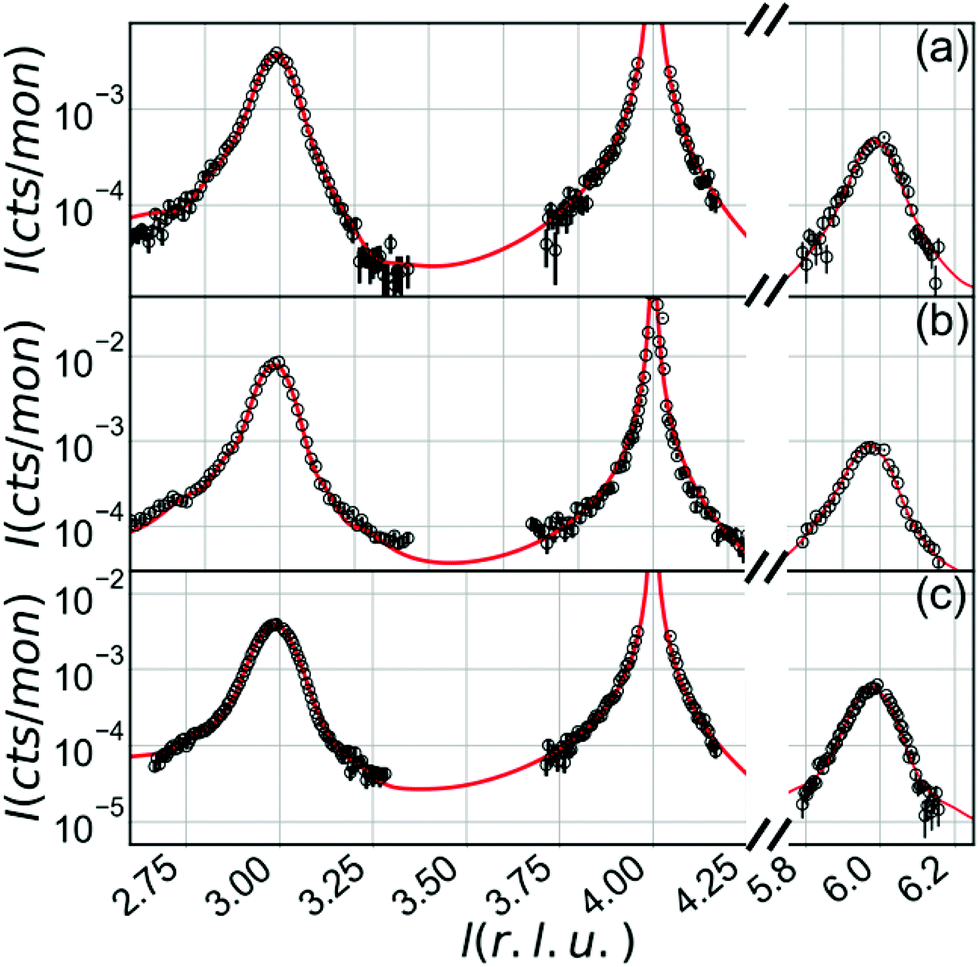 | ||
| Fig. 6 Extended-range X-ray reflectivity data (open circles) along with a fitted model (curve), which is discussed in the text, are shown for three samples: (a) 33MO7, (b) C6MO3 and (c) 33MO6. | ||
The EXRR data was analyzed using a structural model that is illustrated schematically in Fig. 7. In order to fit the data, it was necessary to allow for two vertically stacked graphene layers on top of the carbon-terminated C-face 4H-SiC. A thin graphene bottom layer, “B”, having NB atomic sheets with a slightly expanded inter-planar spacing dBGr is located near the SiC substrate while the majority of the graphene resides in the “T” layer having NT atomic sheets with inter-planar spacing dTGr.
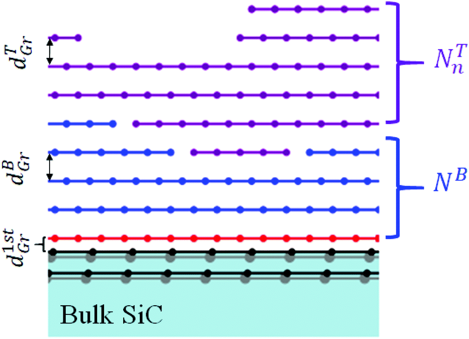 | ||
| Fig. 7 Schematic representation of the model that is used to describe the EXRR data. The epitaxial graphene is considered in terms of two layers that have slightly different spacing between the graphene atomic sheets: a very thin bottom layer “B” consisting of NB graphene atomic sheets with spacing dBGr and a thicker top layer “T” having three different height distributions, NTn (with n = 1, 2, 3), and a spacing dTGr. The two atomic bilayers in bulk SiC show the carbon (black circles) truncation of the substrate. | ||
The reflectivity in the kinematic approximation is obtained by adding the contributions of each layer:
 | (1) |
It was necessary to include a small amount of disorder through a root-mean-square (RMS) fluctuation of the inter-planar distance between the atomic sheets of graphene, ΔdBGr and ΔdTGr, for the bottom and top graphene layers, respectively. The number of atomic graphene sheets, NB and NT for the bottom and top graphene layers, respectively, also exhibit fluctuations and these were modeled† as a binomial distribution with corresponding roughness values of σB and σT. In the case of the top layer, additional height distributions were required to describe σT, as discussed in the ESI.† The results of the analysis for all samples is summarized in Table 3. The thermal Debye–Waller factor at room-temperature for graphite is expected to be 0.05–0.095 Å (ref. 27) which is comparable to ΔdTGr for our samples; but ΔdBGr was found to be larger, indicating more disorder near the graphene/SiC interface.†
| Sample |
![[N with combining macron]](https://www.rsc.org/images/entities/i_char_004e_0304.gif) (layers) (layers) |
L, domain size (Å) | d TGr (Å) | ΔdTGr (Å) | d BGr (Å) | ΔdBGr (Å) | N B (layers) |
|---|---|---|---|---|---|---|---|
| 33M06 | 17(2) | 6600(200) | 3.368(6) | 0 | 3.41(3) | 0.13(2) | 4.1(3) |
| 33M07 | 16(2) | 6400(200) | 3.367(6) | 0 | 3.39(2) | 0.16(2) | 4.1(3) |
| C2 | 53(3) | 2900(200) | 3.372(6) | 0.07(2) | 3.38(1) | 0.06(2) | 14.3(5) |
| C4CE | 14(2) | 6800(200) | 3.368(6) | 0.10(2) | 3.42(3) | 0.16(2) | 4.6(4) |
| C4DE | 33(2) | 8300(300) | 3.373(7) | 0.06(2) | 3.39(3) | 0.10(2) | 4.9(4) |
| C4DF | 16(2) | 5700(200) | 3.370(6) | 0.03(2) | 3.42(3) | 0.21(4) | 2.8(4) |
| C4M05 | 24(2) | 5700(200) | 3.373(6) | 0.13(3) | 3.41(3) | 0.24(3) | 2.8(4) |
| C6M02 | 18(2) | 8000(300) | 3.367(6) | 0.06(2) | 3.41(3) | 0.14(2) | 3.2(4) |
| C6M03 | 22(2) | 10300(300) |
3.373(6) | 0.09(3) | 3.39(2) | 0.14(2) | 7.1(5) |
| C6M04 | 20(2) | 10300(300) |
3.373(6) | 0.10(4) | 3.41(3) | 0.24(4) | 2.5(5) |
| P8 | 29(4) | 7400(300) | 3.367(6) | 0.07(3) | 3.40(3) | 0.21(3) | 5.2(4) |
The graphene lateral domain size, L, of the film can be determined from transverse scans (rocking scans, as shown in the inset of Fig. 1) performed at the graphene Bragg positions. Unlike at grazing angles, the specular width is not resolution-limited and the broadening is due to the finite crystalline domain size (laterally) of the graphene. It can be shown that transverse angular width Δω will vary as a function of qz according to Δω = [(2π/qzL)2 + η2]1/2 where a mosaic-like rotational disorder η is included.28 The results are illustrated in Fig. 8 for three samples and this method was used to determine the graphene domain sizes for all samples shown in Table 3. As can be seen from Table 3, the graphene domain sizes vary between 0.5–1.0 μm.
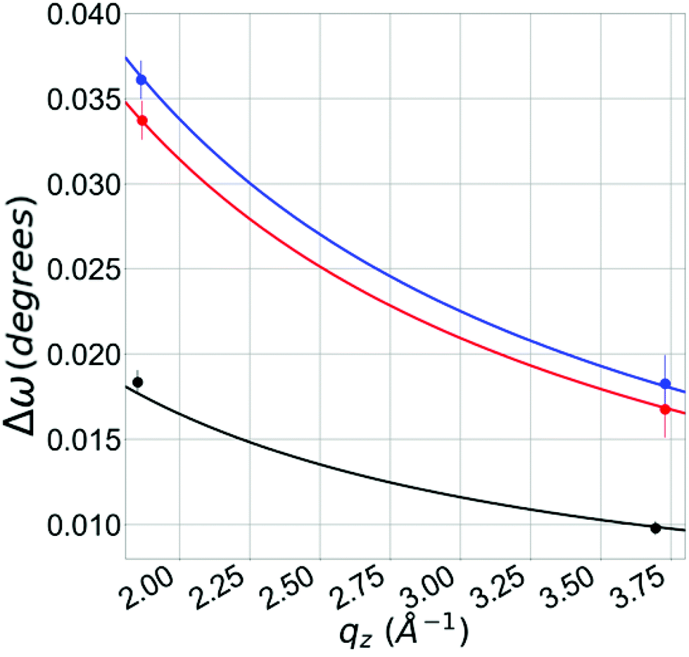 | ||
| Fig. 8 The transverse angular width of graphene Bragg peaks versus wavevector, shown for three samples: C6MO3 (black), C4CE (red), and C4DF (blue). The solid curves relate these widths to the graphene domain size, as discussed in the text. | ||
3.4 Cross-sectional transmission electron microscopy
Electron microscopy provided additional insight into the local buried interface structure. Representative high-resolution TEM (HR-TEM) images for a sample (C4, not studied by X-rays) having 60 layers of graphene are shown in Fig. 9. In Fig. 9(a) it can be seen that the graphene layers exhibit a wavy structure, particularly in comparison to the atomically uniform planes of the SiC. The RMS variation of these graphene planes is much larger than the ΔdTGr determined from any of the EXRR measurements, indicating some disruption of the graphene atomic planes during the sectioning of the sample for the TEM measurements. Beam damage has also been reported in prior TEM measurements by Colby et al. on similar samples.29 The EXRR measurements give a global quantitative indication of the RMS fluctuations without perturbing the sample and it is noted that the lateral crystalline domain size of the graphene found by X-ray diffraction is much larger than the field of view of the TEM image. One can see a thin graphene layer adjacent to the SiC substrate with a thickness that is consistent with the NB values observed in the EXRR measurements. It is also observed in Fig. 9(a) that the SiC/graphene interface is abrupt on the atomic scale. Nevertheless, as observed in Fig. 9(b), large steps on the order of 10 nm in height can be observed at the interface, disrupting an otherwise atomically flat interface between graphene and the SiC substrate. Here it can be seen that the graphene film follows the contour of these large step edges of the substrate. In addition, local defects as in Fig. 9(c), which have been previously identified as vents for the escape of Si during the sublimation process, can also be found.30 These results support the interpretation of the specular XRR and the EXRR measurements: the former averages lateral length-scales on the order of 50 μm and finds very broad interfaces that are several tens of nm in height whereas the latter averages <5 μm laterally and observes much sharper interfaces. However, the limited field of view of microscopy makes it difficult to understand the frequency of occurrence of these features and their overall contribution to the interface roughness.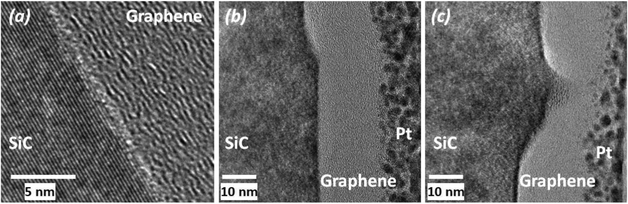 | ||
| Fig. 9 HR-TEM cross sections for a sample having 60 layers of graphene. In (a) the graphene atomic planes are observed while a thin transition layer of a few atomic graphene planes appears near the interface with SiC. The SiC exhibits atomically uniform crystalline planes. In (b) a large step in the substrate is observed while the graphene film is found to follow the step. In (c) a defect in the film illustrates both the need for an extremely broad distribution of buried interface heights as well as an accumulation of Si near the defect site. | ||
4 Discussion
These results show that the buried interface between graphene and C-face SiC exhibits a complex behavior that is manifested on two lateral length scales along the interface. At shorter length scales there is an atomically abrupt transition between the SiC and the graphene layer whereas the interface displays extensive roughness over much longer lateral length scales. Below, we discuss the interpretation of these results. In particular, an important aspect of this investigation is that it also demonstrates how such information can be obtained by X-ray and neutron reflectivity measurements. Most studies that utilize reflectivity do not carefully consider the implications of diffuse scattering. Here, however, we find that the diffuse scattering informs both the interpretation of interfacial structure as well as how to analyze the reflectivity data so that this investigation can be useful for a broad range of materials systems that have complex interfaces.The X-ray specular reflectivity (XRR) measurements performed at grazing angles reveal a very rough buried interface between graphene and the SiC, as observed in Fig. 2. The width of this interface grows proportionally to the thickness of the graphene that is produced (see Fig. 4), indicating that the origin of the roughness is from the growth process itself. Indeed, it takes22 more than three atomic layers of SiC to produce one atomic layer of graphene so that the interface roughness is driven by the sublimation of Si. This effect is significant and the buried interface width can be larger than the total thickness of the graphene that is produced. By comparison, the surface roughness of the graphene (Fig. 4) is nearly three times smaller, suggesting that the roughness at the buried interface is driven by the lateral variations in the local growth rate. The lateral length-scale over which this interface roughness is observed can be estimated from the relatively high reciprocal-space resolution of these measurements: at q = 0.1 Å−1 the measurements of the specular reflection average about 50 μm laterally. Over this distance many asperities can be encountered at the buried interface, such as large steps and Si vents, as seen by HR-TEM in Fig. 9(b) and (c), so that these sublimation-induced features are expected to be responsible for the large roughness observed at the buried interface.
In stark contrast, X-ray reflectivity measured over an extended angular range that includes Bragg reflections (EXRR) reveals an atomically abrupt interface between the graphene and the SiC (see Fig. 6 and 7). The reason for this result relates to both the specific nature of the disorder at the buried interface and to the lower reciprocal-space resolution in EXRR measurements as compared to specular XRR.
To better understand this point and the structure of the buried interface, it is useful to look more closely at the XRR measurements. Central to this issue is a diffuse scattering peak that appears near the specular reflection in Fig. 1, which generally arises from laterally-correlated interfacial disorder.26 A plot of the width of this diffuse scattering peak, Δq||, versus qz for a sample with 55 layers of graphene is shown in Fig. 10. It reveals a curve having a shape that is well-known to arise from a random distribution of flat terraces. A fit to a model31 yields the average length of a flat terrace to be 650 nm. Therefore, we would expect large flat regions to exist despite the XRR results in Fig. 2 and 4 that indicate a very broad buried interface. This apparent contradiction is resolved by integrating both the specular and diffuse component when compiling the XRR data, which was done in Fig. 5(b). As can be seen, the integrated XRR leads to a sharp buried interface in the scattering-length-density profile in Fig. 5(d) as compared to the profile of the broad buried interface that was obtained using only the specular component. By including the integrated diffuse component, the reflectivity then measures the SLD over a lateral length-scale that is shorter than the length of a flat terrace, thereby giving a sharp interface.
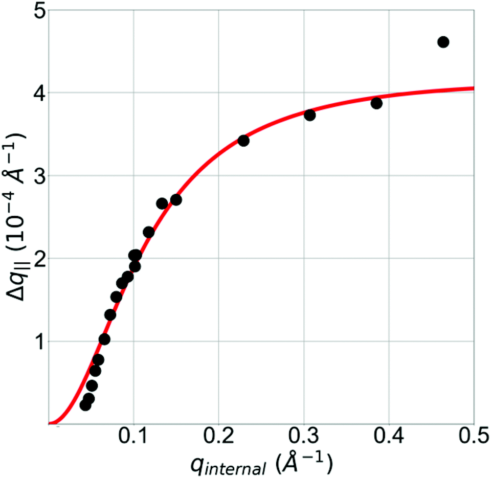 | ||
| Fig. 10 The width of the diffuse scattering peak versus perpendicular wavevector transfer is shown (symbols) for a sample having 55 layers of graphene. qinternal is qz corrected for refraction. These data reveal the presence of a random distribution of large flat terraces at the buried interface. The solid curve is a fit to a model given in eqn (21) of ref. 31 using γ = 0.00016, α = 0.43 and t = 5.04, which yields an average terrace length of 650 nm. | ||
This new understanding of the diffuse scattering allows us to interpret the neutron reflectivity results in Fig. 5(a) and (c). Because the lateral resolution in the neutron reflectivity measurement was much poorer than for the X-ray measurement, the diffuse scattering from the terraces, which appears very near the specular reflection, is unavoidably integrated in the neutron measurement. Therefore, the SLD profile (Fig. 5(c)) obtained from the neutron measurement exhibits a sharp buried interface just as in the integrated XRR measurement.
Having confidence in the similarity of the integrated XRR and the NR data allowed us to perform a co-refinement of both data sets, which yielded the SLD profiles shown in Fig. 5(c) and (d). We are also able to directly obtain the composition of C and Si from this analysis. It is noted that from a single SLD profile we do not know the relative contributions of C and Si to the SLD because we do not know the densities of each element, ρC or ρSi, respectively. However, having both the X-ray and the neutron data with the co-refinement allows us to solve for these densities using the known scattering lengths for these elements, bXC and bXSi for X-rays and bNC and bNSi for neutrons. The SLD is comprised of both elements according to:
| SLDNeutron = bNCρC + bNSiρSi, | (2) |
| SLDX-ray = bXCρC + bXSiρSi. | (3) |
The result of using both SLD measurements to obtain the densities of the atomic species is shown in Fig. 11, where it can be seen that there is a remarkably sharp interface between the graphene and the SiC substrate (which is essentially represented by the Si density). The slight variation of the Si density in the substrate is an artifact of not integrating additional diffuse scattering from the short length-scale asperities at the interface that we know are present from the very large roughness in the specular XRR and which also appear in the TEM (e.g.Fig. 9(b) and (c)). This diffuse scattering will be very broad in angle; for example it is that diffuse scattering which gives rise to the Yoneda scattering in Fig. 1 and it is, therefore, impractical to capture all of the intensity. In our analysis, that diffuse scattering contribution has been subtracted out from our integrated XRR.
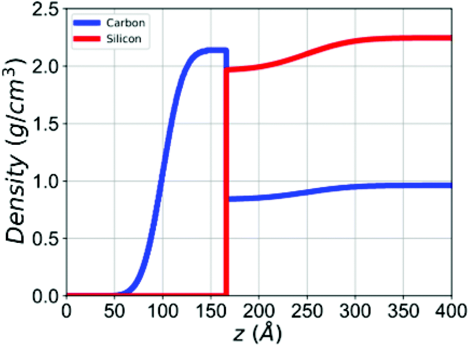 | ||
| Fig. 11 An abrupt interface is observed in the density profile, which was determined separately for C and Si from the co-refinement of the X-ray and neutron reflectivity in Fig. 5. | ||
Understanding the origin of the diffuse scattering also allows us to explain why EXRR measurements reveal an atomically abrupt buried interface rather than the highly rough interface found from grazing-angle reflectivity. Because the EXRR measurements are performed at higher qz, they intrinsically have a lower lateral resolution in reciprocal space where the diffuse component is more easily integrated during the measurement; therefore, EXRR measurements represent the atomic scale structure relative to the long and flat terraces rather than the structures that lead to a large roughness. For example, previous synchrotron EXRR measurements on substantially thinner graphene films report atomically abrupt interfaces with a slight carbon enrichment of the first three SiC layers at the interface.21 These sharp interfaces are measured despite the fact that the X-rays irradiate a macroscopic sample having large interface roughness. Other measurements, such as HR-TEM can select regions that show near perfect interfaces; however, electron microscopy does not have the field of view to put the various features found in Fig. 9 into context. We have shown here that understanding the step structure allows us to use different measurements (XRR, NR, EXRR) to tie the vastly different aspects of this complex buried interface together.
Interestingly, the step structure appears not to change with extensive sublimation. A synchrotron X-ray scattering study on much thinner epitaxial graphene films on C-face SiC (7 times thinner) has observed diffuse scattering nearly identical in shape and magnitude to that shown in Fig. 10.32 This similarity indicates that the step structure is intrinsic to the SiC and it does not significantly change upon sublimation; rather, it is the size and/or number of surface asperities that increases with longer sublimation times in order to produce the highly rough interface while the atomically flat regions are left intact, although, there will be fewer of them as the graphene film thickness increases.
Our study also reveals important aspects of the thick epitaxial multilayer graphene that were not apparent in previous studies of thinner graphene layers. As can be seen from Table 3, the first 1–2 nm of graphene layers near the interface with SiC have a slightly expanded interlayer spacing compared to the majority of the layers away from that interface, dBGr > dTGr. Interestingly the value of dBGr, which exhibits variations among samples, extends to a range which is comparable to turbostatic graphite (d = 3.440 Å) and thus suggests stacking disorder close the interface where the most recently formed graphene exists. It seems that this disorder anneals away during the growth of more graphene from below as the majority of the graphene exhibits consistent values of dTGr among samples of different thicknesses. This results is also consistent with previous studies done on thinner graphene films on C-face 4H SiC where the graphene interlayer spacing was found to be slightly larger than for graphite (3.354 Å) because of epitaxial multilayer graphene's stacking rotations (which are different than graphite).21 Our model for the EXRR data allows for RMS variations of the interlayer spacing where we find that ΔdBGr is typically significantly larger than ΔdTGr, which was found to take on the thermal value. Therefore, this result also suggests more disorder in the several layers of graphene near the substrate. That the high structural quality of the top graphene layers is preserved can be seen in an ARPES measurement shown in Fig. 12, where the Dirac cone can be observed, indicating the non-graphitic stacking of graphene on C-face SiC.19
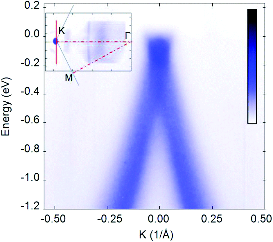 | ||
| Fig. 12 ARPES spectrum taken from 20 layers of epitaxial graphene on C-face SiC. This spectrum is on a line cut through the K point in the graphene Brillouin zone, indicated by the red solid line in the upper left corner. Fermi surface mapping from Γ point to the K point is shown in the upper left corner, where the small blue circle is the upper Dirac cone cut by the Fermi energy. The red dashed lines indicate the Γ–K and Γ–M high symmetry line in the Brillouin zone. A second derivative taken from this spectrum shows multiple closely space Dirac cones, indicating the non-graphtitic stacking of the graphene layers near the surface. | ||
5 Summary
In summary, we have found that there are two length-scale regimes that characterize the buried interface of epitaxial multilayer graphene grown on C-face 4H-SiC. On long length scales, a very large roughness develops at the buried interface growth front in proportion to the graphene thickness, which is due to the sublimation of Si. However, the interface is atomically abrupt on shorter length scales due to the intrinsic flatness of SiC terraces which are preserved during the growth of multilayer graphene. We showed that the existence of these two length scales is manifested in the nature of the diffuse scattering that is present in reflectivity measurements and by carefully considering these effects we showed that we could employ complimentary X-ray and neutron reflectivity to obtain the composition profile of C and Si at the buried interface. In general, diffuse scattering is usually not carefully considered in reflectivity measurements and our results show that the conclusions drawn from such data can depend critically on how the diffuse scattering is handled. The lessons learned in this study will be valuable for informing other studies of complex interfaces that are present in many material systems of interest.Conflicts of interest
There are no conflicts to declare.Acknowledgements
This research was supported by the National Science Foundation under Grant No. DGE-1069091, Oak Ridge National Lab's Graduate Opportunities! Program, and by the Department of Energy (DOE) Office of Science Graduate Student Research. A portion of this research used resources at the Spallation Neutron Source, a DOE Office of Science User Facility operated by the Oak Ridge National Laboratory. The TEM work was supported by the University of Missouri Electron Microscopy Core Excellence in Electron Microscopy award.References
- C. Berger, Z. Song, X. Li, X. Wu, N. Brown, C. Naud, D. Mayou, T. Li, J. Hass, A. N. Marchenkov, E. H. Conrad, P. N. First and W. A. de Heer, Science, 2006, 312, 1191–1196 CrossRef CAS PubMed.
- K. Bolotin, K. Sikes, Z. Jiang, M. Klima, G. Fudenberg, J. Hone, P. Kim and H. Stormer, Solid State Commun., 2008, 146, 351–355 CrossRef CAS.
- H. Chen, M. B. Mãijller, K. J. Gilmore, G. G. Wallace and D. Li, Adv. Mater., 2008, 20, 3557–3561 CrossRef CAS.
- S. Stankovich, D. A. Dikin, G. H. B. Dommett, K. M. Kohlhaas, E. J. Zimney, E. A. Stach, R. D. Piner, S. T. Nguyen and R. S. Ruoff, Nature, 2006, 442, 282–286 CrossRef CAS PubMed.
- Y. Shao, J. Wang, H. Wu, J. Liu, I. Aksay and Y. Lin, Electroanalysis, 2010, 22, 1027–1036 CrossRef CAS.
- W. Han, R. K. Kawakami, M. Gmitra and J. Fabian, Nat. Nanotechnol., 2014, 9, 794–807 CrossRef CAS PubMed.
- P. Salvo, B. Melai, N. Calisi, C. Paoletti, F. Bellagambi, A. Kirchhain, M. Trivella, R. Fuoco and F. Di Francesco, Sens. Actuators, B, 2018, 256, 976–991 CrossRef CAS.
- V. Singh, D. Joung, L. Zhai, S. Das, S. I. Khondaker and S. Seal, Prog. Mater. Sci., 2011, 56, 1178–1271 CrossRef CAS.
- A. N. Grigorenko, M. Polini and K. S. Novoselov, Nat. Photonics, 2012, 6, 749–758 CrossRef CAS.
- A. Charrier, A. Coati, T. Argunova, F. Thibaudau, Y. Garreau, R. Pinchaux, I. Forbeaux, J.-M. Debever, M. Sauvage-Simkin and J.-M. Themlin, J. Appl. Phys., 2002, 92, 2479–2484 CrossRef CAS.
- W. A. de Heer, C. Berger, M. Ruan, M. Sprinkle, X. Li, Y. Hu, B. Zhang, J. Hankinson and E. Conrad, Proc. Natl. Acad. Sci. U. S. A., 2011, 108, 16900–16905 CrossRef CAS PubMed.
- J. D. Emery, B. Detlefs, H. J. Karmel, L. O. Nyakiti, D. K. Gaskill, M. C. Hersam, J. Zegenhagen and M. J. Bedzyk, Phys. Rev. Lett., 2013, 111, 1–5 CrossRef PubMed.
- J. D. Emery, V. D. Wheeler, J. E. Johns, M. E. McBriarty, B. Detlefs, M. C. Hersam, D. Kurt Gaskill and M. J. Bedzyk, Appl. Phys. Lett., 2014, 105, 161602 CrossRef.
- J. Hass, J. E. Millãąn-Otoya, P. N. First and E. H. Conrad, Phys. Rev. B: Condens. Matter Mater. Phys., 2008, 78, 1–10 CrossRef.
- J. Park, W. Mitchel, H. Smith, L. Grazulis and K. Eyink, Carbon, 2010, 48, 1670–1673 CrossRef CAS.
- N. P. Guisinger, G. M. Rutter, J. N. Crain, P. N. First and J. A. Stroscio, Nano Lett., 2009, 9, 1462–1466 CrossRef CAS PubMed.
- M. Conrad, F. Wang, M. Nevius, K. Jinkins, A. Celis, M. Narayanan Nair, A. Taleb-Ibrahimi, A. Tejeda, Y. Garreau, A. Vlad, A. Coati, P. F. Miceli and E. H. Conrad, Nano Lett., 2017, 17, 341–347 CrossRef CAS PubMed.
- M. Nevius, M. Conrad, F. Wang, A. Celis, M. Nair, A. Taleb-Ibrahimi, A. Tejeda and E. Conrad, Phys. Rev. Lett., 2015, 115, 1–5 CrossRef PubMed.
- J. Hass, F. Varchon, J. E. Millãąn-Otoya, M. Sprinkle, N. Sharma, W. A. de Heer, C. Berger, P. N. First, L. Magaud and E. H. Conrad, Phys. Rev. Lett., 2008, 100, 1–4 CrossRef PubMed.
- A. Tejeda, A. Taleb-Ibrahimi, W. de Heer, C. Berger and E. H. Conrad, New J. Phys., 2012, 14, 125007 CrossRef.
- J. Hass, R. Feng, J. E. Millãąn-Otoya, X. Li, M. Sprinkle, P. N. First, W. A. de Heer, E. H. Conrad and C. Berger, Phys. Rev. B: Condens. Matter Mater. Phys., 2007, 75, 1–8 CrossRef.
- J. Hass, W. A. de Heer and E. H. Conrad, J. Phys.: Condens. Matter, 2008, 20, 323202 CrossRef.
- W. Weber and B. Lengeler, Phys. Rev. B: Condens. Matter Mater. Phys., 1992, 46, 7953–7956 CrossRef PubMed.
- M. Nevius, Improved Growth, ordering, and characterization of sidewall epitaxial graphene nanoridbbons, Ph.D. thesis, Georgia Institute of Technology, 2016 Search PubMed.
- P. Kienzle, K. O'Donovan, J. Ankner, N. Berk and C. Majkrzak, Reflpak, 2000, http://www.ncnr.nist.gov/reflpak Search PubMed.
- S. K. Sinha, E. B. Sirota, S. Garoff and H. B. Stanley, Phys. Rev. B: Condens. Matter Mater. Phys., 1988, 38, 2297–2311 CrossRef PubMed.
- T. Haridasn and G. Sathyamurthy, IEEE Trans. Plasma Sci., 1976, 4, 301–302 Search PubMed.
- W. C. Elliott, P. F. Miceli, T. Tse and P. W. Stephens, Phys. Rev. B: Condens. Matter Mater. Phys., 1996, 54, 17938–17942 CrossRef CAS PubMed.
- R. Colby, M. L. Bolen, M. A. Capano and E. A. Stach, Appl. Phys. Lett., 2011, 99, 101904 CrossRef.
- N. Camara, G. Rius, J.-R. Huntzinger, A. Tiberj, L. Magaud, N. Mestres, P. Godignon and J. Camassel, Appl. Phys. Lett., 2008, 93, 263102 CrossRef.
- T.-M. Lu and M. Lagally, Surf. Sci., 1982, 120, 47–66 CrossRef CAS.
- J. Hass, R. Feng, T. Li, X. Li, Z. Zong, W. A. de Heer, P. N. First, E. H. Conrad, C. A. Jeffrey and C. Berger, Appl. Phys. Lett., 2006, 89, 143106 CrossRef.
Footnote |
| † Electronic supplementary information (ESI) available. See DOI: 10.1039/c9nr03504d |
| This journal is © The Royal Society of Chemistry 2019 |