
 Open Access Article
 This Open Access Article is licensed under a Creative Commons Attribution-Non Commercial 3.0 Unported Licence
Stress transfer at the nanoscale on graphene ribbons of regular geometry†
A. C.
Manikas
 ab,
M. G.
Pastore Carbone
a,
C. R.
Woods
c,
Y.
Wang
c,
I.
Souli
a,
G.
Anagnostopoulos
a,
M.
Hadjinicolaou
d,
K. S.
Novoselov
c and
C.
Galiotis
*a
ab,
M. G.
Pastore Carbone
a,
C. R.
Woods
c,
Y.
Wang
c,
I.
Souli
a,
G.
Anagnostopoulos
a,
M.
Hadjinicolaou
d,
K. S.
Novoselov
c and
C.
Galiotis
*a
aInstitute of Chemical Engineering, Foundation for Research and Technology Hellas (ICEHT/FORTH), Stadium St., Platani, 26504, Patras, Greece. E-mail: c.galiotis@iceht.forth.gr
bDepartment of Chemical Engineering, University of Patras, Patras 26504, Greece
cSchool of Physics and Astronomy, University of Manchester, Manchester, UK
dHellenic Open University, School of Science and Technology, Applied Mathematics Laboratory, Patras, Greece
First published on 15th July 2019
Abstract
The knowledge of the mechanism of stress transfer from a polymer matrix to a 2-dimensional nano-inclusion such as a graphene flake is of paramount importance for the design and the production of effective nanocomposites. For efficient reinforcement the shape of the inclusion must be accurately controlled since the axial stress transfer from matrix to the inclusion is affected by the axial-shear coupling observed upon loading of a flake of irregular geometry. Herein, we study true axial phenomena on regular- exfoliated-graphene micro-ribbons which are perfectly aligned to the loading direction. We exploit the strain sensitivity of vibrational wave numbers in order to map point-by-point the strain built up along the length of graphene. By considering the balance of shear-to-axial forces, we identify the shear stress at the interface and develop a universal inverse-length parameter that governs the stress transfer process at the nanoscale. An important parameter that has come out of this approach is the prediction and measurement of the transfer length that is required for efficient stress in these systems.
Introduction
Graphene is a perfect 2-dimensional crystal of covalently bonded carbon atoms that is a promising candidate for a number of electrical, thermal and mechanical applications, due to its exceptional physical properties.1 Its impressive mechanical properties2 have made graphene an obvious candidate for the use in high-performance polymer-based composites. For the fabrication of composite or hybrid materials, several transfer methods have been proposed for the deposition of the flakes on specific locations of the substrate3 which can integrate graphene sheets with a wider variety of materials. However, ripples, wrinkles or folds and even chemical doping can be induced through the transfer process. One problem associated with Exfoliated Graphene (EG) samples is that physical measurements are normally performed on non-uniformly strained flakes of irregular geometry which are loaded in tension; this can lead to a non-uniform strain distribution4 that may promote premature failure (Fig. 1a). Furthermore, Poisson's contraction in the transverse direction upon tensile loading will induce orthogonal buckling5,6 when a certain critical value is reached, thus making pure axial measurements untenable (Fig. 1b).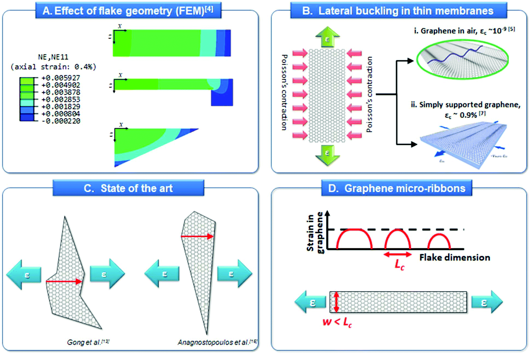 | ||
| Fig. 1 Application of uniaxial stress to graphene flakes of various shapes and geometries. (A). FEM analysis shows that, under uniaxial loading, non-uniform strain distributions result by transverse Poisson's ratio effects due to the irregular geometry of EF flakes.4 (B) For typical rectangular flakes, axial tension will immediately induce lateral buckling due to Poisson's contraction making the attainment of pure axial experiments questionable. (C) Previous investigation of stress transfer in graphene/polymer systems has been performed on flakes with highly irregular shape. (D) The design of graphene micro-ribbons, of widths larger than the critical length (lc), is the key to overcome such issues. Fig. 1A adapted from ref. 4 with permission from ASME. | ||
The performance and reliability of 2-dimensional material-based devices are often limited by the interfacial properties between graphene and substrate materials. An important question that comes out at this point is whether an external stress field applied to the substrate itself can be transferred partially or fully to the simply supported or fully embedded graphene. This is not a trivial question since bending or stretching of the substrate may affect the overall stress carried by the 2-dimensional material which, in turn, could affect its performance and may indeed lead to premature fracture or detachment. In order to assess the stress or strain built up along a graphene flake, it is necessary to employ a technique that is capable to measure strain at the nanoscale. Raman spectroscopy has been successfully adopted to investigate stress transfer in a variety of composites reinforced with carbon-based materials such as graphene,7–10 carbon fibres11,12 and carbon nanotubes13–17 and this is based on the stress/strain sensitivity of their Raman spectra. The Raman spectra of crystalline inclusions have been found to shift under the imposition of stress or strain. This physical phenomenon is due to the anharmonic nature of the chemical bonds and the consequent change of their force constant with bond axial extension (ESI†). Since the Raman frequencies are related to the force constants then an independent calibration curve between Raman shifts and stress or strain can be constructed;18,19 this can then be used to revert to values of stress or strain in the inclusion when the latter is subjected to mechanical load by the substrate or matrix (ESI†)11 The first attempts to assess the strain transfer in EG embedded in a polymer matrix7,8 showed that, upon imposing of the external (tensile) stress field, the stress was built up on the flakes by a shear-lag process. This early work verified the applicability of macroscopic theories to the stress transfer at the nanoscale but, due to the lack of sufficient experimental data points near the flake ends, the exact shape of stress transfer curves could not be fully identified. This may explain the rather large transfer lengths obtained through their analysis (of the order of a few microns) for materials of less than 1 nm in thickness. Furthermore, tensile experiments20 have been performed on simply supported graphene/PET systems and found that the axial stress was transferred to the graphene flakes by a shear lag mechanism. In that case, for low strains, transfer lengths of ca. 2 μm were measured. Recently, some of the authors have conducted a detailed Raman line mapping near the edges of a supported monolayer EG flake, showing that the distribution of axial strain (stress) along the flake deviates somewhat from the classical shear-lag prediction for a region of ∼2 μm from the edge8 due to unintentional doping, and/or edge effects. It is worth noting here that in all cases, the analysis of the stress transfer mechanism was not rigorous due to the irregular shapes of graphene flakes and the lack of alignment in the loading direction (Fig. 1c).
The rectangular geometry of graphene micro-ribbons ensures a uniform stress distribution along the loading direction and prevents lateral buckling due to Poisson's contraction, which is a common occurrence in thin membranes under uniaxial loading (Fig. 1d). Only such a geometry provides reliable results regarding axial stress transfer between graphene and a polymer substrate. It is important to note here that graphene micro-ribbons are currently attracting attention in several applications, such as metamaterials,21,22 waveguiding strain sensoring,23 chemiresistors,24 microsupercapacitors,25 and could be exploited also as efficient reinforcement in composite materials. In this work, we conduct a systematic study of the stress/strain transfer profiles in fully embedded graphene micro-ribbon/PMMA systems under incremental tensile loading.
Results and discussion
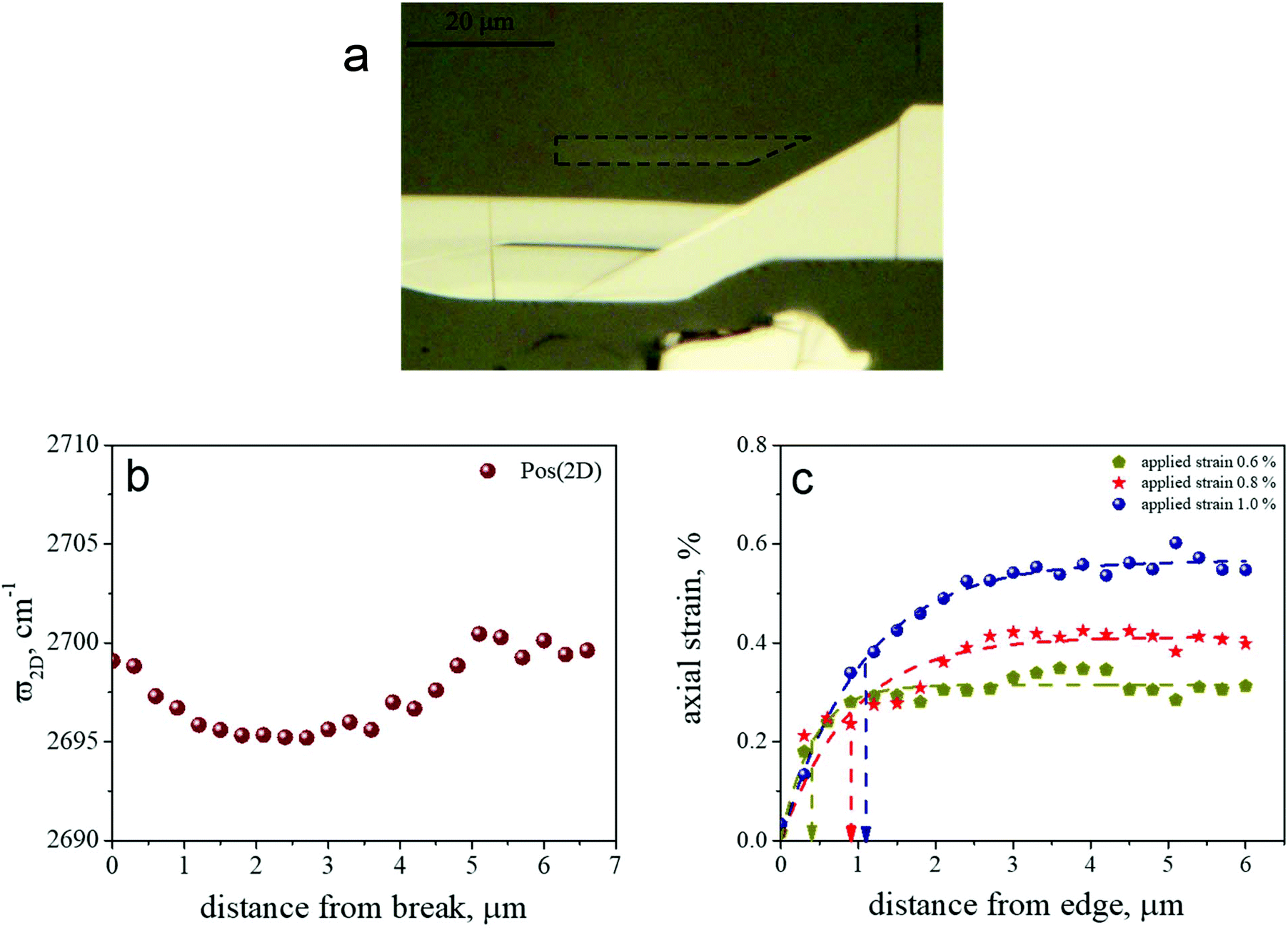
The embedded flake under investigation has been transferred to the PMMA beam by wet transfer.26 As shown in Fig. 2a, the flake is a micro-ribbon having a length of ca. 70 μm and a width of ca. 6 μm. During the transfer process, care was taken to ensure the alignment of the ribbon to the longitudinal axis of the PMMA beam. The exact nature of the flakes was identified by the corresponding Raman spectra of the 2D peak (Fig. S1†). The position of the 2D peak at the unstressed state of the flake was found at 2692 cm−1 with FWHM of 29 cm−1 and the ratio I2D/IG ∼ 5. These results confirm that the examined ribbon is a monolayer graphene subjected to a small residual compressive strain.27 All experiments were conducted at the left-hand end of the ribbon, that is in direct contact with the polymer, and laser Raman sampling was conducted along the longitudinal axis of the ribbon and up to a distance of 9 μm. Since stress transfer in all composite systems is activated at the edges of the embedded reinforcement then care is taken to sample the Raman spectra at steps of 350 nm starting from the edge of the ribbon and moving inwards. The detailed line Raman mapping of the pristine embedded micro-ribbon shown in Fig. 2b reveals that the micro-ribbon experiences residual compressive stress resulting from sample preparation. In fact, the spatial distribution of the frequency positions for both ω2D and ωG modes is non-uniform, thus suggesting that the micro-ribbon is not perfectly flat and seems to be exhibiting an inhomogeneous strain distribution up to −0.12%. The observed variation in strain could be the indication of the presence of ripples and wrinkles which could have been induced by the transfer process and the polymer solidification. Unfortunately, the presence of the transfer layer prevents the direct observation of the corrugations by imaging techniques such as SEM or AFM.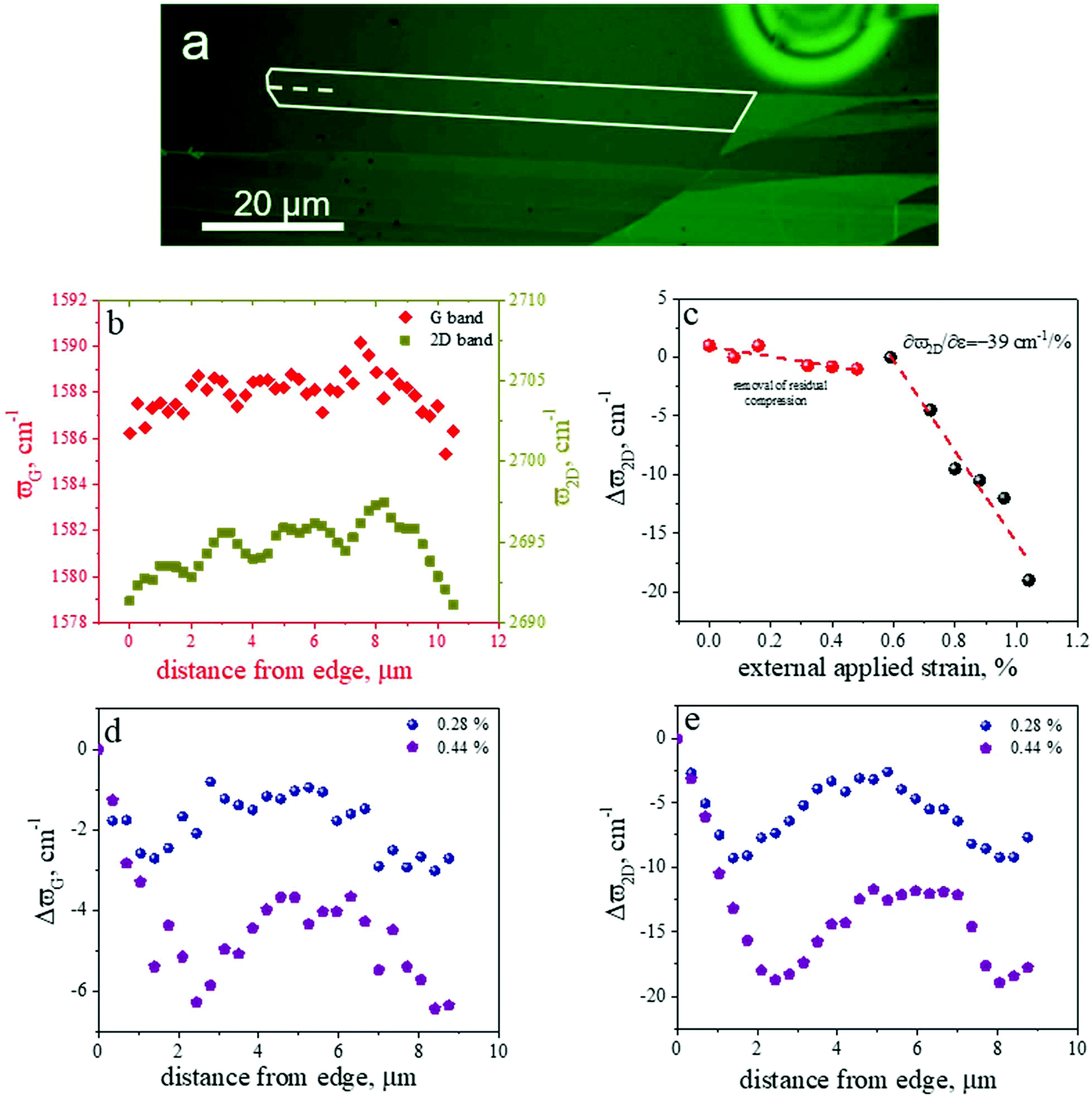 | ||
| Fig. 2 (a) Optical micrograph of the fully embedded monolayer graphene ribbon. The perimeter of the ribbon has been delimited to ease the visualization and the direction of Raman sampling is indicated as a dotted line. (b) The distributions of ωG and ω2D along the mapping line at the left-hand end of the ribbon at rest highlights an initial non-uniform, compressive, strain distribution (c) 2D peak position for spectra acquired far away from the edge as a function of applied strain. Two regions are marked: (i) flat region corresponding to the unfolding of the pre-existing wrinkles of the inclusion, (ii) linear region where graphene experiences axial tensile load. Raman shift of ωG (d) and ω2D (e) along the mapping line at two strain levels. | ||
As the material is loaded in tension by flexing the beam using a 4-point bending configuration, the external strain applied to graphene can be found either by the beam formula9 or by employing a strain gauge at the vicinity of the specimen. The fitted position of the 2D peak for spectra acquired far away from the left-hand edge is shown in Fig. 2c, as a function of applied stain evaluated using the beam formula. It is interesting to note that, for the system at hand, ω2D shifts at a low strain rate or forms a plateau up to applied strain 0.60%, then it shifts to lower wavenumbers with a slope of around 39 cm−1/%. The reason is that the graphene microribbon has been subjected to high compressive strains by the transfer process and the polymer solidification and we assume that it has failed in axial compression. The threshold for applied strain for compressive failure has been identified to be −0.6%.28 It is therefore not surprising that in order to impart a tensile deformation to the ribbon we need to take out the residual compressive strain. Hence, two regions can be distinguished: a plateau region, where no appreciable shift is detected corresponding to the takeover of the compressive strain, and a linear region in which graphene ribbon is subjected to an axial tensile load. A proof for that is that the specimen has been unloaded and loaded again and as seen in Fig. S2† identical results have been obtained (ESI†). In light of Fig. 2c at 0.6%, we assume that this is the actual zero-point deformation of the investigated graphene micro-ribbon.
The experimental data of the 2D and G peaks shift as a function of distance from the free end, are plotted in Fig. 2d and e for various increments of tensile strains. Representative Raman spectra at different applied strain levels are presented also in Fig. S1.† As the material is loaded in tension, systematic shifts of the peaks are obtained as one moves from the edge of the ribbon towards the middle as a result of stress transfer from the surrounding PMMA to graphene across the interface.
To estimate the real strain applied to the graphene ribbon, the exact ω2D peak value of the graphene at 0.0% of applied strain should be known. In this case, we consider the weighted average of ω2D values of all the data points along the mapping line that were located within the region from 2 to 4 μm as a representative ω2D value in the absence of external loading. This is found be 2694.4 ± 1.8 cm−1. Then using the ω2D at each mapping point, the corresponding strain, ε, was estimated from the following relationship:18
 | (1) |
In Fig. 3a and b, the fitted shifts of 2D and G peaks, as presented in Fig. 2d and e, are converted to strain distributions along the left-hand edge of graphene ribbon according to the procedure reported above. As seen, the distribution of strains builds from a value of zero at the edge and then forms a plateau in analogy with the classic case of a single discontinuous fibre in a model composite.12 This picture of strain distribution is observed for the first time in graphene model nanocomposite and is due essentially to the combination of several important experimental parameters, such as the regular geometry of the sample, the accurate alignment of the micro-ribbon to the strain axis and the detailed observation of the edges. For both the axial strain distributions, a small deviation from the mean plateau value is observed in the range 2.5–7.5 μm (red symbols, Fig. 3a and b). This could be attributed to the presence of ripples due to the residual compression occurred upon the transfer process and the polymer solidification.
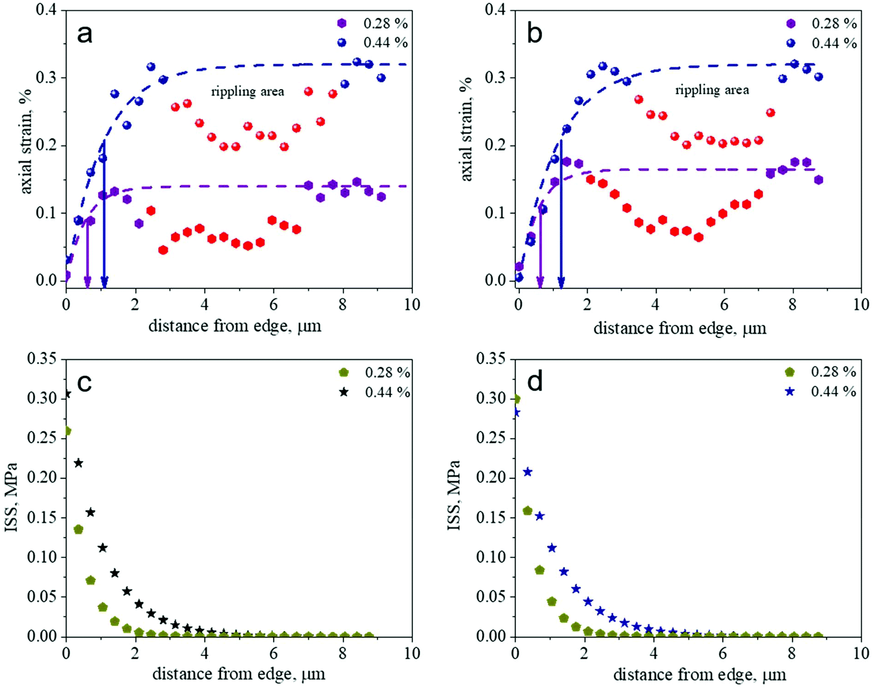 | ||
| Fig. 3 Axial strain profiles for two strain levels derived from the Raman wavenumber distributions of G (a) and 2D (b) peaks. The dotted line represents the fitting of the experimental data to eqn (2). The undulations observed correspond to the presence of low intensity ripples along the length of the inclusion and the arrows indicate the transfer length (lo) for each strain level. The corresponding interfacial shear stress distributions along the mapping line (c and d) have been evaluated from the balance of forces applied, respectively, to G and 2D strain profiles. | ||
Uniaxial stress in the substrate leads to the development of interfacial shear between graphene and polymer, which is, in turn, converted into a normal stress in the flake. This force transmitted through shear across the flake/substrate interface is acting primarily near the edges of the ribbon. Since the stress (strain) is transferred through shear we can use the balance of forces equation (ESI†) which for the simply supported case is given by:
 | (2) |
In general, the geometry and the location of the flakes obtained via micromechanical cleavage cannot be controlled; therefore, transfer methods have been developed in order to allow controlled placement of flakes on specific locations of substrates for practical applications. In order to verify if the transfer process and thus the presence of these corrugations may affect the strain build-up, an embedded 1LG ribbon obtained from mechanical exfoliation directly on a PMMA bar was also examined. As shown in Fig. 4, similar stress transfer results were obtained from the 1LG ribbon produced from direct mechanical exfoliation. In particular, transfer lengths of 400 nm to 1 μm have been measured at different applied strains, which are close to those obtained for the ribbons placed on PMMA bar via wet transfer. We conclude therefore that the presence of rippling at a distance from the graphene edge does not affect significantly the stress transfer characteristics in the studied material system.
 | ||
| Fig. 4 Optical micrograph of the fully embedded 1LG ribbon obtained via direct exfoliation on the PMMA bar and consequent spin coating (a). The distribution of ω2D along the mapping line at the left-hand end of the ribbon at rest highlights an initial non-uniform, compressive, strain distribution (b); axial strain profiles for three strain levels derived from the Raman wavenumber distributions of 2D peaks (c). | ||
We can now provide a model for the prediction of the axial strain distribution which is based on the modification of the shear lag analysis performed earlier on composite systems involving fibers11 or flakes9 of micrometre dimensions embedded into a glassy polymer. As presented in ESI† for the case of a rectangular graphene monolayer the normal stress or strain functions built from the ends can be given by:
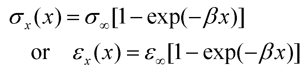 | (3) |
| Strain (%) | β (10−3 nm−1) | 1/β = lo (nm) | (Gm,T)/(T/2) (MPa nm−1) | |||
|---|---|---|---|---|---|---|
| 2D peak | G peak | 2D peak | G peak | 2D peak | G peak | |
| 0.28 | 1.816 | 1.853 | 550 | 540 | 0.55 | 0.57 |
| 0.44 | 0.885 | 0.957 | 1100 | 1050 | 0.13 | 0.15 |
Another way to estimate the value of β is through the modified shear lag analysis (see ESI†) in which β is found to be related to the elastic moduli of the material involved and the geometry of the problem. As shown (ESI†), one can easily produce a universal analytical formula for this parameter which is given by:
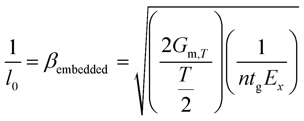 | (4) |
In fact the value of the square root is governed by the product of two terms; an interphase term which involves the shear modulus at the interface, Gm,T and the thickness T of the polymer layer that surrounds the inclusion32 and a second term that refers to the size and elastic modulus of the nano-inclusion (here graphene of n layers). By putting n = 1, tg = 0.335 nm and Ex = 1 TPa into eqn (4) we get:
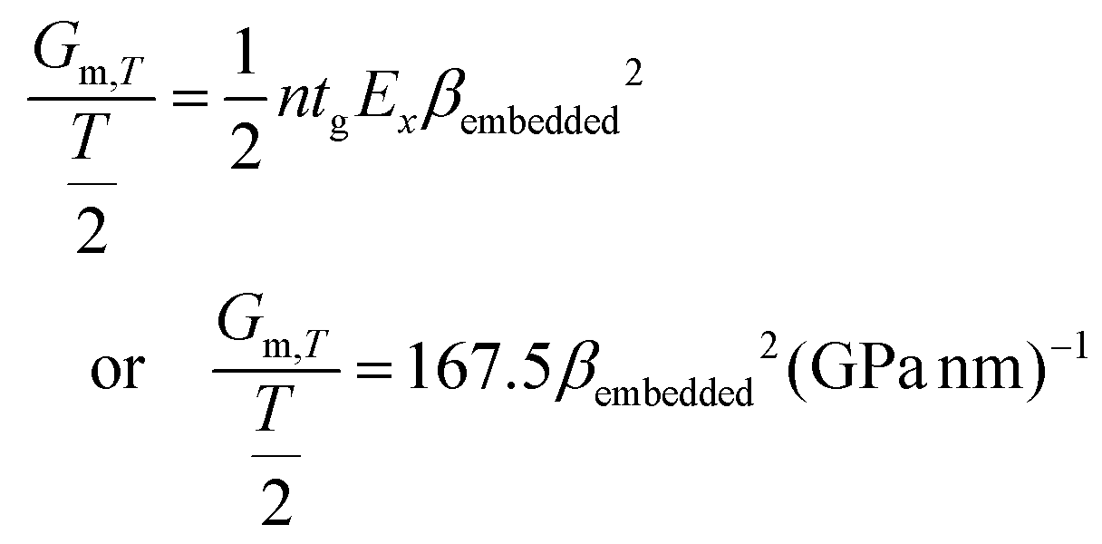 | (5) |
The values of the interphase parameter (Gm,T/T/2) for all the strain profiles calculated through eqn (5) are also given in Table 1. As mentioned above in order to estimate the interphase parameter from the knowledge of the interface properties, we need to know the values of both T and Gm,T near graphene. The bulk shear modulus of PMMA is approximately 550 MPa but its exact value near the surface at the graphene location is not known although since there is no primary chemical bonding developed between polymer and graphene this value should be a good estimate. The value of T is also difficult to define accurately; most workers in the field of composite micromechanics consider T as the thickness of the surrounding matrix, which is not strictly appropriate since T should be defined at the point where the matrix deforms freely (i.e. exhibits no shear-lag effect). In this case for which the inclusion is near the surface of a beam the half size of the zone of influence cannot be higher that T/2 which is the distance between the inclusion and the polymer free surface. Thus, if we put T/2 ≥ 300 nm, which is approximately the thickness of the PMMA transfer layer and Gm,T = 550 MPa (PMMA bulk modulus), then we obtain 1/β ≥ 320 nm which is close enough to the values obtained experimentally (Table 1) through the fitting of the raw data with the exponential functions of eqn (3). The broad agreement between the transfer length values l0 obtained by fitting the experimental data and those derived from theory is indeed remarkable if we consider the simplicity of the shear-lag analysis pursued here (ESI†). This conformity to the axial loading results from the regular geometry of the ribbon that ensures normal stress transfer and no orthogonal buckling that is usually induced to irregular flakes by the Poisson's contraction of the surrounding matrix. It is worth noting there that the above-presented modified shear lag analysis for graphene also takes into account the increase of transfer length with the increase of applied strain (Table 1) as expected from the decrease of the polymer shear modulus with strain which results from the gradual onset of polymer yielding.32 Moreover, our analysis considers the flake as having a rectangular shape which is applicable also to micro-ribbons geometries or in other words for cases that conform to w ≪ l. This finding is of paramount importance since for specific shapes the transfer length is around 1 μm as predicted from the modified shear lag analysis presented here.
Conclusions
In conclusion, we have investigated the stress transfer characteristics along graphene micro-ribbon aligned to the loading direction. This ensured truly axial deformation and avoidance of off-axis shear or lateral buckling effects that could affect the stress transfer mechanism. Moreover, by modifying the classical shear-lag model,11,33 we derived an inverse length parameter that governs fully the stress transfer process and all relevant interface parameters (e.g. transfer length, maximum interfacial shear strength etc.). The results obtained revealed that – in contrast to previously reported7 – the transfer lengths in flakes of monoatomic thickness depend on the applied strain and range from 500 to 1000 nm. Finally, by considering a simple balance of shear-to-axial forces a maximum value of shear stress of approximately 0.3 MPa is obtained at 0.42% strain on graphene flake which conforms well to the nature of bonding between graphene and polymer substrate.Experimental
The PMMA-embedded graphene micro-ribbon was prepared by wet transfer of a previously mechanically exfoliated graphene. Firstly, graphene flakes were produced by mechanical exfoliation of graphite using ‘scotch’ tape technique.34 Then the tape was glued onto a three-layer substrate made up of PMMA (at the top), PMGI (in the middle), and silicon (at the bottom). After, by removing the tape, graphene/graphite flakes have been transferred on the substrate, and single-layer graphene ribbon was identified based on its contrast.35 The middle layer (PMGI) was dissolved using a specific solvent, without affecting the PMMA layer on top. As a result, the graphene–PMMA system was floating on the solution bath and the PMMA membrane was then picked up and inverted onto a PMMA beam of 3 mm thickness by using a micromanipulator. Finally, in order to aid adhesion, the sample has been heated at 130 °C. Specimen from direct exfoliation on the PMMA bar were also produced. In this case, after identification of single-layer graphene ribbon, the substrate was adequately cut in order to ensure the alignment of the ribbon along the longitudinal axis of the bar. Finally, the ribbon was embedded by consequent spin coating a thin film of PMMA of thickness of 150 nm ca.In both the samples, the thickness of the PMMA substrate was t = 3.0 mm and the investigated ribbon was located at a distance, L/2, where L = 80 mm is the length of the supporting span of a four-point bending apparatus frame.
The top surface of each beam was subjected to tension by flexing upward the beam by means of an adjustable screw. The deflection δ was achieved by rotating a small lever connected to a set of gears and a long screw attached to the moving jaw of the four-point bending apparatus. Slow traveling of the lever results in accurate incremental steps of applied strains to the specimens. The strain direction was approximately parallel (2 degrees from the horizontal axis) to the longitudinal axis of the ribbon. The actual strain in graphene flake was evaluated from the analysis of the Raman spectra acquired from the middle of the ribbon, according to the well-established method proposed by Frank et al.18 Small differences from the strain applied from the 4-point bending device are due to the graphene transfer procedure.
The four-point bending frame was placed above the High Speed Encoded Stage of the Micro-Raman (InVia Reflex, Renishaw, UK) spectrograph. At each deflection level the stage was moved every 350 nm collecting simultaneously Raman spectra, allowing to perform a detailed mapping across a specific line (as indicated in Fig. 2) on the flake. Raman spectra are measured at 514 nm (1.58 eV) and the laser power was kept at 1.2 mW on the sample to avoid laser-induced local heating. A 100× objective with numerical aperture of 0.95 is used, and the spot size was estimated 0.8 μm2. The polarization of the incident light was kept parallel to the applied strain axis. All Raman spectra were fitted with Lorentzians.
Conflicts of interest
The authors would like to declare no conflicts of interests.Acknowledgements
The authors acknowledge the financial support of the European Research Council (ERC Advanced Grant 2013) via project no. 321124, “Tailor Graphene” and the Open FET project “Development of continuous two-dimensional defect-free materials by liquid-metal catalytic routes” no. 736299-LMCat which is implemented under the EU-Horizon 2020 Research Executive Agency (REA) and is financially supported by EC.Notes and references
- K. S. Novoselov, V. I. Fal'ko, L. Colombo, P. R. Gellert, M. G. Schwab and K. Kim, Nature, 2012, 490, 192–200 CrossRef CAS PubMed.
- C. Lee, X. D. Wei, J. W. Kysar and J. Hone, Science, 2008, 321, 385–388 CrossRef CAS PubMed.
- J. Kang, D. Shin, S. Bae and B. H. Hong, Nanoscale, 2012, 4, 5527–5537 RSC.
- G. D. Guo and Y. Zhu, J. Appl. Mech., 2015, 82 Search PubMed.
- I. Polyzos, M. Bianchi, L. Rizzi, E. N. Koukaras, J. Parthenios, K. Papagelis, R. Sordan and C. Galiotis, Nanoscale, 2015, 7, 13033–13042 RSC.
- M. G. P. Carbone, A. C. Manikas, I. Souli, C. Pavlou and C. Galiotis, Nat. Commun., 2019, 10, 7 CrossRef PubMed.
- L. Gong, I. A. Kinloch, R. J. Young, I. Riaz, R. Jalil and K. S. Novoselov, Adv. Mater., 2010, 22, 2694–2697 CrossRef CAS PubMed.
- L. Gong, R. J. Young, I. A. Kinloch, I. Riaz, R. Jalil and K. S. Novoselov, ACS Nano, 2012, 6, 2086–2095 CrossRef CAS PubMed.
- G. Anagnostopoulos, C. Androulidakis, E. N. Koukaras, G. Tsoukleri, I. Polyzos, J. Parthenios, K. Papagelis and C. Galiotis, ACS Appl. Mater. Interfaces, 2015, 7, 4216–4223 CrossRef CAS PubMed.
- G. Wang, Z. Dai, L. Liu, H. Hu, Q. Dai and Z. Zhang, ACS Appl. Mater. Interfaces, 2016, 22554–25562 CrossRef CAS PubMed.
- C. Galiotis and A. Paipetis, J. Mater. Sci., 1998, 33, 1137–1143 CrossRef CAS.
- N. Melanitis, C. Galiotis, P. L. Tetlow and C. K. L. Davies, J. Compos. Mater., 1992, 26, 574–610 CrossRef CAS.
- L. S. Schadler, S. C. Giannaris and P. M. Ajayan, Appl. Phys. Lett., 1998, 73, 3842–3844 CrossRef CAS.
- S. Piscanec, M. Lazzeri, J. Robertson, A. C. Ferrari and F. Mauri, Phys. Rev. B: Condens. Matter Mater. Phys., 2007, 75, 22 CrossRef.
- A. C. Ferrari and J. Robertson, Philos. Trans. R. Soc. London, Ser. A, 2004, 362, 2269–2270 CrossRef.
- S. B. Cronin, A. K. Swan, M. S. Unlu, B. B. Goldberg, M. S. Dresselhaus and M. Tinkham, Phys. Rev. Lett., 2004, 93, 4 CrossRef PubMed.
- S. B. Cronin, A. K. Swan, M. S. Unlu, B. B. Goldberg, M. S. Dresselhaus and M. Tinkham, Phys. Rev. B: Condens. Matter Mater. Phys., 2005, 72, 8 CrossRef.
- O. Frank, G. Tsoukleri, I. Riaz, K. Papagelis, J. Parthenios, A. C. Ferrari, A. K. Geim, K. S. Novoselov and C. Galiotis, Nat. Commun., 2011, 2, 7 Search PubMed.
- T. M. G. Mohiuddin, A. Lombardo, R. R. Nair, A. Bonetti, G. Savini, R. Jalil, N. Bonini, D. M. Basko, C. Galiotis, N. Marzari, K. S. Novoselov, A. K. Geim and A. C. Ferrari, Phys. Rev. B: Condens. Matter Mater. Phys., 2009, 79, 8 CrossRef.
- T. Jiang, R. Huang and Y. Zhu, Adv. Funct. Mater., 2014, 24, 396–402 CrossRef CAS.
- F. J. G. de Abajo, ACS Photonics, 2014, 1, 135–152 CrossRef.
- R. Alaee, M. Farhat, C. Rockstuhl and F. Lederer, Opt. Express, 2012, 20, 28017–28024 CrossRef CAS PubMed.
- H. Tian, Y. Shu, Y. L. Cui, W. T. Mi, Y. Yang, D. Xie and T. L. Ren, Nanoscale, 2014, 6, 699–705 RSC.
- A. Salehi-Khojin, D. Estrada, K. Y. Lin, M. H. Bae, F. Xiong, E. Pop and R. I. Masel, Adv. Mater., 2012, 24, 53–57 CrossRef CAS PubMed.
- Z. Q. Niu, L. Zhang, L. Liu, B. W. Zhu, H. B. Dong and X. D. Chen, Adv. Mater., 2013, 25, 4035–4042 CrossRef CAS PubMed.
- A. Reina, H. B. Son, L. Y. Jiao, B. Fan, M. S. Dresselhaus, Z. F. Liu and J. Kong, J. Phys. Chem. C, 2008, 112, 17741–17744 CrossRef CAS.
- A. C. Ferrari and D. M. Basko, Nat. Nanotechnol., 2013, 8, 235–246 CrossRef CAS PubMed.
- C. Androulidakis, E. N. Koukaras, O. Frank, G. Tsoukleri, D. Sfyris, J. Parthenios, N. Pugno, K. Papagelis, K. S. Novoselov and C. Galiotis, Sci. Rep., 2014, 4, 8 Search PubMed.
- O. Frank, M. Mohr, J. Maultzsch, C. Thomsen, I. Riaz, R. Jalil, K. S. Novoselov, G. Tsoukleri, J. Parthenios, K. Papagelis, L. Kavan and C. Galiotis, ACS Nano, 2011, 5, 2231–2239 CrossRef CAS PubMed.
- D. Yoon, Y. W. Son and H. Cheong, Phys. Rev. Lett., 2011, 106, 4 Search PubMed.
- M. Y. Huang, H. G. Yan, T. F. Heinz and J. Hone, Nano Lett., 2010, 10, 4074–4079 CrossRef CAS PubMed.
- G. Anagnostopoulos, J. Parthenios, A. G. Andreopoulos and C. Galiotis, Acta Mater., 2005, 53, 4173–4183 CrossRef CAS.
- H. L. Cox, Br. J. Appl. Phys., 1952, 3, 72–79 CrossRef.
- K. S. Novoselov, A. K. Geim, S. V. Morozov, D. Jiang, Y. Zhang, S. V. Dubonos, I. V. Grigorieva and A. A. Firsov, Science, 2004, 306, 666–669 CrossRef CAS PubMed.
- P. Blake, E. W. Hill, A. H. Castro Neto, K. S. Novoselov, D. Jiang, R. Yang, T. J. Booth and A. K. Geim, Appl. Phys. Lett., 2007, 91, 3 CrossRef.
Footnote |
| † Electronic supplementary information (ESI) available. See DOI: 10.1039/c9nr03166a |
| This journal is © The Royal Society of Chemistry 2019 |