
Tailoring Ti3C2Tx nanosheets to tune local conductive network as an environmentally friendly material for highly efficient electromagnetic interference shielding†
Peng
He
a,
Xi-Xi
Wang
a,
Yong-Zhu
Cai
a,
Jin-Cheng
Shu
a,
Quan-Liang
Zhao
b,
Jie
Yuan
c and
Mao-Sheng
Cao
 *a
*a
aSchool of Materials Science and Engineering, Beijing Institute of Technology, Beijing, 100081, China. E-mail: caomaosheng@bit.edu.cn
bSchool of Mechanical and Material Engineering, North China University of Technology, Beijing, 100144, China
cSchool of Information Engineering, Minzu University of China, Beijing, 100081, China
First published on 27th February 2019
Abstract
Environmentally friendly materials that exhibit high-performance electromagnetic interference (EMI) shielding are extremely necessary. Herein, we fabricated ultrathin Ti3C2Tx (U-Ti3C2Tx) MXene nanosheets (NS) by atomic-layer tailoring the layer thickness of Ti3C2Tx MXene. The U-Ti3C2Tx NS composites with highly efficient EMI shielding effectiveness can reduce secondary reflection, demonstrating its environmentally friendly performance. The U-Ti3C2Tx NS composite with 80 wt% loading exhibits an EMI shielding effectiveness of 58.1 dB at a thickness of 1 mm. Shielding performance analysis of different layer thicknesses shows that electron transport has an important contribution to the EMI shielding performance. Furthermore, the polarization induced by defects and terminal atoms plays an important role in the EMI shielding performance. Based on the electromagnetic (EM) wave response mechanism, a novel approach to effectively tune the EMI attenuation and shielding effectiveness can be achieved by adjusting the local conductive network. These findings will offer an effective strategy for designing environmentally friendly 2D materials with high-performance EMI shielding.
Introduction
Electromagnetic (EM) radiation pollution has been severely increased with the rapid development of modern electronic technology.1–10 Particularly, EM radiation is a great hazard to human health, and long-term EM radiation can cause serious diseases such as leukemia and cancer. Therefore, the development of effective EM wave absorption and shielding materials has attracted more and more attention.11–33Two-dimensional (2D) materials are widely used as multi-functional materials due to their unusual electronic, mechanical, and optical properties. They also show excellent performances in EM wave absorption and shielding.34–41 MXene, a new member of 2D materials, was first prepared by high-concentration HF etching of Ti3AlC2.42 Typically, these materials can be written as Mn+1XnTx, where M denotes the transition metal, X represents C/N, and Tx is used to represent functional groups (![[double bond, length as m-dash]](https://www.rsc.org/images/entities/char_e001.gif) O, –OH and –F).43 As a new 2D material, MXenes with high metallic conductivities and hydrophilic surfaces exhibit excellent performances in energy storage,43–47 sewage purification,48 electrocatalysis,49 photoelectric transmission,50 and many other applications.51 For example, Jiang et al. reported that a pseudocapacitance-dominated MoS2-in-Ti3C2 superstructure exhibits a highly reversible Li+ storage capacity.52
O, –OH and –F).43 As a new 2D material, MXenes with high metallic conductivities and hydrophilic surfaces exhibit excellent performances in energy storage,43–47 sewage purification,48 electrocatalysis,49 photoelectric transmission,50 and many other applications.51 For example, Jiang et al. reported that a pseudocapacitance-dominated MoS2-in-Ti3C2 superstructure exhibits a highly reversible Li+ storage capacity.52
Moreover, researchers are gradually becoming interested in the EM wave absorption and shielding characteristics of MXenes. Initially, Gogotsi et al. prepared a 45 μm Ti3C2Tx film exhibiting an electromagnetic interference (EMI) shielding effectiveness (SE) of 92 dB, which is the highest among fabricated materials prepared heretofore.53 Simultaneously, a series of studies on modified Mxenes reported by Yin et al. shows that modified Mxenes exhibited high EM wave absorption and shielding properties.54–57 Subsequently, Yu et al. fabricated lightweight, hydrophobic, and flexible MXene foams, where MXene foams exhibited excellent performance in EMI shielding.58 Additional researches describing the EM wave absorption and shielding performance of MXene have been reported.59–71 In conclusion, MXenes have become rising stars showing potential advantages in the field of EM wave absorption and shielding. However, the investigation of the EM wave shielding performances of MXenes is still in the exploratory stage, and the realization of strong absorption and low secondary reflection for high-performance EMI shielding effectiveness is still a challenge.
In this paper, ultrathin Ti3C2Tx (U-Ti3C2Tx) MXene nanosheets (NS) were successfully fabricated by a modified Gogotsi's method. The formation mechanism of U-Ti3C2Tx MXene NS is illustrated. The electromagnetic properties of Ti3C2Tx MXenes based on different layer thicknesses were systematically investigated. The roles of electron transport and local conductive network in the EMI shielding performance of Ti3C2Tx MXenes are revealed in detail. Notably, the important roles of defects and terminal atoms in EMI shielding performance were systematically analyzed. More significantly, by atomic layer tailoring (ALT) the layer thickness of Ti3C2Tx MXenes to induce the formation of local conductive network, a high-performance EMI shielding U-Ti3C2Tx MXene NS composite was obtained that could effectively reduce secondary reflection illustrating its environmentally friendly performance.
Experimental
Experimental materials
Ti3AlC2 powders (purity >98%, ∼300 mesh) were provided by Lianlixin Technology Ltd (Beijing, China). Lithium fluoride (LiF) was supplied by Macklin Technology Ltd (Shanghai, China). Hydrochloric acid (HCl) (35 wt%) and hydrofluoric acid (HF) (40 wt%) were supplied by Beijing Chemical Factory (Beijing, China). All the chemicals were used without further purification.Preparation of multilayered Ti3C2Tx MXenes
Multilayered Ti3C2Tx (M-Ti3C2Tx) MXenes were synthesized by etching a Ti3AlC2 phase with HF as previously reported.72 1 g Ti3AlC2 was added into a 20 mL HF solution (40 wt%) and was stirred at room temperature for 24 h. After this reaction, the resultant product was repeatedly washed with deionized water and centrifuged at 3500 rpm until an almost neutral pH (≥6) was reached. Then, the supernatant, which is a colloidal solution of M-Ti3C2Tx, was gathered. Finally, the colloidal solutions were filtered through a membrane and dried in a desiccator under vacuum at room temperature.Preparation of ultrathin Ti3C2Tx MXenes
Ultrathin Ti3C2Tx (U-Ti3C2Tx) MXenes were prepared by using a modified Gogotsi's method. 1 g of LiF was added into 20 mL of 6 M HCl and the contents were allowed to mix completely for 5 minutes at room temperature. Then, 1 g of Ti3AlC2 was immersed in the mixture and stirred at 40 °C for 16 h. After this reaction, the resultant product was repeatedly washed with deionized water and centrifuged at 3500 rpm until an almost neutral pH (≥6) was reached. After that, the supernatant, which is the colloidal solution of U-Ti3C2Tx nanosheets (NS), was gathered. Finally, the colloidal solutions were filtered through a membrane and dried in a desiccator under vacuum at room temperature.Preparation of samples
In a typical experiment, the M-Ti3C2Tx MXenes (20, 40, 60, 80 wt% loading) were mixed with SiO2 nanopowders. SiO2 is an EM wave transparent material and is used as the matrix. SiO2 powder was mixed with M-Ti3C2Tx and ground into ultrafine grains. Then, the mixed powders were cold-pressed into rectangular-shaped samples with dimensions of 22.86 mm × 10.16 mm × 1 mm under a pressure of 5 MPa. Similarly, the preparation of U-Ti3C2Tx/SiO2 (20, 40, 60, 80 wt% loading) follows the same procedure as described above.Characterization
X-ray diffraction (XRD) was measured on an X'Pert PRO system (Cu Kα). X-ray photoelectron spectroscopy (XPS) measurements were performed by a PHI Quantera system. Scanning electron microscopy (SEM) images were obtained on a scanning electron microscope system (SEM Hitachi S-4800). Atomic force microscopy (AFM) images were obtained on a Veeco Dimension Fast Scan system. Transmission electron microscopy (TEM) images were collected by a TEM-2100F microscope. The S parameters of samples were measured by using a wave guide method with a vector network analyzer (VNA Anritsu 37269D) in the X-band region. Meanwhile, their DC conductivities (σ) were measured by a Keithley 4200-SCS semiconductor characterization system.Results and discussion
Factors affecting layer thickness of MXene
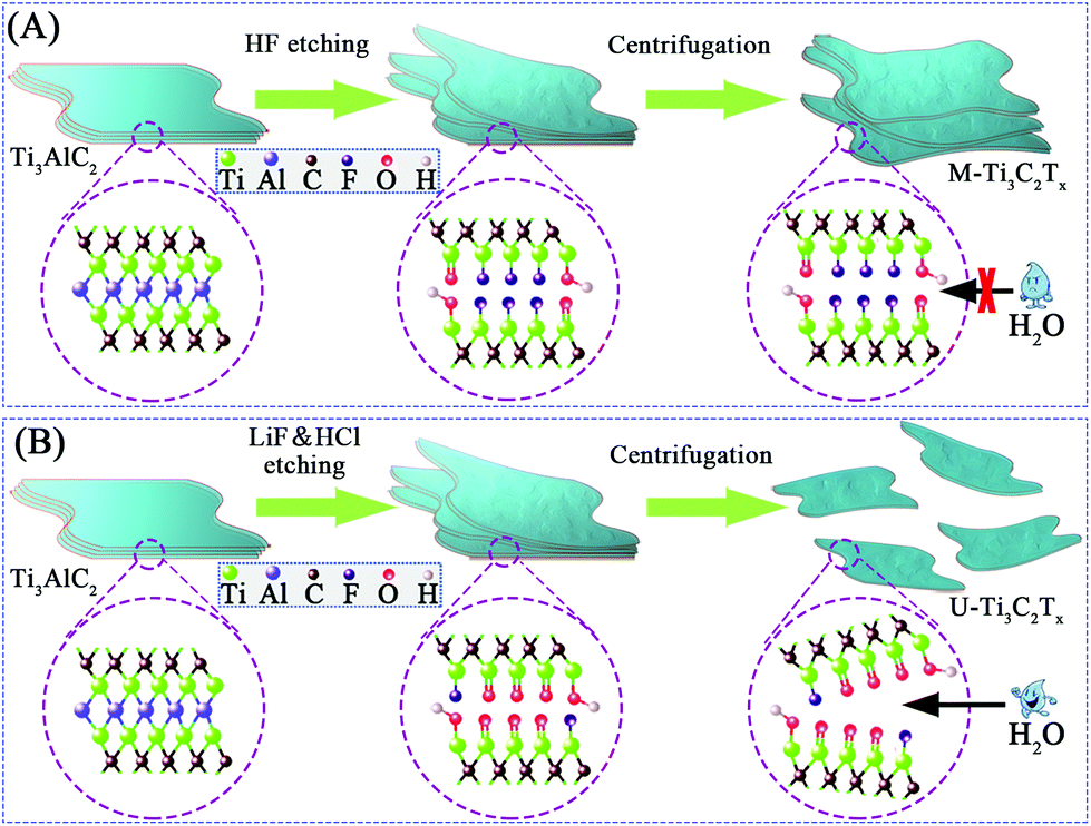
Fig. 1 explains the preparation of M-Ti3C2Tx and U-Ti3C2Tx MXenes. After centrifugation, Ti3AlC2 that was etched by HF has a multilayered structure (referred to as “M-Ti3C2Tx”), while Ti3AlC2 that was etched by LiF/HCl can be separated into an ultrathin structure (referred to as “U-Ti3C2Tx”). These very different results may be due to the different surface functional groups in the etched samples.73,74 The content of –F terminal groups in M-Ti3C2Tx is high while the content ofO terminal groups in U-Ti3C2Tx is high.73 Additionally, during the LiF/HCl etching, the temperature was increased from 35 °C to 40 °C. The reaction time was shortened from 24 hours to 16 hours compared with the previous work,75 which could effectively improve the efficiency of producing U-Ti3C2Tx.
 | ||
| Fig. 1 Synthetic illustration of (A) M-Ti3C2Tx and (B) U-Ti3C2Tx MXenes. | ||
The different layered structures of MXenes fabricated by two distinct methods are displayed in the results of the powder XRD analysis. As shown in Fig. S1 (ESI†), there is a shift of the (002) peak of Ti3AlC2 at ∼9.5° to ∼6.0° in the diffraction patterns of M-Ti3C2Tx and U-Ti3C2Tx, which is ascribed to the elimination of the Al from Ti3AlC2. XPS is implemented to further investigate the surface environment and the oxidation states of MXenes. Fig. 2A and B show the survey spectra of the M-Ti3C2Tx and U-Ti3C2Tx. The four main elements on the surface of MXenes are F, C, O and Ti. Moreover, the illustrations of Fig. 2A and B show the Ti 2p spectra of M-Ti3C2Tx and U-Ti3C2Tx. The signal labelled C-Ti-Tx 2p3/2 and 2p1/2 correspond to Ti interactions with terminal atoms and carbons. A slight increase in the intensity can be seen in the Ti 2p spectra of U-Ti3C2Tx at ∼459 and ∼465 eV compared with that of M-Ti3C2Tx in the same position (Fig. S2†). This can be further proved by the comparison of the component peak-fitting of XPS spectra for M-Ti3C2Tx and U-Ti3C2Tx Ti 2p at TiO2 2p3/2 (Fig. 2C) and TiO2 2p1/2 (Fig. 2D). These phenomena suggest that the oxidation degree of U-Ti3C2Tx is higher than that of M-Ti3C2Tx. According to the previous theoretical work, the area of U-Ti3C2Tx exposed to air is more than that of M-Ti3C2Tx, which will lead to faster oxidation.76
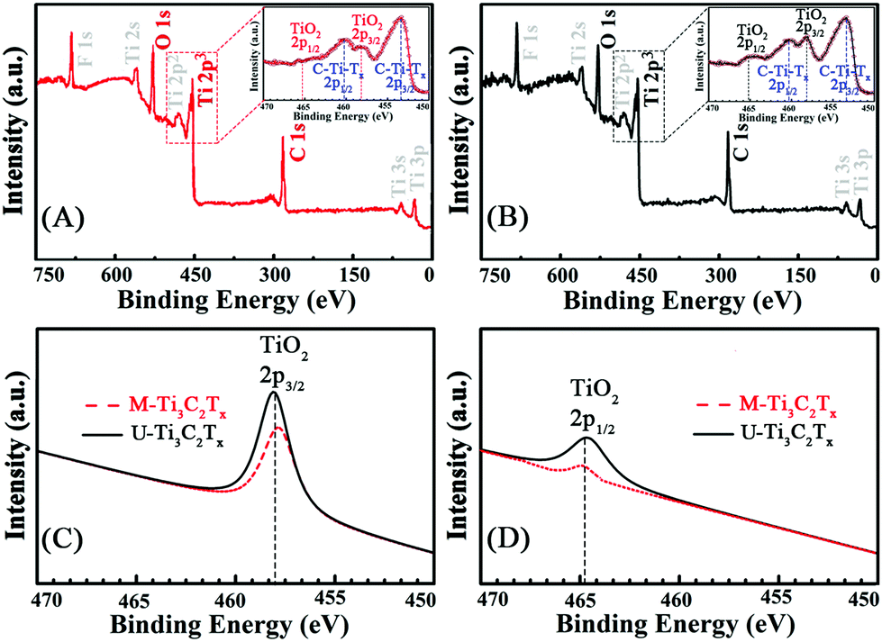 | ||
| Fig. 2 The survey spectra of (A) M-Ti3C2Tx and (B) U-Ti3C2Tx, high-resolution XPS for Ti 2p of M-Ti3C2Tx (inset in (A)) and U-Ti3C2Tx (inset in (B)). Comparison of component peak-fitting of XPS spectra for M-Ti3C2Tx and U-Ti3C2Tx Ti 2p at (C) TiO2 2p3/2 and (D) TiO2 2p1/2, where TiO2 2p3/2 and TiO2 2p1/2 represent the titanium in TiO2 that produces distinctive signals at ∼459 and ∼465 eV, respectively. | ||
The SEM images reveal the morphology of the M-Ti3C2Tx and U-Ti3C2Tx MXenes. As shown in Fig. 3C, the as-obtained M-Ti3C2Tx MXene has a typical multilayered morphology. It can clearly be seen that the M-Ti3C2Tx MXene has an accordion-like structure (Fig. 3D–F), and the average particle size is found to be ∼5 μm for the M-Ti3C2Tx MXene. The thickness of the U-Ti3C2Tx MXene is obviously thinner compared with that of the M-Ti3C2Tx MXene; the majority of the U-Ti3C2Tx MXene is of 1–4 μm in diameter (Fig. 3J–L). Above all, the SEM results demonstrate that the multilayered Ti3C2Tx MXene can be effectively separated into an ultrathin structure by ALT (Fig. 3A, B, G and H).
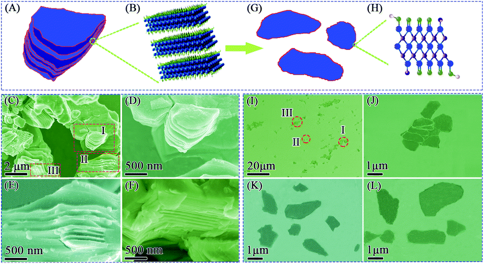 | ||
| Fig. 3 (A) Physical schematic of M-Ti3C2Tx. (B) The atomic schematic of M-Ti3C2Tx. (C) SEM image of M-Ti3C2Tx. (D)–(F) The high-magnification SEM image of M-Ti3C2Tx. (D), (E) and (F) correspond to the rectangle I, II and III in (C), respectively. (G) Physical schematic of U-Ti3C2Tx. (H) The atomic schematic of U-Ti3C2Tx. (I) SEM image of U-Ti3C2Tx. (J)–(L) The high-magnification SEM image of U-Ti3C2Tx. (J), (K) and (L) correspond to the circle I, II and III in (I), respectively. | ||
AFM was used to investigate the thicknesses and shapes of the M-Ti3C2Tx and U-Ti3C2Tx. As shown in Fig. 4A and B, the M-Ti3C2Tx shows an accordion-like structure. The formation of different interlayer distances (3.7 nm, 2.3 nm, 8.1 nm, 4.3 nm, as shown in Fig. 4D) was observed in the M-Ti3C2Tx MXenes based on the height profile measurement along the red dashed line in Fig. 4B. Additionally, Fig. 4C shows a 3D image of the M-Ti3C2Tx, further revealing that the M-Ti3C2Tx has an accordion-like structure. Fig. 4E–G show AFM images of the U-Ti3C2Tx. It can be clearly seen that the U-Ti3C2Tx MXenes have an average height of ∼2.6 nm, which is in accordance with the previous work.77 The results of AFM further confirm that U-Ti3C2Tx has an ultrathin structure.
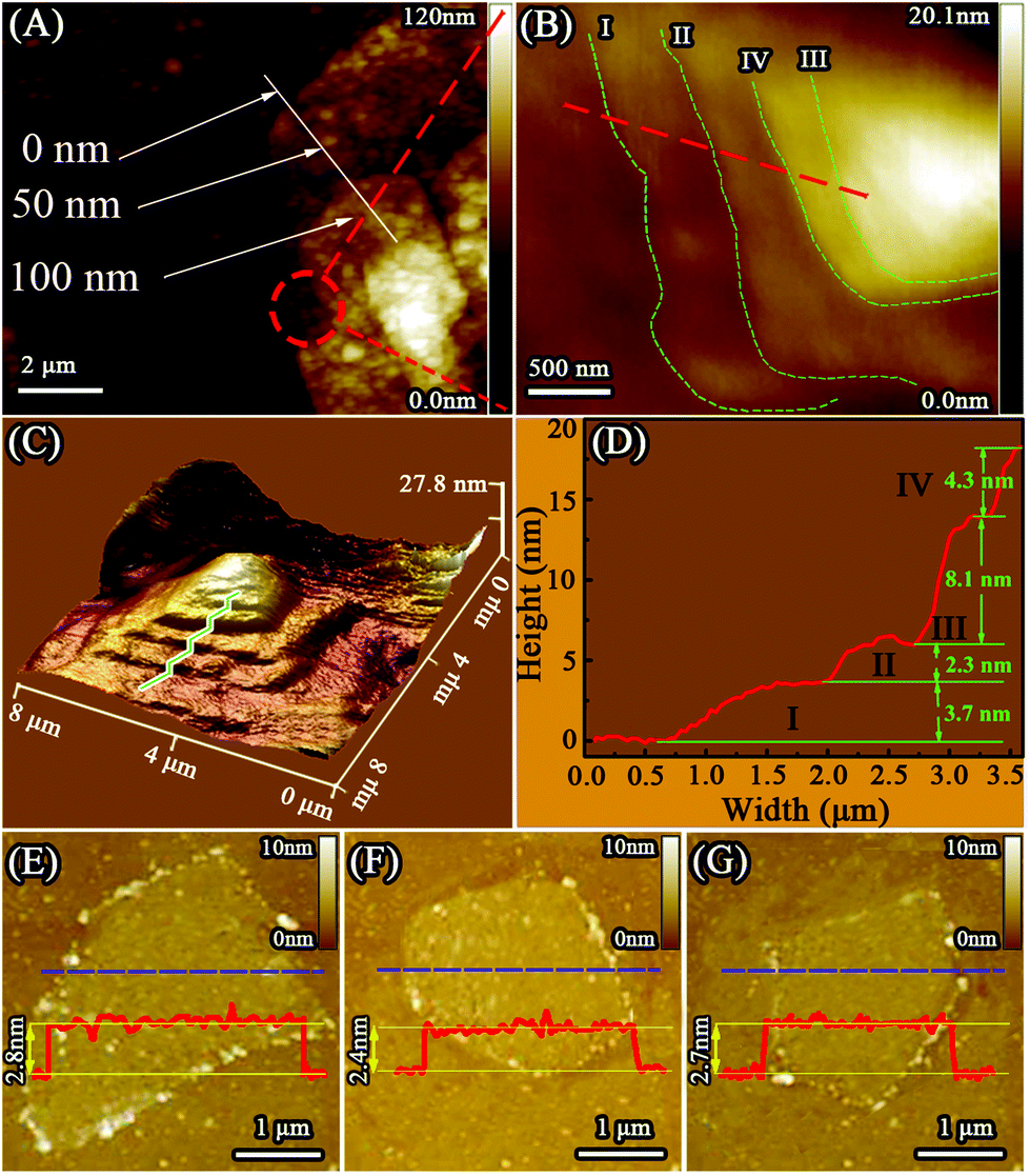 | ||
| Fig. 4 (A) and (B) AFM images of the M-Ti3C2Tx. (C) 3D images by AFM of the M-Ti3C2Tx corresponding to (B). (D) AFM height profile measured along the red dashed line in (B). (E)–(G) AFM images of the U-Ti3C2Tx. | ||
TEM was performed to further characterize the Ti3C2Tx MXenes fabricated by different methods. The M-Ti3C2Tx MXene has an accordion-like structure (Fig. 5A–D and Fig. S3A–D†), and the U-Ti3C2Tx MXene exhibits an ultrathin structure (Fig. 5G–J and Fig. S3E–H†), which are in accordance with the results of SEM (Fig. 3) and AFM (Fig. 4). High-resolution (HR) TEM images show a hexagonal arrangement of atoms in the plane (Fig. 5E and K), indicating that the crystal structures are the same for both MXenes, which is further corroborated by the selected area electron diffraction (SAED) patterns (Fig. 5F and L). However, the red dashed circle (Fig. 5F and Fig. S4A†) in the SAED pattern shows that there is a point of separation in the M-Ti3C2Tx MXene, which is different from the red dashed circle marked in the SAED pattern of U-Ti3C2Tx MXene (Fig. 5L and Fig. S4B†). This phenomenon is mainly due to the secondary diffraction caused by the multilayered structure of the M-Ti3C2Tx.
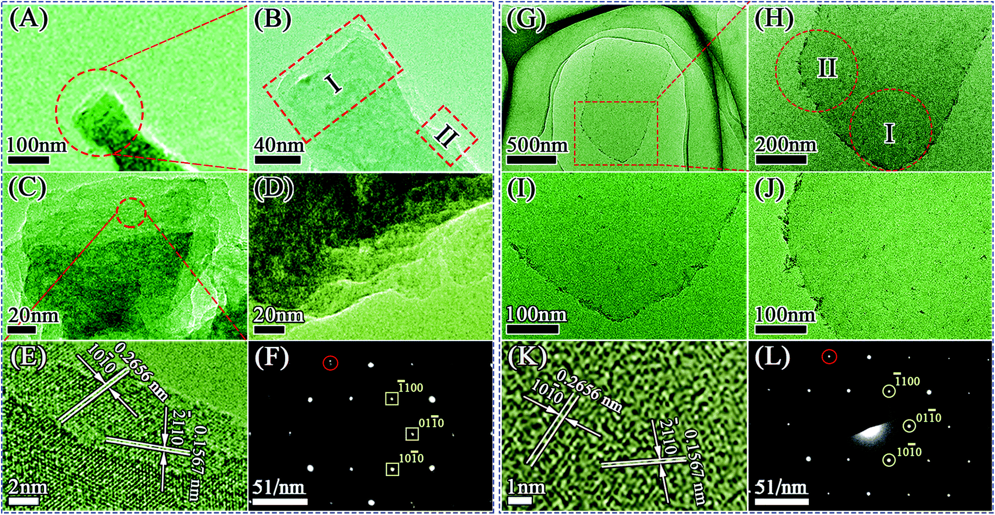 | ||
| Fig. 5 (A) TEM image of M-Ti3C2Tx. (B)–(D) The high-magnification TEM images of M-Ti3C2Tx. (C) and (D) correspond to the rectangle I and II in (B), respectively. (E) HRTEM image of M-Ti3C2Tx. (F) The SAED pattern of M-Ti3C2Tx. (G) TEM image of U-Ti3C2Tx. (H)–(J) The high-magnification TEM images of U-Ti3C2Tx. (I) and (J) correspond to the circle I and II in (H), respectively. (K) HRTEM image of U-Ti3C2Tx. (L) The SAED pattern of U-Ti3C2Tx. | ||
Fig. 6A–E show the atomic phase of U-Ti3C2Tx. It can be clearly seen that there are four kinds of vacancy defects on the surface of the U-Ti3C2Tx. Fig. 6F shows the generation of vacancy defects: one single Ti vacancy (VTi) and two VTi occurring within the same sub-layer; three VTi and two VTi occurring within two different sub-layers.78 Defects can only be formed at specific locations. These defects were formed during the etching process.78,79
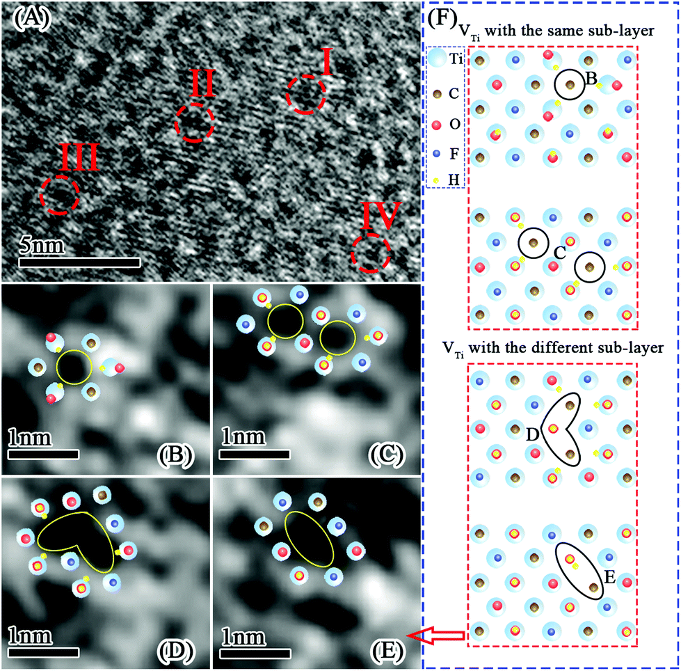 | ||
| Fig. 6 (A)–(E) Atomic phase of U-Ti3C2Tx. (B, C, D and E) correspond to the circle I, II, III and IV in (A), respectively. (F) Schematic illustration for defects generation: one single Ti vacancy (VTi) and two VTi occurring within the same sub-layer; three VTi and two VTi occurring within two different sub-layers. | ||
Effect of layer thickness on EMI shielding performance
For the purpose of investigating the EMI attenuation performances of the M-Ti3C2Tx and U-Ti3C2Tx composites, the scattering parameters (S11 and S21) were used to calculate the absorption (A), reflection (R), and transmission (T) coefficients of the M-Ti3C2Tx and U-Ti3C2Tx MXene composites.Fig. 7A and B show the absorption coefficients of the M-Ti3C2Tx and U-Ti3C2Tx. The absorption coefficients of the M-Ti3C2Tx and U-Ti3C2Tx NS composites achieve the maximum values of 0.21 and 0.26, respectively. Moreover, the maximum values of A for M-Ti3C2Tx and U-Ti3C2Tx are achieved in the composites with 60 wt% loading, which means that the maximum reflection loss (RL) is reached when the loading content of the M-Ti3C2Tx and U-Ti3C2Tx are 60 wt%, and this performance is due to good electromagnetic matching. Moreover, since the increased effective thickness of the composites with reducing wavelength, the A values of the M-Ti3C2Tx and U-Ti3C2Tx composites increase with the increase in the frequency (Fig. S5A–D†). Actually, a material absorbs EM waves and converts them into heat, and this conversion ability is determined by the conduction loss and the polarization loss. Polarization loss has an important contribution to the absorption of EM waves. In fact, the defects formed during the etching process (Fig. 6A–E) lead to the asymmetry in the spatial distribution of electrons to form dipole moments. Moreover, terminal atoms attached on the surface of MXenes (Fig. 2A and B) lead to the asymmetric distribution of charge density, which in-turn causes the formation of dipoles. Under an alternating electromagnetic field, these dipoles will break loose and rotate directionally. When their rotation cannot keep up with the change in electromagnetic field, polarization relaxation occurs with EM energy loss.12 Recent researches have mainly focused on the EMI shielding performance of Ti3C2Tx MXene films.53,58 However, EM waves are mostly reflected by high conductivity in the Ti3C2Tx film and this behavior is the same as a metal shielding the EM wave. Only a small amount of EM waves can enter the body of films and be absorbed. Compared with the MXene films that mainly use high conductivity to reflect EM waves, the composites made by dispersing the U-Ti3C2Tx MXene NS into the SiO2 matrix can reduce the conductivity and absorb more EM waves by polarization loss. This means that more EM waves can be attenuated so that secondary reflections will be effectively reduced, demonstrating their environmentally friendly performance.
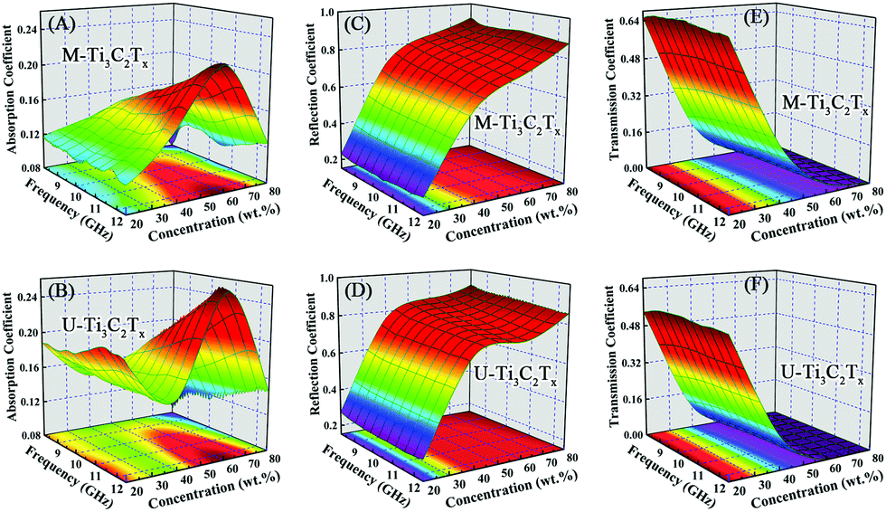 | ||
| Fig. 7 Absorption coefficients of (A) M-Ti3C2Tx and (B) U-Ti3C2Tx. Reflection coefficients of (C) M-Ti3C2Tx and (D) U-Ti3C2Tx. Transmission coefficients of (E) M-Ti3C2Tx and (F) U-Ti3C2Tx. | ||
Fig. 7C and D show the reflection coefficients of the M-Ti3C2Tx and U-Ti3C2Tx. The R values of both the M-Ti3C2Tx and U-Ti3C2Tx composites increase with the increase in mass ratio. This can be confirmed from the Fig. S5E–H.† The higher the concentration of Ti3C2Tx MXene is, the larger the conductivity will be. And this can cause more EM wave to be reflected. Meanwhile, the R values of the M-Ti3C2Tx and U-Ti3C2Tx composites decrease with an increase in the frequency, which is similar to the behavior of graphene. This may be due to the similar layer-structure.35,41
The transmission coefficients of the M-Ti3C2Tx and U-Ti3C2Tx are shown in Fig. 7E and F. An increase in the mass ratio for the M-Ti3C2Tx and U-Ti3C2Tx leads to a drastic abatement in the T values. Additionally, the T values of the U-Ti3C2Tx composite are less than those of the M-Ti3C2Tx composite (Fig. S5I–L†). The reason for this is that the high A and R values of the U-Ti3C2Tx composite lead to a remarkable decline in the T values, which means that more microwave radiation is shielded and absorbed by the U-Ti3C2Tx composite. This can be directly confirmed by the values of SEA and SER (Fig. S6†).
Analysis of EMI shielding mechanism
As a matter of fact, the EMI shielding efficiency (SE) of the material is often used to investigate the efficiency of the shielding materials, which is a judgement of the ability to dissipate EM wave. Based on the measured S parameters, the EMI SE can be obtained by:80,81EMISE = 10![[thin space (1/6-em)]](https://www.rsc.org/images/entities/char_2009.gif) log(PI/PT) = 10log(1/T), log(PI/PT) = 10log(1/T), | (1) |
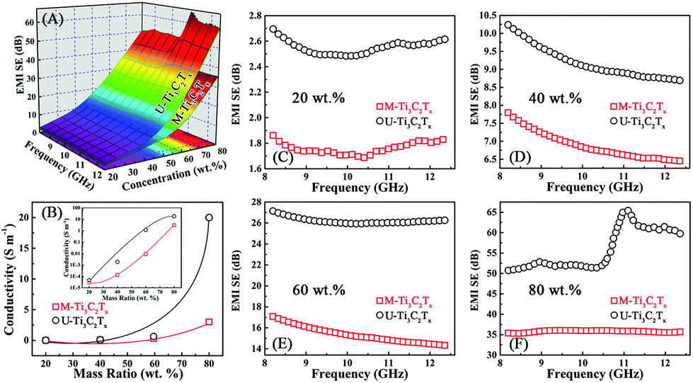 | ||
| Fig. 8 (A) EMI SE of the M-Ti3C2Tx and U-Ti3C2Tx composites. (B) DC conductivity (σ) vs. mass ratio of the M-Ti3C2Tx/SiO2 and U-Ti3C2Tx/SiO2 composites. The inset shows log10 DC conductivity (σ) vs. mass ratio. (C)–(F) EMI SE comparison of the M-Ti3C2Tx and U-Ti3C2Tx composites at each mass ratio. | ||
Regulation of local conductivity network
Usually, the conductivity of the Ti3C2Tx MXene composites is decided by the electronic mobility and formation of local conductive network. Herein, the electronic transport model and local conductive network theory are proposed to illustrate the EMI shielding performance of the M-Ti3C2Tx and U-Ti3C2Tx composites.As shown in Fig. 9A, the free electrons are uniformly distributed on the surfaces of U-Ti3C2Tx under electrostatic balance. These electrons do not collide with each other during transmission. In contrast, the electrons collide during transmission in the interlayer channels of M-Ti3C2Tx, which leads to the dropped electronic mobility showing reduced conductivity (Fig. 9B).82,83
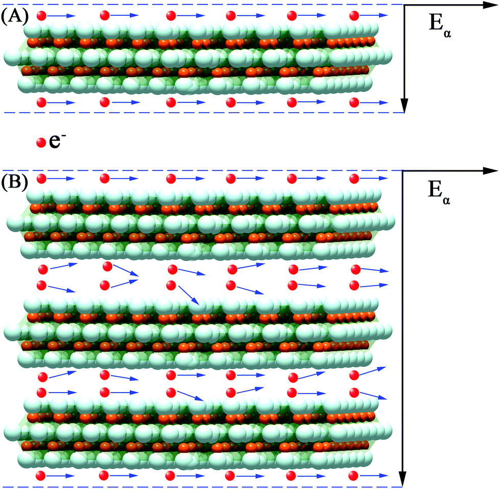 | ||
| Fig. 9 Schematic diagrams of the electronic transport channel and their scattering mechanisms for (A) U-Ti3C2Tx and (B) M-Ti3C2Tx. The Eα on the right represents the electric field distribution of U-Ti3C2Tx and M-Ti3C2Tx. | ||
Electronic transport has an important contribution to the conductivity of the pure material, whereas the formation of a local conductive network is more important for the conductivity in composites. Briefly, the local conductive network dominates the conductivity in composites. As shown in Fig. 10C, the electrons cannot jump between two layers of M-Ti3C2Tx MXenes when the distance between the layers of M-Ti3C2Tx MXenes gets larger. This leads to the failure in the formation of local conductive network in the M-Ti3C2Tx composites. Atomic layer tailoring the layer thickness of the Ti3C2Tx MXenes induces the formation of local conductive network (Fig. 10D). This leads to a much better shielding performance. As shown in Fig. 10E, the microwave has been further attenuated by multiple internal reflections in the M-Ti3C2Tx composite. The attenuation of microwaves through multiple scattering in the U-Ti3C2Tx composite is larger compared with that of the M-Ti3C2Tx composite (Fig. 10F). In brief, U-Ti3C2Tx MXene composites show a much better EMI shielding performance compared with the M-Ti3C2Tx MXene composites through the formation of local conductive networks (Fig. 10G and H). Moreover, different rising trends of the EMI SE with the increase in the mass ratios of M-Ti3C2Tx and U-Ti3C2Tx composites are presented (Fig. 10G and H). The reason for this phenomenon is that by atomic layer tailoring, the U-Ti3C2Tx composite can more easily form local conductive networks. To date, very little research has been done on the EMI shielding performance of Ti3C2Tx MXene composites. The U-Ti3C2Tx NS composites obtained by ALT show excellent EMI shielding performance, compared with M-Ti3C2Tx MXene composites,54,65 which further confirms that EMI SE can be effectively improved by tailoring the layer-thickness of Ti3C2Tx MXene to tune the local conductive network.
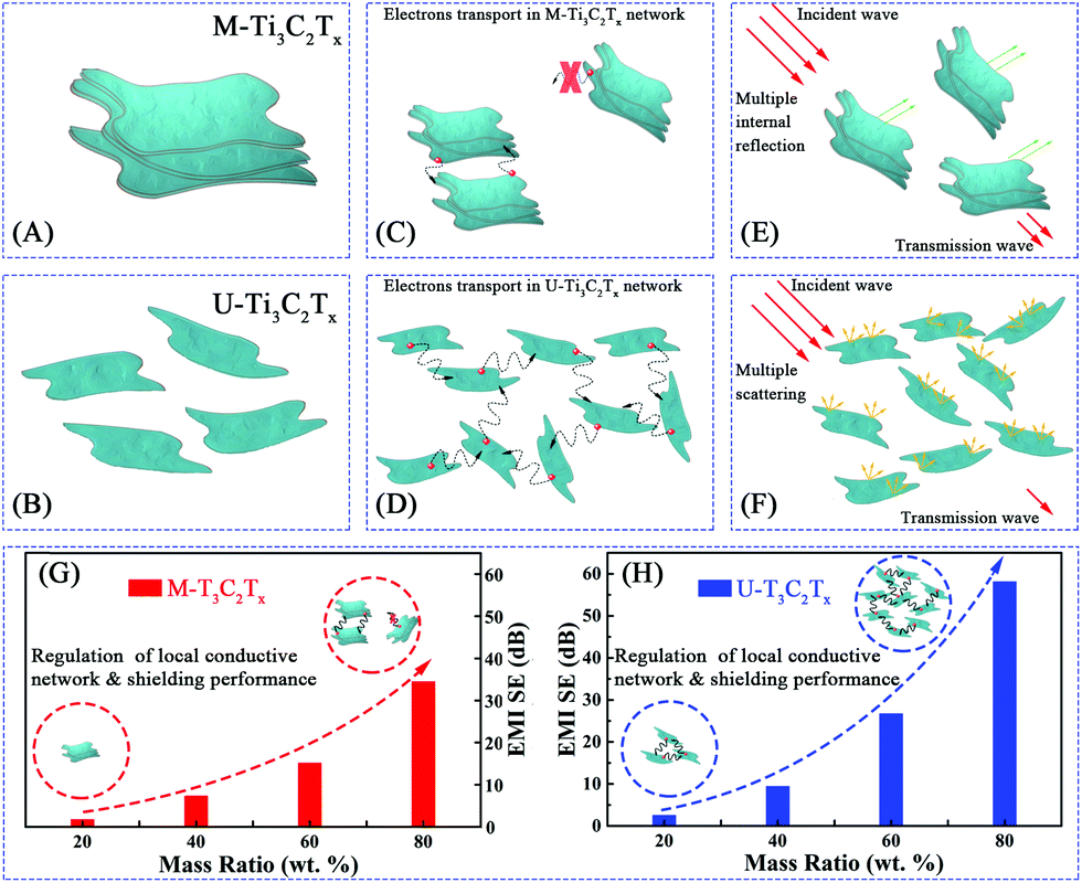 | ||
| Fig. 10 Microstructure of (A) M-Ti3C2Tx and (B) U-Ti3C2Tx. Local conductive network of (C) M-Ti3C2Tx and (D) U-Ti3C2Tx. Microwave propagation model in (E) M-Ti3C2Tx and (F) U-Ti3C2Tx composites. Regulation of local conductive network and shielding performance for (G) M-T3C2Tx and (H) U-Ti3C2Tx. | ||
Conclusions
In summary, U-Ti3C2Tx MXene NS was successfully fabricated by a modified Gogotsi's method. By ALT the layer thicknesses of Ti3C2Tx NS to induce the formation of the local conductive network, high-performance EMI shielding U-Ti3C2Tx NS composites were obtained. The U-Ti3C2Tx NS composites could effectively reduce secondary reflections, demonstrating environmentally friendly performances. We have found that electron transport has an important contribution to EMI shielding performance by comparing the electromagnetic properties of M-Ti3C2Tx and U-Ti3C2Tx MXenes. Furthermore, the defects and terminal atoms can lead to dipoles, in-turn causing polarization, which has a critical contribution to EM attenuation. The EMI attenuation and shielding effectiveness can be effectively tuned by tailoring the local conductive networks. Our findings will provide a new way for designing 2D materials in the future and will help to expand the application of U-Ti3C2Tx MXene NS to other areas such as energy storage, microwave absorption, and metamaterial design.Conflicts of interest
There are no conflicts of interest to declare.Acknowledgements
Financial support from the National Natural Science Foundation of China (No. 11774027, 51132002, 51072024 and 51372282), and Graduate Technological Innovation Project of Beijing Institute of Technology (2018CX20028) are gratefully acknowledged.Notes and references
- C. Liang, Z. Wang, L. Wu, X. Zhang, H. Wang and Z. Wang, ACS Appl. Mater. Interfaces, 2017, 9, 29950–29957 CrossRef CAS.
- H. Wang, L. Xiang, W. Wei, J. An, J. He, C. Gong and Y. Hou, ACS Appl. Mater. Interfaces, 2017, 9, 42102–42110 CrossRef CAS.
- C. Tian, Y. Du, P. Xu, R. Qiang, Y. Wang, D. Ding, J. Xue, J. Ma, H. Zhao and X. Han, ACS Appl. Mater. Interfaces, 2015, 7, 20090–20099 CrossRef CAS.
- D. Estevez, F. X. Qin, L. Quan, Y. Luo, X. F. Zheng, H. Wang and H. X. Peng, Carbon, 2018, 132, 486–494 CrossRef CAS.
- Q. Liu, X. Liu, H. Feng, H. Shui and R. Yu, Chem. Eng. J., 2017, 314, 320–327 CrossRef CAS.
- W. Liu, Q. Shao, G. Ji, X. Liang, Y. Cheng, B. Quan and Y. Du, Chem. Eng. J., 2017, 313, 734–744 CrossRef CAS.
- L. Liu, S. Zhang, F. Yan, C. Li, C. Zhu, X. Zhang and Y. Chen, ACS Appl. Mater. Interfaces, 2018, 10, 14108–14115 CrossRef CAS.
- R. B. Yang, P. M. Reddy, C. J. Chang, P. A. Chen, J. K. Chen and C. C. Chang, Chem. Eng. J., 2016, 285, 497–507 CrossRef CAS.
- X. Liu, X. Nie, R. Yu and H. Feng, Chem. Eng. J., 2018, 334, 153–161 CrossRef CAS.
- J. Lv, X. Liang, G. Ji, B. Quan, W. Liu and Y. Du, ACS Sustainable Chem. Eng., 2018, 6, 7239–7249 CrossRef CAS.
- W. Liu, L. Liu, G. Ji, D. Li, Y. Zhang, J. Ma and Y. Du, ACS Sustainable Chem. Eng., 2017, 5, 7961–7971 CrossRef CAS.
- M. Cao, X. Wang, W. Cao, X. Fang, B. Wen and J. Yuan, Small, 2018, 14, 1800987 CrossRef.
- Y. Cheng, J. Cao, Y. Li, Z. Li, H. Zhao, G. Ji and Y. Du, ACS Sustainable Chem. Eng., 2018, 6, 1427–1435 CrossRef CAS.
- H. Yuan, F. Yan, C. Li, C. Zhu, X. Zhang and Y. Chen, ACS Appl. Mater. Interfaces, 2018, 10, 1399–1407 CrossRef CAS.
- M. Zhang, J. Zhao, Z. Li, S. Ding, Y. Wang, G. Qiu, A. Meng and Q. Li, ACS Sustainable Chem. Eng., 2018, 6, 3596–3603 CrossRef CAS.
- N. Zhou, Q. An, Z. Xiao, S. Zhai and Z. Shi, ACS Sustainable Chem. Eng., 2017, 5, 5394–5407 CrossRef CAS.
- H. Lv, Y. Guo, Z. Yang, T. Guo, H. Wu, G. Liu, L. Wang and R. Wu, ACS Sustainable Chem. Eng., 2018, 6, 1539–1544 CrossRef CAS.
- C. H. Cui, D. X. Yan, H. Pang, L. C. Jia, X. Xu, S. Yang, J. Z. Xu and Z. M. L, Chem. Eng. J., 2017, 323, 29–36 CrossRef CAS.
- L. Wang, Y. Guan, X. Qiu, H. Zhu, S. Pan, M. Yu and Q. Zhang, Chem. Eng. J., 2017, 326, 945–955 CrossRef CAS.
- C. Zhang, B. Wang, J. Xiang, C. Su, C. Mu, F. Wen and Z. Liu, ACS Appl. Mater. Interfaces, 2017, 9, 28868–28875 CrossRef CAS.
- P. Wang, L. Cheng and L. Zhang, Chem. Eng. J., 2018, 338, 248–260 CrossRef CAS.
- J. Kuang, P. Jiang, F. Ran and W. Cao, J. Alloys Compd., 2016, 687, 227–231 CrossRef CAS.
- T. Wu, Y. Zhao, Y. Li, W. Wu and G. Tong, ChemCatChem, 2017, 9, 3486–3496 CrossRef CAS.
- P. Zhao, C. Liang, X. Gong, R. Gao, J. Liu, M. Wang and R. Che, Nanoscale, 2013, 5, 8022–8028 RSC.
- G. Wang, X. Peng, L. Yu, G. Wan, S. Lin and Y. Qin, J. Mater. Chem. A, 2015, 3, 2734–2740 RSC.
- Y. Duan, H. Pang, Y. Zhang, J. Chen and T. Wang, Mater. Charact., 2016, 112, 206–212 CrossRef CAS.
- Q. Li, J. Liu, Y. Zhao, X. Zhao, W. You, X. Li and R. Che, ACS Appl. Mater. Interfaces, 2018, 10, 27540–27547 CrossRef CAS.
- F. Xia, J. Liu, D. Gu, P. Zhao, J. Zhang and R. Che, Nanoscale, 2011, 3, 3860–3867 RSC.
- X. Zhang, G. Ji, W. Liu, X. Zhang, Q. Gao, Y. Li and Y. Du, J. Mater. Chem. C, 2016, 4, 1860–1870 RSC.
- B. Quan, X. Liang, G. Ji, J. Ma, P. Ouyang, H. Gong, G. Xu and Y. Du, ACS Appl. Mater. Interfaces, 2017, 9, 9964–9974 CrossRef CAS.
- W. Liu, L. Liu, Z. Yang, J. Xu, Y. Hou and G. Ji, ACS Appl. Mater. Interfaces, 2018, 10, 8965–8975 CrossRef CAS PubMed.
- Y. Cheng, Z. Li, Y. Li, S. Dai, G. Ji, H. Zhao, J. Cao and Y. Du, Carbon, 2018, 127, 643–652 CrossRef CAS.
- H. Lv, Z. Yang, P. L. Wang, G. Ji, J. Song, L. Zheng, H. Zeng and Z. J. Xu, Adv. Mater., 2018, 30, 1706343 CrossRef.
- J. Ling, W. Zhai, W. Feng, B. Shen, J. Zhang and W. Zheng, ACS Appl. Mater. Interfaces, 2013, 5, 2677–2684 CrossRef CAS.
- B. Wen, M. Cao, M. Lu, W. Cao, H. Shi, J. Liu, X. Wang, H. Jin, X. Fang, W. Wang and J. Yuan, Adv. Mater., 2014, 26, 3484–3489 CrossRef CAS PubMed.
- B. Shen, W. Zhai, M. Tao, J. Ling and W. Zheng, ACS Appl. Mater. Interfaces, 2013, 5, 11383–11391 CrossRef CAS.
- Y. Qing, Q. Wen, F. Luo, W. Zhou and D. Zhu, J. Mater. Chem. C, 2016, 4, 371–375 RSC.
- P. Liu, Y. Huang and X. Sun, ACS Appl. Mater. Interfaces, 2013, 5, 12355–12360 CrossRef CAS.
- X. X. Wang, T. Ma, J. C. Shu and M. S. Cao, Chem. Eng. J., 2018, 332, 321–330 CrossRef CAS.
- G. Wang, Z. Gao, G. Wan, S. Lin, P. Yang and Y. Qin, Nano Res., 2014, 7, 704–716 CrossRef CAS.
- B. Wen, X. X. Wang, W. Q. Cao, H. L. Shi, M. M. Lu, G. Wang, H. B. Jin, W. Z. Wang, J. Yuan and M. S. Cao, Nanoscale, 2014, 6, 5754–5761 RSC.
- M. Naguib, M. Kurtoglu, V. Presser, J. Lu, J. Niu, M. Heon, L. Hultman, Y. Gogotsi and M. W. Barsoum, Adv. Mater., 2011, 23, 4248–4253 CrossRef CAS.
- M. Ghidiu, M. R. Lukatskaya, M. Q. Zhao, Y. Gogotsi and M. W. Barsoum, Nature, 2014, 516, 78–81 CAS.
- M. R. Lukatskaya, O. Mashtalir, C. E. Ren, Y. Dall'Agnese, P. Rozier, P. L. Taberna, M. Naguib, P. Simon, M. W. Barsoum and Y. Gogotsi, Science, 2013, 341, 1502–1505 CrossRef CAS.
- X. Wang, S. Kajiyama, H. Iinuma, E. Hosono, S. Oro, I. Moriguchi and M. Okubo, Nat. Commun., 2015, 6, 6544 CrossRef CAS.
- L. Chen, H. Jiang, H. Jiang, H. Zhang, S. Guo, Y. Hu and C. Li, Adv. Energy Mater., 2017, 7, 1602782 CrossRef.
- Z. Deng, H. Jiang, Y. Hu and C. Li, AIChE J., 2018, 64, 1965–1974 CrossRef CAS.
- C. E. Ren, K. B. Hatzell, M. Alhabeb, Z. Ling, K. A. Mahmoud and Y. Gogotsi, J. Phys. Chem. Lett., 2015, 6, 4026–4031 CrossRef CAS.
- Z. W. Seh, K. D. Fredrickson, B. Anasori, J. Kibsgaard, A. L. Strickler, M. R. Lukatskaya, Y. Gogotsi, T. F. Jaramillo and A. Vojvodic, ACS Energy Lett., 2016, 1, 589–594 CrossRef CAS.
- K. Hantanasirisakul, M. Q. Zhao, P. Urbankowski, J. Halim, B. Anasori, S. Kota, C. E. Ren, M. W. Barsoum and Y. Gogotsi, Adv. Electron. Mater., 2016, 2, 1600050 CrossRef.
- B. Anasori, M. R. Lukatskaya and Y. Gogotsi, Nat. Rev. Mater., 2017, 2, 16098 CrossRef CAS.
- K. Ma, H. Jiang, Y. Hu and C. Li, Adv. Funct. Mater., 2018, 28, 1804306 CrossRef.
- F. Shahzad, M. Alhabeb, C. B. Hatter, B. Anasori, S. M. Hong, C. M. Koo and Y. Gogotsi, Science, 2016, 353, 1137–1140 CrossRef CAS.
- M. Han, X. Yin, H. Wu, Z. Hou, C. Song, X. Li, L. Zhang and L. Cheng, ACS Appl. Mater. Interfaces, 2016, 8, 21011–21019 CrossRef CAS.
- M. Han, X. Yin, X. Li, B. Anasori, L. Zhang, L. Cheng and Y. Gogotsi, ACS Appl. Mater. Interfaces, 2017, 9, 20038–20045 CrossRef CAS.
- X. Li, X. Yin, M. Han, C. Song, H. Xu, Z. Hou, L. Zhang and L. Cheng, J. Mater. Chem. C, 2017, 5, 4068–4074 RSC.
- X. Li, X. Yin, M. Han, C. Song, H. Xu, Z. Hou, L. Zhang and L. Cheng, J. Mater. Chem. C, 2017, 5, 7621–7628 RSC.
- J. Liu, H. B. Zhang, R. Sun, Y. Liu, Z. Liu, A. Zhou and Z. Z. Yu, Adv. Mater., 2017, 29, 1702367 CrossRef.
- G. Xu, X. Wang, S. Gong, S. Wei, J. Liu and Y. Xu, Nanotechnology, 2018, 29, 355201 CrossRef.
- B. Dai, B. Zhao, X. Xie, T. Su, B. Fan, R. Zhang and R. Yang, J. Mater. Chem. C, 2018, 6, 5690–5697 RSC.
- W. T. Cao, F. F. Chen, Y. J. Zhu, Y. G. Zhang, Y. Y. Jiang, M. G. Ma and F. Chen, ACS Nano, 2018, 12, 4583–4593 CrossRef CAS.
- Y. Tong, M. He, Y. Zhou, X. Zhong, L. Fan, T. Huang, Q. Liao and Y. Wang, Appl. Surf. Sci., 2018, 434, 283–293 CrossRef CAS.
- H. Luo, W. Feng, C. Liao, L. Deng, S. Liu, H. Zhang and P. Xiao, J. Appl. Phys., 2018, 123, 104103 CrossRef.
- G. Choi, F. Shahzad, Y. M. Bahk, Y. M. Jhon, H. Park, M. Alhabeb, B. Anasori, D. S. Kim, C. M. Koo, Y. Gogotsi and M. Seo, Adv. Opt. Mater., 2018, 6, 1701076 CrossRef.
- X. Liu, J. Wu, J. He and L. Zhang, Mater. Lett., 2017, 205, 261–263 CrossRef CAS.
- H. Yang, J. Dai, X. Liu, Y. Lin, J. Wang, L. Wang and F. Wang, Mater. Chem. Phys., 2017, 200, 179–186 CrossRef CAS.
- Y. Qian, H. Wei, J. Dong, Y. Du, X. Fang, W. Zheng, Y. Sunc and Z. Jiang, Ceram. Int., 2017, 43, 10757–10762 CrossRef CAS.
- Y. Li, X. Zhou, J. Wang, Q. Deng, M. Li, S. Du, Y. H. Han, J. Lee and Q. Huang, RSC Adv., 2017, 7, 24698–24708 RSC.
- Y. Qing, W. Zhou, F. Luo and D. Zhu, Ceram. Int., 2016, 142, 16412–16416 CrossRef.
- S. Dai, Y. Cheng, B. Quan, X. Liang, W. Liu, Z. Yang, G. Ji and Y. Du, Nanoscale, 2018, 10, 6945–6953 RSC.
- M. S. Cao, Y. Z. Cai, P. He, J. C. Shu, W. Q. Cao and J. Yuan, Chem. Eng. J., 2019, 359, 1265–1302 CrossRef CAS.
- R. Zhao, M. Wang, D. Zhao, H. Li, C. Wang and L. Yin, ACS Energy Lett., 2018, 3, 132–140 CrossRef CAS.
- M. A. Hope, A. C. Forse, K. J. Griffith, M. R. Lukatskaya, M. Ghidiu and Y. Gogotsi, Phys. Chem. Chem. Phys., 2016, 18, 5099–5102 RSC.
- B. Akuzum, K. Maleski, B. Anasori, P. Lelyukh, N. J. Alvarez, E. C. Kumbur and Y. Gogotsi, ACS Nano, 2018, 12, 2685–2694 CrossRef CAS.
- M. Alhabeb, K. Maleski, B. Anasori, P. Lelyukh, L. Clark, S. Sin and Y. Gogotsi, Chem. Mater., 2017, 29, 7633–7644 CrossRef CAS.
- C. J. Zhang, S. Pinilla, N. McEvoy, C. P. Cullen, B. Anasori, E. Long, S. H. Park, A. S. Ascaso, A. Shmeliov, D. Krishnan, C. Morant, X. Liu, G. S. Duesberg, Y. Gogotsi and V. Nicolosi, Chem. Mater., 2017, 29, 4848–4856 CrossRef CAS.
- A. Lipatov, M. Alhabeb, M. R. Lukatskaya, A. Boson, Y. Gogotsi and A. Sinitskii, Adv. Electron. Mater., 2016, 2, 1600255 CrossRef.
- X. Sang, Y. Xie, M. W. Lin, M. Alhabeb, K. L. V. Aken, Y. Gogotsi, P. R. C. Kent, K. Xiao and R. R. Unocic, ACS Nano, 2016, 10, 9193–9200 CrossRef CAS.
- L. H. Karlsson, J. Birch, J. Halim, M. W. Barsoum and P. O. A. Persson, Nano Lett., 2015, 15, 4955–4960 CrossRef CAS.
- C. H. Cui, D. X. Yan, H. Pang, X. Xu, L. C. Jia and Z. M. Li, ACS Sustainable Chem. Eng., 2016, 4, 4137–4145 CrossRef CAS.
- B. Shen, Y. Li, W. Zhai and W. Zheng, ACS Appl. Mater. Interfaces, 2016, 8, 8050–8057 CrossRef CAS.
- X. Y. Fang, X. X. Yu, H. M. Zheng, H. B. Jin, L. Wang and M. S. Cao, Phys. Lett. A, 2015, 379, 2245–2251 CrossRef CAS.
- M. Cao, C. Han, X. Wang, M. Zhang, Y. Zhang, J. Shu, H. Yang, X. Fang and J. Yuan, J. Mater. Chem. C, 2018, 6, 4586–4602 RSC.
Footnote |
| † Electronic supplementary information (ESI) available. See DOI: 10.1039/c8nr10489a |
| This journal is © The Royal Society of Chemistry 2019 |