
 Open Access Article
 This Open Access Article is licensed under a
 Creative Commons Attribution 3.0 Unported Licence
Ligand-free all-inorganic metal halide nanocubes for fast, ultra-sensitive and self-powered ozone sensors†
K.
Brintakis‡
 a,
E.
Gagaoudakis‡
ab,
A.
Kostopoulou
*a,
V.
Faka
abc,
A.
Argyrou
ac,
V.
Binas
abd,
G.
Kiriakidis
ab and
E.
Stratakis
*ab
a,
E.
Gagaoudakis‡
ab,
A.
Kostopoulou
*a,
V.
Faka
abc,
A.
Argyrou
ac,
V.
Binas
abd,
G.
Kiriakidis
ab and
E.
Stratakis
*ab
aInstitute of Electronic Structure & Laser (IESL), Foundation for Research and Technology (FORTH) Hellas, P.O. Box 1385, Heraklion 70013, Crete, Greece. E-mail: akosto@iesl.forth.gr; stratak@iesl.forth.gr
bUniversity of Crete, Department of Physics, 710 03 Heraklion, Crete, Greece
cUniversity of Crete, Department of Materials Science and Technology, 710 03 Heraklion, Crete, Greece
dCrete Center for Quantum Complexity and Nanotechnology, Department of Physics, University of Crete, 71003 Heraklion, Greece
First published on 22nd May 2019
Abstract
Ligand-free all-inorganic lead halide nanocubes have been investigated as ozone sensing materials operating at room temperature. It is found that the nanocubes, crystallined in the orthorhombic CsPbBr3 structure, can operate at room temperature, be self-powered and exhibit high sensitivity and remarkable repeatability. More importantly, they demonstrate higher sensitivity (54% in 187 ppb) and faster response and recovery times compared to hybrid lead mixed halide perovskite (CH3NH3PbI3−xClx) layers, which is the only lead halide perovskite material tested for ozone sensing, to date. Following the exposure to an ozone environment, the stoichiometry and the morphology of the nanocubes remain unaltered. The facile and easy fabrication process together with the high responsivity and stability to the ozone environment makes the bare CsPbBr3 nanocubes a promising material for sensing applications. The sensing properties of the nanoparticulate metal halides presented here provide new exciting opportunities towards engineering reliable and cheap sensing elements for room-temperature operated and self-powered sensors.
A. Introduction
Perovskites are the materials with the formula ABX3, where a cation ‘A’ occupies the corner positions and a cation ‘B’ the center of the unit cell, while an anion ‘X’ is located at the unit cell faces.1 The material family of perovskites includes several oxides, as well as metal halides. The compositional/structural features or the physical properties (optical and electrical) of those materials have been found to change upon an external stimulus such as humidity variations, gas exposure or temperature difference.2,3 Owing to this property, perovskite oxides have been successfully tested as sensing elements to detect analytes including humidity,4,5 gases6–23 and temperature changes.5 More recently, metal halide perovskites, which demonstrate attractive opto-electronic properties for photovoltaic applications,24 have also been tested as sensing materials. In this case, reversible variations of their fluorescence, phosphorescence or chemical resistivity upon applying an external stimulus due to intercalation processes, surface absorption, trap passivation or ion exchange have been reported and used for temperature,25 humidity,26–28 gas29–36 and metal ion37–39 sensing.At the same time, the intense research interest for developing new sensors featuring high sensitivity, high selectivity, fast response and long-term stability leads to test, nanostructured materials as sensing elements. The structuring of the matter at the nanoscale offers a high surface-to-volume ratio, which favours the adsorption of gases on the sensing material due to higher interaction between the analyte and the sensing part.35 Despite the large variety of colloidal synthesis procedures for nanomaterials of high crystallinity quality and finely tuned size, shape, and composition,40–45 only a few examples have been reported for sensing applications by using such materials. Among them, nanostructured metal halide materials have been used for sensing metal ions (copper or mercury),37,39 gases (hydrochloric acid or oxygen)33,34 and humidity.26
According to our knowledge there is no sensor based on metal halide nanostructures for ozone gas sensing. The ozone is detected both in the Earth's upper atmosphere and at the ground level. Ground level ozone which is called “bad ozone” is produced from the reaction between nitrogen oxides and hydrocarbons, when pollutants are emitted by cars, chemical solvents and industrial releases.46 Ozone is highly toxic when its concentration in the air exceeds 1 ppm. Breathing ozone can trigger a variety of health problems including chest pain, coughing, throat irritation, and congestion.47 It can worsen bronchitis, emphysema, and asthma and can also reduce lung function and inflame the linings of the lungs. Repeated exposure may permanently scar lung tissue. Ozone at concentrations higher than 50 ppm presents risks to life, and an ozone concentration of 1000 ppm or more, causes death in a short time.48 Thus, ozone sensors are crucial for our modern life well-being, providing us information for health protection.
Ozone sensors can be classified according to the property/feature used for sensing as optical,49 optochemical,50 electrochemical51 and conductometric52 and the sensing materials in these cases are metal oxides such as In2O3, SnO2, WO3, TiO2, CuAlO2, and SmFeO3 in the film form.53 The responsiveness and the sensitivity of ozone sensors in these cases can be affected by metal oxide synthesis/film deposition through factors, such as film thickness, film porosity and grain size.53 These ozone sensors operate at temperatures well above room temperature, their sensitivity is limited to a few hundreds of ppb and they are not self-powered devices, as they require to be switched on before their operation by an external stimuli like UltraViolet (UV) irradiation or heating. In this context, there is an increasing demand for self-powered and ultra-sensitive down to ppb ozone sensing systems.
Recently, an organic–inorganic metal halide film fabricated by a spin coating procedure has been used as a self-powered, ultrasensitive and room-temperature operating ozone sensing material.30 This material can detect ozone concentrations down to a few ppb with a response time of 200 seconds; at the same time, no external stimulus is required to initiate the sensing process. However, the complex and time-consuming fabrication (spin coating and subsequent annealing in an inert atmosphere), together with the short sensor lifetime, due to film degradation under ambient conditions and the reaction with ozone, challenges the scientific community to discover more stable metal halides to be used for this application.
The present work is the first to demonstrate the application, of all-inorganic lead halide nanocrystals as ozone sensing materials with superior operational stability. In particular, well-crystalline and stable under ambient conditions CsPbBr3 nanocubes have been directly grown onto a substrate via a solution-based precipitation method, in a few seconds. It was found that the high active surface area of the nanocubes, together with the enhanced interaction between the ozone analyte and the sensing part, touching directly the electrical contacts, gives rise to high sensitivity and responsiveness with remarkable stability. Indeed, it is shown that the response time is two times lower, compared to that measured for organic–inorganic metal halide films.30 At the same time and contrary to organic–inorganic layers, the response effect is completely reversible. It is concluded that the proposed system, which combines a simple and quick fabrication process with high sensitivity and long-term stability under ambient conditions, is promising for ozone sensing applications.
B. Results and discussion
Fabrication of the ozone sensor
All-inorganic lead halide perovskite nanocubes with sizes ranging from 500 nm to 1 μm have been fabricated directly on a pre-patterned electrode substrate through a simple and fast re-precipitation method at room temperature. Particularly, a small volume of an already prepared precursor solution is deposited on the substrate and then an equal amount of toluene is spread over the whole substrate area (Fig. 1a). Following this process, ligand-free nanocubes, well-defined in shape, have been directly grown onto the substrate (Fig. 1b and c). Similarly, re-precipitation solution-based methods have been used to synthesize different morphologies of metal halide nanocrystals ranging from spheres,54–56 cubes43 and platelets57–59 to more anisotropic morphologies such as nanowires45,58 and nanorods.58,60 Moreover, ligand-free nanocubes grown on substrates by spin coating of the precursor solution, followed by heat treatment,61 have been used as efficient materials for nanolasers.62 X-ray diffraction analysis revealed the high-crystallinity of nanocubes, which is compatible with the orthorhombic structure of CsPbBr3 (ICSD, #97851). At the same time the X-ray diffraction spectra show no indication of a secondary phase. The stoichiometry is also confirmed by EDS analysis (Fig. S1a†) and the calculated energy gap (2.27 eV,) is very close to the reported band gap of the direct single crystal semiconductor CsPbBr3.63 | ||
| Fig. 1 Schematic representation of the ozone sensor fabrication based on CsPbBr3 nanocubes (a), SEM images (b and c) and X-ray diffraction pattern ((d) black curve) of the nanocubes prior to ozone treatment. A reference pattern of the orthorhombic (ICSD, #97851) crystal structure of CsPbBr3 is provided for comparison ((d) red curve). | ||
Sensing properties of the metal halide nanocubes
The nanocube-based sensor is placed into a homemade gas-testing chamber, while the ozone flow is digitally controlled by using a dual cell photometer. The most important parameters to characterize the performance of a sensor are the sensitivity, the response and recovery times, as well as the sensing reversibility. The initial current is measured to be approximately 2 μA (Fig. 2a). This high initial current value is due to the direct contact between the nanoparticulate sensing material and the platinum contacts, as well as the absence of organic ligands around the particles, which could behave as an insulating medium. CsPbBr3 perovskites absorb in the range of 400–500 nm depending on their shape and size, which lies in the visible range, thus explaining the initial current, when the sensor is exposed to ambient light.31,42 This current is two times higher than that of the hybrid organic–inorganic perovskite film (CH3NH3PbI3−xClx) deposited on the same electrode substrate and tested for a similar ozone sensing application.30 It has to be noted that no additional external stimulus is required for the sensor to be switched on to the initial state prior to ozone exposure. This is important in the case of using the sensor in a portable device. The sensing process is initiated by introduction a well-defined ozone flow of 500 sccm (standard cm3 min−1) into the chamber, controlled by using a flowmeter, giving rise to an electrical current increase. The sensor recovered to its original state upon introducing synthetic air in the chamber for 20 min with a similar flow. During the exposure and the recovery processes, the pressure in the chamber was kept constant and equal to 400 mbar. All the experiments were performed at room temperature. Fig. 2a presents the electrical response of the sensor, showing the immediate current increase upon exposure to ozone gas and the respective recovery of the response, within a few seconds after the ozone gas replacement with synthetic air. The same behaviour is observed for all tested ozone concentrations ranging from 2650 down to 4 ppb. The time in which the sensor can detect ozone is less than 1 min, indicating its fast response (Fig. 2b). Fig. 2c shows the detailed evolution of the maximum and the minimum current values, Imax and Imin, as a function of the respective ozone concentrations tested. It can be observed that Imax increases upon increasing the ozone concentration, which is not the case for the minimum current value, which is always close to the starting value. The corresponding material sensitivity, calculated from the ratio [(Imax − Imin)/Imin] × 100% (Fig. 2c, red stars) is increased from 1.3% for 4 ppb to almost 428% for 2650 ppb ozone concentration. The 187 ppb corresponds to the ozone level that the sensor can measure with certainty, with 54% sensitivity. The position of our sensing element among the other reported semiconducting materials for ozone sensing30,64–73 is illustrated in Fig. 3. It can be observed that the nanocubes we report here exhibit the highest sensitivity amongst the other competitors under room temperature working conditions and detect the lowest ozone concentrations.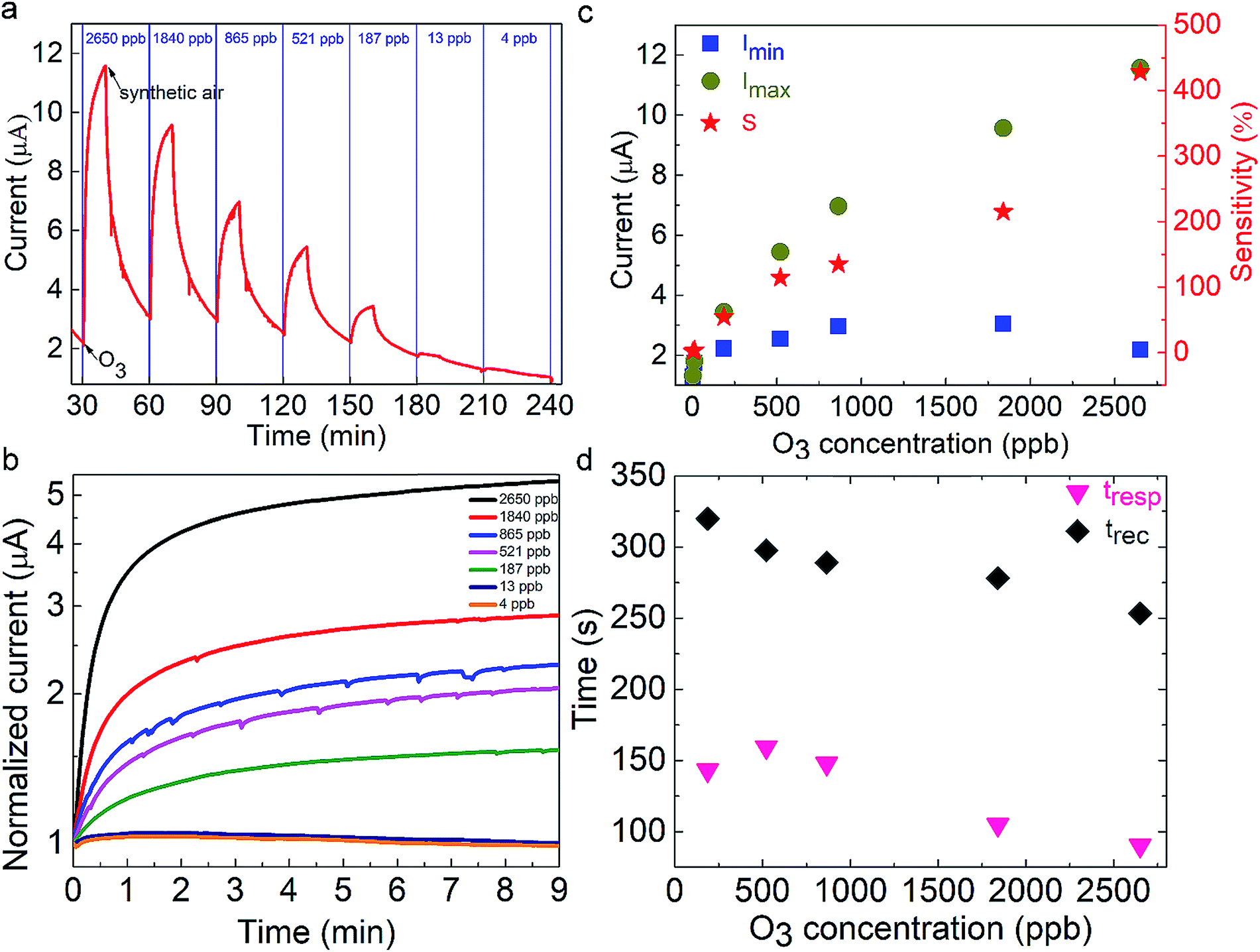 | ||
| Fig. 2 Electrical response of the all-inorganic perovskite nanocubes as sensing materials upon applying various ozone concentrations from 2650 down to 4 ppb as a function of the ozone exposure time (a and b). Sensitivity (S) and response (tres) and recovery time (trec) as a function of gas concentration of the nanocube-based sensor (c and d). | ||
 | ||
| Fig. 3 Sensitivity vs. O3 concentration and working temperature for the sensing elements found in the literature. The blue frame indicates the room temperature regime. | ||
Two important parameters that determine the sensor quality are the response (tres) and the recovery (trec) times. The former is defined as the time taken by the electrical current to reach 90% of its maximum value under an ozone flow, while the latter is the time taken by the current to become 10% of its maximum value, upon ozone removal. Fig. 2d presents the evolution of tres and trec with the ozone concentration. Notably, tres values lie between 100 s and 150 s while trec is between 250 s and 320 s. These values are almost two times higher than those measured for hybrid metal-halide thin films. Furthermore, the response time is almost unchanged for concentrations below 865 ppb and decreases at higher ones. In contrast, the recovery time decreases upon increasing the concentration. These values are close to those reported in the literature for O3 sensing materials (Fig. S2 and Table S1†). In particular, the response time of the nanocubes reported here is faster compared to that of hybrid organic–inorganic metal halides used as sensing elements and in the same order as that of oxides. Significantly faster response times were observed for diphasic sensing elements (NiAl-LDH,65 TiO2–In2O3,67 ZnO–SnO2 (ref. 68) and Au@TiO2 (ref. 64)). However, these materials are synthesized with more complex and time-consuming fabrication processes compared to the solution-processed direct growth proposed in this work.
Short-term stability of the sensor
The analysis of the sensing properties in successive ozone/synthetic air switching cycles revealed a remarkable repeatability and stability of the fabricated sensors. In particular, following ozone exposure, the induced current rapidly increases by six times and readily recovers to its initial value upon ozone removal (Fig. 4a). However, it is noted that after a number of successive cycles the current does not fully reverse to its initial value, possibly due to residual adsorbed ozone molecules. O2 passivation of surface hole-traps has been observed in nanocrystals of a similar phase.74,75 As shown in Fig. 4b, S3b and c†, following a series of four sensing cycles, the nanocubes retain their morphological and stoichiometric features. This can be attributed to the good crystallinity of the nanocubes (Fig. 5a black curve) on the one hand and the fact that no coalescence effects have been observed after ozone treatment, which could degrade the performance of the sensing layer (Fig. 5a red curve).76 | ||
| Fig. 4 Time dependence of the ozone response upon four successive sensing scans (a) and SEM image of the all-inorganic perovskite nanocubes at the end of the sensing process (b). | ||
 | ||
| Fig. 5 (a) Corresponding XRD patterns of the sensing material before (lower) and three months after the ozone exposure (upper) (images are presented in Fig S3†). (b) Electrical response of an all-inorganic perovskite nanocube sensor as a function of the ozone exposure time at various concentrations in the as-prepared state (blue curve) and that obtained upon the sensor storage for three months under ambient conditions (red curve). | ||
Long-term stability
The long-term degradation of the sensing performance has been additionally investigated (Fig. 5b), via recording the electrical response of sensor stored for three months under ambient conditions. It is observed that, although the absolute current values are found to be a bit higher, the response and trend are similar to those in the 1st sensing cycle, for all ozone concentrations tested (Fig. 5b). In order to elaborate possible phase changes upon the prolonged exposure to ambient conditions, the XRD pattern of the stored sample is compared to that of the as-prepared one, in Fig. 5a. This comparison indicates that there are no phase alterations or impurity formation. SEM imaging also reveals that the crystals preserve their pristine shape and morphology (Fig. S3†).Proposed sensing mechanism
The absence of any phase transformation and impurity formation, upon exposure to an ozone atmosphere, indicates that the sensing mechanism is different to those reported to date, in which they attribute the sensing effect to a chemical reaction of the perovskite crystals with the gas molecules. For example, molecular dynamics simulations demonstrated that when a perovskite is under a NH3 gas environment, the NH3 molecule has a tendency to diffuse from the outermost surface layer into the perovskite underlayer leading to distortion of the perovskite lattice.77 Moreover, several experimental studies show either an enhancement of the XRD peaks' intensity upon gas exposure, attributed to crystallinity improvement,78 or a completely different XRD pattern indicating the formation of a completely new structure.36,79,80 In our case such a behaviour is not observed. We can postulate though that our results could be interpreted according to Wolkenstein's model81 described below. In particular, when the sensor is exposed to air, adsorbed neutral oxygen molecules (O2)ads onto the perovskite surface become partially ionized into O2−, O− and O2− ions by attracting electrons from the semiconductor valence band. As a consequence, an accumulation layer of holes with lower resistance, covering the whole surface of the nanocubes, is formed due to the reduction in the number of electrons (Fig. 6a). Thus, before the exposure to ozone gas, a core–shell cubic configuration with a resistive core and a conductive hole shell is shaped.82 Then, the electrical current is increased due to the adsorption of ozone molecules (electron acceptor), which increases the number of holes in the CsPbBr3 perovskite shell lattice. The increasing electron trapping from the valence band of the sensing perovskite element leads to the increase of the current, which is a p-type electrical behaviour (Fig. 6b).83 A similar sensing mechanism has been proposed in the case of a photoexcited porous network of the same perovskite phase upon O2 exposure.31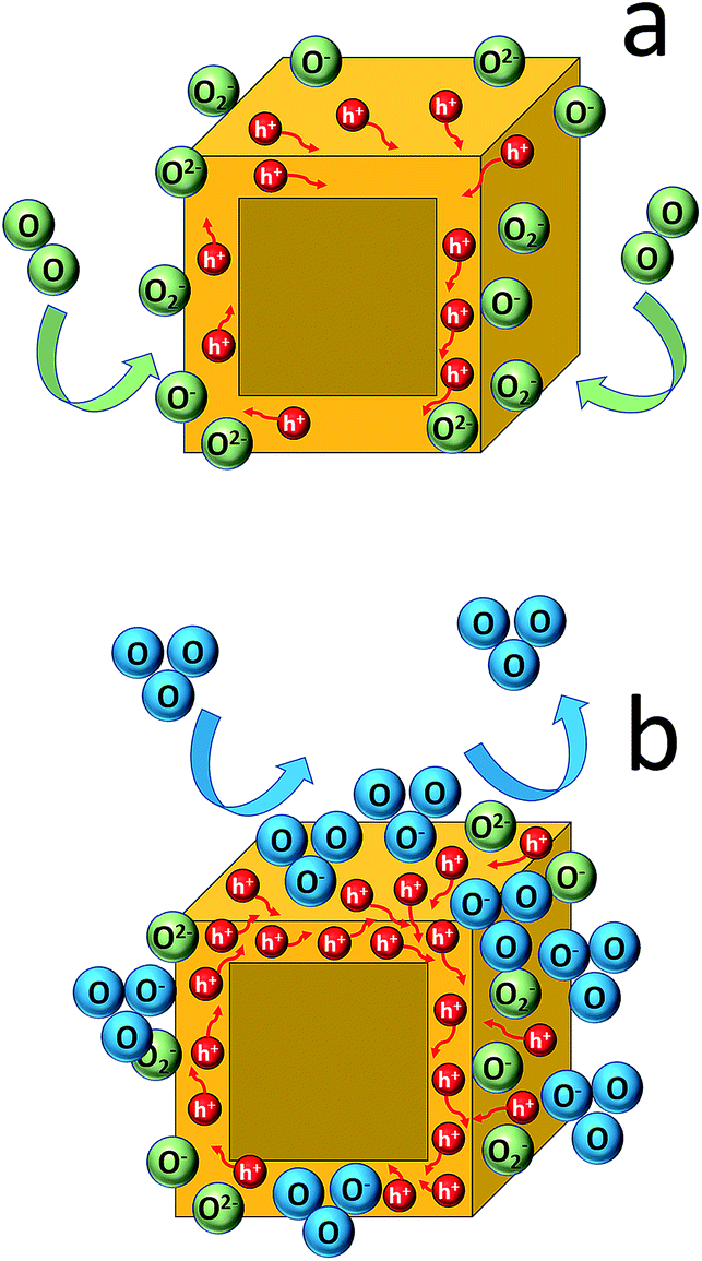 | ||
| Fig. 6 Schematic diagram of the gas sensing mechanism under ambient conditions (a) and after ozone exposure (b). | ||
C. Experimental
Materials and methods
D. Conclusions
It has been demonstrated that the direct growth of ligand-free, all-inorganic metal halide nanocubes from solution is a convenient preparation method for highly sensitive and durable ozone sensors. The main advantage of this technique is its simplicity as well as the cost-effective fabrication. The sensor is able to work at room temperature, without the need for external stimuli (i.e. self-powered), such as UV irradiation or heating and it is fully reversible following the ozone withdrawal. Its sensitivity (54% at 187 ppb ozone concentration) is the highest among those reported in the literature. Furthermore, its sensitivity and durability are by far better than those of the hybrid organic–inorganic metal halide sensing film, which is the only lead halide perovskite material tested for ozone sensing to date, which it lacks stability as it degrades upon exposure to humidity and oxygen. Besides this, the response time is comparable to that of oxides; however, the simplicity of the synthesis process, as well as the use of solely commercially available reactants and solvents, brings about a breakthrough step in gas sensors' development.This is the first report on the use of all-inorganic metal halide perovskite nanostructures as ozone sensing elements and it will give the pace for further studies of new perovskite materials, such as lead-free compounds, for gas sensing applications.
Conflicts of interest
There are no conflicts to declare.Acknowledgements
This project has received funding from the Hellenic Foundation for Research and Innovation (HFRI) and the General Secretariat for Re-search and Technology (GSRT), under grand agreement No 1179. We are grateful to Dr Alexandros Lappas for the access to the Functional Nanocrystals & Quantum Magnetism Laboratory at the Institute of Electronic Structure and Laser, Foundation for Research & Technology – Hellas (FORTH) to perform the synthesis of the perovskites.Notes and references
- Q. A. Akkerman, G. Rainò, M. V. Kovalenko and L. Manna, Nat. Mater., 2018, 17, 394–405 CrossRef CAS PubMed.
- Z. Zhu, Q. Sun, Z. Zhang, J. Dai, G. Xing, S. Li, X. Huang and W. Huang, J. Mater. Chem. C, 2018, 6, 10121–10137 RSC.
- J. W. Fergus, Sens. Actuators, B, 2007, 123, 1169–1179 CrossRef CAS.
- M. Viviani, M. T. Buscaglia, V. Buscaglia, M. Leoni and P. Nanni, J. Eur. Ceram. Soc., 2001, 21, 1981–1984 CrossRef CAS.
- C. de la Torre-Gamarra, M. Woszczak, B. Levenfeld, A. Varez, E. García-González, E. Urones-Garrote and V. Di Noto, J. Mater. Chem. A, 2018, 6, 5430–5442 RSC.
- Y. M. Zhang, Y. T. Lin, J. L. Chen, J. Zhang, Z. Q. Zhu and Q. J. Liu, Sens. Actuators, B, 2014, 190, 171–176 CrossRef CAS.
- Y. Chen, H. Qin, X. Wang, L. Li and J. Hu, Sens. Actuators, B, 2016, 235, 56–66 CrossRef CAS.
- M. Mori, Y. Itagaki and Y. Sadaoka, Sens. Actuators, B, 2012, 163, 44–50 CrossRef CAS.
- L. Gómez, V. Galeano, R. Parra, C. R. Michel, C. Paucar and O. Morán, Sens. Actuators, B, 2015, 221, 1455–1460 CrossRef.
- E. Delgado and C. R. Michel, Mater. Lett., 2006, 60, 1613–1616 CrossRef CAS.
- X. Wang, H. Qin, L. Sun and J. Hu, Sens. Actuators, B, 2013, 188, 965–971 CrossRef CAS.
- E. Cao, Z. Chu, H. Wang, W. Hao, L. Sun and Y. Zhang, Ceram. Int., 2018, 44, 7180–7185 CrossRef CAS.
- E. Cao, Y. Yang, T. Cui, Y. Zhang, W. Hao, L. Sun, H. Peng and X. Deng, Appl. Surf. Sci., 2017, 393, 134–143 CrossRef CAS.
- S. Misra, Mater. Chem. Phys., 2017, 190, 1–7 CrossRef CAS.
- T. Addabbo, F. Bertocci, A. Fort, M. Gregorkiewitz, M. Mugnaini, R. Spinicci and V. Vignoli, Sens. Actuators, B, 2017, 244, 1054–1070 CrossRef CAS.
- B. Wang, Q. Yu, S. Zhang, T. Wang, P. Sun, X. Chuai and G. Lu, Sens. Actuators, B, 2018, 258, 1215–1222 CrossRef CAS.
- L. Gildo-Ortiz, H. Guillén-Bonilla, V. M. Rodríguez-Betancourtt, O. Blanco-Alonso, A. Guillén-Bonilla, J. Santoyo-Salazar, I. C. Romero-Ibarra and J. Reyes-Gómez, Ceram. Int., 2018, 44, 15402–15410 CrossRef CAS.
- P. Dhivya, A. K. Prasad and M. Sridharan, Sens. Actuators, B, 2016, 222, 987–993 CrossRef CAS.
- W. Haron, A. Wisitsoraat and S. Wongnawa, Ceram. Int., 2017, 43, 5032–5040 CrossRef CAS.
- V. R. Mastelaro, S. C. Zílio, L. F. da Silva, P. I. Pelissari, M. I. B. Bernardi, J. Guerin and K. Aguir, Sens. Actuators, B, 2013, 181, 919–924 CrossRef CAS.
- L. Ma, S. Y. Ma, Z. Qiang, X. L. Xu, Q. Chen, H. M. Yang, H. Chen, Q. Ge, Q. Z. Zeng and B. Q. Wang, Mater. Lett., 2017, 200, 47–50 CrossRef CAS.
- K. Wetchakun, T. Samerjai, N. Tamaekong, C. Liewhiran, C. Siriwong, V. Kruefu, A. Wisitsoraat, A. Tuantranont and S. Phanichphant, Sens. Actuators, B, 2011, 160, 580–591 CrossRef CAS.
- A. Benali, S. Azizi, M. Bejar, E. Dhahri and M. F. P. Graça, Ceram. Int., 2014, 40, 14367–14373 CrossRef CAS.
- A. Kostopoulou, E. Kymakis and E. Stratakis, J. Mater. Chem. A, 2018, 6, 9765–9798 RSC.
- Y. Niu, F. Zhang, Z. Bai, Y. Dong, J. Yang, R. Liu, B. Zou, J. Li and H. Zhong, Adv. Opt. Mater., 2015, 3, 112–119 CrossRef CAS.
- K. Ren, L. Huang, S. Yue, S. Lu, K. Liu, M. Azam, Z. Wang, Z. Wei, S. Qu and Z. Wang, J. Mater. Chem. C, 2017, 5, 2504–2508 RSC.
- W. Xu, F. Li, Z. Cai, Y. Wang, F. Luo and X. Chen, J. Mater. Chem. C, 2016, 4, 9651–9655 RSC.
- L. Hu, G. Shao, T. Jiang, D. Li, X. Lv, H. Wang, X. Liu, H. Song, J. Tang and H. Liu, ACS Appl. Mater. Interfaces, 2015, 7, 25113–25120 CrossRef CAS PubMed.
- Y. Zhuang, W. Yuan, L. Qian, S. Chen and G. Shi, Phys. Chem. Chem. Phys., 2017, 19, 12876–12881 RSC.
- G. Kakavelakis, E. Gagaoudakis, K. Petridis, V. Petromichelaki, V. Binas, G. Kiriakidis and E. Kymakis, ACS Sens., 2018, 3, 135–142 CrossRef CAS PubMed.
- H. Chen, M. Zhang, R. Bo, C. Barugkin, J. Zheng, Q. Ma, S. Huang, A. W. Y. Ho-Baillie, K. R. Catchpole and A. Tricoli, Small, 2018, 14, 1702571 CrossRef PubMed.
- M. Sygletou, M.-E. Kyriazi, A. G. Kanaras and E. Stratakis, Chem. Sci., 2018, 9, 8121–8126 RSC.
- F. Lin, F. Li, Z. Lai, Z. Cai, Y. Wang, O. S. Wolfbeis and X. Chen, ACS Appl. Mater. Interfaces, 2018, 10, 23335–23343 CrossRef CAS PubMed.
- X. Chen, H. Hu, Z. Xia, W. Gao, W. Gou, Y. Qu and Y. Ma, J. Mater. Chem. C, 2017, 5, 309–313 RSC.
- M.-A. Stoeckel, M. Gobbi, S. Bonacchi, F. Liscio, L. Ferlauto, E. Orgiu and P. Samorì, Adv. Mater., 2017, 29, 1702469 CrossRef PubMed.
- C. Bao, J. Yang, W. Zhu, X. Zhou, H. Gao, F. Li, G. Fu, T. Yu and Z. Zou, Chem. Commun., 2015, 51, 15426–15429 RSC.
- L.-Q. Lu, T. Tan, X.-K. Tian, Y. Li and P. Deng, Anal. Chim. Acta, 2017, 986, 109–114 CrossRef CAS PubMed.
- Y. Liu, X. Tang, T. Zhu, M. Deng, I. P. Ikechukwu, W. Huang, G. Yin, Y. Bai, D. Qu, X. Huang and F. Qiu, J. Mater. Chem. C, 2018, 6, 4793–4799 RSC.
- X. Sheng, Y. Liu, Y. Wang, Y. Li, X. Wang, X. Wang, Z. Dai, J. Bao and X. Xu, Adv. Mater., 2017, 29, 1700150 CrossRef PubMed.
- L. Protesescu, S. Yakunin, M. I. Bodnarchuk, F. Krieg, R. Caputo, C. H. Hendon, R. X. Yang, A. Walsh and M. V. Kovalenko, Nano Lett., 2015, 15, 3692–3696 CrossRef CAS.
- A. Pan, B. He, X. Fan, Z. Liu, J. J. Urban, A. P. Alivisatos, L. He and Y. Liu, ACS Nano, 2016, 10, 7943–7954 CrossRef CAS PubMed.
- J. Shamsi, Z. Dang, P. Bianchini, C. Canale, F. Di Stasio, R. Brescia, M. Prato and L. Manna, J. Am. Chem. Soc., 2016, 138, 7240–7243 CrossRef CAS PubMed.
- X. Li, Y. Wu, S. Zhang, B. Cai, Y. Gu, J. Song and H. Zeng, Adv. Funct. Mater., 2016, 26, 2435–2445 CrossRef CAS.
- S. Sun, D. Yuan, Y. Xu, A. Wang and Z. Deng, ACS Nano, 2016, 10, 3648–3657 CrossRef CAS PubMed.
- A. Kostopoulou, M. Sygletou, K. Brintakis, A. Lappas and E. Stratakis, Nanoscale, 2017, 9, 18202–18207 RSC.
- D. Nuvolone, D. Petri and F. Voller, Environ. Sci. Pollut. Res., 2018, 25, 8074–8088 CrossRef CAS PubMed.
- N. P. Cheremisinoff, Pollution Control Handbook for Oil and Gas Engineering, John Wiley & Sons, 2016 Search PubMed.
- M. Ando, V. Biju and Y. Shigeri, Anal. Sci., 2018, 34, 263–271 CrossRef CAS PubMed.
- D. Lee, J. Jung, D. Bilby, M. S. Kwon, J. Yun and J. Kim, A Novel Optical Ozone Sensor Based on Purely Organic Phosphor, https://pubs.acs.org/doi/abs/10.1021/am5087165, accessed March 28, 2019 Search PubMed.
- G. Korotcenkov, V. Brinzari and B. K. Cho, In2O3- and SnO2-Based Thin Film Ozone Sensors, https://www.hindawi.com/journals/js/2016/3816094/, accessed March 28, 2019 Search PubMed.
- X. Pang, M. D. Shaw, A. C. Lewis, L. J. Carpenter and T. Batchellier, Sens. Actuators, B, 2017, 240, 829–837 CrossRef CAS.
- G. Korotcenkov and B. K. Cho, Sens. Actuators, B, 2012, 161, 28–44 CrossRef CAS.
- G. Korotcenkov, V. Brinzari and B. K. Cho, Crit. Rev. Solid State Mater. Sci., 2018, 43, 83–132 CrossRef CAS.
- L. C. Schmidt, A. Pertegás, S. González-Carrero, O. Malinkiewicz, S. Agouram, G. Mínguez Espallargas, H. J. Bolink, R. E. Galian and J. Pérez-Prieto, J. Am. Chem. Soc., 2014, 136, 850–853 CrossRef CAS PubMed.
- F. Zhang, H. Zhong, C. Chen, X. Wu, X. Hu, H. Huang, J. Han, B. Zou and Y. Dong, ACS Nano, 2015, 9, 4533–4542 CrossRef CAS PubMed.
- Y. Zhang, M. I. Saidaminov, I. Dursun, H. Yang, B. Murali, E. Alarousu, E. Yengel, B. A. Alshankiti, O. M. Bakr and O. F. Mohammed, J. Phys. Chem. Lett., 2017, 8, 961–965 CrossRef CAS PubMed.
- J. A. Sichert, Y. Tong, N. Mutz, M. Vollmer, S. Fischer, K. Z. Milowska, R. García Cortadella, B. Nickel, C. Cardenas-Daw, J. K. Stolarczyk, A. S. Urban and J. Feldmann, Nano Lett., 2015, 15, 6521–6527 CrossRef CAS PubMed.
- F. Zhu, L. Men, Y. Guo, Q. Zhu, U. Bhattacharjee, P. M. Goodwin, J. W. Petrich, E. A. Smith and J. Vela, ACS Nano, 2015, 9, 2948–2959 CrossRef CAS PubMed.
- K.-H. Wang, L. Wu, L. Li, H.-B. Yao, H.-S. Qian and S.-H. Yu, Angew. Chem., Int. Ed., 2016, 55, 8328–8332 CrossRef CAS PubMed.
- S. Aharon and L. Etgar, Nano Lett., 2016, 16, 3230–3235 CrossRef CAS PubMed.
- Z. Hu, Z. Liu, Y. Bian, D. Liu, X. Tang, W. Hu, Z. Zang, M. Zhou, L. Sun, J. Tang, Y. Li, J. Du and Y. Leng, Adv. Opt. Mater., 2017, 5, 1700419 CrossRef.
- Z. Liu, J. Yang, J. Du, Z. Hu, T. Shi, Z. Zhang, Y. Liu, X. Tang, Y. Leng and R. Li, ACS Nano, 2018, 12, 5923–5931 CrossRef CAS PubMed.
- C. C. Stoumpos, C. D. Malliakas, J. A. Peters, Z. Liu, M. Sebastian, J. Im, T. C. Chasapis, A. C. Wibowo, D. Y. Chung, A. J. Freeman, B. W. Wessels and M. G. Kanatzidis, Cryst. Growth Des., 2013, 13, 2722–2727 CrossRef CAS.
- Z. Zhu, J.-L. Chang and R.-J. Wu, Sens. Actuators, B, 2015, 214, 56–62 CrossRef CAS.
- G. Kang, Z. Zhu, B.-H. Tang, C.-H. Wu and R.-J. Wu, Sens. Actuators, B, 2017, 241, 1203–1209 CrossRef CAS.
- S. Gavalas, E. Gagaoudakis, D. Katerinopoulou, V. Petromichelaki, S. Wight, G. Wotring, E. Aperathitis, G. Kiriakidis and V. Binas, Mater. Sci. Semicond. Process., 2019, 89, 116–120 CrossRef CAS.
- C.-H. Wu, T.-L. Chou and R.-J. Wu, Sens. Actuators, B, 2018, 255, 117–124 CrossRef CAS.
- L. F. da Silva, J.-C. M'Peko, A. C. Catto, S. Bernardini, V. R. Mastelaro, K. Aguir, C. Ribeiro and E. Longo, Sens. Actuators, B, 2017, 240, 573–579 CrossRef CAS.
- Z. Wang, A. Sackmann, S. Gao, U. Weimar, G. Lu, S. Liu, T. Zhang and N. Barsan, Sens. Actuators, B, 2019, 285, 590–600 CrossRef CAS.
- D. Ziegler, E. Bekyarova, A. Marchisio, J.-M. Tulliani and K. Naishadham, in 2018 IEEE SENSORS, IEEE, New Delhi, 2018, pp. 1–4 Search PubMed.
- N. Joshi, L. F. da Silva, H. S. Jadhav, F. M. Shimizu, P. H. Suman, J.-C. M'Peko, M. O. Orlandi, J. G. Seo, V. R. Mastelaro and O. N. Oliveira, Sens. Actuators, B, 2018, 257, 906–915 CrossRef CAS.
- Y. J. Onofre, A. C. Catto, S. Bernardini, T. Fiorido, K. Aguir, E. Longo, V. R. Mastelaro, L. F. da Silva and M. P. F. de Godoy, Appl. Surf. Sci., 2019, 478, 347–354 CrossRef CAS.
- Y.-T. Tsai, S.-J. Chang, I.-T. Tang, Y.-J. Hsiao and L.-W. Ji, IEEE Sens. J., 2018, 18, 5559–5565 CAS.
- M. Lorenzon, L. Sortino, Q. Akkerman, S. Accornero, J. Pedrini, M. Prato, V. Pinchetti, F. Meinardi, L. Manna and S. Brovelli, Nano Lett., 2017, 17, 3844–3853 CrossRef CAS PubMed.
- C. Rodà, A. L. Abdelhady, J. Shamsi, M. Lorenzon, V. Pinchetti, M. Gandini, F. Meinardi, L. Manna and S. Brovelli, Nanoscale, 2019, 11, 7613–7623 RSC.
- S. Nicoletti, S. Zampolli, I. Elmi, L. Dori and M. Severi, IEEE Sens. J., 2003, 3, 454–459 CrossRef CAS.
- L. Zhang, F. Yu, Q. Li, J. Su, J. Li and M. Li, J. Phys. D: Appl. Phys., 2018, 51, 315302 CrossRef.
- Z. Zhou, Z. Wang, Y. Zhou, S. Pang, D. Wang, H. Xu, Z. Liu, N. P. Padture and G. Cui, Angew. Chem., Int. Ed., 2015, 54, 9705–9709 CrossRef CAS PubMed.
- S. Ruan, J. Lu, N. Pai, H. Ebendorff-Heidepriem, Y.-B. Cheng, Y. Ruan and C. R. McNeill, J. Mater. Chem. C, 2018, 6, 6988–6995 RSC.
- Y. Zhao and K. Zhu, Chem. Commun., 2014, 50, 1605–1607 RSC.
- F. F. Wolkenshteĭn, Electronic Processes on Semiconductor Surfaces during Chemisorption, Consultants Bureau, New York, 1991 Search PubMed.
- G. Dong, H. Fan, H. Tian, J. Fang and Q. Li, RSC Adv., 2015, 5, 29618–29623 RSC.
- S. Thirumalairajan and V. R. Mastelaro, Sens. Actuators, B, 2016, 223, 138–148 CrossRef CAS.
Footnotes |
| † Electronic supplementary information (ESI) available: EDS spectra of CsPbBr3 nanocubes, before and after ozone exposure and after 3 months. Diagram of response and recovery times of various sensing elements. Table of various sensing elements with their phase, morphology, preparation method, working temperature, sensitivity, operating O3 concentration, response and recovery times. SEM images of CsPbBr3 nanocubes as prepared, after ozone exposure and after 3 months stored under ambient conditions and exposed to ozone again. See DOI: 10.1039/c9na00219g |
| ‡ K. Brintakis and E. Gagaoudakis contributed equally to this work. |
| This journal is © The Royal Society of Chemistry 2019 |