
Coherent control of thermal phonon transport in van der Waals superlattices†
Ruiqiang
Guo
 a,
Young-Dahl
Jho
b and
Austin J.
Minnich
*a
a,
Young-Dahl
Jho
b and
Austin J.
Minnich
*a
aDivision of Engineering and Applied Science, California Institute of Technology, Pasadena, California 91125, USA. E-mail: aminnich@caltech.edu
bSchool of Electrical Engineering and Computer Science, Gwangju Institute of Science and Technology, Gwangju 61005, South Korea
First published on 21st May 2018
Abstract
van der Waals (vdW) heterostructures are a central focus of materials science and condensed matter physics due to the novel physical phenomena and properties obtained by precisely stacking heterogeneous atomically thin layers. vdW heterostructures are expected to allow for the coherent manipulation of THz lattice vibrations and hence heat conduction due to the ability to precisely control chemical composition at the atomic scale, but little work has focused on thermal transport in these materials. Here, we report an ab initio study of thermal transport in vdW superlattices consisting of alternating transition metal dichalcogenide atomic layers. Our calculations show that the lattice vibrational spectrum and scattering rates can be precisely manipulated by the choice of each atomically thin layer, resulting in materials with novel properties such as large thermal anisotropies approaching 200 and ultralow cross-plane thermal conductivities comparable to those of amorphous materials. Our work demonstrates how coherent manipulation of phonons in vdW superlattices can expand the property space beyond that occupied by natural materials and suggests an experimental route to realize these properties.
I. Introduction
van der Waals (vdW) heterostructures (HTs) consisting of stacked atomically thin layers in a precise sequence are of intense interest due to the novel physical phenomena and properties that can be realized.1,2 Owing to the weak vdW interactions between the layers, considerable freedom is allowed to integrate highly diverse layers of metals, semiconductors, superconductors, or insulators. Recent pioneering efforts have enabled many novel devices, including field-effect transistors,3,4 tunneling transistors,5,6 photodetectors,7,8 solar cells,9 nonvolatile memory devices10,11 and light-emitting diodes.12The close proximity of the atomic layers in vdW HTs leads to the coupling of charge carriers, excitons, photons and phonons between adjacent layers that results in fascinating physics. Extensive efforts have been devoted to modifying the electronic spectrum using vdW HTs. For instance, manipulating the coupling of charge carriers by inserting hexagonal boron nitride (hBN) layers between WSe2/MoS2 vdW gaps enables electronic band engineering.13 vdW HTs consisting of a mono/bilayer graphene coupled to a hBN substrate create long-wavelength moiré superlattices (SLs), leading to the formation of anomalous quantum Hall states and the Hofstadter butterfly at high magnetic fields.14–16
vdW HTs also offer the possibility to control the atomic vibrational spectrum and hence thermal transport. During the past few decades, classical size effects of phonons in nanostructures have been extensively studied.17–20 The possibility of coherently manipulating the phonon modes themselves has recently been of intense interest.21–30 Because thermally occupied phonon modes that transport heat at room temperature possess wavelengths on the scale of the lattice constant, coherent control of phonons requires atomic scale periodicity and precision of composition. Such precision has been reported in oxide superlattices but the observed contrast in thermal properties was on the order of tens of percent due to the small acoustic contrast.22 Prior simulations predict coherent modifications of phonon dispersions in short-period Si/Ge and monolayer in-plane SLs as the periods of the SL approach the lattice constant.26,28,29 Recently, similar two-dimensional lateral superlattices have been fabricated.31,32 However, achieving coherent phonon transport using these structures experimentally remains challenging due to structural stability considerations, lattice matching, or smearing of the interface by atomic diffusion.33
In contrast, vdW HTs are an experimentally realizable platform on which to manipulate the atomic vibrational spectrum at the length scale of single atoms. A few recent studies provide individual perspectives on the in-plane thermal conductivity and thermal conductance across interfaces of vdW HTs.34–37 However, little work has examined how THz phonon frequencies and lifetimes can be coherently manipulated in vdW SLs to alter macroscopic thermal properties. Considering the rich family of two-dimensional materials and stacking sequences, the degree of freedom in designing artificial thermal properties using vdW SLs is large.
Here, we systematically investigate thermal transport in vdW SLs consisting of alternating transition metal dichalcogenide (TMDC) atomic layers using ab initio calculations. We show that precise manipulation of the lattice vibrational spectrum and scattering rates can be achieved by the choice of each atomically thin layer, yielding novel properties such as large thermal anisotropies approaching 200 and ultralow cross-plane thermal conductivities comparable to those of amorphous materials. Our work demonstrates how vdW SLs can be engineered to possess novel thermal properties that can be realized experimentally.
II. Computational methods
We calculated the vibrational and thermal properties of vdW SLs from first-principles combined with the Boltzmann transport equation (BTE). To calculate the lattice thermal conductivity, phonon frequencies and velocities are calculated by diagonalizing the dynamic matrix determined from harmonic interatomic force constants (IFCs) while lifetimes include the contribution of intrinsic phonon–phonon and isotope scatterings. Instead of using the virtual crystal approximation that is typically applied for SLs,26,27 we derived harmonic and cubic anharmonic IFCs of the SL directly from density functional theory (DFT) based on the unit cell spanning one period of the SL, which therefore includes the coherent interference of lattice waves. As a well-established method, good agreement with measured results has been reported for many materials, such as Si,38,39 diamond,40 GaN,41 CoSb3![[thin space (1/6-em)]](https://www.rsc.org/images/entities/char_2009.gif) 42,43 and PbTe.44 More technique details can be found in previous publications.38,40,41,43 In this study, we determine the IFCs from density functional theory calculations using the projector augmented wave method, as implemented in the Vienna ab initio simulation package (VASP).45 For all materials, both relaxation and static energy calculations use the van der Waals density functional optB88-vdW and the Perdew–Burke–Ernzerhof (PBE) generalized gradient approximation. The unit cells were fully relaxed using a cutoff energy of 400 eV and 12 × 12 × 3 k-point sampling grid. The obtained in-plane lattice constants are 3.17, 3.17 and 3.30 Å for MoS2, WS2 and MoSe2, respectively, which therefore produce perfect lattice matching in the MoS2/WS2 SL but 2% tensile and compressive strain in the WS2 and MoSe2 layers of the MoSe2/WS2 SL, respectively. 3 × 3 × 2 and 3 × 3 × 1 supercells were constructed to calculate the IFCs of structures with bi- and multi-layers in the unit cell, respectively. An interaction cutoff distance of 6.3 Å was selected for the calculation of anharmonic IFCs to ensure the convergence of κL. To integrate the κL over Brillouin zone using the tetrahedron method, we used a 27 × 27 × 7 q-mesh for structures with bilayers in the unit cell and appropriately adapted ones for those with multilayers.
42,43 and PbTe.44 More technique details can be found in previous publications.38,40,41,43 In this study, we determine the IFCs from density functional theory calculations using the projector augmented wave method, as implemented in the Vienna ab initio simulation package (VASP).45 For all materials, both relaxation and static energy calculations use the van der Waals density functional optB88-vdW and the Perdew–Burke–Ernzerhof (PBE) generalized gradient approximation. The unit cells were fully relaxed using a cutoff energy of 400 eV and 12 × 12 × 3 k-point sampling grid. The obtained in-plane lattice constants are 3.17, 3.17 and 3.30 Å for MoS2, WS2 and MoSe2, respectively, which therefore produce perfect lattice matching in the MoS2/WS2 SL but 2% tensile and compressive strain in the WS2 and MoSe2 layers of the MoSe2/WS2 SL, respectively. 3 × 3 × 2 and 3 × 3 × 1 supercells were constructed to calculate the IFCs of structures with bi- and multi-layers in the unit cell, respectively. An interaction cutoff distance of 6.3 Å was selected for the calculation of anharmonic IFCs to ensure the convergence of κL. To integrate the κL over Brillouin zone using the tetrahedron method, we used a 27 × 27 × 7 q-mesh for structures with bilayers in the unit cell and appropriately adapted ones for those with multilayers.
III. Results and discussion
The SLs we consider consist of MX2/M′X′2 (M/M′ = transition metals, X/X′ = chalcogens) with two periodically alternating TMDC single-layers. Two periods of this SL structure are shown in Fig. 1a. Very recently, a similar structure has been experimentally synthesized on a wafer scale.46 The primitive unit cell, shown in Fig. 1b possesses a bilayer structure with three atoms in each layer, characterized by strong intralayer bonding and weak interlayer vdW interactions, similar to those of naturally occurring TMDCs. Therefore, they share the hexagonal Brillouin zone shown in Fig. 1c. In our study we constrain the two materials to have the same in-plane lattice constants, leading to negligible strain for the MoS2/WS2 SL but 2% tensile and compressive in-plane strains in the WS2 and MoSe2 layers for the MoSe2/WS2 SL, respectively. Our calculations indicate that strain will not affect our conclusions since the cross-plane thermal conductivities of this SL are little affected while the in-plane ones are only decreased by ∼9% (see ESI Note 1† for details).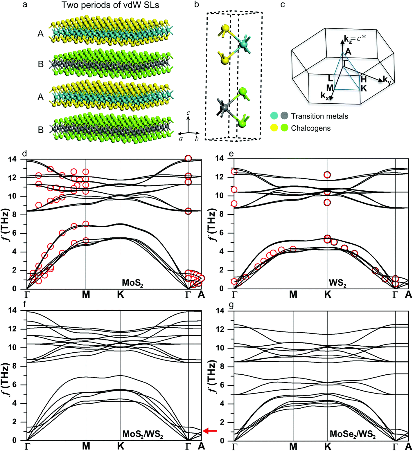 | ||
| Fig. 1 Crystal structures and phonon dispersions. (a) Schematic illustration of the AB-type vdW SL, showing two periods of the SL, (b) primitive unit cell and (c) Brillouin zone of the TMDC SLs MX2/M′X′2 (M/M′ = transition metals, X/X′ = chalcogens). Phonon dispersions of bulk (d) MoS2, (e) WS2, (f) MoS2/WS2 and (g) MoSe2/WS2 SLs. Calculations (solid lines) and experiments (red circles).50 The lowest six branches in the MoS2/WS2 SL exhibit distinct band splitting along the in-plane directions and band gaps (indicated by the red arrow) at the zone boundary of the cross-plane direction (Γ–A), both of which occur to a lesser degree in the MoSe2/WS2 SL. | ||
We first validate the accuracy of our calculations for bulk MoS2, WS2 and MoSe2. The fully relaxed lattice constants obtained from the vdW-DF functional deviate from experimental values by less than 1%.47–49Fig. 1d and e show the phonon dispersions of bulk MoS2 and WS2 (that of MoSe2 is given in ESI Fig. S2†), exhibiting good agreement with the data from inelastic neutron scattering.50 The in-plane longitudinal sound velocity is calculated to be 6730 m s−1 for bulk MoS2, which is close to our experimental value 7000 ± 40 m s−1 measured using ultrafast transient grating spectroscopy51 and previous ab initio predictions of 6500–6700 m s−1.52 All materials feature six dispersive phonon branches at the low-frequency range, which are separated from the relatively flat optical modes by a frequency gap. The gaps differ among the materials, with the largest one equaling 2.9 THz in WS2, MoSe2 lacking a gap, and that of MoS2 in between at 1.0 THz. The value of the gap is primarily due to the mass difference between the heavier transition metals and lighter chalcogens (Atomic mass (amu): Mo-95.94, W-183.84, S-32.065, Se-78.96), which dominate the vibrations of lower and higher branches, respectively (see ESI Fig. S3† for the density of states (DOS)). Another notable feature is the much lower cross-plane group velocities compared to the in-plane values, as indicated by the phonon dispersions along the Γ–A direction. This observation is expected considering the weak vdW interaction between layers.
The phonon dispersions of the MoS2/WS2 and MoSe2/WS2 SLs are presented in Fig. 1f and g, respectively. While they inherit many characteristics of those in bulk TMDCs, an obvious band splitting arises in both SLs due to the mass difference. For example, the large frequency gap featured in WS2 is occupied by three branches contributed by the MoSe2 layer in the MoSe2/WS2 SL. In particular, the lowest six branches in the MoS2/WS2 SL exhibit distinct band splitting along the in-plane directions and band gaps (indicated by the red arrow) at the zone boundary of the cross-plane direction (Γ–A), both of which occur to a lesser degree in the MoSe2/WS2 SL.
We then calculate the thermal conductivity κLversus temperature of bulk MoS2, MoSe2 and WS2 with the naturally occurring isotopic composition, as shown in Fig. 2a. The calculated values at 300 K are 102.6, 40.9 and 153.5 W m−1 K−1 for the in-plane thermal conductivity κIn and 5.1, 2.6 and 3.9 W m−1 K−1 for the cross-plane κCross, respectively. The experimental data are scattered for MoS2, falling in the range of 82–112 W m−1 K−1 and 2.0–4.8 W m−1 K−1 along the in- and cross-plane directions, respectively.53,54 A recent time-domain thermoreflectance measurement reported κIn = 35 W m−1 K−1 and κCross = 2.6 W m−1 K−1 for MoSe2.54 For WS2, the measured in-plane data are close to 124 W m−1 K−1 while the cross-plane values vary from 1.7 to 2.9 W m−1 K−1.54,55 The decreasing orders WS2 > MoS2 > MoSe2 for κIn and MoS2 > WS2 > MoSe2 for κCross from our calculations are consistent with measurements54 and prior ab initio calculations.52 We find that the impurity scattering more strongly suppresses the κIn due to the significant contribution of higher frequency modes along this crystal plane, possibly explaining why our results agree better with the κCross reported by Jiang et al.54 (see ESI Note 2† for details).
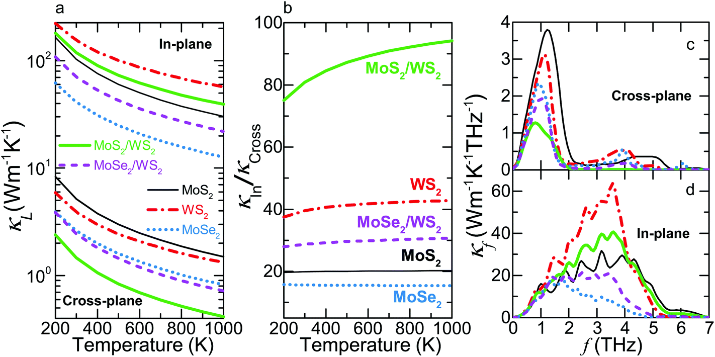 | ||
| Fig. 2 κ L and its spectral contribution of MoS2, WS2, MoSe2, MoS2/WS2 and MoSe2/WS2 crystals. (a) Cross-plane (bottom) and in-plane (top) κLversus temperature. (b) Thermal anisotropy, κIn/κCross, versus temperature. (c) Cross-plane and (d) in-plane thermal conductivity contribution κfversus frequency. The thermal anisotropy ratio of the MoS2/WS2 SL is enhanced by a factor of ∼2 at different temperatures due to the mainly preserved κIn and substantially reduced κCross while that of the MoSe2/WS2 SL is decreased by ∼20%. | ||
We next calculate the thermal conductivity of the MoS2/WS2 and MoSe2/WS2 SLs. Since MoS2 has much higher κIn and κCross than those of MoSe2, classical effective medium theories would predict that a composite with MoS2 would have higher κL than one with MoSe2. However, our calculation shows that the MoS2/WS2 SL has much lower κCross and larger thermal anisotropy than those of the MoSe2/WS2 SL. As shown in Fig. 2a, the MoS2/WS2 SL exhibits the lowest κCross over the entire temperature range, which is substantially reduced compared to the corresponding values of either constituent material. However, the κCross of the MoSe2/WS2 SL is very close to that of MoSe2, especially at low temperatures. For example, with respect to the lower value of the corresponding bulk materials, the κCross of the MoS2/WS2 and MoSe2/WS2 SLs is reduced by 62.4% and 6.7% at 300 K, respectively.
In contrast to the reduction of the κCross, the κIn of both SLs lies in between those of corresponding bulk materials. We also note that the κIn of the MoS2/WS2 SL is closer to the average value of the corresponding bulk constituents, lower by 7.7% at 300 K, whereas that of the MoSe2/WS2 SL has a value 32.1% lower. Due to the different variation of κIn and κCross from those of the bulk materials, both SLs exhibit altered thermal anisotropy ratios κIn/κCross, as illustrated in Fig. 2b. In the present work, we evaluate the variation of thermal anisotropy in SLs using the constituent material with larger thermal anisotropy ratio as the reference (WS2 for both SLs). The thermal anisotropy ratio of the MoS2/WS2 SL is enhanced by a factor of ∼2 while that of the MoSe2/WS2 SL is decreased by ∼20% throughout our temperature range.
To understand the unusual thermal anisotropy in these SLs, we first plot the thermal conductivity distribution κfversus frequency at 300 K in Fig. 2c and d. We observe that the cross-plane κf is mainly contributed by phonons within a narrow frequency range (f < ∼2 THz) for each material. For both SLs, the reduction of the cross-plane κf contribution with respect to those of the bulk counterparts decreases as f approaches zero. Above this low-frequency range, the κf of the MoS2/WS2 SL is substantially suppressed and becomes negligible above 2.1 THz while that of the MoSe2/WS2 SL is very close to the value of MoSe2 above 1.2 THz.
Along the in-plane direction, the major κf contribution comes from a broader frequency range (up to ∼5 THz) for all materials, as shown in Fig. 2d. Similarly, the in-plane κf of the two SLs almost overlaps with that of corresponding bulk crystals below ∼1 THz. Above this range, the κf of both SLs lies in between that of constituent materials although the κf of the MoSe2/WS2 SL is significantly lower than the average value of its constituent materials. Furthermore, the lowest six branches contribute more than 94% of the total κIn and κCross in each material.
These calculations indicate that the origin of the increased thermal anisotropy in the MoS2/WS2 SL lies in the mainly preserved and decreased contribution of modes with frequency less than around 7 THz along the in- and cross plane directions, respectively. This difference among directions must be due to changes in either harmonic properties such as group velocities and phonon scattering phase space or the strength of anharmonic coupling determined by the magnitude of the cubic force constants.
We first probe the role of scattering phase space and anharmonicity by examining the lifetimes of the MoS2/WS2 SL. We find that the lifetimes of the lowest six branches can be divided into two sets of three, for which each have lifetimes similar to either those of bulk MoS2 and WS2. In Fig. 3a and b, we show the lifetimes of the first transverse acoustic branch B1 (from the WS2 layer) and the highest low-lying branch B6 (from the MoS2 layer), as typical examples. This splitting of the lifetimes between each constituent material arises from the splitting of previously degenerate phonon modes, as shown in Fig. 3c. Due to the bilayer structure of the unit cell, the vibrations of the MoS2 and WS2 layers separately contribute to three branches, which, importantly, almost overlap with those in bulk MoS2 and WS2. Therefore, the κIn of the SLs approaches the average value of bulk constituent materials considering that the individual κL contributions of the six branches are comparable.
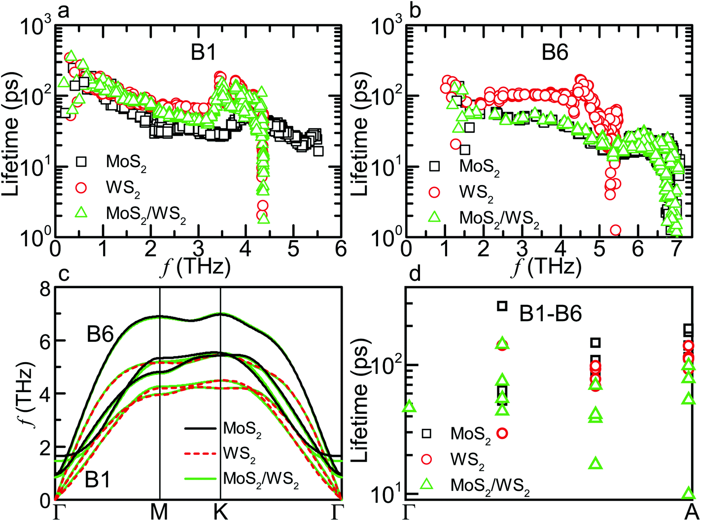 | ||
| Fig. 3 Phonon lifetimes and dispersions in MoS2, WS2 and MoS2/WS2 crystals. Lifetimes of (a) the first transverse acoustic (B1) and (b) highest low-lying (B6) branches. (c) Phonon dispersions of the six low-lying branches B1–B6 along the in-plane directions in the MoS2/WS2 SL, along with three separate branches from bulk WS2 and MoS2, respectively. The splitting of the lifetimes between each constituent material arises from the splitting of phonon dispersions. (d) Lifetimes of B1–B6 along the Γ–A direction. The relatively suppressed lifetimes of the MoS2/WS2 SL near the zone edge have only a minor contribution to the reduction of the total κCross. | ||
The splitting of phonon dispersions changes phonon scattering channels and thus lifetimes, which depend on the frequency range of acoustic (including the six low-lying branches as they all have acoustic-like behavior) and optical branches. As shown in Fig. 3a and b, some lifetimes of B1 are relatively smaller than those in bulk WS2 while most lifetimes of B6 are very close to the corresponding values in bulk MoS2. The former behavior is mainly due to the enhanced aoo scattering, or scattering between one acoustic and two optical phonons, which is the dominant process for these modes of B1. For example, 85.3% of the scattering rate for the mode M1 (q = [0, 8/27, 0], 2.9 THz) from B1 is contributed by aoo scattering in the MoS2/WS2 SL, which is larger by 14.5% with respect to that in WS2. The enhancement can be explained by the widening of optical spectrum, from 4.3 THz in WS2 to 5.4 THz in the MoS2/WS2 SL, resulting in more aoo scattering channels. In contrast, the widths of acoustic and optical spectra in this SL are very close to those in MoS2, resulting in similar scattering rates of B6. For the MoSe2/WS2 SL, the width of optical spectrum further increases to 7.6 THz, which thus causes stronger enhancement of aoo scattering for phonon modes contributed by WS2 layers. Meanwhile, the appearance of three branches in the band gap allows more aao channels. Consequently, the κIn of the MoSe2/WS2 SL is further lowered from the average value of corresponding bulk ones.
The large thermal anisotropy of the SLs is due to mainly preserved κIn, the origin of which is discussed above, and due to reduced κCross. We now examine if the lifetimes of phonons along the Γ–A direction can explain this reduction in κCross. Fig. 3d shows that, as the q vector approaches the zone edge, the lifetimes of the MoS2/WS2 SL become relatively smaller than those in bulk MoS2 and WS2. However, recalculating κCross of WS2 using these lifetimes leads to only a decrease of 0.23 W m−1 K−1, accounting for 9.6% of the overall reduction (from 3.9 in WS2 to 1.5 W m−1 K−1 in the MoS2/WS2 SL). Therefore, the major reduction of the κCross must result from alterations to the phonon dispersion.
Fig. 4a and b show the z-component group velocities normalized by the magnitude of the group velocity of the second transverse acoustic (B2) and the B6 branches in the WS2, MoS2/WS2 and MoSe2/WS2 crystals. The corresponding values in MoS2 and MoSe2 are comparable to or higher than those in WS2. Clearly, the MoS2/WS2 SL has substantially smaller normalized cross-plane group velocities compared to WS2 except for the low-frequency range, where the group velocity vectors of a few modes lie directly along the cross-plane direction. Above ∼2 THz, the z-component of the group velocity is only less than 3% of the magnitude of overall group velocities for most phonons in the MoS2/WS2 SL, and those with larger z-components at the high-frequency range also have small absolute group velocities, explaining the corresponding negligible κL contribution. Conversely, there is no significant suppression in the normalized z-component group velocities of the MoSe2/WS2 SL.
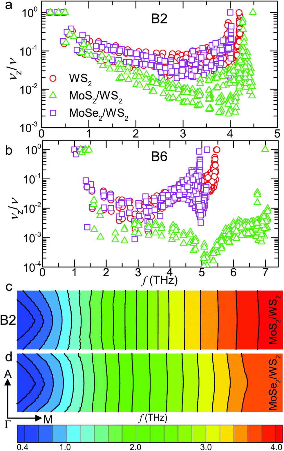 | ||
| Fig. 4 Normalized cross-plane group velocities and isoenergy surfaces. Cross-plane group velocities normalized by the magnitude of group velocities of (a) the second transverse acoustic (B2) and (b) the B6 branches for the WS2, MoS2/WS2 and MoSe2/WS2 crystals. Isoenergy surfaces of B2 in the A–Γ–M plane for (c) MoS2/WS2 and (d) MoSe2/WS2 SLs. The substantially smaller normalized cross-plane group velocities of the MoS2/WS2 SL arise from phonon focusing effects, as indicated by the smaller curvatures of the isoenergy surfaces. | ||
We further reveal the phonon focusing effect by visualizing the isoenergy surfaces of B2 in the A–Γ–M plane for both SLs, as plotted in Fig. 4c and d. The comparison clearly indicates smaller curvatures of the isoenergy surfaces in the MoS2/WS2 SL. In the middle range (2–3 THz), the isoenergy surfaces of the MoS2/WS2 SL are almost completely flat, resulting in phonon focusing along the in-plane direction. Above 3 THz, the MoSe2/WS2 SL exhibits dispersive isoenergy surfaces, in contrast to the relatively flat ones in the MoS2/WS2 SL. The flattening of the isoenergy surfaces thus leads to a decrease in the slope of the surface and hence the cross-plane group velocities, increasing the thermal anisotropy. A similar effect has also been reported in graphite by tuning the in-plane/cross-plane bonding strength, resulting in a negative correlation between the bonding strength and κL along the orthogonal direction.56
We now seek to clarify the physical mechanisms for the flattening of the isoenergy surfaces. Early works suggested that phonon group velocity vectors are preferentially focused along the crystalline directions with larger elastic constants.57 However, elastic anisotropy cannot explain the enhanced thermal anisotropy in the MoS2/WS2 SL, which has a ratio of elastic constants C11/C33 = 4.9, compared to 4.5 for MoS2 and 5.1 for WS2 from ab initio calculations.
Zone folding effects have been used to explain the decrease of cross-plane group velocities in SLs.58–61 The present SLs have approximately the same Brillouin zone size as bulk TMDCs, suggesting that zone-folding does not occur. However, if we observe that approximating the three atoms in each layer of the unit cell as an equivalent atom simplifies bulk TMDCs to parallel monatomic chains, while those of the SLs are diatomic chains, the Brillouin zone of the SLs must be folded once along the cross-plane direction. As a result, flattened bands and band gaps are expected to appear near the zone edges where the Bragg reflection condition is satisfied.59
These features are indeed observed in the dispersion of the MoS2/WS2 SL along the Γ–A direction, as shown in Fig. 1f. Due to the Bragg reflection, the group velocity vanishes near the zone edge. In addition, anticrossing effects occur inside the zone due to Bragg reflections60 (ESI Fig. S4†), further suppressing the cross-plane group velocities. The band gaps at zone edges and anticrossings yield sharp peaks in the DOS projected along the z axis for the SL, a unique feature distinct from bulk TMDCs (ESI Fig. S5†). Furthermore, the optical phonons of the MoS2 and WS2 layers have no common frequencies and thus become localized, resulting in flat dispersions. Due to the negligible κL contribution of these branches, this effect has little influence on the thermal anisotropy of TMDC SLs. However, it may cause significant enhancement of thermal anisotropy of vdW materials for which these modes contribute, such as for SnSe and SnS.62
In contrast, the MoSe2/WS2 SL shows no clear band gaps along the Γ–A direction, as shown in Fig. 1g. The major difference between the two SLs is the mass ratio of neighboring layers, being 1.55 for the MoS2/WS2 SL compared to 1.02 for the MoSe2/WS2 SL. As in the simple diatomic chain model, the frequency gap vanishes as the masses become equal. We validate this explanation by computing how phonon dispersions change as the mass of one of the bilayers is varied while keeping the same force constants as in MoS2. Modifying the mass of Mo or S significantly alters the magnitude of the band gaps at the zone edge (ESI Fig. S6†).
A key requirement for coherent manipulation of phonons is that the coherence length must be much longer than the imposed periodicity. Our calculation shows that for the MoS2/WS2 SL, phonons with MFPs longer than 200 nm contribute 88% to the κCross, indicating that most heat is indeed carried by phonons with coherence lengths far exceeding SL periodicity of 12.42 Å (ESI Fig. S7†). As the period increases, scattering events will cause decoherence, preventing interference and thereby leading to the effective medium limit. For the MoSe2/WS2 SL, although phonons with MFPs longer than 200 nm contribute 82% to the κCross, coherent interference has little effect on the thermal transport due to the negligible mass difference between layers.
The thermal anisotropy in TMDC SLs can be further enhanced by additional zone folding. For example, we construct two representative SLs with four atomic layers in each period: WS2/2MoS2/WSe2 (mass ratio = 1:0.65:0.65:1.38) and WS2/2MoSe2/WSe2 (mass ratio = 1:1.02:1.02:1.38), producing a thermal anisotropy of 176 and 50 at 300 K, respectively, as shown in Fig. 5. The large thermal anisotropy of the former SL is comparable to that (100–300) of high-quality graphite.63 Meanwhile, its κCross decreases to 0.4 W m−1 K−1, which is close to that of amorphous polymers (∼0.35 W m−1 K−1 for bulk polyethylene).63 These results agree well with our expectation considering the dominant role of band splitting and phonon focusing (ESI Fig. S8†).
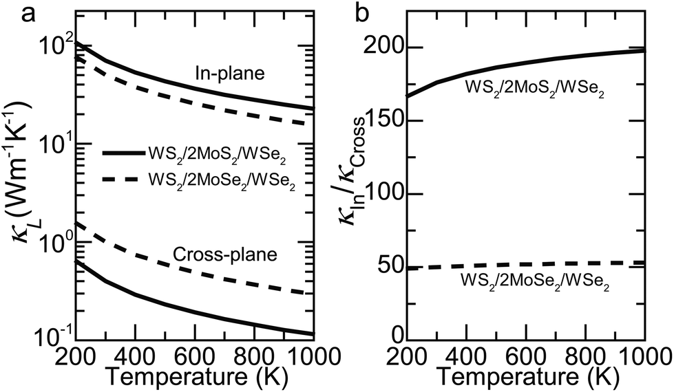 | ||
| Fig. 5 Coherent manipulation of thermal transport for SLs with four atomic layers in each period (WS2/2MoS2/WSe2 with mass ratio = 1:0.65:0.65:1.38 and WS2/2MoSe2/WSe2 with mass ratio = 1:1.02:1.02:1.38). (a) Cross-plane (bottom) and in-plane (top) κL with respect to temperature. (b) Thermal anisotropy, κIn/κCross, versus temperature. The thermal anisotropies of the WS2/2MoS2/WSe2 SL are substantially further enhanced by additional zone folding. | ||
In this work, the very similar lattice structures of different TMDCs result in band splitting and hence mainly preserved κIn, leading to enhanced thermal anisotropy. Constructing vdW HTs as a versatile strategy to enhance thermal anisotropy will benefit designing efficient thermal management of electronics and exploring extreme values of thermal conductivity such as low values for thermoelectrics. We expect that for vdW SLs consisting of materials with dissimilar crystal structures, a more dramatic modification of phonon scattering phase space may have stronger influence on thermal conductivity along different crystallographic directions. For instance, an unusual enhancement of thermal conductivity of the short-period Si/Ge SL compared to those of both its constituents has been observed due to the suppressed scattering of acoustic phonons by optical phonons.26 For a given vdW SL, twisting plane rotation angles can further manipulate the vibrational spectrum and scattering strength.64
It should be noted that the modification of phonon dispersions in vdW SLs also depends on weak vdW interactions, which allow for the simplification of diatomic chain models. Such a treatment may fail for traditional short-period SLs coupled via strong covalent bonds, in which atomic interactions beyond nearest neighbors are not negligible. Therefore, the strength of vdW interactions, which can be tuned by for example applying pressure,65 offers another degree of freedom for the design of thermal properties using vdW SLs.
IV. Conclusions
In summary, we report an ab initio study of coherent phonons and thermal transport in vdW SLs as the periodicity approaches the atomically thin limit. Our calculations show that these materials achieve novel thermal properties such as large thermal anisotropies approaching 200 and ultralow cross-plane thermal conductivities comparable to those of amorphous materials. Further coherent control of the thermal transport may be achieved using vdW SLs composed of atomic layers of diverse lattice structures, leading to strongly modified phonon scattering phase space and anharmonicity. Our study indicates a promising route to experimentally realize solids with thermal properties that do not occur naturally in atomically precise vdW superlattices.Author contributions
R. G. performed the calculations. All authors contributed to the analysis and discussion of the results. R. G. and A. J. M. wrote the manuscript.Conflicts of interest
There are no conflicts to declare.Acknowledgements
This work was supported by the “GIST-Caltech Research Collaboration” Project through a grant provided by Gwangju Institute of Science and Technology in 2017 and the DARPA MATRIX program under Grant No. HR0011-15-2-0039.References
- A. K. Geim and I. V. Grigorieva, Nature, 2013, 499, 419–425 CrossRef PubMed.
- Y. Liu, N. O. Weiss, X. Duan, H.-C. Cheng, Y. Huang and X. Duan, Nat. Rev. Mater., 2016, 1, 16042 CrossRef.
- W. J. Yu, Z. Li, H. Zhou, Y. Chen, Y. Wang, Y. Huang and X. Duan, Nat. Mater., 2013, 12, 246–252 CrossRef PubMed.
- W. Yang, G. Chen, Z. Shi, C.-C. Liu, L. Zhang, G. Xie, M. Cheng, D. Wang, R. Yang and D. Shi, Nat. Mater., 2013, 12, 792–797 CrossRef PubMed.
- T. Georgiou, R. Jalil, B. D. Belle, L. Britnell, R. V. Gorbachev, S. V. Morozov, Y.-J. Kim, A. Gholinia, S. J. Haigh and O. Makarovsky, Nat. Nanotechnol., 2013, 8, 100–103 CrossRef PubMed.
- L. Britnell, R. V. Gorbachev, R. Jalil, B. D. Belle, F. Schedin, A. Mishchenko, T. Georgiou, M. I. Katsnelson, L. Eaves, S. V. Morozov, N. M. Peres, J. Leist, A. K. Geim, K. S. Novoselov and L. A. Ponomarenko, Science, 2012, 335, 947–950 CrossRef PubMed.
- W. Zhang, C. P. Chuu, J. K. Huang, C. H. Chen, M. L. Tsai, Y. H. Chang, C. T. Liang, Y. Z. Chen, Y. L. Chueh, J. H. He, M. Y. Chou and L. J. Li, Sci. Rep., 2014, 4, 3826 CrossRef PubMed.
- R.-J. Shiue, Y. Gao, Y. Wang, C. Peng, A. D. Robertson, D. K. Efetov, S. Assefa, F. H. Koppens, J. Hone and D. Englund, Nano Lett., 2015, 15, 7288–7293 CrossRef PubMed.
- W. J. Yu, Y. Liu, H. Zhou, A. Yin, Z. Li, Y. Huang and X. Duan, Nat. Nanotechnol., 2013, 8, 952–958 CrossRef PubMed.
- S. Bertolazzi, D. Krasnozhon and A. Kis, ACS Nano, 2013, 7, 3246–3252 CrossRef PubMed.
- M. S. Choi, G.-H. Lee, Y.-J. Yu, D.-Y. Lee, S. H. Lee, P. Kim, J. Hone and W. J. Yoo, Nat. Commun., 2013, 4, 1624 CrossRef PubMed.
- F. Withers, O. D. Pozo-Zamudio, A. Mishchenko, A. Rooney, A. Gholinia, K. Watanabe, T. Taniguchi, S. Haigh, A. Geim and A. Tartakovskii, Nat. Mater., 2015, 14, 301–306 CrossRef PubMed.
- H. Fang, C. Battaglia, C. Carraro, S. Nemsak, B. Ozdol, J. S. Kang, H. A. Bechtel, S. B. Desai, F. Kronast, A. A. Unal, G. Conti, C. Conlon, G. K. Palsson, M. C. Martin, A. M. Minor, C. S. Fadley, E. Yablonovitch, R. Maboudian and A. Javey, Proc. Natl. Acad. Sci. U. S. A., 2014, 111, 6198–6202 CrossRef PubMed.
- B. Hunt, J. D. Sanchez-Yamagishi, A. F. Young, M. Yankowitz, B. J. LeRoy, K. Watanabe, T. Taniguchi, P. Moon, M. Koshino, P. Jarillo-Herrero and R. C. Ashoori, Science, 2013, 340, 1427–1430 CrossRef PubMed.
- C. Dean, L. Wang, P. Maher, C. Forsythe, F. Ghahari, Y. Gao, J. Katoch, M. Ishigami, P. Moon and M. Koshino, Nature, 2013, 497, 598–602 CrossRef PubMed.
- L. Ponomarenko, R. Gorbachev, G. Yu, D. Elias, R. Jalil, A. Patel, A. Mishchenko, A. Mayorov, C. Woods and J. Wallbank, Nature, 2013, 497, 594–597 CrossRef PubMed.
- G. Chen, Nanoscale energy transport and conversion, Oxford University Press, New York, 2005 Search PubMed.
- C. J. Vineis, A. Shakouri, A. Majumdar and M. G. Kanatzidis, Adv. Mater., 2010, 22, 3970–3980 CrossRef PubMed.
- T. Luo and G. Chen, Phys. Chem. Chem. Phys., 2013, 15, 3389–3412 RSC.
- D. G. Cahill, P. V. Braun, G. Chen, D. R. Clarke, S. Fan, K. E. Goodson, P. Keblinski, W. P. King, G. D. Mahan and A. Majumdar, Appl. Phys. Rev., 2014, 1, 011305 Search PubMed.
- M. N. Luckyanova, J. Garg, K. Esfarjani, A. Jandl, M. T. Bulsara, A. J. Schmidt, A. J. Minnich, S. Chen, M. S. Dresselhaus, Z. Ren, E. A. Fitzgerald and G. Chen, Science, 2012, 338, 936–939 CrossRef PubMed.
- J. Ravichandran, A. K. Yadav, R. Cheaito, P. B. Rossen, A. Soukiassian, S. Suresha, J. C. Duda, B. M. Foley, C.-H. Lee and Y. Zhu, Nat. Mater., 2014, 13, 168–172 CrossRef PubMed.
- J. Maire, R. Anufriev, R. Yanagisawa, A. Ramiere, S. Volz and M. Nomura, Sci. Adv., 2017, 3, e1700027 CrossRef PubMed.
- M. Maldovan, Nature, 2013, 503, 209–217 CrossRef PubMed.
- M. Maldovan, Nat. Mater., 2015, 14, 667–674 CrossRef PubMed.
- J. Garg, N. Bonini and N. Marzari, Nano Lett., 2011, 11, 5135–5141 CrossRef PubMed.
- J. Garg and G. Chen, Phys. Rev. B: Condens. Matter, 2013, 87, 140302 CrossRef.
- X. Mu, T. Zhang, D. B. Go and T. Luo, Carbon, 2015, 83, 208–216 CrossRef.
- C. da Silva, F. Saiz, D. A. Romero and C. H. Amon, Phys. Rev. B: Condens. Matter, 2016, 93, 125427 CrossRef.
- B. Latour and Y. Chalopin, Phys. Rev. B: Condens. Matter, 2017, 95, 214310 CrossRef.
- Z. Zhang, P. Chen, X. Duan, K. Zang, J. Luo and X. Duan, Science, 2017, 357, 788–792 CrossRef PubMed.
- K. Chiu, K. Huang, C. Chen, Y. Lai, X. Zhang, E. Lin, M. Chuang, J. Wu and Y. Lee, Adv. Mater., 2018, 30, 1704796 CrossRef PubMed.
- P. Chen, N. Katcho, J. Feser, W. Li, M. Glaser, O. Schmidt, D. G. Cahill, N. Mingo and A. Rastelli, Phys. Rev. Lett., 2013, 111, 115901 CrossRef PubMed.
- B. Liu, J. A. Baimova, C. D. Reddy, A. W.-K. Law, S. V. Dmitriev, H. Wu and K. Zhou, ACS Appl. Mater. Interfaces, 2014, 6, 18180–18188 Search PubMed.
- B. Liu, F. Meng, C. D. Reddy, J. A. Baimova, N. Srikanth, S. V. Dmitriev and K. Zhou, RSC Adv., 2015, 5, 29193–29200 RSC.
- Z. Ding, Q.-X. Pei, J.-W. Jiang, W. Huang and Y.-W. Zhang, Carbon, 2016, 96, 888–896 CrossRef.
- Z. Yan, L. Chen, M. Yoon and S. Kumar, Nanoscale, 2016, 8, 4037–4046 RSC.
- D. Broido, M. Malorny, G. Birner, N. Mingo and D. Stewart, Appl. Phys. Lett., 2007, 91, 231922 CrossRef.
- X. Wang and B. Huang, Sci. Rep., 2014, 4, 6399 CrossRef PubMed.
- A. Ward, D. Broido, D. A. Stewart and G. Deinzer, Phys. Rev. B: Condens. Matter, 2009, 80, 125203 CrossRef.
- L. Lindsay, D. Broido and T. Reinecke, Phys. Rev. Lett., 2012, 109, 095901 CrossRef PubMed.
- W. Li and N. Mingo, Phys. Rev. B: Condens. Matter, 2014, 90, 094302 CrossRef.
- R. Guo, X. Wang and B. Huang, Sci. Rep., 2015, 5, 7806 CrossRef PubMed.
- N. Shulumba, O. Hellman and A. J. Minnich, Phys. Rev. B: Condens. Matter, 2017, 95, 014302 CrossRef.
- G. Kresse and J. Furthmuller, Phys. Rev. B: Condens. Matter, 1996, 54, 11169–11186 CrossRef.
- K. Kang, K.-H. Lee, Y. Han, H. Gao, S. Xie, D. A. Muller and J. Park, Nature, 2017, 550, 23905 CrossRef PubMed.
- V. Kalikhman, Izv. Akad. Nauk SSSR, Neorg. Mater., 1983, 19, 1060–1065 Search PubMed.
- K. Bronsema, J. D. Boer and F. Jellinek, Z. Anorg. Allg. Chem., 1986, 540, 15–17 CrossRef.
- W. J. Schutte, J. L. D. Boer and F. Jellinek, J. Solid State Chem., 1987, 70, 207–209 CrossRef.
- N. Wakabayashi, H. Smith and R. Nicklow, Phys. Rev. B: Solid State, 1975, 12, 659 CrossRef.
- T. Kim, D. Ding, J.-H. Yim, Y.-D. Jho and A. J. Minnich, APL Mater., 2017, 5, 086105 CrossRef.
- D. O. Lindroth and P. Erhart, Phys. Rev. B: Condens. Matter, 2016, 94, 115205 CrossRef.
- J. Liu, G.-M. Choi and D. G. Cahill, J. Appl. Phys., 2014, 116, 233107 CrossRef.
- P. Jiang, X. Qian, X. Gu and R. Yang, Adv. Mater., 2017, 29, 1701068 CrossRef PubMed.
- A. Pisoni, J. Jacimovic, R. Gal, B. Nfrdi, H. Berger, Z. Rvay and L. Forr, Scr. Mater., 2016, 114, 48–50 CrossRef.
- Z. Wei, Y. Chen and C. Dames, Appl. Phys. Lett., 2013, 102, 011901 CrossRef.
- B. Taylor, H. Maris and C. Elbaum, Phys. Rev. Lett., 1969, 23, 416 CrossRef.
- C. Colvard, T. Gant, M. Klein, R. Merlin, R. Fischer, H. Morkoc and A. Gossard, Phys. Rev. B: Condens. Matter, 1985, 31, 2080 CrossRef.
- D. Hurley, S. Tamura, J. Wolfe and H. Morkoc, Phys. Rev. Lett., 1987, 58, 2446 CrossRef PubMed.
- S. Tamura and J. Wolfe, Phys. Rev. B: Condens. Matter, 1987, 35, 2528 CrossRef.
- M. Simkin and G. Mahan, Phys. Rev. Lett., 2000, 84, 927–930 CrossRef PubMed.
- R. Guo, X. Wang, Y. Kuang and B. Huang, Phys. Rev. B: Condens. Matter, 2015, 92, 115202 CrossRef.
- Y. S. Touloukian, Thermophysical properties of matter, IFI/Plenum, New York, 1970 Search PubMed.
- H. Li, H. Ying, X. Chen, D. L. Nika, A. I. Cocemasov, W. Cai, A. A. Balandin and S. Chen, Nanoscale, 2014, 6, 13402–13408 RSC.
- X. Meng, T. Pandey, S. Fu, J. Yang, J. Jeong, K. Chen, A. Singh, F. He, X. Xu and A. K. Singh, 2017, arXiv preprint arXiv:1708.03849.
Footnote |
| † Electronic supplementary information (ESI) available. See DOI: 10.1039/C8NR02150C |
| This journal is © The Royal Society of Chemistry 2018 |