
 Open Access Article
 This Open Access Article is licensed under a
 Creative Commons Attribution 3.0 Unported Licence
Focused ion beam milling of self-assembled magnetic superstructures: an approach to fabricate nanoporous materials with tunable porosity†
Verner
Håkonsen
 a,
Gurvinder
Singh
bc,
Jianying
He
a and
Zhiliang
Zhang
*a
a,
Gurvinder
Singh
bc,
Jianying
He
a and
Zhiliang
Zhang
*a
aNTNU Nanomechanical Lab, Department of Structural Engineering, Norwegian University of Science and Technology (NTNU), Trondheim 7491, Norway. E-mail: zhiliang.zhang@ntnu.no
bDepartment of Materials Science and Engineering, Norwegian University of Science and Technology (NTNU), Trondheim 7491, Norway
cSchool of Aerospace, Mechanical and Mechatronic Engineering, University of Sydney, Sydney, NSW 2008, Australia
First published on 19th September 2018
Abstract
Fabricating nanoporous materials with tunable pore sizes while keeping the freedom of materials choice, is an active area of research because of its practical relevance in a wide range of applications. Here, we demonstrate a novel approach for the first time based on focused ion beam milling of self-assembled superstructures made from nanoparticles. The interaction of the ion beam at different voltages with the self-assembled superstructures, leads to nanoporous materials with the possibility to tune the porosity. The porosity in the superstructures evolves as constituent nanoparticles merge together as a results of combined milling and melting.
Conceptual insightsSelf-assembly, an approach inspired by nature itself, is an attractive route to fabricate functional materials with enhanced and collective properties from nanoscale building blocks, such as molecules and nanoparticles. Although, a significant progress has been made to develop self-assembled materials from various nanoscale building blocks, creating advanced materials with unusual properties from pre-designed self-assembled materials offers notable opportunities which remain unexplored to date. This includes the behaviour of self-assembled nanoparticle-based superstructures under the influence of ion beam exposure. Here, we demonstrate how focused ion beam milling of self-assembled magnetic superstructures can be used as an approach to fabricate nanoporous materials with tunable porosity. Overall, this discovery introduces a novel alternative methodology to fabricate three-dimensional nanoporous materials from pre-designed self-assembled materials constituted from inorganic nanoparticles, thus advancing the field of nanoporous materials. Nanoporous materials exhibit unique properties due to their large specific surface area, and are thus recognized as potential candidates for the use in a wide range of applications. Our approach offers several advantages over existing strategies, such as a great flexibility in terms of materials choice, fine control over the porosity via ion beam voltage and shape of nanoparticles, local fabrication of nanopores, and no use of toxic chemicals. |
Introduction
Designing novel superstructured materials via self-assembly of nanoparticles is a promising approach because of its versatility in fabricating composite two- (2D) and three-dimensional (3D) materials from nanoparticles of different sizes, shapes and materials.1–3 Self-assembled nanoparticles exhibit extraordinary and novel physical properties due to the synergy between their individual counterparts.4 The main advantage in using the self-assembly approach to fabricate advanced nanomaterials, is the large degree of freedom in the control of structure and morphology, and subsequently their properties, due to the intrinsic and extrinsic forces involved in the self-assembly of nanoparticles.5 While significant progress has been made in the understanding of self-assembled materials fabrication, the behavior of these self-assembled materials under ion beam exposure has remained unexplored to date. Here, we fabricate self-assembled superstructures in different morphologies from magnetic nanoparticles of different shapes, and investigate their interaction with a Ga+-ion beam by means of the focus ion beam (FIB) milling technique. We find that the controlled exposure of the ion beam to the self-assembled superstructures leads to the evolution of 3D nanoporous materials. Our presented approach thus represents an alternative novel route to fabricate nanoporous materials.In the literature, different synthetic strategies have been proposed for fabricating (nano)porous materials. Among these, dealloying approaches involving the selective leaching of one component from a precursor alloy via electrochemical or metallic melt,6–9 as well as hard- or soft-template-based strategies,10–12 have been extensively investigated. In addition, nanoparticle aggregates have also previously been utilized as a method to obtain porous structures,13 however, the resulting network does not have a distinct backbone, and the only way to truly control the porosity is by invoking ordering and changing the particle size, making this method cumbersome. In our approach, the key step is the a priori formation of ordered nanoparticle-based superstructures, acting as an imperative starting point for ion beam exposure. As the nanoparticle-based superstructures are exposed to the focused ion beam, the nanoparticles are not only subjected to milling, but also melting, which facilitates the formation of porous materials. Here, our fabrication approach based on FIB milling offers several advantages compared to previous strategies; independent of materials choice, fine control over pore size distribution and interconnected pore network via the control of ion beam acceleration voltage and shape of nanoparticles, no use of toxic chemicals, and the possibility to locally fabricate porous structures. Furthermore, the morphology of superstructures can also be altered (from complete sample coverage to various geometries) by performing self-assembly under external stimuli (magnetic field, light),14,15 allowing us to also fabricate nanoporous materials in different morphologies. Nanoporous materials are very promising candidates for practical applications, because these materials possess an interconnected porous network and nanosized walls, overall giving rise to a large surface area with many functional sites. This leads to unique chemical and physical properties compared to their nanostructured (non-porous) and bulk material counterparts.16–18 The potential applications of nanoporous materials are widespread, and include tissue engineering,19,20 drug delivery,21 microfluidics,22 catalysis,23,24 separation,23,24 energy storage and conversion,24,25 sensing devices,24 and anti-icing.26,27
Results and discussion
In this study, cobalt ferrite (CoFe2O4) nanoparticles in spherical (diameter ∼ 10 ± 1 nm) and cubic (edge length ∼ 10 ± 1 nm) shape (transmission electron microscopy (TEM) images in Fig. 1a), were used as the material of choice, and synthesized by thermal decomposition of a metal-oleate precursor (Experimental methods, ESI†).28 Subsequently, the self-assembly approach at the liquid–air interface was used to form ordered superstructures. A hexane solution of nanoparticles (∼8.5 mg mL−1) was added and spread out at the diethylene glycol interface in a polyethylene well. A slow evaporation of hexane in a closed environment facilitated the formation of ordered superstructures at the interface, which were thereafter transferred onto a silicon substrate (scheme in Fig. 1b). The spherical nanoparticles typically self-assembled into hexagonal closed packed superstructures (Fig. 1c and d), whereas cubic nanoparticles formed supercubic structures in which the nanocubes in the interior were packed in a cubic arrangement (Fig. 1e and f). The difference in the final morphology of superstructures originates from the fact that spherical and cubic nanoparticles crystallize into hexagonal and simple cubic lattices (fast Fourier transforms (FFTs) shown in the insets of Fig. 1d and f), respectively, in 3D to gain accessible volume, and thus entropy.5 A monolayer of oleic acid surfactant coating the nanoparticle surface acted as a stabilizer in the self-assembly process and provided a spacing, in this case ∼2–3 nm, between nearest neighbours in the assembled superstructures (i.e. nanocomposites). After the bottom-up self-assembly process, the superstructures were subjected to top-down FIB milling with controllable ion beam acceleration voltage and dose, to yield porous structures with tunable porosity from the nanoscale to the submicron-scale (Fig. 1b).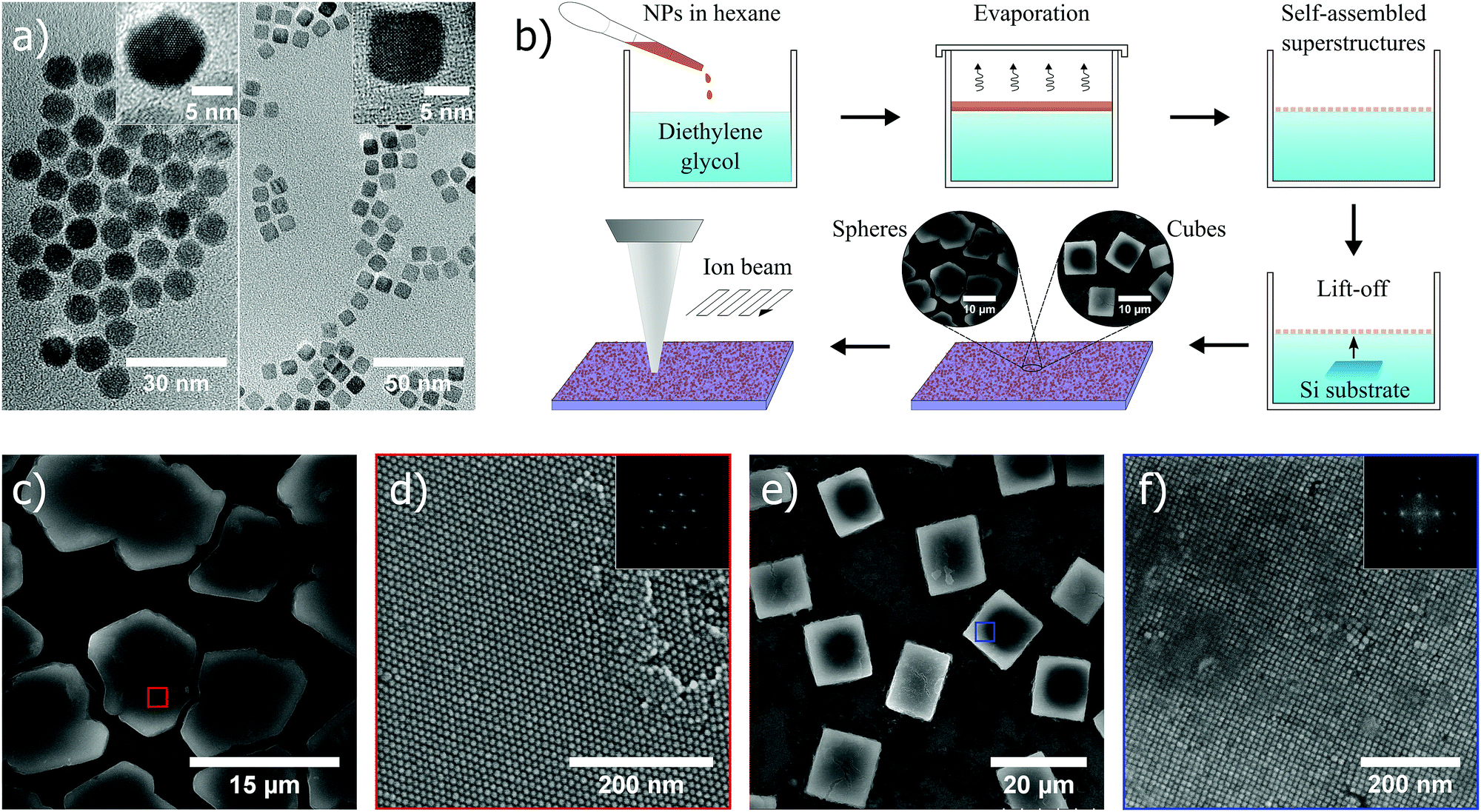 | ||
| Fig. 1 Fabrication process of porous structures from nanoparticle-based ordered superstructures. (a) TEM micrographs showing individual 10 nm nanospheres and nanocubes used in superstructure fabrication. (b) Fabrication of porous structures starts with superstructure fabrication by the liquid–air interface approach. Nanoparticles (NPs) dispersed in hexane self-assemble into ordered superstructures at the liquid–air interface as the solvent evaporates, and are subsequently transferred onto a Si substrate through lift-off. Thereafter the superstructures are subjected to FIB exposure. The SEM micrographs in (c–f) show self-assembled magnetic superstructures built up from nanospheres (c and d) and nanocubes (e and f). (d and f) Show magnified view of (c and e), respectively. The FFT insets in (d and f) reflect the crystal structure of the two different superstructures as being hexagonal and cubic, respectively. | ||
Continuous bulk materials in general are known to mill very evenly across the exposed area without any indication of pore formation, when subjected to a focused beam of Ga+-ions. Solid materials (self-assembled) composed of nanosized building blocks, however, give rise to a fundamentally different behavior during ion beam exposure, which has not been investigated previously to the best of our knowledge. In fact, superstructures as a starting point is shown below to be crucial to the formation of porosity during ion exposure. Nanoparticles within a superstructure will also melt together during milling, a process which is recognized as imperative for pore formation which will never occur in bulk systems. Moreover, if we disregard the surfactant matrix in the superstructures, an intrinsic porosity is evident in both cases of spheres and cubes. For instance, if 10 nm spheres and cubes coated with oleic acid are considered, their respective superstructures will exhibit an effective packing factor of 0.43 and 0.58, respectively, suggesting that pore formation also could be dictated by the shape of the superstructure constituents.
In Fig. 2a–f, scanning electron microscopy (SEM) images illustrate how the porous structure evolves as a single self-assembled supercubic structure is exposed to an increasing ion beam dose. Here, the ion beam dose (charge per unit area), is controlled to show the pore evolution at a constant voltage of 30 kV. Fig. 2a–f show the porous structure formation after exposure to a dose of 0.1, 0.2, 0.3, 0.4, 0.5 and 1.0 nC μm−2, respectively. Notably, the pores already start to form just after exposing the untreated self-assembled superstructures to a dose of 0.1 nC μm−2 (Fig. 2a). The pore network is further evolved as the dose is increased from the starting point, and is clearly developed at a dose of 0.5 nC μm−2 (Fig. 2e). When the dose is further increased to 1.0 nC μm−2 (Fig. 2f), the pore framework does not change drastically, but is observed to become smoother and slightly thicker at the same time as surface layers are milled away and the overall height of the structure decreases (Fig. S1 and Movie S1, ESI†). After extensive milling, smoothening of the pore framework occurs, possibly due to an enhanced milling rate of edges and other asperities, which is a well established phenomenon in FIB milling.31 Redeposition of material during milling of the rather high aspect ratio channels could explain why the remaining pore framework becomes thicker as milling time progresses.
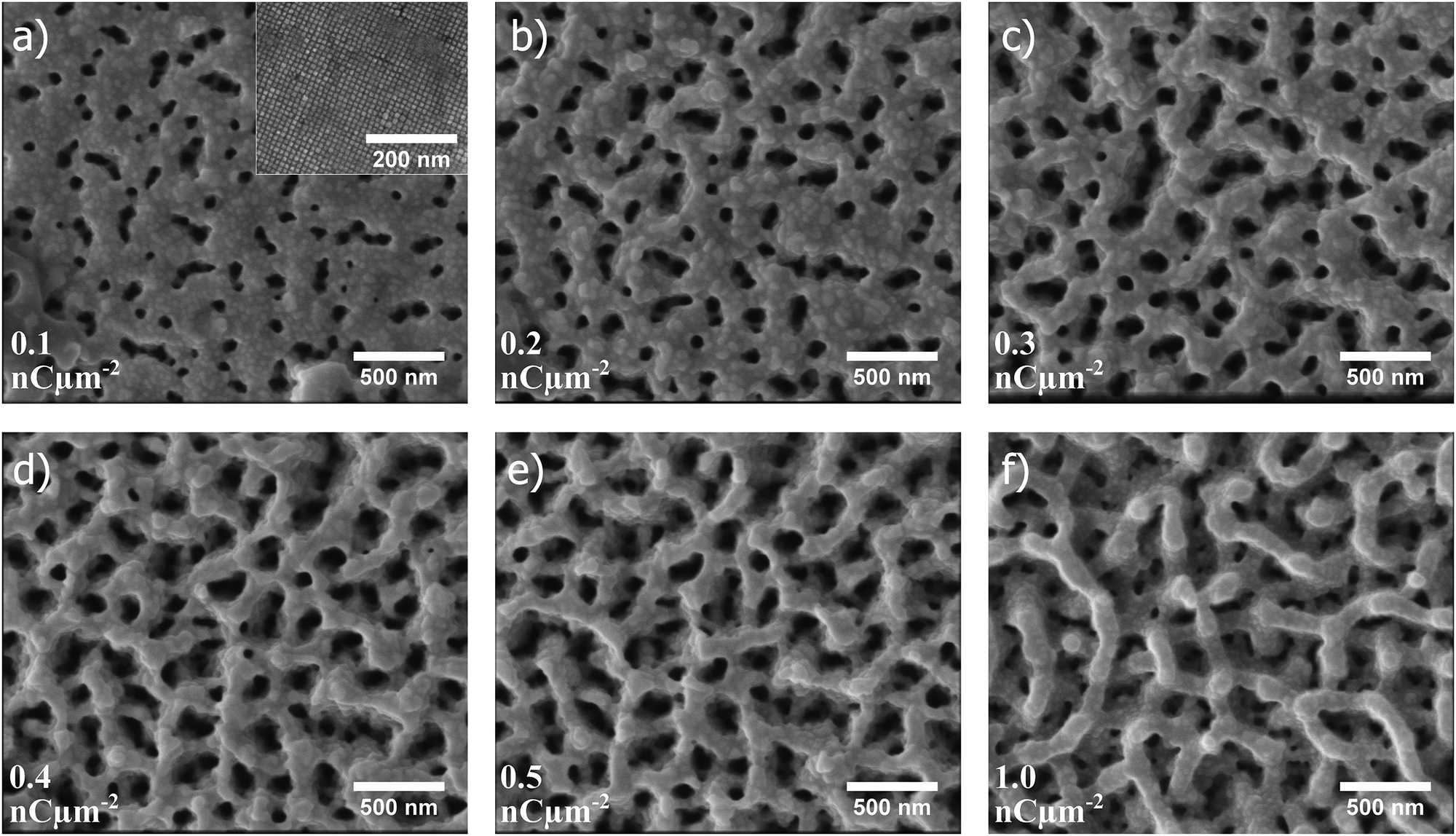 | ||
| Fig. 2 Pore evolution during FIB exposure of a cubic superstructure. The SEM micrographs show the evolution of a porous network as a function of increasing ion beam dose at voltage 30 kV. (a–f) Show the resulting surface after exposure of an ion beam dose of 0.1, 0.2, 0.3, 0.4, 0.5 and 1.0 nC μm−2, respectively. | ||
Interestingly, the superstructures are found to respond differently when exposed to an ion beam voltage below 30 kV. The dependence of pore formation on ion beam voltage is first illustrated for superstructures composed of nanospheres, as shown in Fig. 3 (unexposed surface shown in the inset of Fig. 3a). It is here immediately clear that pore formation can be reproduced when spheres are utilized instead of cubes, which was seen previously in Fig. 2. In Fig. 3a–e, SEM images (all captured at ×100k magnification) depict how the pore size of the resulting structure can be tuned after self-assembly by controlling the acceleration voltage in the FIB milling, in this case set to 2, 5, 10, 20 and 30 kV, respectively (15 and 25 kV shown in Fig. S2, ESI†). The ion beam dose is kept constant at a value of 0.5 nC μm−2 for all applied voltages. Here, the SEM images show a clear trend as to how the pore size distribution is shifted towards smaller values when the voltage is decreased. In the case of 30 kV, a combination of submicron- and nanopores is observed, while at 2 kV solely small nanopores are observed. Measurements of resulting pore sizes at different voltages reveals a linear relationship in the mean pore size versus ion beam voltage (Fig. 3f). The measured pore sizes were fitted to a lognormal distribution, as can be seen for 25 kV in the inset of Fig. 3f, which was used to calculate the statistical mean, standard deviation and mode (i.e. pore size corresponding to distribution maximum) at different ion beam voltages (for more information about distribution fitting at different ion beam voltages, see Fig. S4 and Table S1, ESI†). The standard deviation and mode are also found to increase in a linear manner with increasing ion beam voltage (Fig. S6a and b, ESI†).
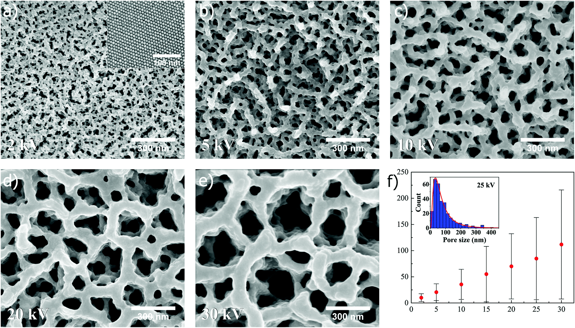 | ||
| Fig. 3 Tuning the porosity of the resulting pore network during ion beam exposure of superstructures composed of nanospheres, by controlling the ion beam voltage at a constant dose of 0.5 nC μm−2. (a–e) Show SEM micrographs of the resulting pore network after ion beam exposure at 2, 5, 10, 20 and 30 kV, respectively. (f) The measured pore sizes were fitted to a lognormal distribution, and mean values were found to increase in a linear manner with increasing ion beam voltage. | ||
When superstructures composed of nanocubes are exposed to FIB at different ion beam voltages, the similar trend as for spheres is revealed, as shown in Fig. 4. In Fig. 4a–e, SEM images (all captured at ×100k magnification) depict how the pore size of the resulting structure is increased when the ion beam voltage is increased from 2 kV to 5, 10, 20 and 30 kV, respectively, at a constant dose of 0.5 nC μm−2 (15 and 25 kV shown in Fig. S3, ESI†). A linear relation is also seen in Fig. 4f where the mean pore size, extracted from lognormal distribution fitting to the measured pore sizes (25 kV in inset), is plotted as a function of ion beam voltage (for more information about distribution fitting at different voltages, see Fig. S5 and Table S1, ESI†). Similarly as for spheres, the standard deviation and mode are for cubes found to increase in a linear manner with increasing ion beam voltage (Fig. S6c and d, ESI†).
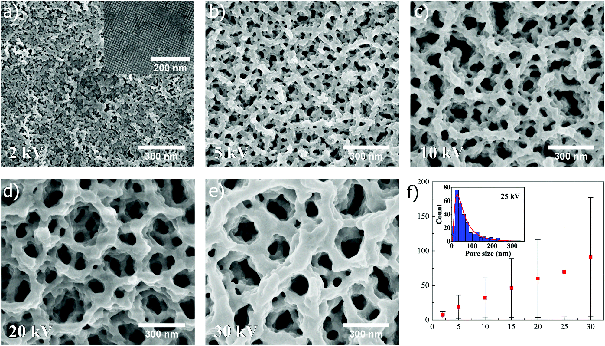 | ||
| Fig. 4 Tuning the porosity of the resulting pore network during ion beam exposure of superstructures composed of nanocubes, by controlling the ion beam voltage at a constant dose of 0.5 nC μm−2. (a–e) Show SEM micrographs of the resulting pore network after ion beam exposure at 2, 5, 10, 20 and 30 kV, respectively. (f) The measured pore sizes were fitted to a lognormal distribution, and mean values were found to increase in a linear manner with increasing ion beam voltage. | ||
Comparing the values in Fig. 3f and 4f, it is clear that the shape of the superstructure constituents (nanoparticle shape) plays an important role in pore formation, as far as mean pore size is concerned (direct comparison in Fig. S7, ESI†). In the case of both spheres and cubes, the mean pore size follows a linear relationship with respect to the applied ion beam voltage, but the mean sizes in case of spheres are, however, generally larger than for cubes. This observation can be understood from a packing factor standpoint, which will always be lower for spheres, considering closed packed structures in both cases. Since there simply exists more space between spherical nanoparticles in a superstructure, compared to cubes, the mean pore size is intuitively observed to be larger. The same holds true for the mode. Interestingly, when the mean pore sizes and modes are plotted as function of ion beam voltage, and subsequently subjected to linear curve fitting followed by extrapolation to zero voltage, the resulting pore sizes for both spheres and cubes are found to be close to the spacing between nanoparticles in the unexposed superstructures, i.e. ∼2–3 nm (Table S2, ESI†), reflecting the intrinsic porosity present in the self-assembled superstructures if the oleic acid matrix is disregarded.
The mechanism for pore formation is attributed to the combination of milling and sintering, i.e. partial melting of the superstructure constituents (nanoparticles) while being exposed to the high energy ion beam. Energy of the ion beam is transferred to the nanoparticle lattice during the collision cascade, as lattice atoms are ejected and amorphization of the lattice happens, which ultimately results in heating.29 Being zero-dimensional nanomaterials isolated from each by an oleic acid matrix, the nanoparticles will not readily dissipate heat generated in the milling process, which thus can promote partial (and even complete) melting and fusion of exposed particles. Moreover, nanoparticles are also known to melt at lower temperatures than their corresponding bulk values, due to a high surface area-to-volume ratio causing instability.30,31 The local temperature during milling depends on several factors, such as thermal conductivity of the material being milled, the geometry, thermal contact to the surrounding environment, and ion beam voltage and current,32 and is thus difficult to accurately predict without extensive modelling. Oleic acid chains are most likely removed in the milling process (Fig. S11, ESI†), causing the nanoparticles to stochastically migrate to nearest neighbours as they are partially milled and melted. This stochastic migration of nanoparticles is presumably dictated by van der Waals interactions between nearest neighbours, in addition to interactions with the high energy Ga+-ions, as the oleic acid matrix is degraded during milling. Hence, as illustrated in Fig. 5a, the nanoparticles merge and form a network of interpenetrating pores (emphasized in the red circle of the inset).
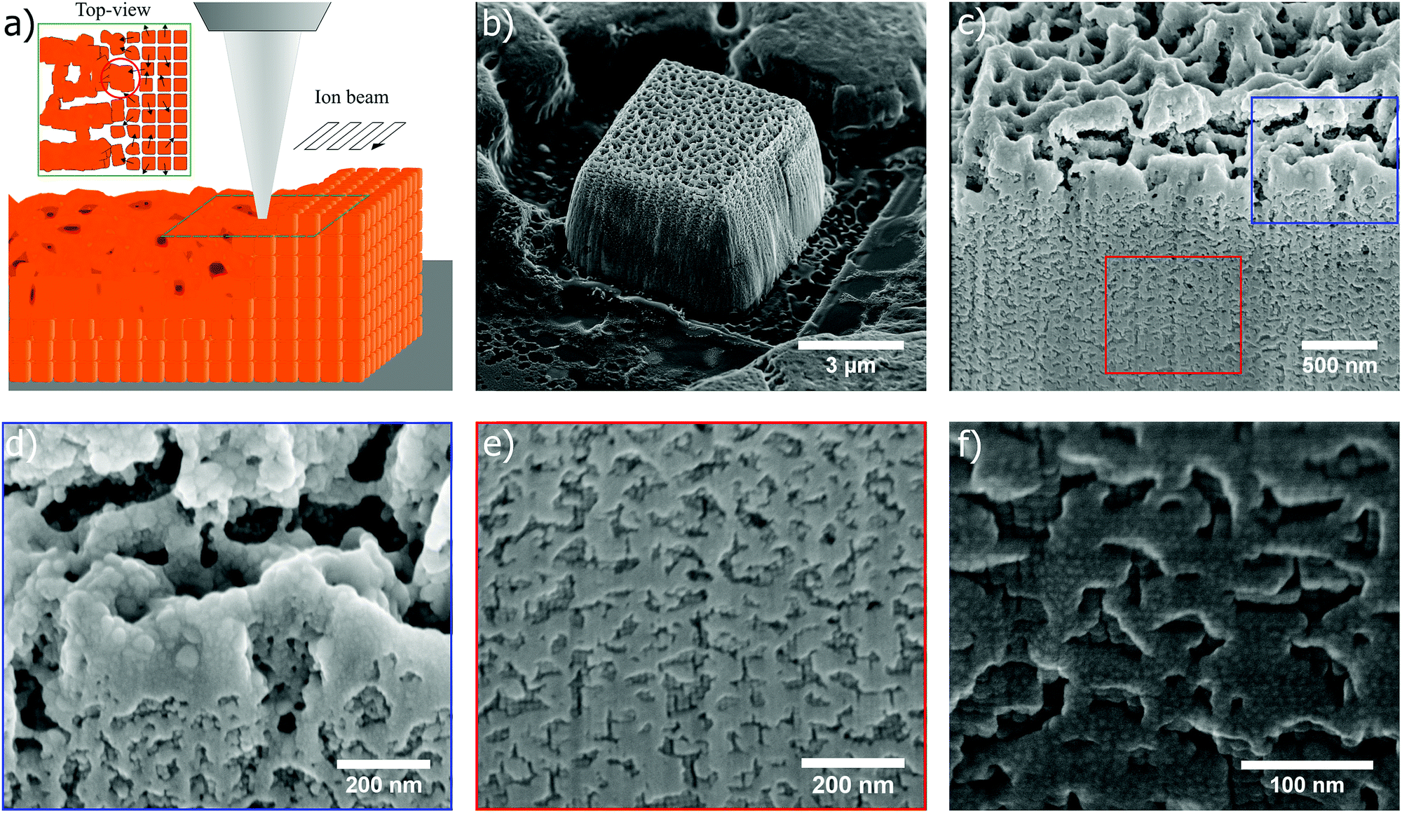 | ||
| Fig. 5 Mechanism for pore formation upon ion beam exposure of a superstructure. (a) As the ion beam is scanned across the surface, milling and local heating cause the nanoparticle constituents to stochastically migrate and merge into nearest neighbours as the oleic acid matrix (not shown) is removed, thus forming a porous network (as emphasized in the red circle of the inset). (b) SEM micrograph of a cubic superstructure exposed to the ion beam at 30 kV with a 0.5 nC μm−2 dose. (c) SEM micrograph showing a milled cross section of an exposed supercubic structure, in which the transition from porous network to crystalline phase can be seen. The blue and red frame are shown as higher resolution SEM images in (d and e), respectively. (d) Interior of the porous network, in which single nanocubes can be seen to have merged together. (e) Cubic stacking of the crystalline phase is shown to become more and more ordered further down in the superstructure. (f) Close-up SEM micrograph of the bottom ordered phase of the structure. The network-like pattern on the surface arises unavoidably as a result of milling and partial melting of cubes near the surface during ion beam exposure of the cross section. | ||
In Fig. 5b, the SEM image shows a tilted view of a cubic superstructure after being exposed to the ion beam at 30 kV with a 0.5 nC μm−2 dose. When a cross section is milled in such a superstructure, the porous network is observed to extend about ∼2 μm into the structure, followed by a smooth transition to the ordered phase, as seen in Fig. 5c (supplementing SEM images in Fig. S8 and S9, ESI†). The blue and red frame in Fig. 5c are shown as higher resolution SEM images in Fig. 5d and e, respectively. The upper part of the exposed structure reveals how individual nanocubes have melted together, and melting is also evident from the shape of the particles which is rendered more spherical in the directly exposed part. A rather rough granular structure can be noticed in the porous framework, especially at the bottom side of the backbone more shielded from the ion beam. The same rough morphology was observed in Fig. 2 in the initial stages of the milling, and was found to become more and more smoothened out after extensive milling (Fig. 2f). The cubic stacking of the crystalline phase is shown in Fig. 5e and becomes more ordered further down in the superstructure (melting of the nanocubes in the crystalline part of the cross section due to interactions with the ion beam during cross section milling is observed to a certain degree, although this is not a part of the original structure). A close-up SEM image of the crystalline part further down in the structure is shown in Fig. 5f. In the unavoidable network-like pattern at the milled cross section, traces of nanoparticles merged together are seen as small brighter dots.
As previously observed from Fig. 3 and 4, lowering the ion beam voltage during superstructure exposure will result in smaller pore sizes. As the voltage is lowered, the milling rate of the nanoparticles will also be lowered, as well as the energy transfer from the ion beam resulting in a decrease in local temperature. This combined lowering of milling rate and local temperature will cause thinner and thinner pore networks to survive the ion exposure, giving rise to both smaller pores and the possibility to tune the pores size. Complete melting of nanoparticles is also less evident at lower voltages, since the pore framework appears to become rougher. At 2 kV, the individual particles comprising the pore network are nearly visible (Fig. 3e and 4e), suggesting again that milling happens to a lower extent and that the local temperature is lowered to the point where only the higher energy surface layers start to melt. At higher voltages, smaller existing pore networks will be milled more readily than thicker ones as time progresses, and redeposition of milled material will occur within the pores, resulting in larger pore networks to grow at the expense of smaller ones (Fig. S8, S10 and Movie S1, ESI†), similar to an Ostwald ripening process.33
In this study, the magnetic oxide cobalt ferrite was chosen as a means of fabricating superstructures exhibiting an ordered lattice. Magnetism played an important role in the actual superstructure fabrication, but is not considered to play an important role in the mechanism of the subsequent pore formation during ion beam exposure. In fact, magnetic properties have been shown to be readily changed during ion beam exposure of magnetic materials, due to lattice amorphization and ion implantation, even to the point where all magnetism is lost.34,35 Energy dispersive X-ray spectroscopy confirmed the significant presence of Ga in as-prepared porous network after ion beam exposure (Fig. S11 and S12, ESI†). Annealing at elevated temperatures could be utilized as a method to repair any potential damage inflicted by the ion beam on the atomic structure of the porous network,36 and possibly further smoothen out the morphology of the backbone. A successful annealing process can potentially form the basis for fabricating porous magnetic materials with tunable porosity. Although not investigated thus far, the atomic structure of the backbone, and how it translates to the surface, is an important aspect in many applications, including catalysis and energy storage. Measures to determine the backbone atomic structure after ion beam exposure, and how it can be modified by annealing, should therefore be taken to further illuminate potential application areas.
All the porous structures in this study were fabricated by means of a focused Ga+-ion beam. The FIB system provides excellent spatial resolution with a typical beam diameter in the order of 10 nm, capable of local exposure with high voltage of an otherwise macroscopic sample. Although this provides excellent control of the location of the fabricated porous structures, i.e. the fabrication of porous materials locally (Fig. S13, ESI†), it would be a very slow process to expose areas up to the order of mm. Broad ion beam exposure, conventionally with Ar+-ions, employs a beam with a typical diameter in the order of 1 mm, and can therefore be utilized as an alternative strategy to expose larger areas in the fraction of the time spent in FIB.37,38 Although materials will probably mill differently when subjected to an Ar+-beam, due to a lower atomic mass than Ga+, there might be less contamination present in the porous backbone after exposure due the inertness of Ar, which can more readily diffuse out of the lattice at elevated temperatures. An interesting question which should be addressed, is how a superstructure would respond to exposure of focused and broad ion beams of different species (other than Ga+), with different mass and level of inertness, like He+, O+, Ar+ and Xe+. This could potentially offer further novel fabrication alternatives in the route for designing 3D nanoporous materials.
The mechanism for porous network formation during ion exposure of the magnetic superstructures in this study, is not considered to be dependent on magnetism. This suggests that any non-magnetic inorganic materials could take the place of cobalt ferrite in this fabrication process, which is also the subject of further investigation. Non-magnetic nanoparticles will not accommodate directional superstructure growth (such as supercubic structures), thus making it easier to evenly coat the entire substrate. Moreover, the opportunity to choose the porous backbone material in the fabrication would make this novel strategy very appealing in a wide range of applications. This strategy could also be extended to develop multimetallic porous materials from a single solid superstructure made from nanoparticles of different materials. Furthermore, experiments will be conducted to elucidate the importance of ordering, packing and size of the nanoparticles in the superstructures, with respect to pore formation upon ion beam exposure. A disordered superstructure would be easier to fabricate than an ordered one, and will most likely be rendered porous upon ion beam exposure, although an associated smaller packing factor will presumably have and influence on the resulting pores size distribution (the significance of packing on the basis of nanoparticle shape was established above, where a smaller packing factor was found to increase the pore sizes). The nanoparticle size is also an important aspect since melting is dictated by size. There will most likely exist a critical size above which milling predominantly occurs over melting with no merging of particles into a porous network.
Conclusions
In summary, a combination of nanoparticle self-assembly (bottom-up) and FIB milling (top-down), has been demonstrated to fabricate porous structures with tunable pore size distribution from the nanoscale to the submicron-scale. Both nanosphere- and nanocube-based superstructures of cobalt ferrite were found to yield porous structures upon ion beam exposure, with the possibility to tune the pore size distribution towards smaller values by reducing the ion beam voltage. The mean pore size was in both cases found to increase linearly with respect to ion beam voltage. Sphere-based superstructures generally yielded larger pore sizes than cube-based, due to a less closer packed structure prior to ion beam milling, illustrating how the shape of superstructure constituents contributes to tuning the resulting porosity. Combined milling and partial melting of nanoparticles during ion beam exposure was established as the mechanism for pore formation. A superstructure composed of nanoparticles is considered critical as a starting point prior to ion beam exposure, as the spacing between each nanoparticle give rise to stochastic migration and merging into a porous network during exposure. This discovery is believed to open up new possibilities in many research fields, where the control of local patterns or large scale porous structures, with the possibility to choose backbone material, is highly desired, such as tissue engineering, drug delivery, microfluidics, catalysis, separation, energy storage and conversion, sensing devices, as well as anti-icing applications.Experimental
Experimental methods are available in the ESI.†Conflicts of interest
There are no conflicts to declare.Acknowledgements
The Research Council of Norway is acknowledged for the support to the Norwegian Micro- and Nano-Fabrication Facility, NorFab, project number 245963/F50. Our colleague Aleksander B. Mosberg is acknowledged for fruitful discussions regarding FIB operations. We acknowledge support from the Research Council of Norway through the Norwegian Center for Transmission Electron Microscopy, NORTEM (197405/F50).References
- T. Wang, X. Wang, D. LaMontagne, Z. Wang, Z. Wang and Y. C. Cao, J. Am. Chem. Soc., 2012, 134, 18225 CrossRef CAS PubMed.
- L. Wu, J. J. Willis, I. S. McKay, B. T. Diroll, J. Qin, M. Cargnello and C. J. Tassone, Nature, 2017, 548, 197 CrossRef CAS PubMed.
- X. Bouju, E. Duguet, F. Gauffre, C. R. Henry, M. L. Kahn, P. Melinon and S. Ravaine, Adv. Mater., 2018, 30, 1706558 CrossRef PubMed.
- J. J. Urban, D. V. Talapin, E. V. Shevchenko, C. R. Kagan and C. B. Murray, Nat. Mater., 2007, 6, 115 CrossRef CAS PubMed.
- K. J. Bishop, C. E. Wilmer, S. Soh and B. A. Grzybowski, Small, 2009, 5, 1600 CrossRef CAS PubMed.
- L.-Y. Chen, J.-S. Yu, T. Fujita and M.-W. Chen, Adv. Funct. Mater., 2009, 19, 1221 CrossRef CAS.
- M. Hakamada and M. Mabuchi, J. Alloys Compd., 2009, 485, 583 CrossRef CAS.
- T. Wada, K. Yubuta, A. Inoue and H. Kato, Mater. Lett., 2011, 65, 1076 CrossRef CAS.
- I. McCue, E. Benn, B. Gaskey and J. Erlebacher, Annu. Rev. Mater. Res., 2016, 46, 263 CrossRef CAS.
- C. Li, O. Dag, T. D. Dao, T. Nagao, Y. Sakamoto, T. Kimura, O. Terasaki and Y. Yamauchi, Nat. Commun., 2015, 6, 6608 CrossRef CAS PubMed.
- V. Malgras, H. Ataee-Esfahani, H. Wang, B. Jiang, C. Li, K. C. Wu, J. H. Kim and Y. Yamauchi, Adv. Mater., 2016, 28, 993 CrossRef CAS PubMed.
- C. Zhou, T. Segal-Peretz, M. E. Oruc, H. S. Suh, G. Wu and P. F. Nealey, Adv. Funct. Mater., 2017, 27, 1701756 CrossRef.
- E. A. Anumol, A. Halder, C. Nethravathi, B. Viswanath and N. Ravishankar, J. Mater. Chem., 2011, 21, 8721 RSC.
- S. Das, P. Ranjan, P. S. Maiti, G. Singh, G. Leitus and R. Klajn, Adv. Mater., 2013, 25, 422 CrossRef CAS PubMed.
- G. Singh, H. Chan, A. Baskin, E. Gelman, N. Repnin, P. Král and R. Klajn, Science, 2014, 345, 1149 CrossRef CAS PubMed.
- L. H. Qian, X. Q. Yan, T. Fujita, A. Inoue and M.-W. Chen, Appl. Phys. Lett., 2007, 90, 153120 CrossRef.
- A. Wittstock, V. Zielasek, J. Biener, C. M. Friend and M. Bäumer, Science, 2010, 327, 319 CrossRef CAS PubMed.
- M. M. Biener, J. Biener, A. Wichmann, A. Wittstock, T. F. Baumann, M. Baumer and A. V. Hamza, Nano Lett., 2011, 11, 3085 CrossRef CAS PubMed.
- W. Wang, H. Tao, Y. Zhao, X. Sun, J. Tang, C. Selomulya, J. Tang, T. Chen, Y. Wang, M. Shu, L. Wei, G. Yi, J. Zhou, L. Wei, C. Wang and B. Kong, Theranostics, 2017, 7, 1966 CrossRef PubMed.
- G. Turnbull, J. Clarke, F. Picard, P. Riches, L. Jia, F. Han, B. Li and W. Shu, Bioact. Mater., 2018, 3, 278 CrossRef PubMed.
- G. A. Seisenbaeva, M. P. Moloney, R. Tekoriute, A. Hardy-Dessources, J. M. Nedelec, Y. K. Gun'ko and V. G. Kessler, Langmuir, 2010, 26, 9809 CrossRef CAS PubMed.
- R. Knob, V. Sahore, M. Sonker and A. T. Woolley, Biomicrofluidics, 2016, 10, 032901 CrossRef PubMed.
- G. Sneddon, A. Greenaway and H. H. P. Yiu, Adv. Energy Mater., 2014, 4, 1301873 CrossRef.
- M. H. Sun, S. Z. Huang, L. H. Chen, Y. Li, X. Y. Yang, Z. Y. Yuan and B. L. Su, Chem. Soc. Rev., 2016, 45, 3479 RSC.
- K. Liang, L. Li and Y. Yang, ACS Energy Lett., 2017, 2, 373 CrossRef CAS.
- P. W. Wilson, W. Lu, H. Xu, P. Kim, M. J. Kreder, J. Alvarenga and J. Aizenberg, Phys. Chem. Chem. Phys., 2013, 15, 581 RSC.
- P. Juuti, J. Haapanen, C. Stenroos, H. Niemelä-Anttonen, J. Harra, H. Koivuluoto, H. Teisala, J. Lahti, M. Tuominen, J. Kuusipalo, P. Vuoristo and J. M. Mäkelä, Appl. Phys. Lett., 2017, 110, 161603 CrossRef.
- N. Bao, L. Shen, P. Padhan and A. Gupta, Appl. Phys. Lett., 2008, 92, 173101 CrossRef.
- C. A. Volkert and A. M. Minor, MRS Bull., 2007, 32, 389 CrossRef CAS.
- K. K. Nanda, Pramana, 2009, 72, 617 CrossRef CAS.
- J. Zhu, Q. Fu, Y. Xue and Z. Cui, Mater. Chem. Phys., 2017, 192, 22 CrossRef CAS.
- T. Ishitani and H. Kaga, J. Electron Microsc., 1995, 44, 331 CAS.
- P. W. Voorhees, J. Stat. Phys., 1985, 38, 231 CrossRef.
- C.-M. Park, J. A. Bain, T. W. Clinton and P. A. A. van der Heijden, J. Appl. Phys., 2003, 93, 6459 CrossRef CAS.
- J. Fassbender and J. McCord, J. Magn. Magn. Mater., 2008, 320, 579 CrossRef CAS.
- A. Schilling, T. Adams, R. M. Bowman and J. M. Gregg, Nanotechnology, 2007, 18, 035301 CrossRef CAS PubMed.
- R. M. Langford and A. K. Petford-Long, J. Vac. Sci. Technol., A, 2001, 19, 982 CrossRef CAS.
- Z. Huang, J. Microsc., 2004, 215, 219 CrossRef CAS PubMed.
Footnote |
| † Electronic supplementary information (ESI) available: Experimental methods; supplementing SEM micrographs; EDX analysis; statistical analysis including plots and tables; movie showing live pore evolution. See DOI: 10.1039/c8mh01112e |
| This journal is © The Royal Society of Chemistry 2018 |