
 Open Access Article
 This Open Access Article is licensed under a Creative Commons Attribution-Non Commercial 3.0 Unported Licence
Materials chemistry approaches to the control of the optical features of perovskite solar cells
Mauricio E.
Calvo
 *
*
Institute of Materials Science of Seville, Spanish National Research Council, University of Seville, Calle Américo Vespucio 49, 41092, Seville, Spain, Email: mauricio.calvo@icmse.csic.es
First published on 22nd September 2017
Abstract
Perovskite solar cells have revolutionized the field of photovoltaics. Apart from their impressive photo-conversion efficiencies, the ease of their fabrication – principally when carried out by solution processing – has permitted addition of new functionalities to the photovoltaic cell. Some of these features are related to the optical properties. In this review, the different materials chemistry approaches that allow controlling the spectral absorption of ABX3 perovskite layers and the changes that they produce in the visual aspect of the solar cell will be covered. These modifications can be done either by playing with the composition of the precursors or by integrating different types of nanostructures. Spectral bandgap tuning, semitransparency, color and enhancement of light absorption are examples of how these modifications operate in the core of ABX3 perovskite solar cells. These optical features bring benefits in terms of photo-conversion efficiencies or else in the aesthetical integration of perovskite solar cells with architectonic elements for building integrated photovoltaics. Additionally, surface passivation approaches are covered to show its effect over the photo-conversion efficiency and stability of the cell.
 Mauricio E. Calvo | Dr M. E. Calvo is Doctor in Chemistry from the University of Buenos Aires, Argentina. He is a happy father of four kids and is a member of the permanent staff of the Spanish National Research Council (CSIC). He is part of the Multifunctional Optical Materials Group at the Institute of Materials Science of Seville where he has been working for ten years. Nowadays, his main research interest is focused on the solution process of optical porous hybrid nanostructured materials for different applications like solar protection, optoelectronic devices and sensors. He is the author of more than 50 publications and 7 patents and he is/was the supervisor for several PhD theses. More information at http://mom.icmse.csic.es/group-members/mauricio-calvo/. |
1. Introduction
The global energy demand is increasing year by year due to the growing population and the changes in the lifestyle of societies around the entire world.1 The ancient practice of burning off carbon based compounds to generate energy has inflicted very serious collateral issues such as global warming and environmental pollution.2 Hence, the urgent requirement to move to cleaner energy sources has mobilized a huge research effort on renewable energies.3 In this scenario, solar radiation appears as an unlimited source of energy capable of supplying the global demand if only 1% of the irradiation is harvested.4 It has been proposed that at least 25% of the worldwide energy demand could be met by solar-driven energy in the next decades through different exploitation technologies.5 Nowadays, photovoltaic solar cell technology based on silicon has been demonstrated to be a mature technology that transcends many research fields. However, lower cost per kilowatt and facile fabrication is still required for widespread application. In this context, solar cells based on the ABX3 perovskite family have irrupted in the photovoltaics scene generating a revolution in the field.6 Over the last five years, continuous research in the subject has served to proliferate, expand and unite different areas of material sciences. This extraordinary effervescence drove the photon conversion efficiencies of perovskite solar cells (PSCs) from 6.55% in 2009 (ref. 7) to 22.1% in 2016.8 This impressive growth accounts for the ubiquitous activity related to the ABX3 perovskite field, which has achieved – in terms of photo-conversion efficiency – in only five years the same change that has required 20 years in silicon based photovoltaics. This sets ABX3 PSCs as a promising candidate that could bring energy cost down to 4.5 centi€ per kW h.9ABX3 perovskite compounds are inorganic or hybrid organic–inorganic metal halide crystalline solids where B is a metal (principally Pb or Sn), X is a halide (I, Br or Cl) and A is a monovalent cation that can be inorganic (cesium) or organic (alkylammonium or alkylamidinium). From the point of view of the opto-electronic properties, ABX3 perovskites are considered mostly as direct band gap semiconductors with strong absorption in the visible region. Furthermore, illumination generates labile excitons that fade into charge carriers with balanced effective masses, high mobilities and long diffusion lengths.10 These characteristics also make the ABX3 perovskite family suitable candidates for application in fields like photon or electron induced light emission,11 lasing,12 photodetection,13 catalysis14 and sensing.15
This family of compounds also presents significant advantages in terms of synthesis because it can be prepared easily as thin films from low-cost and earth abundant precursors. In addition, ABX3 perovskites can be prepared by different wet chemistry based methods.16–18 Perovskite precursors are dissolved in suitable solvents and then deposited by spin or dip coating in a process that can be completed in one or in two steps. With low environmental impact and thermodynamic cost, wet deposition methods permit19,20 mass production by high-throughput solution processes like inkjet printing,21 brush painting22 or slot-die coupled to a roll-to-roll printing process.23,24 Furthermore, ABX3 perovskite surfaces can be passivated easily with the aim of achieving stability of the PSC against the environment.25
As it occurs with classical photovoltaic semiconductor devices, ABX3 perovskite solar cells generate a photo-voltage once light impinges on a thin film (thickness 200–400 nm) placed between two contacts and electrically connected to them by selective charge carrier layers. This energy conversion system consists basically in two processes: (i) the absorption of luminous energy (photons) to produce electrons (e−) and holes (h+) and (ii) the production of electrical energy through the collection and driving of such carriers, which give rise to the appearance of current and voltage. Both processes are tremendously efficient in this perovskite family since the structure harvests visible light very efficiently and supports both long carrier lifetimes, typically in the microsecond range, and highly efficient charge separation.26 The aforementioned features make ABX3 perovskite solar cells present high open circuit voltages and large photocurrents, both very close to the thermodynamic limit.27,28
At present, many efforts are oriented to the study of the interaction of the cell with the impinging light. The elucidation of charge carrier migration and recombination processes, and the study of cell stability and its working principles, are subjects of high interest nowadays. The active material of this solar cell type is an ABX3 perovskite layer where photons impinging on the cell, in analogy with a chemical reaction, are the only feeders of the luminous-to-electric conversion and they are consumed during the light absorption process. This has generated increasing interest in the search for more efficient ways to improve light trapping in the active layer of the cell29 and in the comprehension of the photo-physical processes that are unleashed there.30,31 It has been largely demonstrated that a wide palette of nanostructures is able to manage photons in the range of optical frequencies where a solar cell operates (ideally 350 nm < λ < 2500 nm).32,33
Furthermore, photons impinge on our retinae after crossing the pupils. This sensorial change is processed by our brains giving us color sensation. It is well-known that colors modify our perception and influence our state of mind. Color can be quantitatively linked to the interaction of the optical properties with the electromagnetic radiation through color spaces (i.e. CIE 1931). This sensorial response induces the expansion of ABX3 PSCs in the field of building integrated photovoltaics (BIPV) by combining their impressive efficiencies with aesthetical and ornamental features, such as semitransparency, color or texture.34 All these features make ABX3 perovskites an interesting material for the optical control inside the cell.
In this review I will cover the recent advances in materials chemistry methods that allow modification, and fine tuning, of the spectral response of ABX3 perovskites. First, I will focus on a brief description of the optical constants of ABX3 layers. Next, I analyze how the composition of ABX3 affects its optical properties. Next, I describe the efforts made to modify these features by integrating different types of nanostructures that provide PSCs with color, semitransparency or both.35 Finally, I show the efforts recently made on ABX3 surface passivation. Both types of modifications have an impact over the efficiencies but can provide an added value in terms of the device functionality and stability.
2. Optical properties of ABX3 perovskites
As it generally occurs in semiconductors, the optical properties of ABX3 perovskites are intimately related to the crystalline structure. Briefly, the structure of the perovskite family can be defined by a cubic structure in which a metallic (M2+) center is coordinated by the halide (X−) in an octahedral configuration ([MX6]4−). The octahedra share corners with their neighbors and cations (A+) counterbalance the charge occupying the 12-fold cavity formed by eight of the mentioned octahedra. This octahedral arrangement could present distortion with a reduced symmetry (pseudocubic or tetragonal lattice) that affects the electrical, optical and magnetic properties of PSCs.36ABX3 perovskites have been the subject of study since the beginning of the 90s.37 The use of ABX3 perovskites in solar cells was pioneered by Miyasaka and co-workers in 2009,7 and improved by Park et al. in 2011.38 In these early studies, the photovoltaic cell was constructed following the configuration of a dye sensitized solar cell (DSC): a photoanode of mesoporous TiO2 with thickness between 5.5 and 12 μm is impregnated with methyl ammonium lead iodide (CH3NH3PbI3, MAPI) or methyl ammonium lead bromide, (CH3NH3PbBr3MAPBr). These compounds sensitized the TiO2 scaffold, absorbing light in the visible region and injecting electrons in the TiO2 conduction band. The optical properties of this architecture can be described in a first approximation by the effective medium theory, considering a nanoporous TiO2 layer filled almost totally with electrolyte solution and an absorbing material all of them characterized by a complex refractive index and a fill factor.39
However, the advent of more efficient PSC configurations in which MAPI (or any ABX3 compound) is in the form of a thin film aroused great interest in the description of its optical properties, as they turned out to be extremely dependent on the method of preparation employed.40,41 In these highly efficient architectures, a perovskite layer with 300–400 nm thickness is sandwiched between a hole transporting layer (spiro-OMeTAD, PTAA, CuSCN, etc.) and an electron transporting layer (TiO2, Nb2O5, SnO2, etc.). In addition, a thin layer of a porous metal oxide scaffold is deposited between the ETL and the ABX3 perovskite layer. Finally, FTO and gold contacts are attached to the ETL and HTL, respectively, to close the circuit. The rational design of any type of photovoltaic devices requires the optical constants of each layer that are part of the device. The optical modelling of this thin layer configuration needs the estimation of the complex dielectric permittivity of the ABX3 perovskite as well as of the other components of the solar cell.
The complex refractive index, N, is defined in eqn (1):
| N = n − ik | (1) |
 | (2) |
| ε1 = n2 − k2 | (3) |
| ε2 = 2nk | (4) |
| ε = ε1 − iε2 | (5) |
It is important to mention that both real and imaginary parts of the refractive index are dependent on the wavelength and connected to each other through the Kramers–Kronig relationships. This allows calculation of ε1 from ε2 and vice versa.
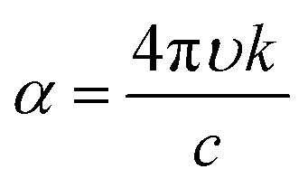
The set of parameters (n, k) of thin layers is usually determined by the variable angle spectroscopic ellipsometry (VASE) technique,47 or by optical spectroscopy in the ultraviolet-visible-near infrared region of the spectrum.48 The first technique detects changes in the polarization of the transmitted or reflected light that impinges over a thin layer. The second method requires the spectral measurement of reflectance (R) and/or transmittance (T). Both mentioned techniques have been largely applied with consistent results in the ABX3 perovskite field.43,44,49–51 Collected measurements were used to describe a model that can be fitted with an appropriate dispersion relationship formula. The most often used models to extract n and k values are based on the Cauchy equations, Sellmeier relationship, Lorentz oscillator model and Forouhi–Bloomer relationship among others. In particular, the ABX3 perovskite family adopts the Forouhi–Bloomer (FB) multiple oscillator dispersion relationship since it takes into account the crystalline character of MAPI films and is Kramers–Kronig consistent. Once the values of n and k are extracted, they are used to fit experimental R and T through an analytical method that transforms the optical constants described above and the thickness of the film in that spectral quantities.39 Nevertheless, the FB dispersion model requires the measurement of almost three different R and T spectra since the number of fitting parameters increases. These spectra can be obtained from samples with different thicknesses or from the same sample at different light-incident angles. It is important to notice that the accurate determination of the optical parameters demands the fabrication of homogeneous ABX3 thin films with uniform thickness and plane parallel interfaces since spectrophotometric techniques, especially VASE, are sensitive to surface roughness.52 Both requirements are not always achievable by solution process preparation.53 An overview of the related literature shows that perovskite layers obtained by wet deposition methods present ABX3 nanocrystals with grain sizes in the range of 50–200 nm and surface roughness around 10–20 nm.18,43 To solve this issue, the ABX3 perovskite film is modelled as a double layer composed of a bulk component and a rough component. The former presents homogeneous properties whereas the other layer considers an effective medium approach composed approximately of 50% air and 50% ABX3 perovskite. This mixed optical response can be represented by means of the Bruggeman equation. In the last few years, efforts to improve these features have given rise to smoother surfaces with roughness on the order of 2 nm, which is achieved by a careful control of the reaction kinetics.54,55Fig. 1 shows the extracted n and k values for MAPI layers prepared by different synthesis methods. The wide range of values obtained is remarkable.56 In view of this, exhaustive optical characterization of any ABX3 perovskite synthesized by a new method seems mandatory if a full understanding of the response of a device integrating it is desired. An estimation of the roughness of an ABX3 perovskite layer by atomic force microscopy will be helpful during modelling of the optical properties.
 | ||
| Fig. 1 Real part of the refractive index (n, continuous line) and extinction coefficients (k, dashed lines) of MAPI perovskite layers prepared employing different techniques. Data were adapted from the following references: black;42 orange;43 blue;44 brown;45 red.46 | ||
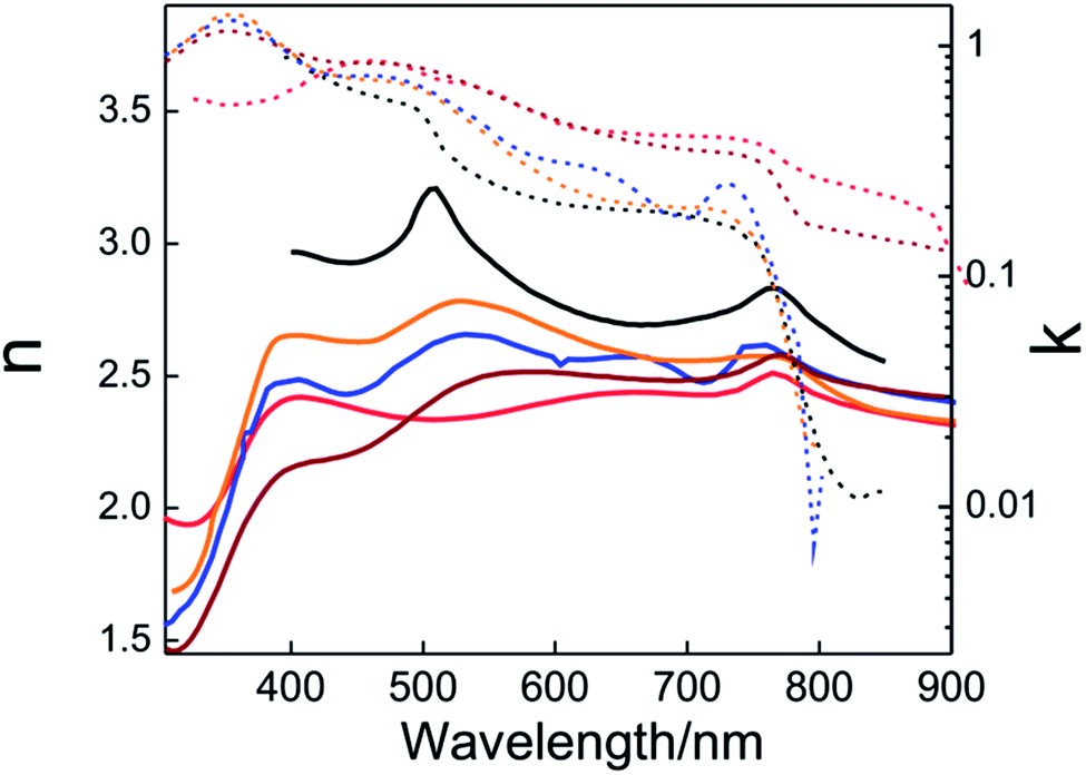
Once the dielectric permittivity of each component in the solar cell is determined, it is possible to model its optical behavior. The easiest way to calculate the optical response of a PSC is to consider it as a multilayered structure composed (in general) of glass substrate/FTO/ETL/(opt.) infiltrated scaffold/PVK/HTL/metal layer. A theoretical method based on the transfer matrix formalism, successfully used in the past with other types of layered cells,39,57–59 is the most extended way to model the optical response of PSCs. The method allows calculation of the transmission, reflection and absorption in each layer or layer interface. The inputs of this model are the thicknesses and the optical constants of the constituting layers. It is important to remark that the optical properties of the layers must be isotropic and homogeneous (i.e. the refractive index does not depend on the thickness of the layer). The condition of parallel-plane interface can be solved in a similar way to that described above with non-planar perovskite layers. The rough interfaces can be modelled according to the effective medium approximation. This approach also has to be considered if perovskite infiltrates the porous scaffold used in the cell. The transfer matrix method allows calculation of the spatial and the spectral distribution of the electric field across the whole cell as depicted in Fig. 2a. This calculation delivers useful information such as the fraction of the light absorbed in each component of the solar cell, providing insight into productive (which could generate photocurrent) and parasitic absorption. Often the optical models can be combined with charge transport models to provide the extracted current density from the device.58 Interestingly, this allows us to change any layer of the PSC to either minimize reflections or localize the electromagnetic field intensity in the ABX3 perovskite absorbing layer to optimize the efficiency of the system. As an example, in Fig. 2b, the theoretical estimation of the photocurrent density is plotted versus the thickness of the perovskite layer.
 | ||
| Fig. 2 (a) Theoretical calculation of the spatial (0.0–1.6 μm) and spectral (400–800 nm) distribution of the electric field inside a PSC that is built using the following architecture: FTO/TiO2 layer/porous scaffold filled with perovskite/perovskite overlayer/spiro-OMeTAD/gold. Dashed white lines represent the interfaces between the mentioned layers. (b) Theoretical calculation of the short circuit photocurrent density produced by a planar PSC with different MAPI thicknesses of (A) 145 nm, (B) 275 and (C) 435 nm. (c) External quantum efficiency (black solid line) determined experimentally and internal quantum efficiency (orange dashed line) obtained from the calculation of the fraction of light absorbed by the perovskite material. (a) and (c) Reprinted with permission from ref. 50 (a), (c) Copyright 2015 American Chemical Society. (b) From ref. 44 Copyright 2015 Royal Society of Chemistry. | ||
Local maxima appear in the curve showing the mentioned thin film interference effects on the photo-generated current. Sometimes, the development of a charge transport model is not an easy task. However, the theoretical model also allows estimating the internal quantum efficiency (IQE) from experimental measurements of external quantum efficiency (EQE), as this is the ratio between the measured EQE and the calculated absorptance (A) of the perovskite layer,42,50 as shown in Fig. 2c. Discrepancies between IQE and A curves or IQE values significantly lower than one (IQE ≪ 1) probe that there are some issues in the charge transport. On the other hand, strong spectral variations of the IQE can be related to a sort of optical problem in the cell. The model can also provide the photon absorption profiles that serve as an input to the aforementioned charge transport models.
3. Controlling the absorption spectrum by chemical modification
The extinction coefficient spectrum resembles the optical absorption profile of the compound. In the plots presented above in Fig. 1 it can be seen that most of these samples present a sharp absorption edge at λ ≅ 800 nm. At higher energies (lower wavelengths), the larger values of the extinction coefficient give rise to even stronger photon absorption. This feature makes a 300 nm thickness layer of MAPI present a dark brownish color. However, as we mentioned in the introduction of this manuscript, a potential integration of PSC in architectonic elements needs the development of more aesthetically versatile structures. The look of a cell will be determined by the convolution of the source (typically the sun, but not necessarily) radiation spectrum, the solar cell reflectance and the photopic response of the human eye. The initial approach to control the aesthetics of ABX3 solar cells consisted in the substitution of the elements of the VII group, the replacement of the cation B or the changing of A cation. These substitutions have direct or indirect effects on the bandgap energy and they are described in the next section. Despite the numerous reviews that can be found in the literature related to this subject, in this work, the composition analysis is provided only to give to the reader the comprehensive elements that work as tools to understand how the Ebg tunability affects not only the aesthetics of the cells but also the functionalities described in the next sections.3.1 Tuning the band gap
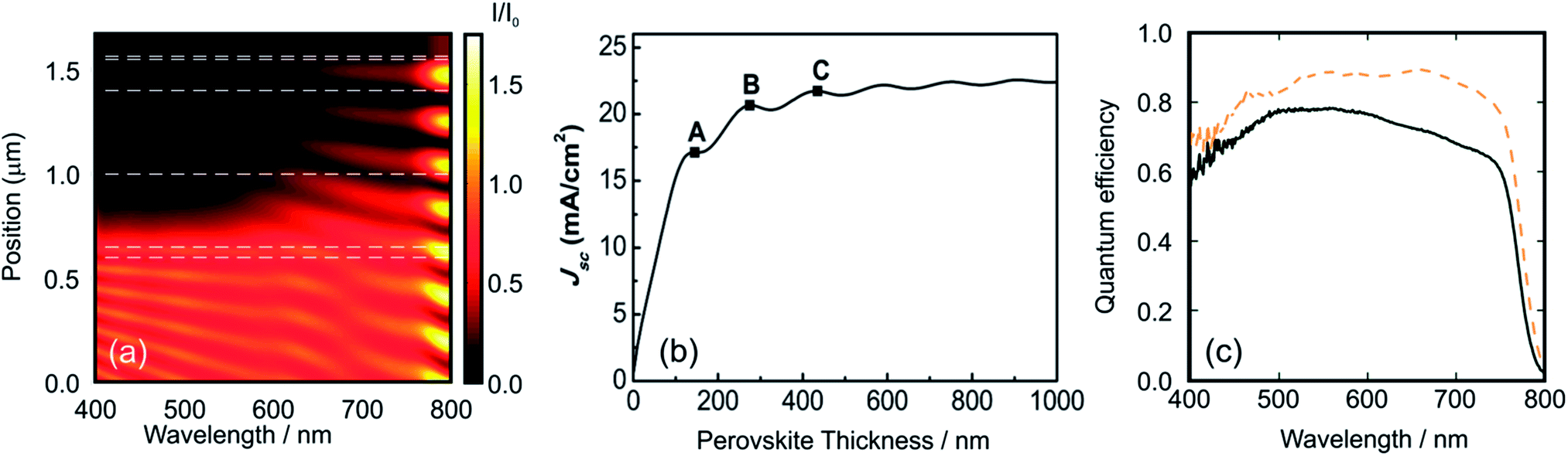
Fig. 3a discloses the lattice parameters as well as the band gap energies for a series of MAPbX3 perovskites where X is a combination of I/Br or Br/Cl. It can be noticed that the increase in the Ebg is correlated with the decrease in the cell parameter length produced by smaller anion incorporation.
 | ||
| Fig. 3 (a) Lattice parameter (green squares) and Ebg (violet squares) for a methylammonium lead halide layer series with the formulae MAPb(BrxCl(1−x))3 and MAPb(I(1−x)Brx) (chloride, right data and iodide, left data from the center of the figure). (b) Absorption spectra obtained from MAPb(I(1−x)Brx)3 layers with x = 0 (black line), x = 0.33 (orange line), x = 0.66 (green line) and x = 1 (violet line). (c) Pictures obtained from the perovskite layer deposited on TiO2 over FTO glass with the composition MAPb(I(1−x)Brx)3, the value of x is indicated in the image. (d) Photocurrent density vs. voltage curves obtained using a series of PSCs with the composition MAPb(I(1−x)Brx)3, where x = 0 (black line), x = 0.13 (orange line), x = 0.2 (green line), x = 0.29 (blue line), x = 1.0 (violet line). (e) Incident photon to charge carrier efficiency photocurrent acquired for the MAPb(I(1−x)Brx)3 series, line colors follow the same pattern of (b). Data were extracted from ref. 48 (a), (d), ref. 47 (a) and ref. 63 (b) and (d). Image reprinted with permission from ref. 48. (c) Copyright 2014 American Chemical Society. | ||
The small change in the slope in the represented magnitudes (lattice constant and Ebg) could be associated with a crystalline phase change of the ABX3 perovskite as halide substitution takes place. Fig. 3b shows the optical absorption profile obtained for four ABX3 perovskites with different compositions. In this case, the content of bromide is replaced gradually by iodide causing a shift to larger wavelengths. The ratio I/Br or Br/Cl in the ABX3 perovskite layer can be modified experimentally by changing the molar ratio of the precursors in the starting solutions. Methyl ammonium halides and lead halides can be dissolved together to achieve the desired composition as the starting point to deposit in one step an ABX3 perovskite film. Seok et al. pioneered the tuning of PSC color by changing gradually the I/Br ratio in the liquid precursor solutions and next depositing them by spin coating.62 It was also demonstrated that the lattice parameter of the tetragonal or cubic MAP[BrxI(1−x)]3 increases as the bromide content diminishes and, more interestingly, it is probed that this ratio is very similar to the composition of the liquid precursors. Further EDS experiments63 or ion chromatography64 confirms that the compositions of the deposited layers of mixed-halide ABX3 perovskites are related closely to the stoichiometry of the precursors.
Fig. 3c shows a series of photovoltaic devices in which the perovskite layer was prepared by spin coating precursors with different Br/I ratios. Other preparation methods such as dip coating sequential deposition can also be used. In this case, the immersion time or the concentration of the precursors in the wetting solution is varied in order to obtain the desired MAPb[BrxI(1−x)]3 compound. In these Br–I mixed perovskite systems, (whichever method is used) the color palette cannot be extended beyond yellowish orange due to the limit value of the Ebg of MAPbBr perovskite (λ ≅ 530 nm). As it was expected, an increment in the bromide content of the precursor produces an increase in the open circuit voltage (Voc) and a reduction in the short circuit photocurrent of the solar cell. This is due to the large Ebg of MAPbBr (compared with MAPI) which leads to a diminution of the fraction of the light absorbed by the PSC with consequent increase of the electrochemical potential of the photo-generated electrons in the conduction band. This effect is nicely disclosed in Fig. 3d where a series of I/V curves obtained for different MAPb[BrxI(1−x)]3 compositions are represented. The measured IPCE curves confirm the modification of the band gap edge as the composition of the halide is varied (Fig. 3e). However, mixed Br–I perovskite layers present light induced phase segregation that causes limitations in the Voc of the cell. The partial replacement of methyl ammonium by cesium or formamidinium improves the stability of the perovskite layer. In these cases, it is possible to stabilize the solar cell at all Br–I compositions.64,65 Recent advances in this direction have demonstrated that the perovskite layer that contains a ternary mix of A cations seems to be the optimal composition in terms of time-stable photo-conversion efficiency.66
In order to expand the color palette of PSCs, it is necessary to move to the Br–Cl mixed perovskite systems which can cover the greenish-blue and the blue region of the electromagnetic spectrum.61 However, mixed Br–Cl perovskite systems do not present a real interest in photovoltaic conversion due to their wide Ebg (Fig. 3a) that prevents harvesting of photons in the high-efficient solar irradiation wavelengths. Nevertheless, these systems are suitable for light emission applications.
The synthesis of the MASnI3 perovskite family was carried out through attempts based on the same methodologies described above for Pb(II) based perovskites.70 In Fig. 4a, a series of Sn based ABX3 perovskites are shown in which the color of the layers was tuned by replacing the halide in the structure.71 This demonstrated the opportunity to tune the band gap in Sn based perovskite systems. The absorbance spectra of active layers based on MASn(I(1−x)Brx)3 are shown in Fig. 4b. It can be appreciated that the absorption edge of Sn-based perovskites can be tuned in the 600 nm < λ < 1000 nm range (the pure iodide compound is that which absorbs at longer wavelengths).
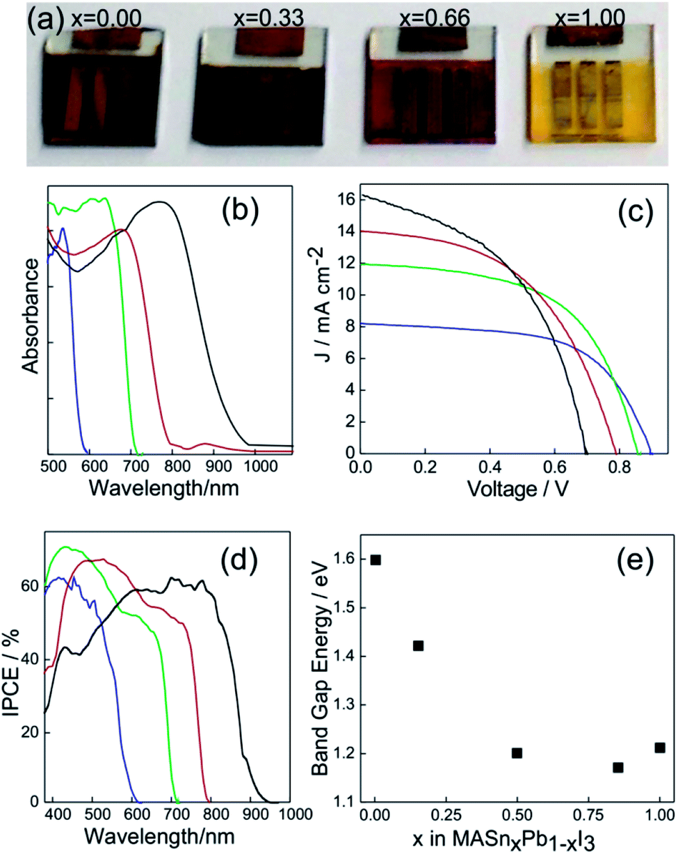 | ||
| Fig. 4 (a) Pictures of PSCs based on the MASn(I(1−x)Brx)3 composition, x being indicated in each solar cell. (b) Absorption spectra of MASn(I(1−x)Brx)3 layers with x = 0 (black line), x = 0.33 (red line), x = 0.66 (green line) and x = 1 (blue line). (c) and (d) Photocurrent density vs. voltage response and incident photon to charge carrier efficiency photocurrent respectively acquired for PSCs based on MASn(I(1−x)Brx)3. The color code was preserved from (b). (e) Band gap energy measured for perovskite layers prepared with different Sn/Pb ratios. Data were extracted from ref. 71 (a), (b), (c), (d) and (ref. 49), (e). Image reprinted with permission from ref. 71 (a) Copyright 2014 Nature Publishing Group. | ||
A similar situation is what we found when we analyzed the I/V curves of a series of PSCs made with these compounds (Fig. 4c). An increase in the iodide content produces higher current density with lower Voc. The IPCE spectrum (Fig. 4d) demonstrates that photons absorbed at lower energies could generate charge carriers as well as high energetic ones.
The crystalline structure of ABX3 perovskites also supports the gradual replacement of cation B(II). In order to study this effect on the optical properties, many research groups were able to prepare a series of mixed Sn/Pb perovskites synthesized from solution processing approaches.49,72–74 It is found that an increase in the content of Sn in the MAPbSnI3 perovskite follows an anomalous tendency of Vegard's law since a minimum in Ebg is obtained for a certain Pb/Sn composition (Fig. 4e). In this way, the Ebg of methylammonium iodide based perovskites can be tuned from 1.55 eV (pure lead) to 1.24 eV (pure Sn) whereas Ebg of the minimum is located at 1.18 eV. On the other hand, the lack of stability in an octahedral environment facilitates the oxidation from Sn(II) to Sn(IV).75 So, it seems that a minimum load of Pb(II) in the mix is necessary to stabilize the +2 oxidation state of Sn. The attempt to replace methyl ammonium by formamidinium (FASnI3) or cesium (CsSnI3) also helps to improve the stability, however photo-conversion efficiencies of these systems are close to 2.5%.76,77 In any case, encapsulation of the samples is needed to preserve the cell from oxidation.
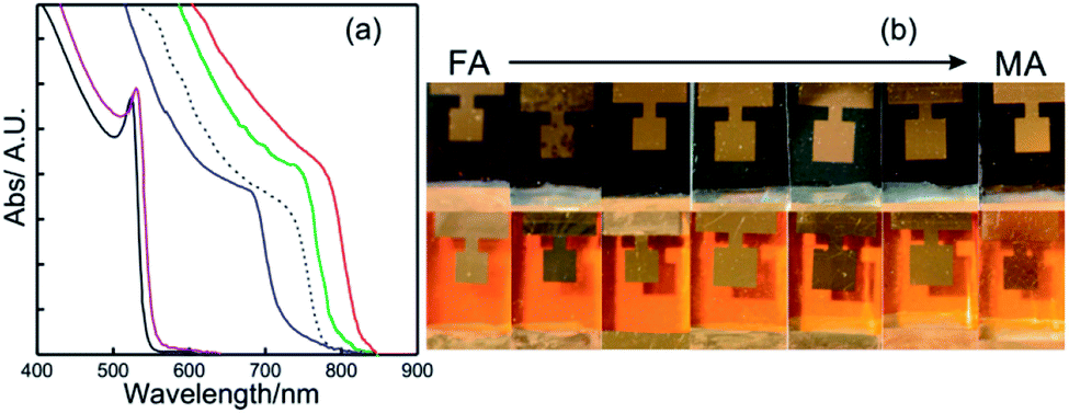 | ||
| Fig. 5 (a) Details of the absorption spectrum of APbX3 perovskite layers where A is cesium (solid red line with iodine), methyl ammonium (solid green line with iodine or solid violet line with bromide) or formamidinium (solid blue line with iodine or solid black line with bromide). The dashed black line represents the absorption profile of the ABX3 perovskite layer used in the champion cell. Data were extracted from ref. 81 and 82. (b) Images of a series of APbI3 (above) and APbBr3 (below) PSCs prepared with increasing MA/FA ratio (from left to right). Image adapted from ref. 83. Copyright 2016 Royal Society of Chemistry. | ||
This red-shift brings the Ebg of FAPI closer to the optimum single junction solar cell in terms of the Shockley Queisser limit. Fig. 5b shows a series of ABX3 PSCs prepared with different FA/MA ratios for bromide and iodide based lead compounds. It can be seen that the color variation in each halide series is almost negligible. On the other hand, the A cation is central to stabilize the perovskite crystalline phase and to minimize the photo-instability of ABX3 compounds. In other words, this stabilization prevents the crystallization of a non-perovskite phase (“yellow phase”), a polymorph of ABX3 perovskite that can co-exist once the synthesis occurs.84 As this phase is not photo-active, its formation must be avoided. Cesium based solar cells (CsPbI3) present higher stability against temperature, however photo-conversion efficiencies achieved with them did not surpass 5%.83,85 Previous research in this direction found that ternary or quaternary mixes of the three A cations mentioned above plus Rb were put together to obtain very high-efficient and stable ABX3 PSCs.86–88 The dashed line in Fig. 5a represents the absorption profile of one of these high-efficient and stable ABX3 layers.
To summarize this section, in Table 1 are shown the most relevant values for some PSCs described in this topic. It is important to mention that the tabulated values of the cells correspond to the average values.
| AMX3 type | E bg, eV | V oc, V | J sc, mA cm−2 | PCE | Stability | Solar cell configuration | Ref. |
|---|---|---|---|---|---|---|---|
| MAPbI3 | 1.55 | 0.93 | 19.10 | 11.25 | Poor | FTO/TiO2/PVK/spiro-OMeTAD/Au | 63 |
| MAPbBr3 | 2.34 | 1.20 | 2.94 | 2.5 | Stable | FTO/TiO2/PVK/spiro-OMeTAD/Au | 63 |
| FAPbI3 | 1.48 | 0.85 | 18.80 | 9.7 | Stable | FTO/TiO2/PVK/spiro-OMeTAD/Au | 81 |
| FAPbBr3 | 2.25 | 1.02 | 2.90 | 1.9 | Stable | FTO/TiO2/PVK/spiro-OMeTAD/Au | 81 |
| CsPbI3 | 1.73 | 0.80 | 12.10 | 2.9 | Stable | FTO/TiO2/PVK/spiro-OMeTAD/Au | 85 |
| MASnI3 | 1.28 | 0.59 | 17.80 | 3.2 | Very poor | ITO/PEDOT:PSS/PVK/PC61BM/Al | 74 |
| MASn0.8Pb0.2I3 | 1.19 | 0.66 | 20.20 | 6.5 | Very poor | ITO/PEDOT:PSS/PVK/PC61BM/Al | 74 |
| FASnI3 | 1.41 | 0.24 | 24.40 | 2.1 | Less stable | FTO/TiO2/PVK/spiro-OMeTAD/Au | 76 |
| CsSnI3 | 1.30 | 0.24 | 22.70 | 2.0 | Very poor | FTO/TiO2/PVK/spiro-OMeTAD/Au | 77 |
| [Rb5%(Cs5%MAFA95%)95%]PbI3 | 1.62 | 1.16 | 22.50 | 20.2 | Stable | FTO/TiO2/PVK/spiro-OMeTAD/PTAA/Au | 88 |
4. Semitransparent devices
Semi-transparent photovoltaic devices are gaining popularity since the addition of this functionality to the solar cells is a master key for their integration in BIPV and in tandem configurations.The new architectonic requirements prefer the use of glazing and windows in new buildings and installed devices must pose 25% of integrated transmittance (400–800 nm range).89 Specifically, a semitransparent device requires not only the partial transmission of the light in the mentioned spectral range but also the capability to generate images through the window integrated photovoltaic. This means that diffuse scattering of the light must be prevented across the solar cell layers and its interfaces. It can be considered that less than 5% of transmitted diffuse light discloses good visual images. This feature puts an emphasis onto the high transparency in the secondary elements of the cell like electron or hole selective layers and external contacts that normally absorb light in the blue or NIR region of the electromagnetic spectrum. A PSC normally uses a thin gold film as a back contact. However, the thickness of this layer strongly affects not only the photo-conversion efficiency but also the final appearance of the cell. This motivates the integration of perovskite photovoltaic devices with transparent electrodes based on indium tin oxide (ITO),90 dielectric–metal–dielectric layers,91 graphene92 or silver93 and carbon nano-wires.94 The latter examples are especially interesting regarding the development of full solution process management in the fabrication of solar cells. For detailed information on transparent electrodes in PSCs, we encourage the reader to follow ref. 35.
In addition to the demands of high transparency of the secondary elements of the cell, the high absorption coefficient of ABX3 perovskite layers leads to strong absorptions in the visible region of the electromagnetic spectrum. Thus, the simplest way to prepare semi-transparent devices is by decreasing the thickness of the planar active layer. However, this approach leads to a reduction in the photons absorbed by the cell, resulting in less efficient solar devices.95
Liquid processing by spin coating allows preparing ABX3 layers with different thicknesses simply by changing the concentration of precursors in the original dispersion or the spin coating parameters (final rotation speed or acceleration). In Fig. 6a is shown an image series that visually discloses the effect over the transparency when the thickness of a planar perovskite layer is gradually reduced. In Fig. 2b is presented the transmittance spectra for different ABX3 layer thicknesses. It can be seen that the transmittance of the layers is similar at wavelengths lower than 500 nm in most of the cases. In consequence, semitransparent cells present a gamut of brownish-orange colors.
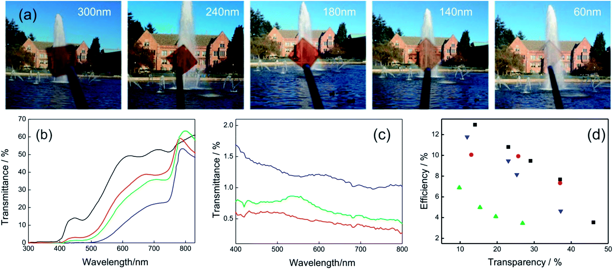 | ||
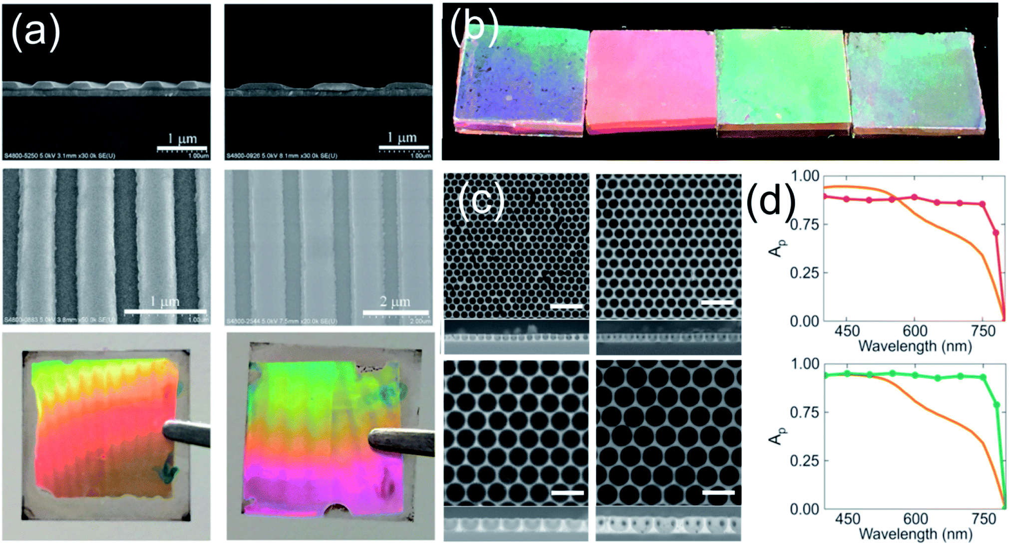
| Fig. 6 (a) Images obtained with MAPI films with different thicknesses (indicated in the upper part of each photograph) and supported on top of CuSCN/ITO coated glass. (b) Transmittance spectra of complete semitransparent solar cells that integrate MAPI layers of different thicknesses: 55 nm (black line), 105 nm (red line), 140 nm (green line), 290 nm (blue line). (c) Backward scattering of samples obtained with the method developed in ref. 96 for perovskite thickness of 80 nm (red line), 150 nm (green line) and 240 nm (blue line). (d) Efficiency of semitransparent perovskite solar cells against transparency (measured in the 400–800 nm spectral range) extracted from different methods reported in ref. 93 (black squares), ref. 91 (blue triangles), ref. 95 (red circles), ref. 97 (green triangles). Data were extracted from ref. 91 (b) and ref. 96 (c). Image reprinted with permission from ref. 95 (a) Copyright 2015 John Wiley and Sons. | ||
On the other hand, the deposition of smooth and continuous layers of ABX3 perovskites in the sub-150 nm thickness range is a challenge. A modification of the deposition method based on a solvent–solvent extraction protocol was proposed in order to obtain ABX3 layers as thin as 40 nm.93 Cells built with these layers present transparencies as high as 46% with efficiencies of 4%. Gas-assisted liquid processing also offers the opportunity to prepare smooth and continuous thin layers of ABX3 perovskites to control the transparency.91,96 The lack of roughness of the layers contributes to avoiding diffuse light scattering, improving the optical quality of the solar cells. Fig. 6c shows the backward scattering obtained for different thicknesses. Values lower than 2% are obtained in all cases indicating the high optical quality of samples.
The group of Prof. Snaith developed semitransparent devices using a strategy that allows controlling the perovskite of MAPI or FAPI film coverage. The method is based on the deposition of an ABX3 nano-island layer of 1 μm thickness by selecting an appropriate solvent and posterior thermal treatment.97,98 When the nanostructure coverage is high the perovskite film presents a black color thus transparency falls. If the separation between nano-islands increases, the ABX3 films look semi-transparent with a neutral color. Conversion efficiencies of 8% were achieved with a 30% transparent cell. However, PSCs that integrate nano-island layers could suffer deterioration in the photo-conversion efficiency because of the increase of the shunt resistance produced by a lack of interconnection in the absorbent material. Fig. 6d shows the photo-conversion efficiency obtained as a function of the transparency for PSCs that integrate semitransparent active layers developed by the different approaches presented so far.
Another technological characteristic that offers semitransparent PSCs is the possibility to harvest photons from the front and the rear sides of the cell as long as highly transparent counter-electrodes are used. This potential is a big advantage in terms of BIPV where indoor illumination or floor reflected light could reach the PSC from the rear side. Recent studies on this subject in PSCs have demonstrated that photo-conversion efficiencies obtained from back illumination can be as high as a 70% of the efficiency registered under front illumination.99,100Table 2 shows the typical parameters obtained for these semi-transparent PSCs.
| PVK thickness, nm | J sc, mA cm−2 | V oc, V | PCE | AVT | Stability | Solar cell configuration | Ref. |
|---|---|---|---|---|---|---|---|
| 140 | 9.2 | 1.07 | 7.33 | 37.5 | Acceptable | ITO/CuSCN/PVK/PCBM/bis-C60/Ag | 93 |
| 180 | 12.2 | 1.07 | 9.92 | 25.7 | Acceptable | ITO/CuSCN/PVK/PCBM/bis-C60/Ag | 93 |
| 240 | 13.0 | 1.07 | 10.06 | 13.0 | Acceptable | ITO/CuSCN/PVK/PCBM/bis-C60/Ag | 93 |
| 70 | 11.6 | 0.97 | 7.81 | 37.0 | n.e. | ITO/PEDOT:PSS/PVK/PCBM/bis-C60/ZnO/Ag | 91 |
| 100 | 14.2 | 0.98 | 9.55 | 29.0 | n.e. | ITO/PEDOT:PSS/PVK/PCBM/bis-C60/ZnO/Ag | 91 |
| 130 | 17.3 | 0.97 | 10.81 | 23.0 | n.e. | ITO/PEDOT:PSS/PVK/PCBM/bis-C60/ZnO/Ag | 91 |
| 370 | 19.1 | 0.97 | 12.65 | 14.0 | n.e. | ITO/PEDOT:PSS/PVK/PCBM/bis-C60/ZnO/Ag | 91 |
| 55 | 10 | 0.72 | 4.63 | 37.2 | n.e. | FTO/TiO2/PVK/spiro-OMeTAD/MoO3/Au/MoO3 | 92 |
| 110 | 14.0 | 0.94 | 8.15 | 25.3 | n.e. | FTO/TiO2/PVK/spiro-OMeTAD/MoO3/Au/MoO3 | 92 |
| 140 | 15 | 0.95 | 9.46 | 23.0 | n.e. | FTO/TiO2/PVK/spiro-OMeTAD/MoO3/Au/MoO3 | 92 |
| 280 | 20.0 | 0.99 | 11.78 | 11.9 | n.e. | FTO/TiO2/PVK/spiro-OMeTAD/MoO3/Au/MoO3 | 92 |
| Nanoisland | 9.5 | 0.70 | 6.10 | 17.0 | Unstable | FTO/TiO2/PVK-spiro-OMeTAD/Au | 94 |
| 275 | 16.50 | 0.95 | 12.30 | n.e. | Stable | ITO/PEDOT:PSS/PVK/PC60BM/Al:ZnO/ITO | 95 |
| 150 | 11.08 | 0.98 | 10.66 | n.e. | Stable | ITO/PEDOT:PSS/perovskite/PCBM/BCP/Ag | 90 |
| 240 | 16.6 | 1.02 | 6.87 | n.e. | Stable | ITO/PEDOT:PSS/perovskite/PCBM/BCP/Ag | 90 |
5. Tandem structures
The achievement in the efficiencies of semitransparent PSCs and the feasibility to modify their Ebg paved the way for integrating them in tandem solar cell systems as the top solar cell, as the bottom solar cell or in both positions (vide infra). A tandem system consists of a stack of two or more solar cells (normally two) where the upper cell absorbs the short wavelengths of the incoming radiation whereas the bottom cell absorbs the light that passes through the top cell without being absorbed. A theoretical design of a 2-terminal monolithic tandem architecture must consider the current matching between both cells in order to minimize recombinations.101A conscious design needs the optical constants of each element of the cell but in particular those that are related to the absorbing layers, which in short are the ones that will dictate the thicknesses of the films to be used in the device.
In contraposition, the design of a four-terminal tandem is less strict because each individual cell can be electrically isolated or connected in parallel. The Shockley–Queisser limit theory predicts, for the case of a double junction solar cell, Ebg values of 1.1 and 1.75 eV for the lower and upper cell respectively.
These values make MAPI based solar cells reliable candidates to act as the top cell (light shines firstly in this cell) whereas a silicon solar cell or a copper indium gallium selenide (CIGS) solar cell can be placed at the bottom.102 In many cases, the whole ensemble can be processed by solution processing methods.103
We mentioned in the previous sections of this review that the versatility in the composition of the ABX3 perovskites allows us to tune the Ebg between 3.11 eV and 1.15 eV.
This flexibility enables the fabrication of all PSC tandems placing two ABX3 layers with different bandgaps. For example, MAPbI and MAPbBr were employed as rear and front cells respectively to achieve a tandem structure that is capable of generating an open circuit voltage of 2.2 V.104 Additionally, a careful modelling of the tandem determines the use of mixed lead–tin based perovskites which can extend the absorption to the near infrared region.49 A 4-terminal configuration that mechanically stacks a bottom layer of (FASnI3)0.6(MAPbI3)0.4 as the low band-gap layer (Ebg = 1.25 eV) and a top layer of FA0.3MA0.7PbI3 (Ebg = 1.58 eV) achieved 21% photo-conversion efficiency.105
The aim of developing tandem cells is based on the opportunity to achieve operating voltages higher than 2.0 V that, in principle, can supply bias to other photo-electrochemical systems as water splitting or other advanced oxidation technologies.106–109
6. Structural color in perovskite solar cells
In a previous section, we showed that the color gamut of the ABX3 perovskite in PSCs can be tuned from red to yellowish orange by changing the chemical composition. This color modification leads to a decrease in photo-conversion efficiencies as bromide amount in the ABX3 layer increases. Therefore, a different strategy instead of chemical modification was needed to extend the color palette of the photovoltaic cell across the entire electromagnetic spectrum. These complementary methodologies are based on the integration of engineered nanostructures that confer color to the device through light interference phenomena.The initial approach was achieved by means of the integration of dielectric mirrors (Bragg mirrors) in the cell. These structures can selectively reflect a certain range of wavelengths to generate structural color. One advantage of this type of color is the lack of bleaching because no light absorption is produced. The most effective way to build a Bragg mirror is the alternate deposition of layers with different refractive indices (commonly SiO2 and TiO2) which provides the spatial modulation of the refractive indices.
The spectral range reflected can be tuned by modifying the thicknesses of SiO2 and TiO2 in the scaffold. A way to integrate that in MAPI PSCs is the use of a Bragg mirror with a large refractive index as a scaffold of controlled porosity allowing the infiltration by MAPI precursors.110,114 In this sense, a one dimensional photonic crystal acts as a scaffold that confers color to the photovoltaic device. Images of PSCs that include these photonic structures are disclosed in Fig. 7a. This approach uses a capping layer of perovskite as thick as reference cells (300 nm). As some part of the incident radiation is reflected and does not reach the cell, the efficiencies of these cells are lower than the reference one (10% vs. 13%).
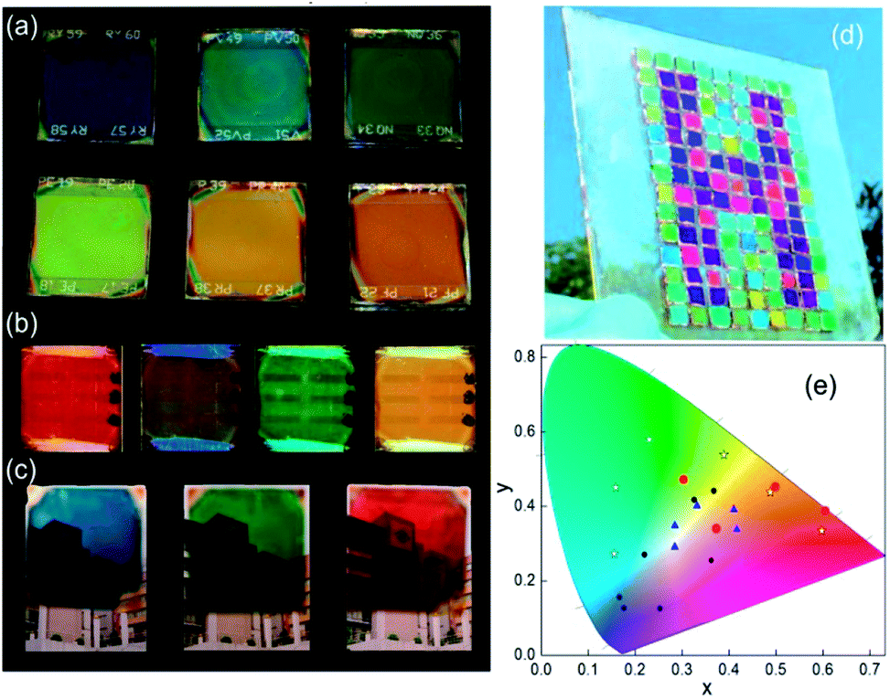 | ||
| Fig. 7 Images of a structural colored perovskite solar cell based on (a) distributed Bragg reflectors as the scaffold, (b) distributed Bragg reflectors on the back, (c) metal/dielectric/metal optical micro-cavities; (d) top layer thickness control approach; (e) CIE 1931 chromaticity diagram where color coordinates of the different methods described are indicated: DBR scaffold (blue triangles), DBR back (red circles) top layer control (black circles); optical cavity (white squares). Data adapted from ref. 110, 111, 112 and 113 respectively. Images reproduced with permission from ref. 111 (b), ref. 113 (c) and ref. 112 (d) Copyright 2016 (b, c, d) American Chemical Society. | ||
In another approach, the Bragg mirror is positioned on the back side of the cell and electrically isolated from the rest of the components.111 In this case, the dielectric structure (also made with TiO2 and SiO2 layers) acts as a selective mirror that can reflect back photons that passed without being absorbed in the active layer. This “second opportunity” absorption increases 10% the photo-conversion efficiencies. In these systems, a semi-transparent thin perovskite layer with a 40 nm thickness was used. Efficiencies of these cells are around 3.5–4.3% (transparencies between 28% and 12% depending on the design of the Bragg mirror) whereas when the thickness of the active layer is increased to 160 nm, efficiencies rise to 10.7–10.3% with a transparency of 4% (Fig. 7b).
Another approach that brings structural color to PSCs is the creation of an optical cavity. This arrangement consists of a dielectric layer sandwiched between two conductors or metals.113,115 A reliable configuration of this type of optical element is achieved by placing it as the counter electrode. In this way, optical cavities made with Ag/ITO/Ag or Ag/WO3/Ag were deposited on top of a hole-selective layer by physical vapor deposition methods. This method also uses semi-transparent layers (80 nm thickness) of perovskite to allow a transmittance window that can be spectrally tuned by modifying the thickness of the dielectric of the optical cavity. Photo-conversion efficiencies of these cells are close to 5%. Images of these colored semi-transparent cells can be found in Fig. 7c.
In a simpler but effective approach, Zhou and co-workers created efficient and colorful solar cells controlling the thickness of a PEDOT:PSS layer deposited on top of the cell by spin coating or by transferring the charge carrier selective layer with the help of PDMS112 (Fig. 7d). In this case, this layer acts as a charge carrier transport layer and as a spectral selective anti-reflection coating. A careful control of the thickness of PEDOT:PSS produces interference lobes that can be spectrally tuned to select the desired range of reflecting wavelengths.
Fig. 7e presents a summary of the color coordinates disclosed in a CIE 1931 chromaticity diagram. Different types of symbols represent the four different methodologies described above. It can be seen that a huge area of the CIE coordinates is covered by the mentioned techniques, however more efforts will be taken in order to extend the gamut. Table 3 lists the CIEs and photo-operative parameters of PSCs that include structural color as a novel function.
| CIE (x, y) | PVK thickness, nm | J sc, mA cm−2 | V oc, V | PCE | Color | Solar cell configuration | Ref. |
|---|---|---|---|---|---|---|---|
| (0.39, 0.29) | 200 | 18.7 | 1.08 | 12.8 | Red | FTO/c-TiO2/m-TiO2/PVK/spiro-OMeTAD/PEDOT:PSST | 112 |
| (0.27, 0.25) | 200 | 19.3 | 1.11 | 15.2 | Purple | FTO/c-TiO2/m-TiO2/PVK/spiro-OMeTAD/PEDOT:PSST | 112 |
| (0.25, 0.35) | 200 | 19.2 | 1.11 | 15.1 | Cyan | FTO/c-TiO2/m-TiO2/PVK/spiro-OMeTAD/PEDOT:PSST | 112 |
| (0.32, 0.39) | 200 | 19.3 | 1.11 | 15.2 | Cyan-greenish | FTO/c-TiO2/m-TiO2/PVK/spiro-OMeTAD/PEDOT:PSST | 112 |
| (0.41, 0.40) | 200 | 19 | 1.11 | 15.4 | Green | FTO/c-TiO2/m-TiO2/PVK/spiro-OMeTAD/PEDOT:PSST | 112 |
| (0.55, 0.40) | 160 | 14.4 | 0.97 | 9.7 | Red | ITO/PEDOT:PSS/PVK/PC60BM/ZnO/Ag/dielectric mirror | 111 |
| (0.42, 0.40) | 160 | 15.3 | 0.97 | 10.3 | Blue | ITO/PEDOT:PSS/PVK/PC60BM/ZnO/Ag/dielectric mirror | 111 |
| (0.32, 0.50) | 160 | 15.5 | 0.97 | 10.5 | Light-blue | ITO/PEDOT:PSS/PVK/PC60BM/ZnO/Ag/dielectric mirror | 111 |
| (0.52, 0.44) | 160 | 15.7 | 0.97 | 10.7 | Yellow | ITO/PEDOT:PSS/PVK/PC60BM/ZnO/Ag/dielectric mirror | 111 |
| (0.6, 0.35) | 75 | 14.8 | 0.84 | 6.7 | Reddish-orange | ITO/PEDOT:PSS/PVK/PC61BM/Ag/ITO/Ag | 113 |
| (0.49, 0.45) | 75 | 14.1 | 0.88 | 7.2 | Orange | ITO/PEDOT:PSS/PVK/PC61BM/Ag/ITO/Ag | 113 |
| (0.39, 0.55) | 75 | 14.5 | 0.91 | 4.2 | Yellow | ITO/PEDOT:PSS/PVK/PC61BM/Ag/ITO/Ag | 113 |
| (0.23, 0.58) | 75 | 13.8 | 0.87 | 6.1 | Yellow-green | ITO/PEDOT:PSS/PVK/PC61BM/Ag/ITO/Ag | 113 |
| (0.15, 0.45) | 75 | 14.5 | 0.89 | 6.9 | Yellowish-green | ITO/PEDOT:PSS/PVK/PC61BM/Ag/ITO/Ag | 113 |
| (0.15, 0.27) | 75 | 14.7 | 0.85 | 7.6 | Bluish-green | ITO/PEDOT:PSS/PVK/PC61BM/Ag/ITO/Ag | 113 |
| (0.41, 0.34) | 300 | 7.2 | 0.91 | 4.1 | Red | FTO/TiO2/dielectric mirror/PVK/spiro-OMeTAD/Au | 110 |
| (0.41, 0.40) | 300 | 8.9 | 0.91 | 5.4 | Orange | FTO/TiO2/dielectric mirror/PVK/spiro-OMeTAD/Au | 110 |
| (0.33, 0.41) | 300 | 9.4 | 0.92 | 6.1 | Green | FTO/TiO2/dielectric mirror/PVK/spiro-OMeTAD/Au | 110 |
| (0.29, 0.35) | 300 | 10.1 | 0.93 | 6.5 | Blue-green | FTO/TiO2/dielectric mirror/PVK/spiro-OMeTAD/Au | 110 |
| (0.39, 0.30) | 300 | 12.1 | 0.94 | 7.6 | Blue | FTO/TiO2/dielectric mirror/PVK/spiro-OMeTAD/Au | 110 |
7. Integration of nanostructures in perovskite solar cells
The integration of nanostructures in solar cells is motivated by the aim to manage and deliver light to the absorbing layer in a highly efficient way.116 The different strategies carried out consist in the integration of metallic117 or dielectric nanostructures118 (nanoparticles, textured surfaces, etc.) in different solar cells. PSCs are not an exception for application of these approaches and nowadays, light management is an active field of research in PSCs. Although the MAPI perovskite is an excellent absorber in almost the whole of the visible electromagnetic spectrum, the integration of nanostructures could be beneficial in terms of decreasing the thickness of the absorber layer without losing the efficiency. This concept presents relevance for environmental safety applications since the quantity of a heavy metal like lead can be reduced if light is delivered in an efficient way to the absorbing layer into the cell. On the other hand, theoretical simulations or calculations are nowadays an indispensable tool to predict or verify the spatial and spectral distribution of electromagnetic field when sub-micrometer-structures are coupled to optoelectronic devices. Without any theoretical approach it is very difficult to assign univocally the observed experimental effects and how they are related to the enhancement of the performance of PSCs.7.1 Structuring perovskite layers
The simplest method that takes advantage of nanostructures is the use of external attachments with anti-reflective properties. These systems are based on arrays of nano-periodical elements based on a PDMS (polydimethylsiloxane) nanopyramid film obtained by soft-lithography. This film is mechanically attached onto the external side of the optical transparent electrode and serves as an anti-reflective coating as well as a self-cleaning structure.119,120 This approach is useful to improve efficiencies in flexible PSC systems where the ABX3 perovskite layer cannot be too thick.121More complexity is required when the active perovskite layer itself is the one to be patterned. Direct patterning of the perovskite by electron beam or similar techniques must be avoided owing to the thermal instability produced by the increase in the temperature of the microenvironment of the ABX3 perovskite layer as a consequence of the impinging of the patterning beam.122 Instead of these, soft lithographic methods are largely preferred in order to reduce the damage to the ABX3 film. Briefly, a master that contains a nanostructured periodic array is replicated negatively in a polymer. Then, this soft copy is transferred to a thin film using pressure and temperature. Some of the different solvents used in the photolithographic process (which is the most common technique to pattern surfaces) extremes the cautions to prevent the degradation of the ABX3 films. However, the chemical incompatibility of the perovskite with the use of DMSO as the solvent of perovskite precursors permits the patterning of an ABX3 spin coated freshly deposited film.123 The high boiling point of DMSO leads to a gel film plausible to be stamped with a previously patterned elastomer. The subsequent thermal process completes the conversion to a crystalline patterned ABX3 structure that preserves the electronic properties of the untreated layer. In a recent approach, Choy et al. demonstrated that the quality of the patterned perovskite film can be improved by the introduction of methyl amine gas into the voids of the pattern124 (see Fig. 8a). Likewise, they demonstrated that the optical absorption is spectrally enhanced when the perovskite layer is patterned. A similar micro-stamping procedure was used to create a 2D photonic structure with a previously deposited ABX3 perovskite film.126
 | ||
| Fig. 8 (a) Nanopatterning of a perovskite layer by the soft lithography method. Images disclose (from top to bottom) the cross-section, top view of the patterned perovskite and optical photograph of layers with gratings of 700 nm (left) and 1500 nm (right). (b) Images of different perovskite layers prepared through the infiltration of a polystyrene template and posterior removal. The size of the spheres is (from left to right): 700, 1000, 1800 and 2000 nm. (c) Top view and cross-sectional SEM images of different films prepared with the sphere sizes described in (c) (scale bar 3 μm). (d) Theoretical absorption spectrum of a perovskite layer that integrated gold (red line, upper panel) and silver (green line, bottom panel) nanoparticles with a radius of 120 nm and 130 nm, respectively. The orange line represents the absorption of a 300 nm perovskite layer. Images reproduced with permission from ref. 124. (a) Copyright (2017) John Wiley and Sons, ref. 125 (b, c) and ref. 41 (d) Copyright (2016) American Chemical Society. | ||
Furthermore, other synthesis methods lead to a periodical array of ABX3 perovskites. A three-dimensional or two-dimensional structural arrangement of a perovskite layer can be prepared using sacrificial arrays of polystyrene microspheres.125,127 Although the process has been successfully implemented, it is still necessary to improve the optical quality of the ABX3 layers. Another approach uses an ordered SiO2 scaffold to template the ABX3 perovskite that is synthesized within the pores by infiltrating the liquid precursors in the porous structure.81,128 The open and inter-connected porosity of the oxide layer facilitates the process that results in the total infiltration of the voids. This particular method confers transparency to the device surpassing the photo-conversion efficiencies achieved by the nanoisland approach (vide supra).
Other approaches involve the patterning of the selective charge carrier transporting layers also by soft-lithography techniques. Different periodic motifs reproducing flowers129 or moth eyes130 were molded on the ETL layer (TiO2 layer). Paetzold et al. demonstrated that the inner face of the frontal glass can be patterned,131 and this motif is preserved even after the deposition of ITO and ETL. In all cases solar cells that incorporate these motifs present an enhancement in photo-conversion efficiencies that can be attributed to antireflection effects, diffuse scattering or diffraction of light. Finally, a doctor-blade coating technique132 was used to structure a perovskite layer in a periodic array of polygons that produce colorful motifs by interference phenomena.
7.2 Particle inclusion
Dielectric sub-micron particles have been embedded in the mesoporous TiO2 layer inducing an increase of the diffusive scattering and also enhancement of the light absorbed in the perovskite layer in the 550 nm < λ < 750 nm range.133 However, this field remains almost unexplored and more exhaustive theoretical models and calculations are needed in order to clarify essential aspects of particle scattering and their effect on the near and far electromagnetic field.134 Metallic nanoparticles are also proposed to be included either in the active layer or in the secondary layers of the PSC.135 Silver nanoparticles as well as gold nanoparticles are candidates since strong localized plasmonic resonances can be supported on the surface of these particles providing an enhancement of the electromagnetic field.136Fig. 8d shows a theoretical calculation that shows the absorption enhancement in a PSC produced by the integration of metallic particles within the ABX3 perovskite layer. Perovskite solvent compatible metal particle synthesis or surface protection needs to be developed in order to match both systems.8. Surface passivation of ABX3 perovskite layers
Most of the solution process syntheses of ABX3 films lead to a polycrystalline material where the presence of under-coordinated ions arises at the surface of the crystal or at grain boundaries. Depending on the preparation method, ABX3 perovskites with halide enrichment or depletion in the surface can be obtained.137 These trap states can reduce the performance of PSCs via the accumulation of charge at the interface between the active and the charge carrier selective layers. In addition, the environmental instability of perovskite layers affects the photo-conversion efficiencies by different mechanisms that degrade the ABX3 layer in the presence of oxygen, moisture or UV light. Some of these reactive pathways are triggered by the aforementioned surface defects or trap states.138 The high trap densities and the strong lattice deformation also affect the optical properties of the surface that can strongly differ from its bulk counterparts.139 Both situations clearly indicate that a control of the nanostructured ABX3 perovskite is needed in the seeking of more efficient photovoltaic devices. One approach is directed at controlling the morphology of perovskites to produce defect-free perovskite layers.140,141 Progress in this direction deserves meticulous reviewing that exceeds the scope of this manuscript. Another approach consists in the use of passivation ligands that once coordinated at the surface of ABX3 grains normalize the charge density and release the strain. This occurs by a compensation of the under-coordinated atoms at the surface (halides or center metals). In this way the stability of the layer is improved.142 Perovskite layers are easy to functionalize: molecules that serve as passivating agents are mixed together (in situ approach) with the perovskite precursors or dissolved in a solvent in which the ABX3 perovskite is insoluble (chlorobenzene, toluene, etc.). In the latter case, the functionalizers are grafted to the perovskite layer by wet deposition methods (either dip or spin coating) (ex situ approach). As we mentioned before, the different types of traps require different molecules and methods to functionalize the surface. Electrophilic compounds like iodopentafluorobenzene or fullerene derivatives are Lewis acids that can passivate the excess of halide at the perovskite surface (Lewis basic traps).143,144 In consequence, this surface passivation is conducive to an enhancement in the efficiency of PSCs and suppression of the hysteresis in illuminated cyclic voltammetry since the hole trapping is inhibited and the electron extraction is improved (Fig. 9a).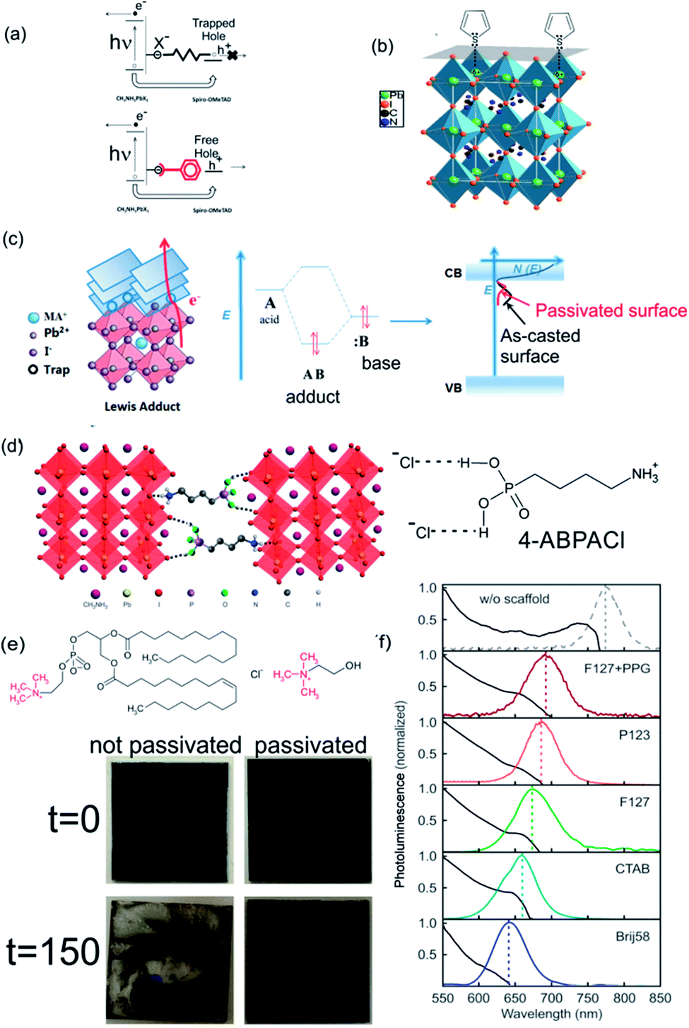 | ||
| Fig. 9 Scheme of the surface passivation processes that take place under (a) Lewis acid or Lewis base passivation via (b) thiophene or (c) adduct formation over MAPI. (d) Scheme of the cross-linking effect of 4-butylphosphonic acid ammonium chloride (4-ABPACl) over a MAPI perovskite. (e) Alkylammonium molecules used to passivate ABX3 layers. Below: images of treated (right) and untreated layers (left) before and after exposure at 90% humidity (treatment time is indicated in the left). (f) Emission of MAPI nanocrystals confined in nanostructured porous layers templated with different sizes (size decreases from the top to bottom spectra). Images reproduced with permission from ref. 143 (a), ref. 145 (b) Copyright (2014) American Chemical Society, ref. 147 (c) Copyright (2017) John Wiley and Sons, ref. 148 (d), ref. 149 (e) Copyright 2015, 2017 Nature Publishing Group, ref. 150 (f) Copyright (2017) John Wiley and Sons. | ||
Thiophene and pyridine molecules were also used as passivating agents of Lewis acid traps (halide defects). In this case, both molecules are employed as Lewis bases that are coordinated to Pb atoms located at the surface of ABX3 polycrystalline film (Fig. 9b).145,146 π–π conjugates can also coordinate at halide vacancies forming an adduct between them and acid vacancies improving the electron extraction as the band defects shift to energies near the conduction band of ABX3 perovskites (Fig. 9c). However, these strategies are directed at passivating only one type of defects. A “one-pot” approach based on tertiary and quaternary ammonium halides can passivate both sites using the same treatment, improving the conversion efficiencies and conferring stability to the cell on exposure to humidity.149,151 This effect is disclosed in Fig. 9e where images of samples with and without passivation treatment (right and left respectively) before and after being illuminated and exposed at 90% of humidity (above and below respectively) are compared. No degradation occurs in the sample with passivation treatment. Zhang et al. developed, in another approach, a bi-functional ligand as a short chain peptide to passivate both types of under-coordinated sites in perovskite nanocrystals. Negatively charged carboxylate and positively charged ammonium groups coordinate at B2+ and X− sites respectively.152 Graetzel et al. used a crosslinking agent (alkylphosphonic acid ω-ammonium chloride) that coordinates with neighboring ABX3 octahedra and shields the film from water (Fig. 9d).148
Optical properties are also benefited from the aforementioned treatments. As the recombination centers are annihilated, the non-radiative de-excitation rate is dramatically reduced improving the scope of increasing the quantum efficiencies of the radiative process (i.e. electro- and/or photo-emission) that also affects the efficiency of the PSC.153
Colloidal chemistry synthesis of ABX3 perovskites is also a very active field which deserves an in-depth review. However, I would like to highlight another strategy to protect the surface of nanocrystals based on their embedment in a porous matrix. In this approach, the synthesis of the perovskite nanocrystals is done within the porous network. As the size of the ABX3 nanocrystals is governed by the pore size of the matrix, their optical properties are modified according to the quantum confinement regime.150Fig. 9f shows how the emission band of MAPI is shifted to lower wavelengths as the pore size of the network is reduced. This method allows obtaining layers of isolated ABX3 perovskite nanocrystals with a reduced density of bulk traps that would be beneficial to their optoelectronic properties.
9. Conclusions and outlook
The high efficiencies of ABX3 PSCs indicate that they have arrived here to stay. Their impressive efficiencies mobilize a strong interest in the photovoltaics field where optical properties play a significant role. The ease of playing from the solution side with the ABX3 perovskite composition brings a unique opportunity for tailoring the bandgap “a la carte”, which is meaningful for a myriad of photovoltaics design. In that sense, ABX3 perovskite materials are advantageous against other types of photovoltaic active materials where the Ebg is directed by the structure of the absorber as in silicon solar cells (multicrystalline, crystalline or amorphous) or by the nature of the absorber (dye in DSSCs, substituted polymers in organic solar cells). In the latter case, the light absorption profile is conditioned by future developments in organometallic synthesis. Furthermore, the judicious control of ABX3 perovskite layer thickness by liquid deposition methods allows bringing optional functionalities to the cell such as structural color or semitransparency. Both characteristics are very important when a reliable technology oriented to BIPV is sought. Both mentioned functionalities are very difficult to implement with Si or CIGS cells. Semitransparency and Ebg tunability enable the use of ABX3 as the top cell, bottom cell or both in tandem configurations opening an interesting way to surpass the Shockley Queisser limit and to increase the photovoltage. Finally, the wide range of operational thicknesses achievable with ABX3 layers (20–500 nm) combined with their large diffusion lengths is another instrument to the optical design of the PSCs via thin layer constructive/destructive interference effects. This type of approach is not suitable for other cell types, including organic or Q-dot solar cells where the thickness of the active layer cannot be larger than certain values. In addition, the ABX3 perovskite is a unique semiconductor that permits via liquid processing its structuration, modification or incorporation of different optical microstructural features to modify the absorption profile.Despite these advantages and improvements at the lab scale, there are substantial issues that need to be addressed to achieve a mature and well-consolidated technology. PSCs with large area and improved stability are needed when outdoor performance is required. In both cases, the optical properties of the ensemble play a fundamental role. On one hand, the search of stable ABX3 perovskites has found a promising pathway by modifying their composition. A thorough optical analysis of these new composition perovskites is mandatory in order to design PSCs with optimized performance. Additionally, the stability of the PSCs can also be improved by the encapsulation of the entire device. The judicious design of these protective elements can be done from an optical point of view to improve the delivery of photons to the active layer. Encapsulates that integrate antireflective elements, diffraction gratings, light scattering centers or down converters are options to be considered once the inclusion of a protective layer is mandatory. An angular analysis of the response of these structures must be carried out when applications in BIPV are the target.
On the other hand, it was usually demonstrated that the photo-conversion efficiency of large area PSCs is lower than that of square millimeter lab devices. Several problems associated with charge carrier diffusion in ABX3 thicker layers have prevented its use at large scales. Some of the strategies presented in this review will help to improve the performance of these large area elements assuring an aesthetical functionality or maximizing the optical absorption in the core of the PSCs.
Conflicts of interest
There are no conflicts to declare.Acknowledgements
I would like to acknowledge Dr G. Arzac, Dr H. Miguez and M. Anaya for reading and commenting on this manuscript. This research has received funding from the Spanish Ministry of Economy and Competitiveness under Grant No. MAT2014-54852-R. The research leading to these results had received funding from the European Research Council under the European Union's Seventh Framework Programme (FP7/2007–2013)/ERC Grant Agreement No. 307081 (POLIGHT).Notes and references
-
U.S. Energy Information Administration, International Energy Outlook 2016, 2016, vol. 0484 Search PubMed
.
-
P. Würfel, Physics of Solar Cells: from Principles to New Concepts, 2007 Search PubMed
-
U.S. Energy Information Administration, Monthly Energy Review, November 2016 Search PubMed
- W. Wang, M. O. Tadé and Z. Shao, Chem. Soc. Rev., 2015, 44, 5371–5408 RSC
- V. Siva Reddy, S. C. Kaushik, K. R. Ranjan and S. K. Tyagi, Renewable Sustainable Energy Rev., 2013, 27, 258–273 CrossRef
- M. M. Lee, J. Teuscher, T. Miyasaka, T. N. Murakami and H. J. Snaith, Science, 2012, 338, 643–647 CrossRef CAS PubMed
- A. Kojima, K. Teshima, Y. Shirai and T. Miyasaka, J. Am. Chem. Soc., 2009, 131, 6050–6051 CrossRef CAS PubMed
- NREL, Best Res. Effic., http//www.nrel.gov, accessed June 2017.
- M. Cai, Y. Wu, H. Chen, X. Yang, Y. Qiang and L. Han, Adv. Sci., 2017, 4, 1600269 CrossRef PubMed
- C. Wehrenfennig, G. E. Eperon, M. B. Johnston, H. J. Snaith and L. M. Herz, Adv. Mater., 2014, 26, 1584–1589 CrossRef CAS PubMed
- Z.-K. Tan, R. S. Moghaddam, M. L. Lai, P. Docampo, R. Higler, F. Deschler, M. Price, A. Sadhanala, L. M. Pazos, D. Credgington, F. Hanusch, T. Bein, H. J. Snaith and R. H. Friend, Nat. Nanotechnol., 2014, 9, 687–692 CrossRef CAS PubMed
- G. Xing, N. Mathews, S. S. Lim, N. Yantara, X. Liu, D. Sabba, M. Grätzel, S. Mhaisalkar and T. C. Sum, Nat. Mater., 2014, 13, 476–480 CrossRef CAS PubMed
- L. Dou, Y. M. Yang, J. You, Z. Hong, W.-H. Chang, G. Li and Y. M. Yang, Nat. Commun., 2014, 5, 5404 CrossRef CAS PubMed
- M. Schreier, L. Curvat, F. Giordano, L. Steier, A. Abate, S. M. Zakeeruddin, J. Luo, M. T. Mayer and M. Grätzel, Nat. Commun., 2015, 6, 7326 CrossRef CAS PubMed
- W. Xu, F. Li, Z. Cai, Y. Wang, F. Luo and X. Chen, J. Mater. Chem. C, 2016, 4, 9651–9655 RSC
- T. Song, Q. Chen, H. H.-P. Zhou, C. Jiang, H.-H. Wang, Y. Yang, Y. Liu, J. You and Y. Yang, J. Mater. Chem. A, 2015, 3, 9032–9050 CAS
- Y. Zhao and K. Zhu, J. Phys. Chem. Lett., 2014, 5, 4175–4186 CrossRef CAS PubMed
- N. J. Jeon, J. H. Noh, Y. C. Kim, W. S. Yang, S. Ryu and S. Il Seok, Nat. Mater., 2014, 13, 1–7 Search PubMed
- M. Yoshimura, W. L. Suchanek and K. Byrappa, MRS Bull., 2000, 25, 17–25 CrossRef CAS
- J. Albero, A. R. Malik and H. Garcia, J. Mater. Chem. A, 2016, 4, 4353–4364 CAS
- S.-G. Li, K.-J. Jiang, M.-J. Su, X.-P. Cui, J.-H. Huang, Q.-Q. Zhang, X.-Q. Zhou, L.-M. Yang and Y.-L. Song, J. Mater. Chem. A, 2015, 3, 9092–9097 CAS
- J.-W. Lee, S.-I. Na and S.-S. Kim, J. Power Sources, 2017, 339, 33–40 CrossRef CAS
- G. Cotella, J. Baker, F. DeRossi, C. Pleydell-Pearce, M. Carnie and T. Watson, Sol. Energy Mater. Sol. Cells, 2017, 159, 362–369 CrossRef CAS
- K. Hwang, Y. S. Jung, Y. J. Heo, F. H. Scholes, S. E. Watkins, J. Subbiah, D. J. Jones, D. Y. Kim and D. Vak, Adv. Mater., 2015, 27, 1241–1247 CrossRef CAS PubMed
- B. Luo, S. Bonabi Naghadeh and J. Zhang, ChemNanoMat, 2017, 95064, 1–11 Search PubMed
- Q. Shen, Y. Ogomi, J. Chang, S. Tsukamoto, K. Kukihara, T. Oshima, N. Osada, K. Yoshino, K. Katayama, T. Toyoda and S. S. Hayase, Phys. Chem. Chem. Phys., 2014, 16, 19984 RSC
- N. G. Park, Mater. Today, 2015, 18, 65–72 CrossRef CAS
- H.-S. Kim, I. Mora-Sero, V. Gonzalez-Pedro, F. Fabregat-Santiago, E. J. Juarez-Perez, N.-G. Park and J. Bisquert, Nat. Commun., 2013, 4, 2242 Search PubMed
- Q. G. Du, G. Shen and S. John, AIP Adv., 2016, 6, 065002 CrossRef
- S. D. Stranks and H. J. Snaith, Nat. Nanotechnol., 2015, 10, 391–402 CrossRef CAS PubMed
- L. M. Pazos-Outon, M. Szumilo, R. Lamboll, J. M. Richter, M. Crespo-Quesada, M. Abdi-Jalebi, H. J. Beeson, M. Vruini, M. Alsari, H. J. Snaith, B. Ehrler, R. H. Friend and F. Deschler, Science, 2016, 351, 1430–1433 CrossRef CAS PubMed
- G. Kang, J. Yoo, J. Ahn and K. Kim, Nano Today, 2015, 10, 22–47 CrossRef CAS
- X. Zheng and L. Zhang, Energy Environ. Sci., 2016, 9, 2511–2532 CAS
- A. Henemann, Renewable Energy Focus, 2008, 9(14), 16–19 Search PubMed
- K. T. Lee, L. J. Guo and H. J. Park, Molecules, 2016, 21, 1–21 Search PubMed
- A. Poglitsch and D. Weber, J. Chem. Phys., 1987, 87, 6373 CrossRef CAS
- D. B. Mitzi, C. A. Feild, W. T. A. Harrison and A. M. Guloy, Nature, 1994, 369, 467–469 CrossRef CAS
- J.-H. Im, C.-R. Lee, J.-W. Lee, S.-W. Park and N.-G. Park, Nanoscale, 2011, 3, 4088 RSC
- G. Lozano, S. Colodrero, O. Caulier, M. E. Calvo and H. Míguez, J. Phys. Chem. C, 2010, 114, 3681–3687 CAS
- M. A. Green, Y. Jiang, A. M. Soufiani and A. Ho-Baillie, J. Phys. Chem. Lett., 2015, 6, 4774–4785 CrossRef CAS PubMed
- S. Carretero-Palacios, A. Jiménez-Solano and H. Míguez, ACS Energy Lett., 2016, 1, 323–331 CrossRef CAS PubMed
- Q. Lin, A. Armin, R. C. R. Nagiri, P. L. Burn and P. Meredith, Nat. Photonics, 2014, 9, 106–112 CrossRef
- P. Loeper, M. Stuckelberger, B. Niesen, J. Werner, M. Filipic, S.-J. Moon, J.-H. Yum, M. Topic, S. De Wolf and C. Ballif, J. Phys. Chem. Lett., 2015, 6, 66–71 CrossRef PubMed
- C.-Y. C.-W. Chen, S.-Y. Hsiao, C.-Y. C.-W. Chen, H.-W. Kang, Z.-Y. Huang and H.-W. Lin, J. Mater. Chem. A, 2015, 3, 9152–9159 CAS
- J. M. Ball, S. D. Stranks, M. T. Hörantner, S. Hüttner, W. Zhang, J. W. Crossland, I. Ramirez, M. Riede, M. B. Johnston, U. Steiner, J. Henry, E. J. W. Crossland, I. Ramirez, M. Riede, M. B. Johnston, R. H. Friend and H. J. Snaith, Energy Environ. Sci., 2015, 8, 602–609 CAS
- L. J. Phillips, A. M. Rashed, R. E. Treharne, J. Kay, P. Yates, I. Z. Mitrovic, A. Weerakkody, S. Hall and K. Durose, Sol. Energy Mater. Sol. Cells, 2015, 147, 327–333 CrossRef
- E. A. Irene, Thin Solid Films, 1993, 233, 96–111 CrossRef CAS
- D. Poelman and P. F. Smet, J. Phys. D: Appl. Phys., 2003, 1850, 1850–1857 CrossRef
- M. Anaya, J. P. Correa-Baena, G. Lozano, M. Saliba, P. Anguita, B. Roose, A. Abate, U. Steiner, M. Grätzel, M. E. Calvo, A. Hagfeldt and H. Míguez, J. Mater. Chem. A, 2016, 60–61, 269 Search PubMed
- M. Anaya, G. Lozano, M. E. Calvo, W. Zhang, M. B. Johnston, H. J. Snaith and H. Miguez, J. Phys. Chem. Lett., 2015, 6, 48–52 CrossRef CAS PubMed
- J. A. Guerra, A. Tejada, L. Korte, L. Kegelmann, J. A. Töfflinger, S. Albrecht, B. Rech and R. Weingärtner, J. Appl. Phys., 2017, 121, 173104 CrossRef
- M. Shirayama, H. Kadowaki, T. Miyadera, T. Sugita, M. Tamakoshi, M. Kato, T. Fujiseki, D. Murata, S. Hara, T. N. Murakami, S. Fujimoto, M. Chikamatsu and H. Fujiwara, Phys. Rev. Appl., 2016, 5, 1–25 Search PubMed
- S. Brittman and E. C. Garnett, J. Phys. Chem. C, 2016, 120, 616–620 CAS
- R. A. Kerner, L. Zhao, Z. Xiao and B. P. Rand, J. Mater. Chem. A, 2016, 4, 8308–8315 CAS
- N. K. Noel, S. N. Habisreutinger, B. Wenger, M. T. Klug, M. T. Hörantner, M. B. Johnston, R. J. Nicholas, D. T. Moore and H. Snaith, Energy Environ. Sci., 2017, 10, 145–152 CAS
- M. S. Alias, I. Dursun, M. I. Saidaminov, E. M. Diallo, P. Mishra, T. K. Ng, O. M. Bakr and B. S. Ooi, Opt. Express, 2016, 24, 16586 CrossRef PubMed
- J.-H. Chang, H.-F. Wang, W.-C. Lin, K.-M. Chiang, K.-C. Chen, W.-C. Huang, Z.-Y. Huang, H.-F. Meng, R.-M. Ho and H.-W. Lin, J. Mater. Chem. A, 2014, 2, 13398 CAS
- G. F. Burkhard, E. T. Hoke and M. D. McGehee, Adv. Mater., 2010, 22, 3293–3297 CrossRef CAS PubMed
- L. A. A. Pettersson, L. S. Roman and O. Inganäs, J. Appl. Phys., 1999, 487, 487–496 CrossRef
- Q. Chen, N. De Marco, Y. Yang, T. Bin Song, C. C. Chen, H. Zhao, Z. Hong, H. Zhou and Y. Yang, Nano Today, 2015, 10, 355–396 CrossRef CAS
- E. H. Sargent, R. Comin, E. Thibau, G. Walters, O. Voznyy and Z. Lu, J. Mater. Chem. C, 2015, 3, 8839–8843 RSC
- J. H. Noh, S. H. Im, J. H. Heo, T. N. Mandal and S. Il Seok, Nano Lett., 2013, 13, 1764–1769 CrossRef CAS PubMed
- D. Cui, Z. Yang, D. Yang, X. Ren, Y. Liu, Q. Wei, H. Fan, J. Zeng and S. Liu, J. Phys. Chem. C, 2015, 120, 42–47 Search PubMed
- R. E. Beal, D. J. Slotcavage, T. Leijtens, A. R. Bowring, R. A. Belisle, W. H. Nguyen, G. Burkhard, E. T. Hoke and M. D. McGehee, J. Phys. Chem. Lett., 2016, 7, 746–751 CrossRef CAS PubMed
- F. C. Hanusch, E. Wiesenmayer, E. Mankel, A. Binek, P. Angloher, C. Fraunhofer, N. Giesbrecht, J. M. Feckl, W. Jaegermann, D. Johrendt, T. Bein and P. Docampo, J. Phys. Chem. Lett., 2014, 5, 2791–2795 CrossRef CAS PubMed
- D. P. McMeekin, G. Sadoughi, W. Rehman, G. E. Eperon, M. Saliba, M. T. Horantner, A. Haghighirad, N. Sakai, L. Korte, B. Rech, M. B. Johnston, L. M. Herz and H. J. Snaith, Science, 2016, 351, 151–155 CrossRef CAS PubMed
- A. Babayigit, A. Ethirajan, M. Muller and B. Conings, Nat. Mater., 2016, 15, 247–251 CrossRef CAS PubMed
- F. Giustino and H. J. Snaith, ACS Energy Lett., 2016, 1, 1233–1240 CrossRef CAS
- G.-T. Wang, J.-H. Wei and Y.-F. Peng, AIP Adv., 2016, 6, 65213 CrossRef
- F. Hao, C. C. Stoumpos, R. P. H. Chang and M. G. Kanatzidis, J. Am. Chem. Soc., 2014, 136, 8094–8099 CrossRef CAS PubMed
- F. Hao, C. C. Stoumpos, D. H. Cao, R. P. H. Chang and M. G. Kanatzidis, Nat. Photonics, 2014, 8, 489–494 CrossRef CAS
- Y. Ogomi, A. Morita, S. Tsukamoto, T. Saitho, N. Fujikawa, Q. Shen, T. Toyoda, K. Yoshino, S. S. Pandey, T. Ma and S. Hayase, J. Phys. Chem. Lett., 2014, 5, 1004–1011 CrossRef CAS PubMed
- Q. Shen, Y. Ogomi, J. Chang, T. Toyoda, K. Fujiwara, K. Yoshino, K. Sato, K. Yamazaki, M. Akimoto, Y. Kuga, K. Katayama and S. Hayase, J. Mater. Chem. A, 2015, 3, 9308–9316 CAS
- B. Zhao, M. Abdi-Jalebi, M. Tabachnyk, H. Glass, V. S. Kamboj, W. Nie, A. J. Pearson, Y. Puttisong, K. C. Gödel, H. E. Beere, D. A. Ritchie, A. D. Mohite, S. E. Dutton, R. H. Friend and A. Sadhanala, Adv. Mater., 2017, 29, 1604744 CrossRef PubMed
- A. Walsh and G. W. Watson, J. Phys. Chem. B, 2005, 109, 18868–18875 CrossRef CAS PubMed
- T. M. Koh, T. Krishnamoorthy, N. Yantara, C. Shi, W. L. Leong, P. P. Boix, A. C. Grimsdale, S. G. Mhaisalkar and N. Mathews, J. Mater. Chem. A, 2015, 3, 14996–15000 CAS
- M. H. Kumar, S. Dharani, W. L. Leong, P. P. Boix, R. R. Prabhakar, T. Baikie, C. Shi, H. Ding, R. Ramesh, M. Asta, M. Graetzel, S. G. Mhaisalkar and N. Mathews, Adv. Mater., 2014, 26, 7122–7127 CrossRef CAS PubMed
- F. Brivio, K. T. Butler, A. Walsh and M. Van Schilfgaarde, Phys. Rev. B: Condens. Matter Mater. Phys., 2014, 89, 155204 CrossRef
- C. C. Stoumpos and M. G. Kanatzidis, Acc. Chem. Res., 2015, 48, 2791–2802 CrossRef CAS PubMed
- M. R. Filip, G. E. Eperon, H. J. Snaith and F. Giustino, Nat. Commun., 2014, 5, 5757 CrossRef CAS PubMed
- G. E. Eperon, S. D. Stranks, C. Menelaou, M. B. Johnston, L. M. Herz and H. J. Snaith, Energy Environ. Sci., 2014, 7, 982 CAS
- J. P. Correa-Baena, M. Anaya, G. Lozano, W. Tress, K. Domanski, M. Saliba, T. Matsui, T. J. Jacobsson, M. E. Calvo, A. Abate, M. Graetzel, H. Míguez and A. Hagfeldt, Adv. Mater., 2016, 28, 5031–5037 CrossRef CAS PubMed
- J. T. Jacobsson, J. P. Correa Baena, M. Pazoki, M. Saliba, K. Schenk, M. Grätzel and A. Hagfeldt, Energy Environ. Sci., 2016, 41, 1–35 Search PubMed
- T. M. Koh, K. Fu, Y. Fang, S. Chen, T. C. Sum, N. Mathews, S. G. Mhaisalkar, P. P. Boix and T. Baikie, J. Phys. Chem. C, 2014, 118, 16458–16462 CAS
- G. E. Eperon, G. M. Paterno, R. J. Sutton, A. Zampetti, A. A. Haghighirad, F. Cacialli and H. J. Snaith, J. Mater. Chem. A, 2015, 3, 19688–19695 CAS
- M. Saliba, T. Matsui, J.-Y. Seo, K. Domanski, J.-P. Correa-Baena, M. K. Nazeeruddin, S. M. Zakeeruddin, W. Tress, A. Abate, A. Hagfeldt and M. Grätzel, Energy Environ. Sci., 2016, 9, 1989–1997 CAS
- J.-P. Correa-Baena, A. Abate, M. Saliba, W. Tress, T. Jesper Jacobsson, M. Grätzel and A. Hagfeldt, Energy Environ. Sci., 2017, 10, 710–727 CAS
- M. Saliba, T. Matsui, K. Domanski, J.-Y. Seo, A. Ummadisingu, S. M. Zakeeruddin, J.-P. Correa-Baena, W. R. Tress, A. Abate, A. Hagfeldt and M. Gratzel, Science, 2016, 354, 206 CrossRef CAS PubMed
- P. Boyce, N. Eklund, S. Mangum, C. Saalfield and L. Tang, Light. Res. Tech., 1995, 27, 145–152 CrossRef
- K. A. Bush, C. D. Bailie, Y. Chen, A. R. Bowring, W. Wang, W. Ma, T. Leijtens, F. Moghadam and M. D. McGehee, Adv. Mater., 2016, 28, 3937–3943 CrossRef CAS PubMed
- E. Della Gaspera, Y. Peng, Q. Hou, L. Spiccia, U. Bach, J. J. Jasieniak and Y. B. Cheng, Nano Energy, 2015, 13, 249–257 CrossRef CAS
- P. You, Z. Liu, Q. Tai, S. Liu and F. Yan, Adv. Mater., 2015, 27, 3632–3638 CrossRef CAS PubMed
- C. O. Ramírez Quiroz, I. Levchuk, C. Bronnbauer, M. Salvador, K. Forberich, T. Heumüller, Y. Hou, P. Schweizer, E. Spiecker, C. J. Brabec, T. Huemueller, Y. Hou, P. Schweizer, E. Spiecker and C. J. Brabec, J. Mater. Chem. A, 2015, 3, 24071–24081 Search PubMed
- Z. Li, S. A. Kulkarni, P. P. Boix, E. Shi, A. Cao, K. Fu, S. K. Batabyal, J. Zhang, Q. Xiong, L. H. Wong, N. Mathews and S. G. Mhaisalkar, ACS Nano, 2014, 8, 6797–6804 CrossRef CAS PubMed
- J. W. Jung, C. C. Chueh and A. K. Y. Jen, Adv. Energy Mater., 2015, 5, 1–7 CAS
- G. M. Kim and T. Tatsuma, J. Phys. Chem. C, 2016, 120, 28933–28938 CAS
- G. E. Eperon, V. M. Burlakov, A. Goriely and H. J. Snaith, ACS Nano, 2014, 8, 591–598 CrossRef CAS PubMed
- G. E. Eperon, D. Bryant, J. Troughton, S. D. Stranks, M. B. Johnston, T. Watson, D. A. Worsley and H. J. Snaith, J. Phys. Chem. Lett., 2015, 6, 129–138 CrossRef CAS PubMed
- X. Dai, Y. Zhang, H. Shen, Q. Luo, X. Zhao, J. Li and H. Lin, ACS Appl. Mater. Interfaces, 2016, 8, 4523–4531 CAS
- F. Fu, T. Feurer, T. Jäger, E. Avancini, B. Bissig, S. Yoon, S. Buecheler and A. N. Tiwari, Nat. Commun., 2015, 6, 8932 CrossRef CAS PubMed
- Y. Jiang, I. Almansouri, S. Huang, T. Young, Y. Li, Y. Peng, Q. Hou, L. Spiccia, U. Bach, Y.-B. Cheng, M. Green and A. Ho-Baillie, J. Mater. Chem. C, 2016, 4, 5679–5689 RSC
- J. Werner, C.-H. Weng, A. Walter, L. Fesquet, J. P. Seif, S. De Wolf, B. Niesen and C. Ballif, J. Phys. Chem. Lett., 2016, 7, 161–166 CrossRef CAS PubMed
- M. Lee, S. J. Park, Y. J. Hwang, Y. Jun and B. K. Min, Adv. Opt. Mater., 2016, 4, 2102–2108 CrossRef CAS
- J. H. Heo and S. H. Im, Adv. Mater., 2016, 28, 5121–5125 CrossRef CAS PubMed
- D. Zhao, Y. Yu, C. Wang, W. Liao, N. Shrestha, C. R. Grice, A. J. Cimaroli, L. Guan, R. J. Ellingson, K. Zhu, X. Zhao, R.-G. Xiong and Y. Yan, Nat. Energy, 2017, 2, 17018 CrossRef CAS
- D. Gurudayal, M. H. Kumar, L. H. Wong, J. Barber, M. Grätzel and N. Mathews, Nano Lett., 2015, 15, 3833–3839 CrossRef CAS PubMed
- J. Luo, I. Jeong-Hyeok, M. T. Mayer, M. Schreier, M. K. Nazeeruddin, N.-G. Park, S. D. Tilley, F. Hong Jin and M. Graetzel, Science, 2014, 345, 1593–1596 CrossRef CAS PubMed
- J. Luo, Z. Li, S. Nishiwaki, M. Schreier, M. T. Mayer, P. Cendula, Y. H. Lee, K. Fu, A. Cao, M. K. Nazeeruddin, Y. E. Romanyuk, S. Buecheler, S. D. Tilley, L. H. Wong, A. N. Tiwari and M. Graetzel, Adv. Energy Mater., 2015, 5, 1–8 Search PubMed
- A. R. Bin, M. Yusoff and J. Jang, Chem. Commun., 2016, 52, 5824–5827 RSC
- W. Zhang, M. Anaya, G. Lozano, M. E. Calvo, M. B. Johnston, H. Míguez and H. J. Snaith, Nano Lett., 2015, 15, 1698–1702 CrossRef CAS PubMed
- C. O. Ramírez Quiroz, C. Bronnbauer, I. Levchuk, Y. Hou, C. J. Brabec and K. Forberich, ACS Nano, 2016, 10, 5104–5112 CrossRef PubMed
- Y. Jiang, B. Luo, F. Jiang, F. Jiang, C. Fuentes-Hernandez, T. Liu, L. Mao, S. Xiong, Z. Li, T. Wang, B. Kippelen and Y. Zhou, Nano Lett., 2016, 16, 7829–7835 CrossRef CAS PubMed
- J. H. Lu, Y. L. Yu, S. R. Chuang, C. H. Yeh and C. P. Chen, J. Phys. Chem. C, 2016, 120, 4233–4239 CAS
- M. Anaya, A. Rubino, M. E. Calvo and H. Míguez, J. Mater. Chem. C, 2016, 2, 4532–4537 RSC
- K.-T. Lee, M. Fukuda, S. Joglekar and J. Guo, J. Mater. Chem. C, 2015, 4, 1166–1169 Search PubMed
- K. A. Arpin, A. Mihi, H. T. Johnson, A. J. Baca, J. A. Rogers, J. A. Lewis and P. V. Braun, Adv. Mater., 2010, 22, 1084–1101 CrossRef CAS PubMed
- H. A. Atwater and A. Polman, Nat. Mater., 2010, 9, 865 CrossRef CAS
- L. Zeng, P. Bermel, Y. Yi, B. A. Alamariu, K. A. Broderick, J. Liu, C. Hong, X. Duan, J. Joannopoulos and L. C. Kimerling, Appl. Phys. Lett., 2008, 93, 221105 CrossRef
- S. M. Kang, N. Ahn, J.-W. Lee, M. Choi and N.-G. Park, J. Mater. Chem. A, 2014, 2, 20017–20021 CAS
- M. M. Tavakoli, K. H. Tsui, Q. Zhang, J. He, Y. Yao, D. Li and Z. Fan, ACS Nano, 2015, 9, 10287–10295 CrossRef CAS PubMed
- M. M. Tavakoli, Q. Lin, S.-F. Leung, G. C. Lui, H. Lu, L. Li, B. Xiang and Z. Fan, Nanoscale, 2016, 8, 4276–4283 RSC
- M. S. Alias, Y. Yang, T. K. Ng, I. Dursun, D. Shi, M. I. Saidaminov, D. Priante, O. M. Bakr and B. S. Ooi, J. Phys. Chem. Lett., 2016, 7, 137–142 CrossRef CAS PubMed
- B. Jeong, I. Hwang, S. H. Cho, E. H. Kim, S. Cha, J. Lee, H. S. Kang, S. M. Cho, H. Choi and C. Park, ACS Nano, 2016, 10, 9026–9035 CrossRef CAS PubMed
- J. Mao, W. E. I. Sha, H. Zhang, X. Ren, J. Zhuang, V. A. L. Roy, K. S. Wong and W. C. H. Choy, Adv. Funct. Mater., 2017, 1606525 CrossRef
- K. Meng, S. Gao, L. Wu, G. Wang, X. Liu, Z. Liu and G. Chen, Nano Lett., 2016, 16, 4166–4173 CrossRef PubMed
- N. Pourdavoud, S. Wang, A. Mayer, T. Hu, Y. Chen, A. Marianovich, W. Kowalsky, R. Heiderhoff, H. Scheer and T. Riedl, Adv. Mater., 2017, 29, 1605003 CrossRef PubMed
- B.-X. Chen, H.-S. Rao, H.-Y. Chen, W.-G. Li, D.-B. Kuang and C.-Y. Su, J. Mater. Chem. A, 2016, 4, 15662–15669 CAS
- L. Zhang, M. T. Hörantner, W. Zhang, Q. Yan and H. J. Snaith, Sol. Energy Mater. Sol. Cells, 2017, 160, 193–202 CrossRef CAS
- S. Jang, J. Yoon, K. Ha, M. Kim, D. H. Kim, S. M. Kim, S. M. Kang, S. J. Park, H. S. Jung and M. Choi, Nano Energy, 2016, 22, 499–506 CrossRef CAS
- S. M. Kang, S. Jang, J. K. Lee, J. Yoon, D. E. Yoo, J. W. Lee, M. Choi and N. G. Park, Small, 2016, 12, 2443–2449 CrossRef CAS PubMed
- U. W. Paetzold, W. Qiu, F. Finger, J. Poortmans and D. Cheyns, Appl. Phys. Lett., 2015, 106, 173101 CrossRef
- Y. Deng, Q. Wang, Y. Yuan and J. Huang, Mater. Horiz., 2015, 2, 578–583 RSC
- J. Yin, H. Qu, J. Cao, H. Tai, J. Li and N. Zheng, RSC Adv., 2016, 6, 24596–24602 RSC
- Y. H. Jang, Y. J. Jang, S. Kim, L. N. Quan, K. Chung and D. H. Kim, Chem. Rev., 2016, 116, 14982–15034 CrossRef CAS PubMed
- M. Saliba, W. Zhang, V. M. Burlakov, S. D. Stranks, Y. Sun, J. M. Ball, M. B. Johnston, A. Goriely, U. Wiesner and H. J. Snaith, Adv. Funct. Mater., 2015, 25, 5038–5046 CrossRef CAS
- S. Carretero-Palacios, M. E. Calvo and H. Míguez, J. Phys. Chem. C, 2015, 119, 18635–18640 CAS
- W. Kong, T. Ding, G. Bi and H. Wu, Phys. Chem. Chem. Phys., 2016, 18, 12626–12632 RSC
- Q. Wang, B. Chen, Y. Liu, Y. Deng, Y. Bai, Q. Dong and J. Huang, Energy Environ. Sci., 2016, 10, 516–522 Search PubMed
- B. Wu, H. T. Nguyen, Z. Ku, G. Han, D. Giovanni, N. Mathews, H. J. Fan and T. C. Sum, Adv. Energy Mater., 2016, 6, 1–9 Search PubMed
- J. Huang, Y. Shao and Q. Dong, J. Phys. Chem. Lett., 2015, 6, 3218–3227 CrossRef CAS
- B. Suarez, V. Gonzalez-Pedro, T. S. Ripolles, R. S. Sanchez, L. Otero and I. Mora-Sero, J. Phys. Chem. Lett., 2014, 5, 1628–1635 CrossRef CAS PubMed
- J. Pan, S. P. Sarmah, B. Murali, I. Dursun, W. Peng, M. R. Parida, J. Liu, L. Sinatra, N. Alyami, C. Zhao, E. Alarousu, T. K. Ng, B. S. Ooi, O. M. Bakr and O. F. Mohammed, J. Phys. Chem. Lett., 2015, 6, 5027–5033 CrossRef CAS PubMed
- A. Abate, M. Saliba, D. J. Hollman, S. D. Stranks, K. Wojciechowski, R. Avolio, G. Grancini, A. Petrozza and H. J. Snaith, Nano Lett., 2014, 14, 3247–3254 CrossRef CAS PubMed
- J. Xu, A. Buin, A. H. Ip, W. Li, O. Voznyy, R. Comin, M. Yuan, S. Jeon, Z. Ning, J. J. McDowell, P. Kanjanaboos, J.-P. Sun, X. Lan, L. N. Quan, D. H. Kim, I. G. Hill, P. Maksymovych and E. H. Sargent, Nat. Commun., 2015, 6, 7081 CrossRef CAS PubMed
- N. K. Noel, A. Abate, S. D. Stranks, E. S. Parrott, V. M. Burlakov, A. Goriely and H. J. Snaith, ACS Nano, 2014, 8, 9815–9821 CrossRef CAS PubMed
- N. Ahn, D. Y. Son, I. H. Jang, S. M. Kang, M. Choi and N. G. Park, J. Am. Chem. Soc., 2015, 137, 8696–8699 CrossRef CAS PubMed
- Y. Lin, L. Shen, J. Dai, Y. Deng, Y. Wu, Y. Bai, X. Zheng, J. Wang, Y. Fang, H. Wei, W. Ma, X. C. Zeng, X. Zhan and J. Huang, Adv. Mater., 2017, 29, 1–6 Search PubMed
- X. Li, M. I. Dar, C. Y. Yi, J. S. Luo, M. Tschumi, S. M. Zakeeruddin, M. K. Nazeeruddin, H. W. Han and M. Graetzel, Nat. Chem., 2015, 7, 703–711 CrossRef CAS PubMed
- X. Zheng, B. Chen, J. Dai, Y. Fang, Y. Bai, Y. Lin, H. Wei, X. C. Zeng and J. Huang, Nat. Energy, 2017, 17102, 1–9 Search PubMed
- M. Anaya, A. Rubino, T. C. Rojas, J. F. Galisteo-López, M. E. Calvo and H. Míguez, Adv. Opt. Mater., 2017, 5, 1601087 CrossRef
- S. Yang, Y. Wang, P. Liu, Y.-B. Cheng, H. J. Zhao and H. G. Yang, Nat. Energy, 2016, 1, 15016 CrossRef CAS
- B. Luo, S. B. Naghadeh, A. Allen, X. Li and J. Z. Zhang, Adv. Funct. Mater., 2017, 27, 1604018 CrossRef
- L. C. Schmidt, A. Pertegás, S. González-Carrero, O. Malinkiewicz, S. Agouram, G. Mínguez Espallargas, H. J. Bolink, R. E. Galian and J. Pérez-Prieto, J. Am. Chem. Soc., 2014, 136, 850–853 CrossRef CAS PubMed
| This journal is © The Royal Society of Chemistry 2017 |