DOI:
10.1039/C7NH00095B
(Minireview)
Nanoscale Horiz., 2017,
2, 311-318
Metallic nanoislands on graphene: a metamaterial for chemical, mechanical, optical, and biological applications
Received
8th July 2017
, Accepted 14th August 2017
First published on 14th August 2017
Abstract
Graphene decorated with metallic nanoparticles exhibits electronic, optical, and mechanical properties that neither the graphene nor the metal possess alone. These composite films have electrical conductivity and optical properties that can be modulated by a range of physical, chemical, and biological signals. Such properties are controlled by the morphology of the nanoisland films, which can be deposited on graphene using a variety of techniques, including in situ chemical synthesis and physical vapor deposition. These techniques produce non-random (though loosely defined) morphologies, but can be combined with lithography to generate deterministic patterns. Applications of these composite films include chemical sensing and catalysis, energy storage and transport (including photoconductivity), mechanical sensing (using a highly sensitive piezroresistive effect), optical sensing (including so-called “piezoplasmonic” effects), and cellular biophysics (i.e. sensing the contractions of cardiomyocytes and myoblasts).
Introduction
Graphene, when decorated with noble metal nanoparticles (“metallic nanoislands”), exhibits emergent electronic, optical, and mechanical properties found in neither large-area graphene sheets nor bulk metals. Such composite films can be regarded as a type of metamaterial. For example, the deposition of metal particles onto graphene can change its band gap,1,2 optical properties,3,4 and give rise to catalytic behavior5 and properties such as enhanced piezoresistance6 and strain-evolved optical—i.e., “piezoplasmonic”—effects.7 These properties are most closely associated with semiconducting materials, but can emerge in metal–graphene composites if the metal overlayer has the right thickness or morphology (e.g., interconnectivity or pattern).8,9 Graphene serves a dual role in these composite films. It is active in determining the optical, electronic, chemical, or biological function of these composite materials, and also serves as a physical support. Indeed, the manipulability of a graphene sheet permits transfer of these materials onto a wide variety of substrates.10–13
This minireview describes the fabrication, properties, and applications of metallic nanoislands on graphene. A summary of the phenomena and applications of this class of composite material is shown Fig. 1. One finds a range of applications that is remarkable for a single class of material: chemical sensing and catalysis, energy storage and transport, mechanical sensing, optical sensing, and cellular biophysics. We begin our discussion by describing the methodologies used to deposit metal nanoparticles on graphene, and then describe applications in chemistry, energy, mechanics, and optics. Biological applications are discussed in the context of the physical modality with which biological signals are transduced.
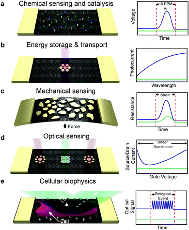 |
| | Fig. 1 Overview of the phenomena and applications of metallic nanoislands on graphene. Applications are shown for nanoisland–graphene composites with various types of metals and morphologies on graphene, shown schematically in the left-land column. The right-hand column shows idealized comparisons of the signals produced by bare graphene (green lines) versus graphene covered with metallic nanoislands (blue lines). (a) Applications in chemistry include sensing of hydrogen gas using palladium nanoisland–graphene composites. Hydrogen gas dimers are shown in green and chemisorbed dimers are shown in blue. (b) Applications in energy conversion and storage include lithographically patterned gold on graphene for photocurrent generation. (c) Mechanical applications include the detection of strain using changes in the resistance in gold nanoislands supported by graphene. (d) Optical applications include the use of precisely patterned gold nanoislands supported by graphene for optically doping graphene, e.g., to make light-activated p–n junctions. (e) Applications in biology include the optical detection of biological events, such as cell contractions. | |
Fabrication strategies
Chemical synthesis
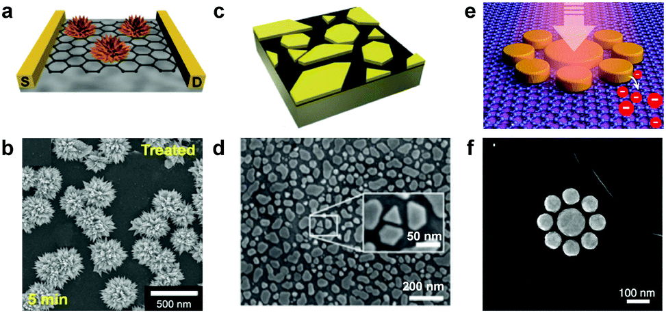
Metallic nanoislands can be deposited on graphene directly using solution-phase synthesis.14–18 Crystallites of metal nucleate and grow directly on the surface of graphene, enabling the controlled growth of single crystals of metal and even complex geometries such as spheres,19 rods,20,21 or flower-like nanoparticles (Fig. 2a).15 While a wet chemical method allows some degree of control of the shapes of nanoparticles, along with the crystalline quality (Fig. 2b), it also results in an uncontrolled distribution of metal on the surface of graphene. A random distribution of particles may not have deleterious effects on applications such as catalysis, but limits other applications (i.e., electronics and photonics) that require deterministic placement of nanoparticles.
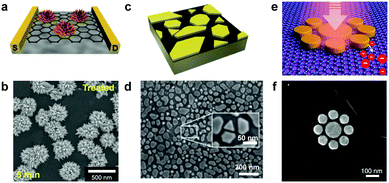 |
| | Fig. 2 Examples of metallic nanoislands on graphene deposited from solution, vapour, or patterned lithographically. (a) Schematic drawing and (b) scanning electron micrograph of palladium nanoflowers on graphene fabricated using a wet chemical method. Reprinted with permission from ref. 15. Copyright © 2015, Nature Publishing Group. (c) Schematic drawing and (d) micrograph of gold nanoislands on graphene fabricated using PVD. Reprinted with permission from ref. 6. Copyright © 2016, American Chemical Society. (e) A drawing and (f) a micrograph of radially symmetric gold discs patterned on graphene for photonic applications. Reprinted with permission from ref. 26 Copyright © 2012, American Chemical Society. | |
Physical vapor deposition
Physical vapor deposition (PVD) of metal, such as by electron-beam or thermal evaporation, produces disconnected nanoislands at low nominal thicknesses (Fig. 2c). While the shapes of the nanoparticles produced by this method are not deterministic, some degree of control can be achieved by tuning the parameters of deposition. For example, the evaporation rate and substrate temperature can be used to control the crystallinity, size distribution, and interconnectivity of the nanoislands.22 The unique surface properties of graphene provide an additional mechanism to control the morphology of the nanoislands during deposition. Rafiee and coworkers first observed that the surface energy of the substrate supporting the graphene can influence the surface energy of the graphene—an effect known as “wetting transparency”.23,24 This phenomenon can be leveraged to control the nanoisland morphology by simply switching the substrate that is supporting the graphene during the deposition process.6 Finally, Xiang et al. reported that thermal annealing of the nanoislands after deposition can cause the nanoislands to assemble into quasi-ordered arrays.25 While limited in precision, tuning parameters in PVD and post-processing provides a simple method to control the morphology of metallic nanoislands on graphene.
Lithography
Electron-beam lithography (EBL) and photolithography offer the ability to produce deterministic patterns of metal on single-layer graphene.26,27 These methods can produce patterns with controllable periodicity and geometry, which are critical parameters in plasmonics,28 light scattering,29 and quantum tunneling.30,31 Particularly, optical sensing platforms, like SERS, benefit greatly from the precision of lithographic techniques due to the dependence of signal sensitivity on nanoparticle spacing. EBL has been used for fabrication of radially symmetric metal nanostructures on graphene with sub-micron features (Fig. 2e and f). Lithographic methods, while affording deterministic control over the geometries of the nanoislands, can do so only over small areas, and scale-up may be problematic for some applications.
Chemical applications
Gas sensing
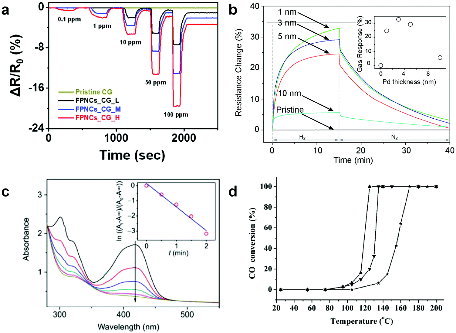
Metallic nanoislands on graphene have been used as sensors for a variety of gases such as hydrogen,32,33 NOx species,21 and ethanol vapor.34 In these applications, the graphene acts as an inert, flexible, and conductive substrate for the metal, which undergoes a physicochemical interaction with the gas species of interest. Changes in the resistivity in the nanoisland–graphene composite as the gas interacts with the metal can be measured. For example, Shin and coworkers demonstrated the use of palladium flower-like nanoparticles supported by graphene for hydrogen sensing as shown in Fig. 3a. In this example, the shapes of the nanoparticles and sensitivities to gases were determined by the growth time of the nanoparticles.15 The sensitivity of these nanoisland–graphene composites is determined by nanoparticle surface area, which limits the chemical kinetics. Shorter reaction times lead to smaller particles with a higher surface area to volume ratio. This higher ratio increases the total amount of hydrogen that can chemisorb to the surface and thus increases the sensitivity. This trend with particle size and sensitivity has also been observed for simpler geometries such as palladium spheres on graphene (Fig. 3b).35 In addition to metals, semiconductor nanoparticles, such as oxides of tin, copper, and zinc, supported by graphene, have also been used for hydrogen sensors with lower detection limits at higher temperatures than their metal counterparts.36
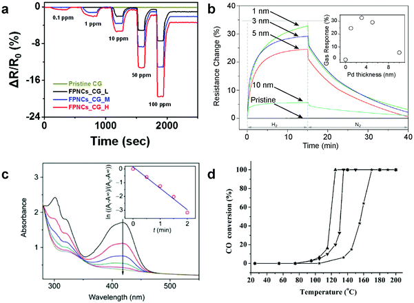 |
| | Fig. 3 Chemical applications for metallic nanoislands on graphene. (a) Hydrogen gas sensing performance is depicted for palladium nanoflowers (reprinted with permission from ref. 15. Copyright © 2015, Nature Publishing Group) and (b) nanoislands (Reprinted with permission from ref. 35. Copyright © 2012, Elsevier) supported by graphene. (c) Time-dependent UV-vis spectra of a solution containing silver nanoislands supported by graphene shows the performance as a catalyst for reduction of hexacyanoferrate(III) by sodium borohydride Reprinted with permission from ref. 5. Copyright © 2011, Science China Press and Springer-Verlag Berlin Heidelberg. The arrow in (c) points in the direction of increasing time. (d) Catalytic performance (by percent conversion of CO) of platinum nanoparticles supported by reduced-graphene oxide (Pt-rGO) at various temperatures is shown. Reprinted with permission from ref. 40. Copyright © 2014, Wiley-VCH Verlag, GmbH & Co. KGaA. The effect of calcination at 500 °C (▼) and 700 °C (▲) on Pt-rGO substrates is also shown in (d) as well as a sample without calcination (★) as a control. | |
Catalysis
The high ratio of surface area to volume of metal nanoislands on graphene makes them useful substrates for catalysis.37,38 For this application, the graphene acts as an inert support for the metal catalyst. The flexibility of graphene allows it to adhere conformably to a surface of interest, or fold and wrinkle, increasing the active catalytic area per unit volume. While this is a common technique for designing catalyst supports, most supports are rigid ceramics, whereas graphene is flexible.39 Examples of metal nanoislands for liquid-phase catalyst applications includes the use of silver, platinum, palladium, and gold nanoislands supported on graphene for the catalysis of redox reactions (Fig. 3c).5 Examples of catalysis applications include the use of graphene-supported platinum nanoislands for carbon monoxide conversion and liquid-phase high temperature catalysis (Fig. 3d).40 Catalytic applications of graphene composites, in particular, are described in detail by many recent reviews.41–43
Mechanical sensing
Metallic nanoislands on graphene exhibit an exceptional degree of piezoresistance—a change in electrical resistance with mechanical strain. Graphene44–46 and metal47 are both intrinsically piezoresistive. For metals, this effect is predominately geometrical; there is a negligible change in the resistivity with strain. For graphene, however, mechanical strain also induces a significant increase in the resistivity. This effect has been shown to result from a reduction in the electron mobility with strain.48 When metallic nanoislands are deposited by vapor deposition on graphene, the graphene acts as a conductive, stretchable, flexible and strengthening support.49,50 Under small strains (less than approximately 1%), the conductivity is mediated, in part, by the tunneling of electrons across gaps between the metal nanoparticles. In principle, this modality permits a high degree of piezoresistance because tunneling current is exponentially dependent on the distance between the nanoislands.51 Recently, our group investigated the piezoresistance of gold and palladium nanoislands on graphene. Gauge factors, defined as the ratio of the relative change in electrical resistance to the mechanical strain, were measured to be over 100 in the small strain regime. This sensitivity is an order of magnitude better than conventional thin-film metal strain gauges. The reproducible dynamic behavior also spanned a wide range (0.001–9% strain), a useful trait for strain sensors. Usually, strain sensors excel in sensitivity but are limited in dynamic range or vice versa. Moreover, gold nanoislands have proven to be compatible with biological cells, such as mammalian cardiomyocytes (Fig. 4a). The increased sensitivity by electron-tunneling in gold nanoisland substrates permits the detection of microscale deformations induced by the contractions of these cells (Fig. 4b).6 Additionally, larger strains are detectable (>1%) owing to the stretchable, underlying graphene which permits sensing of larger-scale deformations such as the pulse in the radial artery for wearable physiological sensors using gold nanoislands (Fig. 4c). Finally, silver nanoisland–graphene composites have been used for other wearable applications, including speech detection (Fig. 4d) and bending of fingers (Fig. 4e).52
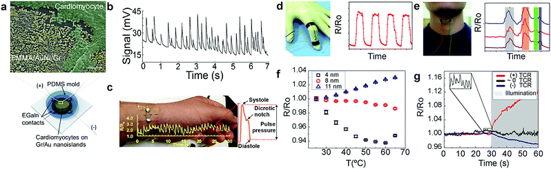 |
| | Fig. 4 Mechanical sensing with metal nanoisland–graphene composites. Metal nanoisland–graphene composites have been used for a variety of strain sensors based on piezoresistivity. (a) Gold nanoislands on graphene (AuNI–Gr) have been shown to be biocompatible substrates for mammalian cardiomyocytes as shown by false-colored SEM micrographs (scale bar 200 nm). A schematic of the sensing platform is also shown in (a). (b) Additionally, AuNI–Gr substrates have been used for the piezoresistive detection of mammalian cardiomyocyte cell contractions through voltage measurements. (c) Wearable strain sensors such as palladium nanoislands supported on graphene have been used for measurement of human pulse using changes in resistivity. (a–c) Reprinted with permission from ref. 6. Copyright © 2016, American Chemical Society. Other wearable applications using resistivity changes include the use of graphene–silver nanoparticle networks for the detection of finger contractions (d) and the detection of throat contractions induced by speech (e). The phrase “Hi, how are you” is shown in (e) for three separate human subjects, which show similar waveforms. (d and e) Reprinted with permission from ref. 52 and the Royal Society of Chemistry. The resistance of a AuNI–Gr substrate can vary with temperature and cause unwanted thermal drift. (f) The dependence of resistance on temperature, or the thermal coefficient of resistance (TCR), can be controlled by varying the amount of gold deposited on graphene. Controlling the TCR minimizes thermal drift in wearable sensors as depicted in (g) which shows the thermal drift for three sensors after being heated by a solar simulator lamp. (f and g) Reprinted with permission from ref. 54. Copyright © 2017, American Chemical Society. | |
In all the examples discussed, detection of mechanical deformation relies on a piezoresistive effect. However, if the thermal coefficient of resistance (TCR) is large, then temperature fluctuations will also cause changes in the resistivity that are comparable to the changes due to strain (i.e., thermal drift).53 Noting that the TCR of metals is positive and that of graphene is negative, we reasoned that it should be possible to tune the amount of metal to achieve a near-zero TCR. Using this strategy, we were able to minimize thermal drift in metal nanoisland–graphene composites by controlling the surface coverage of metal in the composite (Fig. 4f).54 This design strategy enabled the fabrication of a wearable sensor that exhibited stability against abrupt and large temperature fluctuations such as exposure to simulated sunlight (Fig. 4g). Critically, this strategy used control of the materials—as opposed to backend electronics—to stabilize the signal.
Energy transport and storage
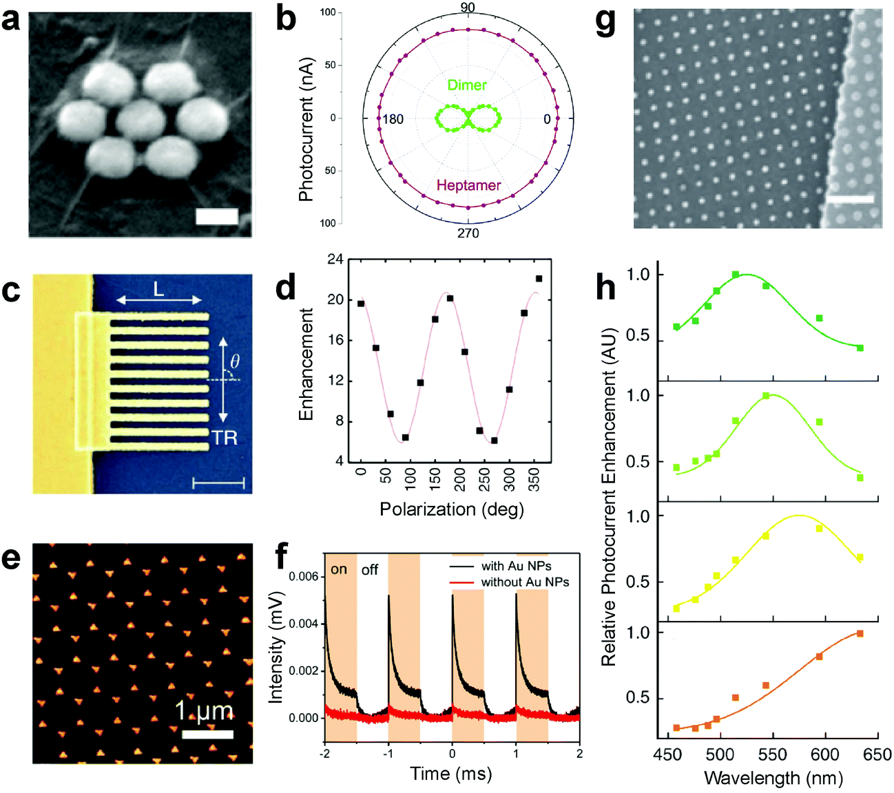
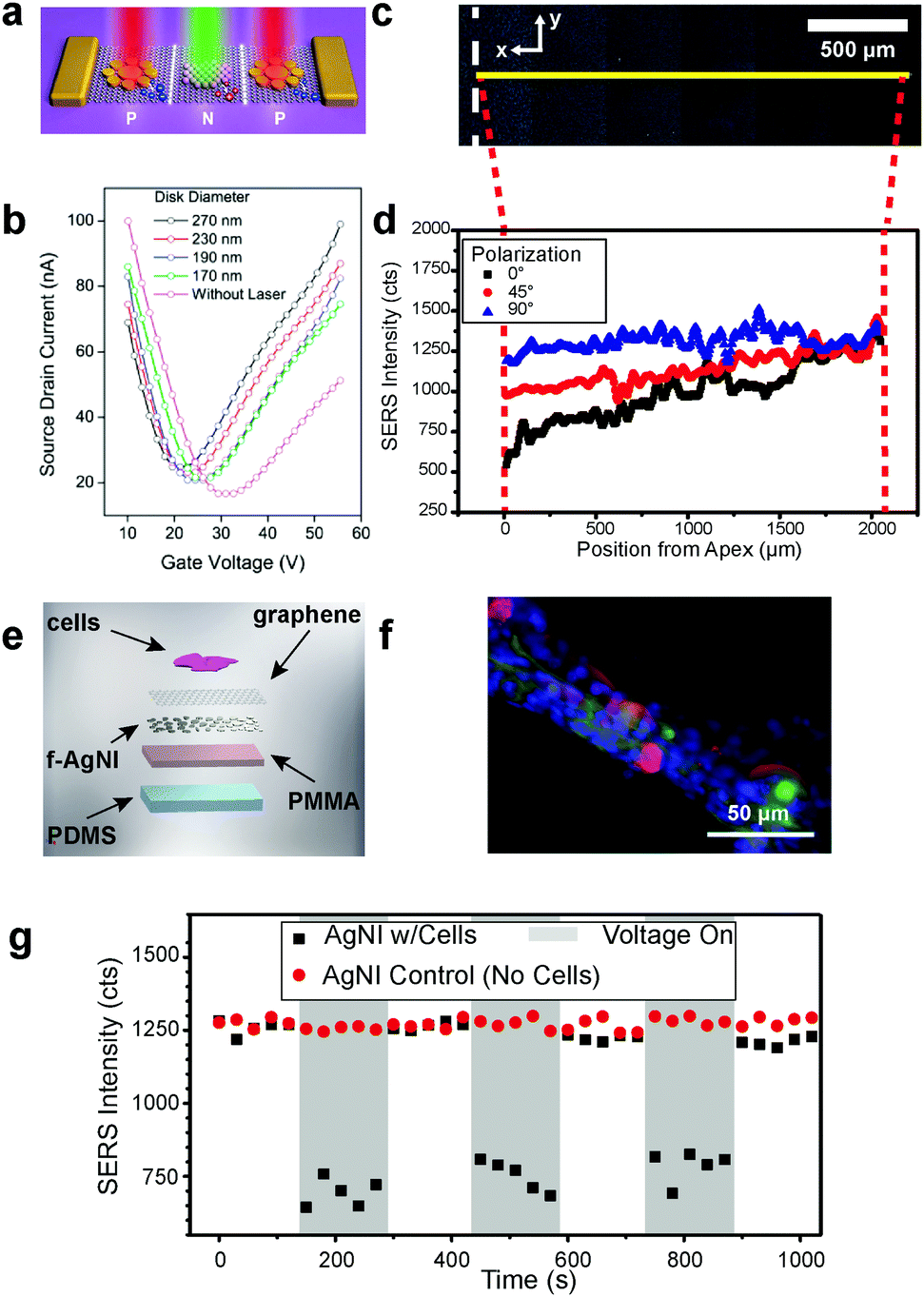
A wide variety of metals have been explored in metal nanoisland–graphene composites for fuel cell applications.2,55–61 This topic has been reviewed in detail by Liu and coworkers.62 Additionally, other two-dimensional materials, such as tungsten disulfide and molybdenum disulfide, have been used for hydrogen evolution in fuel cells.63 Metal nanoparticles on graphene have also been used as co-catalysts for hydrogen evolution by photocatalytic water splitting, while maintaining separation of charge carriers for the generation of energy.64,65 In all these cases, graphene acts as a functional material and a flexible substrate. The choice of metal can significantly improve the efficiency of fuel cells.66 Other applications in energy conversion include the use of symmetric patterns of gold on graphene for the generation of photocurrent by Halas and others.3,27,67–71 In these applications, the gold is used to enhance light absorption by localized surface plasmon resonance, and hot carriers are shuttled into the underlying graphene which generates a photocurrent. Radial symmetry of the gold structures is crucial in this application, as it mitigates phonon scattering, which impedes electron transport. In work by Fang et al., polarization dependent photocurrent was demonstrated using dimer and heptamer gold structures on graphene (Fig. 5a and b). Similar work exploiting surface plasmon resonance was demonstrated by Etchermeyer and coworkers who showed significant polarization-dependent enhancement of photocurrent with simple patterns of gold lines (Fig. 5c and d).69 Radially symmetric structures, such as gold bowtie antennas fabricated by nanosphere lithography fabricated by Chen and coworkers,67 have been used to enhance light absorption in the NIR and enhanced photoresponse (Fig. 5e and f). The strong wavelength dependence of surface plasmon resonance on geometry allows researchers to adjust parameters lithographically, such as the spacing of nanodisks by Liu and coworkers (Fig. 5g), and subsequently control the wavelength of light absorbed (Fig. 5h).3 Nam and coworkers have exploited buckling as a method to tune the dispersion and sensitivity of nanoisland–graphene photodetectors.72 In all of these cases, the graphene plays a crucial role in electronic transport while the metal nanostructures aid in enhancing light absorption and subsequent generation of photocarriers.
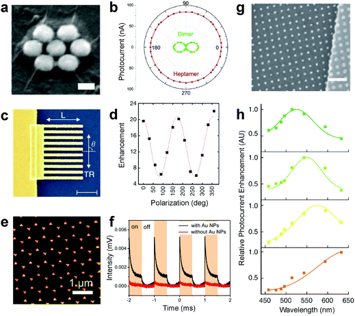 |
| | Fig. 5 Applications for metal nanoisland–graphene composites in energy storage and transport. (a) An SEM micrograph shows gold–graphene sandwiches used for polarization-dependent generation of photocurrent (scale bar 40 nm). (b) The photocurrent of graphene is controlled using the geometry of the gold nanoparticle patterns and polarization is depicted. (a and b) Reprinted with permission from ref. 27. Copyright 2012, American Chemical Society. (c) An SEM micrograph of lithographically patterned gold nanowires (AuNW) on graphene is shown (scale bar 1 μm). (d) The polarization dependent plasmon enhancement of photocurrent in graphene due to AuNWs is shown. (c and d) Reprinted with permission from ref. 69. Copyright 2011, Nature Publishing Group. (e) Nanosphere lithography has been used to fabricate gold bowtie antennae on graphene (AuBT–Gr) as shown by SEM micrograph. (f) AuBT–Gr substrates have exhibited a highly sensitive time response for photocurrent as shown in (f), which shows great promise in photodetector applications. (e and f) Reprinted with permission from ref. 67. Copyright 2017, American Chemical Society. (g) An SEM micrograph shows cubic lattices of gold nanoislands can patterned on graphene with superlative control of spacing (scale bar 400 nm). (h) Control of the spacing in gold nanoparticle patterns allows for the tuning of photocurrent enhancement over a wide variety of wavelengths, as depicted by the absorption spectra in (h). (g and h) Reprinted with permission from ref. 3. Copyright 2011, Nature Publishing Group. The nanoparticle spacing in (h) is 18 nm (green), 50 nm (orange), 100 nm (yellow) and 400 nm (red). | |
Optical applications
For metallic nanoislands on graphene in optical applications, the role of graphene has varied from substrate to functional material. For example, Fang and coworkers have used precisely patterned gold nanostructures on graphene (Fig. 6a) for optically doped p–n junctions, where the spacing of particles determines both the wavelength of light absorbed and nature of the photocarrier injected into the underlying graphene.26 The result is a composite material that exhibits semiconducting behavior that can be modulated by the wavelength of illuminating light (Fig. 6b). Interestingly, the graphene assumes a role of semiconductor and substrate, analogous to silicon in traditional p–n junctions. Metasurfaces comprising patterned gold resonators on graphene have also been used as gate-tunable, reflective phase modulators for mid-infrared beam steering.73 Another optical application that has seen considerable attention is the use of metal nanoisland–graphene composites as substrates for surface-enhanced Raman scattering (SERS).6,25,74–78 The role of graphene in the majority of these applications is as a substrate, allowing easy transfer onto arbitrary substrates for specific applications such as optical strain sensing using SERS (Fig. 6c and d).7 Additionally, it has been shown that graphene can also mitigate the effects of fluorescence in SERS signal-to-noise ratios. In recent work, the role of graphene has been expanded by exploiting its electrical conductivity to actuate musculoskeletal cells (Fig. 6e and f). This approach permitted the simultaneous electrical stimulation and optical detection (Fig. 6g) of musculoskeletal contractions, providing orthogonal modes of interrogation and sensing.
 |
| | Fig. 6 Optical applications of metal nanoisland–graphene composites. (a) Use of the composition and geometric pattern of metal to selectively dope the underlying graphene with incident light, using localized surface plasmons. Further modification of individual nanoparticle geometries allows additional control over the electron transport properties (b). (a and b) Reprinted with permission from ref. 26. Copyright © 2012, American Chemical Society. Metal nanoislands on graphene have been used extensively as surface-enhanced Raman scattering (SERS) substrates with numerous applications such as structural strain mapping and time-dependent biological strain detection (c–g). (c–g) Reprinted and adapted with permission from ref. 7 and the Royal Society of Chemistry. Silver nanoislands supported by graphene on a bent glass substrate is depicted (c) with the SERS mapped area marked by the narrow yellow box and the apex of the bent glass marked by the white dashed line. The strain gradient of the bent glass is detectable by SERS intensity attenuation (d), which results from nanoislands being pulled apart; polarization angle provides additional data on the direction of strain. Silver nanoisland on graphene substrates have been used for the simultaneous stimulation and detection of musculoskeletal cell (C2C12 myoblast) contractions through SERS (e). A fluorescence image of C2C12 cells on the silver nanoisland substrate is depicted (f) with nuclei (blue), actin (green), and myosin heavy chain (red) shown. Cell contractions were stimulated by applying a voltage across the conductive silver nanoisland substrate and detected using attenuations in the SERS signal (g). | |
Conclusions
This minireview has discussed a versatile class of composite material comprising metallic nanoislands on graphene. While made of conductive components, the nanoscale arrangement of disconnected nanoislands on a graphene surface gives rise to properties that can be modulated in ways reminiscent of semiconductors. The unique properties of this composite material have led to a wide variety of applications. Applications in chemistry include the use of metal nanoisland–graphene composites for thin-film catalysts with remarkable efficiency. Applications in mechanical sensing include the use of nanoislands for wearable sensors for gesture recognition and cardiac health monitoring. Applications in biological sensing include the use of both optical (piezoplasmonic) and electronic (piezoresistive) modalities for the detection of cellular activity such as mammalian cardiomyocyte and stimulated-myoblast contractions. Both optical and electronic modalities have demonstrated high gauge factors in this area of cellular strain sensing. The field of energy storage and energy transport has employed nanoislands as a catalyst for conversion in fuel cells and highly efficient photodetectors. In summary, the range of application for this simple, two-component metamaterial is extensive. Future work will most likely broaden it even further, as various methods of fabrication make this metamaterial easily attainable. From a materials development perspective, there is a tremendous amount of work left to be done to understand the fundamentals behind the optical, electronic, and mechanical properties that result from a physicochemical interface between graphene and metal nanoislands. A clearer understanding of new properties may be accomplished by first-principle electromagnetic or mechanical simulations of graphene-metal composites. A fundamental understanding of the origin, limits, and utility of these emergent properties will lead to effective engineering of metal nanoisland–graphene composites in the future.
Conflicts of interest
There are no conflicts to declare.
Acknowledgements
This work was supported by the National Institutes of Health Director's New Innovator Award, grant 1DP2EB022358-01 and by a Diversity Supplement (for B. C. M.) under the same award number.
References
- S. M. Choi, S. H. Jhi and Y. W. Son, Nano Lett., 2010, 10, 3486–3489 CrossRef CAS PubMed.
- C. Xu, X. Wang and J. Zhu, J. Phys. Chem. C, 2008, 112, 19841–19845 CAS.
- Y. Liu, R. Cheng, L. Liao, H. Zhou, J. Bai, G. Liu, L. Liu, Y. Huang and X. Duan, Nat. Commun., 2011, 2, 579 CrossRef PubMed.
- P. Kang, M. C. Wang, P. M. Knapp and S. W. Nam, Adv. Mater., 2016, 28, 4565 CrossRef.
- H. He and C. Gao, Sci. China: Chem., 2011, 54, 397–404 CrossRef CAS.
- A. V. Zaretski, S. E. Root, A. Savchenko, E. Molokanova, A. D. Printz, L. Jibril, G. Arya, M. Mercola and D. J. Lipomi, Nano Lett., 2016, 16, 1375–1380 CrossRef CAS PubMed.
- B. C. Marin, J. Liu, E. Aklile, A. D. Urbina, A. S. Chiang, N. Lawrence, S. Chen and D. J. Lipomi, Nanoscale, 2016, 9, 1292–1298 RSC.
- P. V. Kamat, J. Phys. Chem. Lett., 2010, 1, 520–527 CrossRef CAS.
- V. Georgakilas, M. Otyepka, A. B. Bourlinos, V. Chandra, N. Kim, K. C. Kemp, P. Hobza, R. Zboril and K. S. Kim, Chem. Rev., 2012, 112, 6156–6214 CrossRef CAS PubMed.
- A. Reina, H. Son, L. Jiao, B. Fan, M. S. Dresselhaus, Z. Liu and J. Kong, J. Phys. Chem. C, 2008, 112, 17741–17744 CAS.
- S. Bae, H. Kim, Y. Lee, X. Xu, J.-S. Park, Y. Zheng, J. Balakrishnan, T. Lei, H. Ri Kim, Y. Il Song, Y.-J. Kim, K. S. Kim, B. Özyilmaz, J.-H. Ahn, B. H. Hong and S. Iijima, Nat. Nanotechnol., 2010, 5, 574–578 CrossRef CAS PubMed.
- A. Reina, X. Jia, J. Ho, D. Nezich, H. Son, V. Bulovic, M. S. Dresselhaus, J. Kong, K. S. K. S. Kim, Y. Zhao, H. Jang, S. Y. Lee, J. M. Kim, J.-H. Ahn, P. Kim, J.-Y. Choi and B. H. Hong, Nano Lett., 2009, 9, 30–35 CrossRef CAS PubMed.
- L. G. De Arco, Y. Zhang and C. Schlenker, ACS Nano, 2010, 4, 2865–2873 CrossRef PubMed.
- W. Hong, H. Bai, Y. Xu, Z. Yao, Z. Gu and G. Shi, J. Phys. Chem. C, 2010, 114, 1822–1826 CAS.
- D. H. Shin, J. S. Lee, J. Jun, J. H. An, S. G. Kim, K. H. Cho and J. Jang, Sci. Rep., 2015, 5, 1–11 Search PubMed.
- X. Zhou, X. Huang, X. Qi, S. Wu, C. Xue, F. Y. C. Boey, Q. Yan, P. Chen and H. Zhang, J. Phys. Chem. C, 2009, 113, 10842–10846 CAS.
- X. Chen, G. Wu, J. Chen, X. Chen, Z. Xie and X. Wang, J. Am. Chem. Soc., 2011, 133, 3693–3695 CrossRef CAS PubMed.
- Y. C. Wan, H. F. Teoh, E. S. Tok and C. H. Sow, J. Appl. Phys., 2015, 117, 1–9 Search PubMed.
- R. Muszynski, B. Seger and P. V. Kamat, J. Phys. Chem. C, 2008, 112, 5263–5266 CAS.
- J. W. Lee, A. S. Hall, J. D. Kim and T. E. Mallouk, Chem. Mater., 2012, 24, 1158–1164 CrossRef CAS.
- X. An, J. C. Yu, Y. Wang, Y. Hu, X. Yu and G. Zhang, J. Mater. Chem., 2012, 22, 8525 RSC.
- T. T. Tsong, Prog. Surf. Sci., 2003, 74, 69–80 CrossRef CAS.
- J. Rafiee, X. Mi, H. Gullapalli, A. V. Thomas, F. Yavari, Y. Shi, P. M. Ajayan and N. A. Koratkar, Nat. Mater., 2012, 11, 217–222 CrossRef CAS PubMed.
- S. Chae, S. Jang, W. J. Choi, Y. S. Kim, H. Chang, T. Il Lee and J.-O. Lee, Nano Lett., 2017, 17, 1711–1718 CrossRef CAS PubMed.
- Q. Xiang, X. Zhu, Y. Chen and H. Duan, Nanotechnology, 2016, 27, 75201 CrossRef PubMed.
- Z. Fang, Y. Wang, Z. Liu, A. Schlather, P. M. Ajayan, F. H. L. Koppens, P. Nordlander and N. J. Halas, ACS Nano, 2012, 6, 10222–10228 CrossRef CAS PubMed.
- Z. Fang, Z. Liu, Y. Wang, P. M. Ajayan, P. Nordlander and N. J. Halas, Nano Lett., 2012, 12, 3808–3813 CrossRef CAS PubMed.
- S. K. Ghosh and T. Pal, Chem. Rev., 2007, 107, 4797–4862 CrossRef CAS PubMed.
- D. P. Fromm, A. Sundaramurthy, P. James Schuck, G. Kino and W. E. Moerner, Nano Lett., 2004, 4, 957–961 CrossRef CAS.
- J. A. Scholl, A. García-Etxarri, A. L. Koh and J. A. Dionne, Nano Lett., 2013, 13, 564–569 CrossRef CAS PubMed.
- R. B. Laughlin, Phys. Rev. B: Condens. Matter Mater. Phys., 1981, 23, 5632–5633 CrossRef.
- J. Yi, S. H. Kim, W. W. Lee, S. S. Kwon, S. W. Nam and W. I. Park, J. Phys. D: Appl. Phys., 2015, 48, 475103 CrossRef.
- W. Wu, Z. Liu, L. A. Jauregui, Q. Yu, R. Pillai, H. Cao, J. Bao, Y. P. Chen and S. S. Pei, Sens. Actuators, B, 2010, 150, 296–300 CrossRef CAS.
- J. Yi, J. M. Lee and W. I. Park, Sens. Actuators, B, 2011, 155, 264–269 CrossRef CAS.
- M. G. Chung, D. H. Kim, D. K. Seo, T. Kim, H. U. Im, H. M. Lee, J. B. Yoo, S. H. Hong, T. J. Kang and Y. H. Kim, Sens. Actuators, B, 2012, 169, 387–392 CrossRef CAS.
- Z. Zhang, X. Zou, L. Xu, L. Liao, W. Liu, J. Ho, X. Xiao and C. Jiang, Nanoscale, 2015, 7, 10078–10084 RSC.
- S. Navalon, A. Dhakshinamoorthy, M. Alvaro and H. Garcia, Coord. Chem. Rev., 2016, 312, 99–148 CrossRef CAS.
- L. Hang, Y. Zhao, H. Zhang, G. Liu, W. Cai, Y. Li and L. Qu, Acta Mater., 2016, 105, 59–67 CrossRef CAS.
- N. M. Julkapli and S. Bagheri, Int. J. Hydrogen Energy, 2015, 40, 948–979 CrossRef CAS.
- L. Shang, T. Bian, B. Zhang, D. Zhang, L. Z. Wu, C. H. Tung, Y. Yin and T. Zhang, Angew. Chem., Int. Ed., 2014, 53, 250–254 CrossRef CAS PubMed.
- C. Huang, C. Li and G. Shi, Energy Environ. Sci., 2012, 5, 8848 CAS.
- Y. Liu, X. Dong and P. Chen, Chem. Soc. Rev., 2012, 41, 2283–2307 RSC.
- X. Zhou, J. Qiao, L. Yang and J. Zhang, Adv. Energy Mater., 2014, 4, 1–25 Search PubMed.
- C. Yan, J. Wang, W. Kang, M. Cui, X. Wang, C. Y. Foo, K. J. Chee and P. S. Lee, Adv. Mater., 2014, 26, 2022–2027 CrossRef CAS PubMed.
- M. Kumar and H. Bhaskaran, Nano Lett., 2015, 15, 2562–2567 CrossRef CAS PubMed.
- M. Tsui and M. F. Islam, Nanoscale, 2016, 1128–1135 Search PubMed.
- M. Li, H. X. Tang and M. L. Roukes, Nat. Nanotechnol., 2007, 2, 114–120 CrossRef CAS PubMed.
- A. D. Smith, F. Niklaus, A. Paussa, S. Vaziri, A. C. Fischer, M. Sterner, F. Forsberg, A. Delin, D. Esseni, P. Palestri, M. Östling and M. C. Lemme, Nano Lett., 2013, 13, 3237–3242 CrossRef CAS PubMed.
- A. D. Smith, F. Niklaus, A. Paussa, S. Schroder, A. C. Fischer, M. Sterner, S. Wagner, S. Vaziri, F. Forsberg, D. Esseni, M. Ostling and M. C. Lemme, ACS Nano, 2016, 10, 9879–9886 CrossRef CAS PubMed.
- Y. Kim, J. Lee, M. S. Yeom, J. W. Shin, H. Kim, Y. Cui, J. W. Kysar, J. Hone, Y. Jung, S. Jeon and S. M. Han, Nat. Commun., 2013, 4, 2114 Search PubMed.
- L. Yi, W. Jiao, K. Wu, L. Qian, X. Yu, Q. Xia, K. Mao, S. Yuan, S. Wang and Y. Jiang, Nano Res., 2015, 8, 2978–2987 CrossRef CAS.
- S. Chen, Y. Wei, X. Yuan, Y. Lin and L. Liu, J. Mater. Chem. C, 2016, 4, 4304–4311 RSC.
- P. Sun, M. Zhu, K. Wang, M. Zhong, J. Wei, D. Wu and H. Zhu, ACS Appl. Mater. Interfaces, 2013, 5, 9563–9571 CAS.
- B. C. Marin, S. E. Root, A. D. Urbina, E. Aklile, R. Miller, A. V. Zaretski and D. J. Lipomi, ACS Omega, 2017, 2, 626–630 CrossRef CAS PubMed.
- Y. Liang, H. Wang, J. Zhou, Y. Li, J. Wang, T. Regier and H. Dai, J. Am. Chem. Soc., 2012, 134, 3517–3523 CrossRef CAS PubMed.
- Y. Qian, C. Wang and Z.-G. Le, Appl. Surf. Sci., 2011, 257, 10758–10762 CrossRef CAS.
- Y. Li, W. Gao, L. Ci, C. Wang and P. M. Ajayan, Carbon, 2010, 48, 1124–1130 CrossRef CAS.
- Y. Liang, Y. Li, H. Wang, J. Zhou, J. Wang, T. Regier and H. Dai, Nat. Mater., 2011, 10, 780–786 CrossRef CAS PubMed.
- Z. S. Wu, Y. Sun, Y. Z. Tan, S. Yang, X. Feng and K. Müllen, J. Am. Chem. Soc., 2012, 134, 19532–19535 CrossRef CAS PubMed.
- H. Wang, Y. Liang, Y. Li and H. Dai, Angew. Chem., Int. Ed., 2011, 50, 10969–10972 CrossRef CAS PubMed.
- M. Jiang, H. He, C. Huang, B. Liu, W.-J. Yi and Z.-S. Chao, Electrochim. Acta, 2016, 219, 492–501 CrossRef CAS.
- M. Liu, R. Zhang and W. Chen, Chem. Rev., 2014, 114, 5117–5160 CrossRef CAS PubMed.
- J. Kim, S. Byun, A. J. Smith, J. Yu and J. Huang, J. Phys. Chem. Lett., 2017, 4, 1227–1232 CrossRef PubMed.
- G. P. Singh, K. M. Shrestha, A. Nepal, K. J. Klabunde and C. M. Sorensen, Nanotechnology, 2014, 25, 265701 CrossRef CAS PubMed.
- G. Xie, K. Zhang, B. Guo, Q. Liu, L. Fang and J. R. Gong, Adv. Mater., 2013, 25, 3820–3839 CrossRef CAS PubMed.
- L. Dong, R. R. S. Gari, Z. Li, M. M. Craig and S. Hou, Carbon, 2010, 48, 781–787 CrossRef CAS.
- Z. Chen, X. Li, J. Wang, L. Tao, M. Long, S.-J. Liang, L. K. Ang, C. Shu, H. K. Tsang and J.-B. Xu, ACS Nano, 2017 DOI:10.1021/acsnano.6b06172.
- T. J. Echtermeyer, S. Milana, U. Sassi, A. Eiden, M. Wu, E. Lidorikis and A. C. Ferrari, Nano Lett., 2016, 16, 8–20 CrossRef CAS PubMed.
- T. J. Echtermeyer, L. Britnell, P. K. Jasnos, A. Lombardo, R. V. Gorbachev, A. N. Grigorenko, A. K. Geim, A. C. Ferrari and K. S. Novoselov, Nat. Commun., 2011, 2, 458 CrossRef CAS PubMed.
- Y. L. Liu, C. C. Yu, K. Te Lin, T. C. Yang, E. Y. Wang, H. L. Chen, L. C. Chen and K. H. Chen, ACS Nano, 2015, 9, 5093–5103 CrossRef CAS PubMed.
- R. Maiti, T. K. Sinha, S. Mukherjee, B. Adhikari and S. K. Ray, Plasmonics, 2016, 11, 1297–1304 CrossRef CAS.
- M. Kim, P. Kang, J. Leem and S. Nam, Nanoscale, 2017, 23–27 Search PubMed.
- M. C. Sherrott, P. W. C. Hon, K. T. Fountaine, J. C. Garcia, S. M. Ponti, V. W. Brar, L. A. Sweatlock and H. A. Atwater, Nano Lett., 2017, 17, 3027–3034 CrossRef CAS PubMed.
- L.-W. Nien, M.-H. Chien, B.-K. Chao, M.-J. Chen, J.-H. Li and C.-H. Hsueh, J. Phys. Chem. C, 2016, 120, 3448–3457 CAS.
- J. Leem, M. C. Wang, P. Kang and S. Nam, Nano Lett., 2015, 15, 7684–7690 CrossRef CAS PubMed.
- I. Khalil, N. M. Julkapli, W. A. Yehye, W. J. Basirun and S. K. Bhargava, Materials, 2016, 9, 406 CrossRef PubMed.
- W. Hu, Z. Huang, Y. Zhou, W. Cai and J. Kang, Sci. China: Phys., Mech. Astron., 2014, 57, 2021–2023 CrossRef CAS.
- C. Yang, C. Zhang, Y. Huo, S. Jiang, H. Qiu, Y. Xu, X. Li and B. Man, Carbon, 2016, 98, 526–533 CrossRef CAS.
|
| This journal is © The Royal Society of Chemistry 2017 |

 *
*