
 Open Access Article
 This Open Access Article is licensed under a Creative Commons Attribution-Non Commercial 3.0 Unported Licence
N-type polymers as electron extraction layers in hybrid perovskite solar cells with improved ambient stability†
S.
Shao
a,
Z.
Chen
b,
H.-H.
Fang
 a,
G. H.
ten Brink
a,
D.
Bartesaghi
a,
S.
Adjokatse
a,
L. J. A.
Koster
a,
B. J.
Kooi
a,
A.
Facchetti
b and
M. A.
Loi
*a
a,
G. H.
ten Brink
a,
D.
Bartesaghi
a,
S.
Adjokatse
a,
L. J. A.
Koster
a,
B. J.
Kooi
a,
A.
Facchetti
b and
M. A.
Loi
*a
aZernike Institute for Advanced Materials, University of Groningen, Nijenborgh 4, 9747 AG, Groningen, The Netherlands. E-mail: m.a.loi@rug.nl
bPolyera Corporation, 8045 Lamon Avenue, Skokie, Illinois 60077, USA
First published on 15th January 2016
Abstract
We studied three n-type polymers of the naphthalenediimide-bithiophene family as electron extraction layers (EELs) in hybrid perovskite solar cells. The recombination mechanism in these devices is found to be heavily influenced by the EEL transport properties. The maximum efficiency of the devices using the n-type polymers EELs did not exceed substantially that of the devices using PC60BM (about 11%), while a substantial improvement in their ambient stability (87% of the initial value after 270 minutes) compared to that using PC60BM (3.5% of the initial value after 270 minutes) was detected.
Hybrid perovskites (HPs) are compounds with an ABX3 perovskite structure, where A is an organic cation (CH(NH2)2+ or CH3NH3+), B is a metal cation (Pb2+ or Sn2+) and X is a halide anion (Cl−, Br− and I−).1–3 These perovskite materials have ideal properties for photovoltaics, including high absorption coefficients (>104 cm−1 at 550 nm),4,5 tuneable bandgaps (from 1.1 to 2.3 eV by altering their composition),6,7 balanced charge transport and long carrier diffusion lengths (around 100 nm in CH3NH3PbI3 and 1 μm in the CH3NH3PbI3−xClx film).8–10 In addition, these materials can be processed from solution, which makes them compatible with low cost and large-scale roll-to-roll fabrication techniques. Such advantageous features have intrigued the scientific community and triggered intensive research on HPs as light absorbers in photovoltaics (PV). During the past five years, HP based solar cells (HPSCs) have witnessed a soaring increase in power conversion efficiency (PCE) from 3.8% to 20.1% through improvements in the device structure,11–15 film growth strategy,16–27 film composition,2,3 and nature of the interfacial layers.28–33 Despite such fundamental progress, challenges remain to be addressed in the development of hybrid perovskite solar cell technology. Primary among these is ensuring the stability and reproducibility of the solar cell performance and the possibility of increasing the PCE above 25%.
Since the pioneering work by Miyasaka et al., the device structure of hybrid perovskite solar cells has been revolutionized, evolving from a liquid electrolyte based architecture,11 to a solid state sensitized mesoscopic structure,12 to meso-superstructured devices, and finally to planar structures.13,14 Concurrently, the role of perovskites has evolved from a simile-dye to a semiconductor able to absorb light and to transport electrons and holes efficiently. At present, the most efficient HPSCs are based on a meso-superstructure and a planar device structure, which demonstrate comparable device performance (20.1 and 19.3%, respectively) due to the long diffusion length of electrons/holes and balanced charge transport.25,33
However, these two structures are not equivalent, both from the perspective of processing and of exploitation of hybrid perovskite solar cells. The metal oxide scaffold (TiO2 or Al2O3) used in the meso-superstructured device geometry requires high sintering temperatures (>450 °C), which are incompatible with tandem architectures and flexible substrates.13 From an economic viewpoint, the planar device structure, in which the perovskite film is sandwiched between the anode and cathode electrodes, has a clear advantage over the meso-superstructured device, due to the low processing temperatures and the simplicity of the fabrication process.
In this device configuration, in order to block the leakage current and improve charge collection, the frequently used approach is to insert electron and hole transport layers between the perovskite film and the cathode and anode electrodes, respectively. In this way, a p-i-n (regular) or n-i-p (inverted) structure is formed. The p-i-n architecture employs solution processed materials such as PEDOT:PSS for p-type transport and fullerene derivatives for n-type transport, which enables a low temperature fabrication technique compatible with flexible substrates.29
Despite the importance of the electron extraction layer (EEL), very few electron extraction materials have been studied. The fullerene derivative, known as PC60BM and commonly used as an electron acceptor in polymer solar cells (PSCs), has been proposed as an EEL in HPSCs.13,34–38 Due to the poor performance of PC60BM in extracting charges and in blocking the leakage current, several research groups have devoted efforts to modifying PC60BM by using self-assembled monolayers or coating other n-type materials on top. Such efforts have made the devices more efficient but have also made the fabrication procedure far more complicated.39–42 The limited possibility of tuning the chemical structures and the energy levels of fullerenes, along with high production cost and small solution viscosity, may limit the application of fullerenes for low cost and highly efficient HPSCs. Furthermore, PC60BM is not a good candidate for stable HPSCs due to its hydrophilicity. Therefore, non-fullerene n-type organic layers need to be explored as EELs to develop highly efficient, production economical and stable HPSCs.43,44
It has been demonstrated that n-type polymers are a good alternative candidate as electron acceptors in PSCs.45–49 Compared to PC60BM, n-type polymers give a larger possibility to tune their chemical structure and thus their energy levels to match both the light absorbing layer and the electrodes.
To date, only one paper has reported the use of an n-type polymer as an EEL in HPSCs with PCE as low as 7%.50 Therefore, still unanswered are key questions such as how the n-type polymer affects the electron extraction and collection efficiency as well as how they may influence the stability of HPSCs. As such, further investigation of the properties of the interface between perovskite films and the EEL in order to identify the desired characteristics for an n-type material for efficient and stable HPSCs is extremely relevant.
In this work we studied how the EEL influences the recombination mechanism in HPSCs by investigating the photophysical and electrical properties of the interface between perovskite films and EELs. We further investigated the effects of EELs on the ambient stability of HPSCs. The ultimate aim was to understand how to choose the EEL for efficient and ambient stable HPSCs. For this purpose, we chose a family of n-type polymers based on naphthalenediimide-bithiophene semiconducting polymers, namely, poly{[N,N′-bis(2-octyldodecyl)-naphthalene-1,4,5,8-bis(dicarboximide)-2,6-diyl]-alt-5,5′-(2,2′-bithiophene)} (P(NDI2OD-T2)), poly{[N,N′-bis(2-dodecyltetradecyl)-naphthalene-1,4,5,8-bis(dicarboximide)-2,6-diyl]-alt-5,5′-(2,2′-bithiophene)} (P(NDI2DT-T2)) and poly{[N,N′-bis(2-octyldodecyl)-1,4,5,8-naphthalenedicarboximide-2,6-diyl]-alt-5,5′-[2,2′-(1,2-ethanediyl)bithiophene]} (P(NDI2OD-TET)). The devices fabricated using P(NDI2OD-T2) and P(NDI2DT-T2) as EELs showed PCEs as high as 10.8%. In stark contrast, the devices using P(NDI2OD-TET) as an EEL showed a very low PCE of only 0.18%. Steady state and time resolved PL measurements indicated that charge extraction from the perovskite to these n-type polymers takes place efficiently despite the very small conduction band – lowest occupied molecular orbital (LUMO) offsets (max 0.12 eV) at the perovskite/polymer interface. The charge recombination mechanism seems to be affected by the nature of EEL polymers. Trap-assisted recombination was demonstrated to take place in the HPSCs fabricated with the three different polymer EELs. Bimolecular recombination in the devices using the high mobility n-type polymers P(NDI2OD-T2) and P(NDI2DT-T2) was negligible, while it was very severe in the device using the lower mobility n-type polymer P(NDI2OD-TET), due to slow charge extraction. Assuming that the barrier between the LUMO levels of the three polymers and the aluminium electrode to be similar, we attribute the variation in the device performance mainly to the discrepancy in their electron transport properties. Therefore, we conclude that the electron mobility of the EEL is the most relevant property that defines the PCE in the HPSCs with the structure used here. We further showed that HPSCs using n-type polymers as EELs show considerably enhanced stability compared to that using PC60BM as the EEL due to better protection of the HP film towards the moisture of the ambient.
Fig. 1a shows the p-i-n planar device structure used in this study, comprising ITO/PEDOT:PSS (45 nm)/CH3NH3PbI3−xClx (210 nm)/electron extraction layer (EEL, ∼30 nm)/Al (100 nm). The details of the device fabrication and characterization can be found in the ESI.† To assess the crystallinity and purity of the CH3NH3PbI3−xClx film, X-ray diffraction patterns (XRD) and absorption spectra were recorded; these are shown in Fig. S1.† The diffraction pattern displayed in Fig. S1a† shows strong and sharp peaks at 14.2° and 28.6°, which are assigned to the (110) and (220) planes of the CH3NH3PbI3−xClx, respectively. The peak at 12.8°, which is typical of PbI2, was negligible. The absorption spectrum of the perovskite layer showed two characteristic absorption bands at 470 and 760 nm (see Fig. S1b†). These measurements demonstrate the high quality of our hybrid perovskite films.
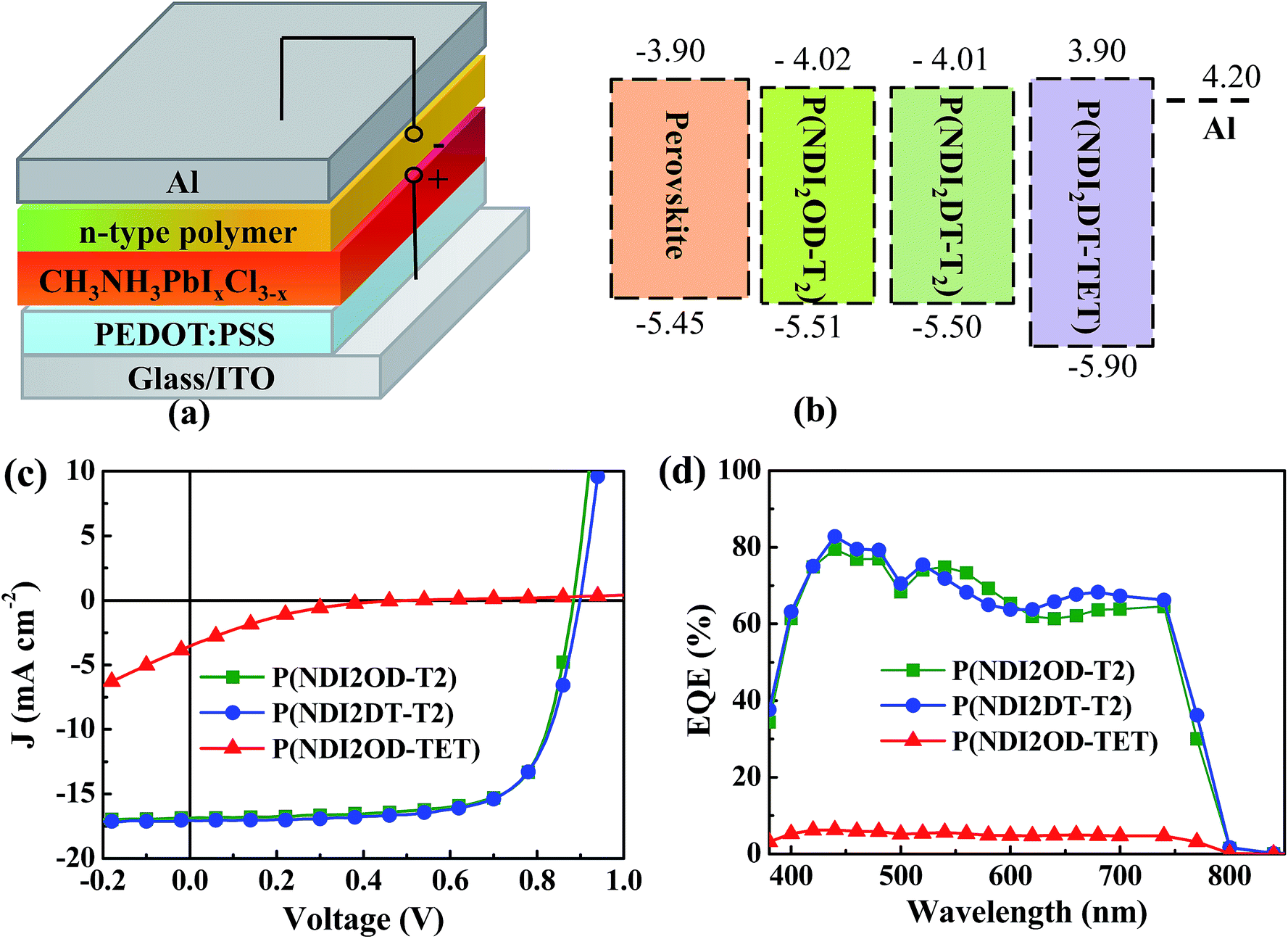 | ||
| Fig. 1 (a) Device structure of HPSCs described in this study. (b) Energy levels of the perovskite and of the three n-type polymers. (c) J–V curves under illumination and (d) EQE of the devices using the three different n-type polymers as EELs. | ||
The chemical structures of the three EEL n-type polymers, namely P(NDI2OD-T2), P(NDI2DT-T2) and P(NDI2OD-TET), are shown in Fig. S2a;† their synthesis is described in the ESI.†
Fig. S2b† shows the absorption spectra of the three polymers. P(NDI2OD-T2) and P(NDI2DT-T2) show similar absorption spectra with an onset of ∼850 nm, while P(NDI2OD-TET) shows an absorption onset at ∼650 nm. The corresponding optical band-gaps are 1.49, 1.49 and 2.1 eV, respectively. The electronic structures of the polymers were investigated by cyclic voltammetry (CV), as displayed in Fig. S2c.† From these measurements the LUMO levels of these polymers were estimated to be 4.01, 4.02 and 3.9 eV, respectively. Thus, the band-gap widening in P(NDI2OD-TET) is due to its lower highest occupied molecular orbital (HOMO) level (5.5 eV vs. 5.9 eV (see Fig. 1b)).
While the longer side chains of P(NDI2OD-T2) increase the solubility of the polymer without influencing the energy level and its band-gap. The ethyl unit in the backbone of P(NDI2OD-TET) reduces the conjugation length, which leads to a wider bandgap. In Fig. 1b it can be observed that all the three n-type polymers possess deeper-lying HOMO levels than the valence band of the perovskite film, while their LUMO levels are aligned with the conduction band of the hybrid perovskite. It is thus quite plausible that the n-type polymers will act as efficient hole blocking layers, while the alignment of the quasi-Fermi levels of the perovskite film and of the polymer will determine the sufficiency of the driving force for electron extraction.
Fig. 1c shows the current density (J)–voltage (V) characteristics under illumination of the HPSCs fabricated with our three polymers as EELs. In comparison to the device without EELs, which showed sub-linear J–V characteristics both in the dark and under illumination (Fig. S3†), the devices with EELs evidenced good rectification behaviour, indicating the importance of the interfacial layer. In order to investigate the origin of this difference, we compared the morphology of the perovskite films with and without the polymer EEL by atomic force microscopy (AFM) and scanning electron microscopy (SEM) measurements (Fig. S4†). The surface of the bare perovskite film was rather rough, with a root mean square (rms) of ∼16 nm, while the EEL coated HP films were far smoother, featuring a surface rms roughness of ∼4–6 nm. SEM images show that all the three n-type polymers could form continuous and dense films on top of the perovskite film. This finding confirms that the good processability of the EEL polymers enables smoother and continuous films to fully cover the underneath perovskite layer and helps filling in any pinholes present.
The device parameters obtained from the J–V characteristics are summarized in Table 1. The devices using P(NDI2OD-T2) and P(NDI2DT-T2) as EELs exhibited similar performances, with an open circuit voltage (VOC) of ∼0.8 V, a short circuit current density (JSC) of ∼17.0 mA cm−2, a fill factor (FF) of ∼0.7 and a PCE of ∼10.8%. Remarkably different is the device which uses P(NDI2OD-TET), showing much poorer performance, with a VOC of 0.71 V, a JSC of 1.41 mA cm−2, a FF of 0.18 and a PCE of 0.18%.
| Device | V OC [V] | J SC [mA cm−2] | FF | PCE [%] | R S [Ω cm−2] | R P [kΩ cm−2] |
|---|---|---|---|---|---|---|
| Without EEL | 0.08 | 0.000 | 0 | 0 | — | — |
| P(NDI2OD-T2) | 0.884 | 16.90 | 0.73 | 10.82 | 7.80 | 16.5 |
| P(NDI2DT-T2) | 0.899 | 17.10 | 0.71 | 10.83 | 9.20 | 10.0 |
| P(NDI2OD-TET) | 0.715 | 1.41 | 0.175 | 0.18 | 3411 | 25.0 |
The series resistance (RS) and shunt resistance (RP) of these devices were calculated from the dark J–V curves by fitting them with the Schottky equation as shown in Fig. S5.† It can be seen that the devices using P(NDI2OD-T2) and P(NDI2DT-T2) as EELs show RS values of 7.8 and 9.2 Ω cm−2, respectively. The device using P(NDI2OD-TET) as the EEL shows a very large RS of 3411 Ω cm−2, as indicated by the extremely low injection current measured in forward bias above the built-in voltage. The extremely high RS represents a large barrier for charge collection as well as severe recombination losses, leading to prominent features such as the low JSC and FF.
Electron injection from the EEL polymers into the Al electrode is assumed to be efficient due to favourable energy alignment. Given the fact that the same anode was used for these devices, RS variation for these cells should be caused only by the different energy barrier for electron extraction from the perovskite layer to the polymer or by limitations in the charge transport of the polymer film. The large RP values for the devices using the three n-type polymers as EELs demonstrate that all of these polymer films can effectively block the leakage current, as can be seen from the dark J–V characteristics showing very low current density under reverse and small forward bias. The effectiveness of the n-type polymers in blocking the leakage current is due to both the favourable energy alignment and the high quality films formed on top of the perovskite layer, as discussed previously.
Fig. 1d shows the external quantum efficiency (EQE) spectra of the devices fabricated with the three polymer EELs. It can be seen that the devices using P(NDI2OD-T2) and P(NDI2DT-T2) as EELs show much higher EQE values over the whole absorption range than the device using P(NDI2OD-TET) as the EEL, a finding also indicated by the J–V data.
Steady state and time resolved PL measurements were performed to investigate the influence of the n-type polymer EELs on charge extraction. As shown in Fig. 2a, the photoluminescence of the perovskite film is quenched significantly when the three polymers are deposited on top of it. In agreement with this observation, the PL lifetime of the perovskite film is also considerably reduced by the deposition of the three polymers (Fig. 2b). The pristine perovskite layer displays a mono-exponential decay, which can be fitted with a time constant of 21.2 ns. The heterostructured samples show substantially shorter lifetimes, with the perovskite/P(NDI2OD-TET) having a time constant of 8.7 ns, the perovskite/P(NDI2DT-T2) of 5.8 ns and the perovskite/P(NDI2OD-T2) of 4.8 ns. These results indicate that electrons are extracted from the perovskite film by all three polymers, even when the offset between the conduction band of the perovskite and the LUMO levels (0.11, 0.12 and 0 eV) are very limited. In addition, we noted that the interface with P(NDI2OD-TET) is less efficient in reducing the recombination of electrons and holes in the perovskite, even when a reduction of the lifetime superior to a factor 2 is recorded. The energy level alignment between the perovskite and the polymer is very similar for all the three devices, though this is not necessarily the limiting factor that explains the discrepancy of the device performance.
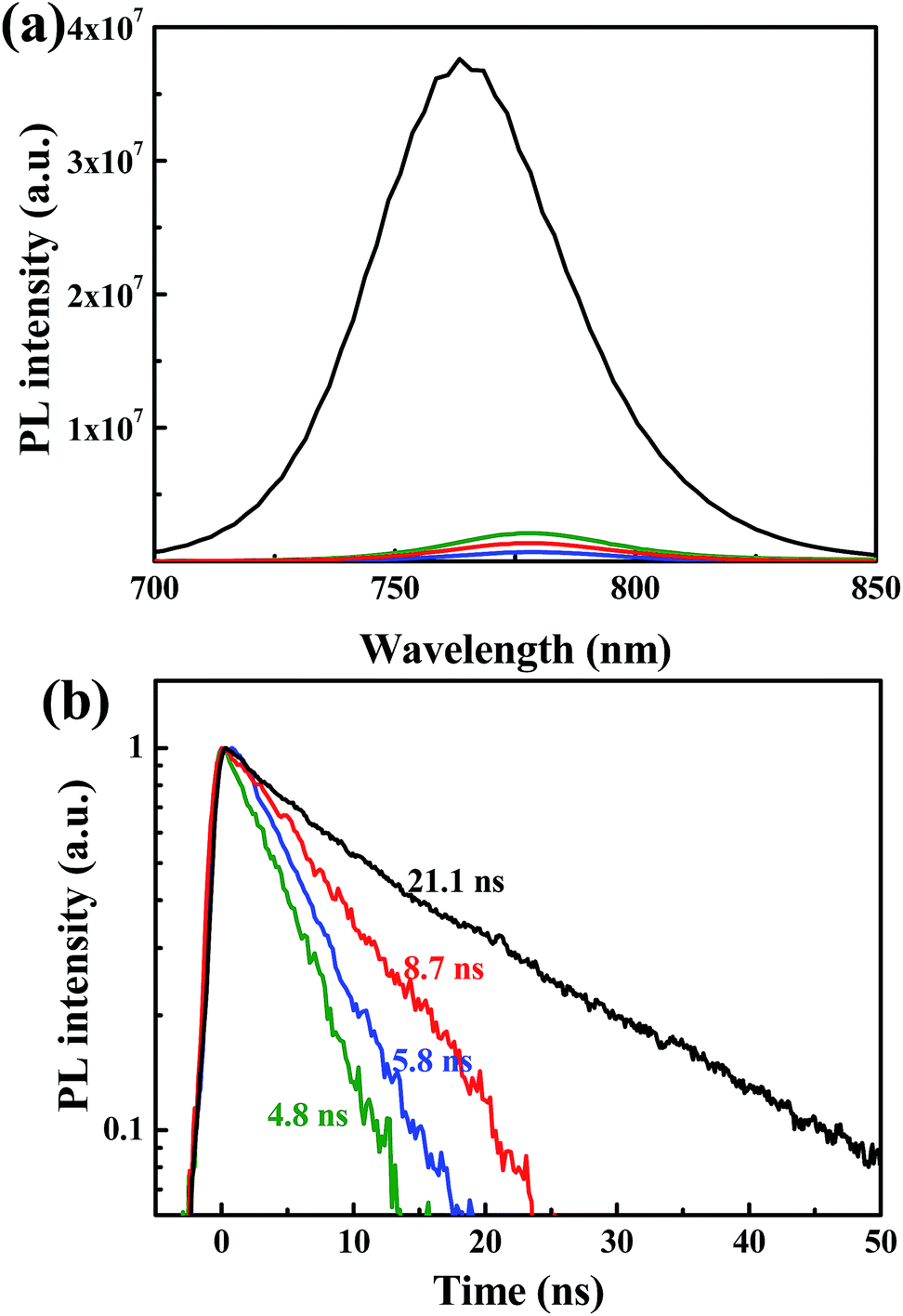 | ||
| Fig. 2 (a) Steady state spectra and (b) time resolved PL decays for perovskite films without (black line) and with the n-type polymer on top (green line for P(NDI2OD-T2), blue line for P(NDI2DT-T2), and red line for P(NDI2OD-TET)). | ||
Obviously the large series resistance measured in the case of the sample featuring P(NDI2OD-TET) indicates that a possible source of dissimilarity in behaviour between the three polymers might be their electron-transport capacity. For this purpose we investigated the electron transport in P(NDI2OD-T2), P(NDI2DT-T2) and P(NDI2OD-TET) films by measuring the dark J–V characteristics in electron-only devices. These devices were fabricated as described in the Experimental Section, by sandwiching the polymer layer between Al and LiF/Al chosen to suppress the injection of holes into the HOMO of the polymer. The space-charge limited current in these devices is a function of the voltage, the film thickness and the electron mobility.51 We fitted the experimental J–V curves with the equation.51
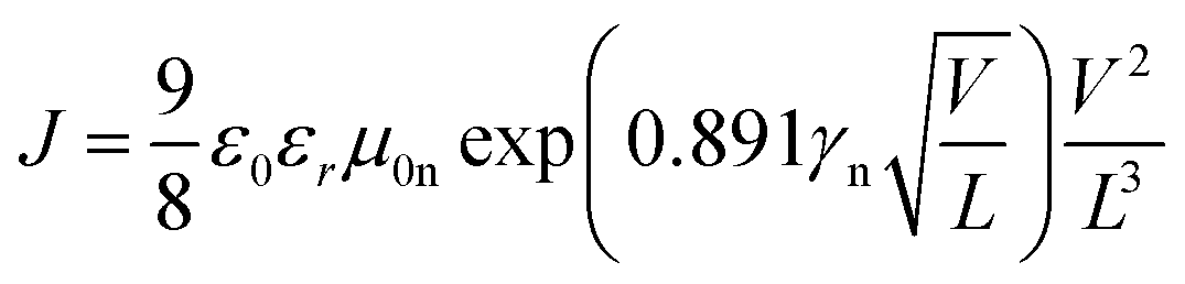 | (1) |
To gain further insight into the charge recombination mechanism in HPSCs with different n-type polymer EELs, we investigated the light intensity-dependent J–V characteristics. The dependence of JSC on the light intensity is shown in Fig. 3a. From the Schottky equation it is easy to derive that:
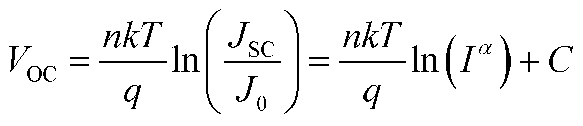 | (2) |
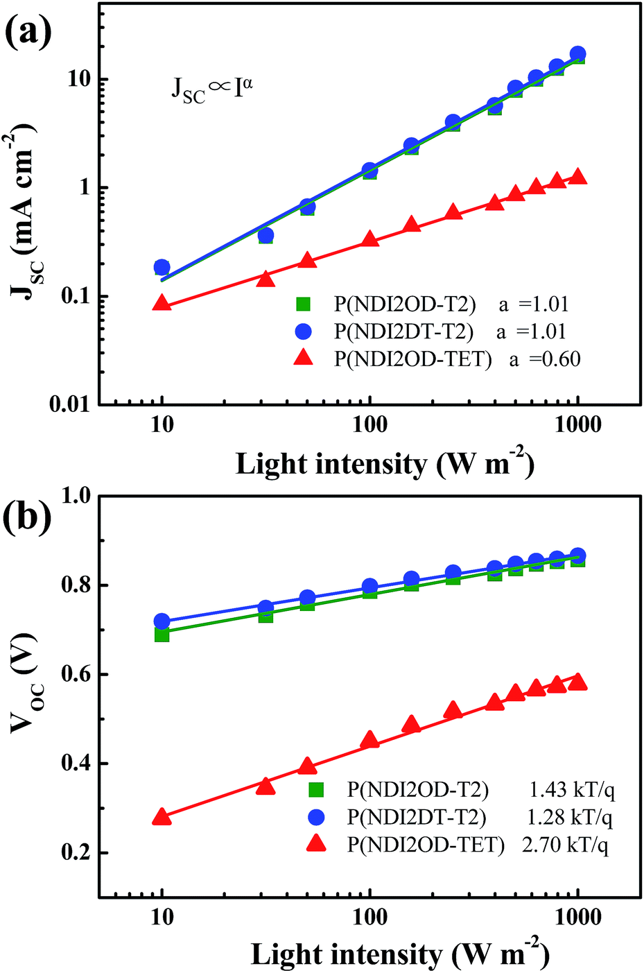 | ||
| Fig. 3 Light intensity dependence of (a) the photocurrent density and of (b) the open circuit voltage of the HPSCs using different n-type polymers as EELs. Solid symbols represent experimental data and solid lines are fitting results. | ||
Fig. 3b shows the dependence of VOC on the light intensity in the three different device structures (as from eqn (2)). At room temperature the slopes of the plot showing the VOCvs. the logarithm of the light-intensity in the devices with P(NDI2OD-T2), P(NDI2DT-T2) and P(NDI2OD-TET) are calculated to be 1.43 kT/q, 1.28 kT/q and 2.70 kT/q, respectively. In the absence of trap-assisted recombination, the slope should be kT/q. The deviation from the ideal value indicates that trap-assisted charge recombination takes place in all of these devices. Such a recombination process has also been reported in fullerene-based HPSCs being determined by the trap states in the HP layer and regarded as the dominant recombination pathway.53
While, the devices using P(NDI2OD-T2) and P(NDI2DT-T2) as EELs show a similar level of trap assisted recombination, the device using the P(NDI2OD-TET) EEL shows much higher trap assisted recombination. As mentioned above, the transferred electrons cannot be extracted from the P(NDI2OD-TET) EEL due to its poor transport capability and have the tendency to accumulate at the perovskite/EEL interface, leading to a higher possibility for these electrons to be trapped at the perovskite interface. Therefore, the synergetic effects of trap-assisted recombination and bimolecular recombination lead to severe loss in PCE of the device using P(NDI2OD-TET) as the EEL.
Besides the efficiency, it is highly relevant to investigate the stability under ambient conditions of HPSCs with different EELs. Fig. 4 shows the variation with time of the VOC, JSC, FF and PCE for HPSCs using P(NDI2OD-T2) and PC60BM as EELs stored under ambient conditions. The fresh device using PC60BM as the EEL showed a VOC of 0.87 V, a JSC of 17.64 mA cm−2, a FF of 0.75 and a PCE of 11.29% (Fig. S7†). After 270 minutes of exposure to air, the VOC decayed to 92% of its original value, while JSC and FF decayed to 24% and 17% of original values, respectively. As a result, the PCE reduced to 3.5% of the original value. The device using P(NDI2OD-T2) as the EEL showed instead much more stable performance compared to that using PC60BM as the EEL. After the same period of exposure to ambient conditions, VOC and JSC retained 94% and 90% of the initial values, while the FF increased slightly respect to the initial value. Consequently, the PCE became 87% of its initial value.
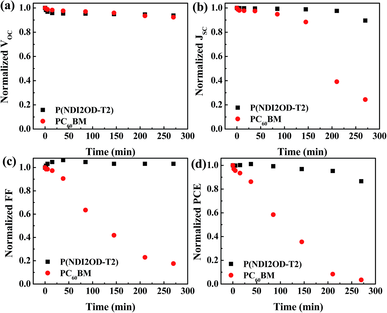 | ||
| Fig. 4 Variation with time of (a) VOC, (b) JSC, (c) FF and (d) PCE of the HPSCs using P(NDI2OD-T2) and PC60BM as EELs. | ||
Fig. S8† shows the AFM and SEM images of the PC60BM-coated HP layer. PC60BM also forms a continuous and dense film on top of the perovskite layer, which has a surface rms roughness of 4.1 nm. Therefore, the surface morphology of the EEL cannot explain the huge difference in the device stability. Fig. 5 shows optical micrographs of the devices using P(NDI2OD-T2) and PC60BM as EELs before and after exposure to ambient conditions. The fresh devices show continuous Al electrodes without corrosion. After storage under ambient conditions, the Al electrode of the device using PC60BM appeared severely damaged, while the Al electrode of the device using P(NDI2OD-T2) as the EEL appears only slightly damaged. Fig. S9† shows the optical micrographs of the P(NDI2OD-T2) and PC60BM covered perovskite films before and after exposure to air. The P(NDI2OD-T2) covered perovskite film shows no obvious change in the morphology, while PC60BM covered perovskite film shows a myriad of particles of diameter larger than 1 μm, which could be the methylammonium iodide resulting from the decomposition of the perovskite film induced by water. A possible explanation for the degradation is that PC60BM enables water to diffuse into the perovskite layer leading to the decomposition of the underneath perovskite film.43,44 Moreover, methylammonium iodide produced during the decomposition of the perovskite film can react with the Al electrode (as evidenced in Fig. 5d), leading to a large series resistance for charge collection and severe loss in device performance. In contrast, the n-type polymer film can prevent the diffusion of water into the perovskite film, acting as an effective encapsulation layer leading to improved device stability under ambient conditions.54
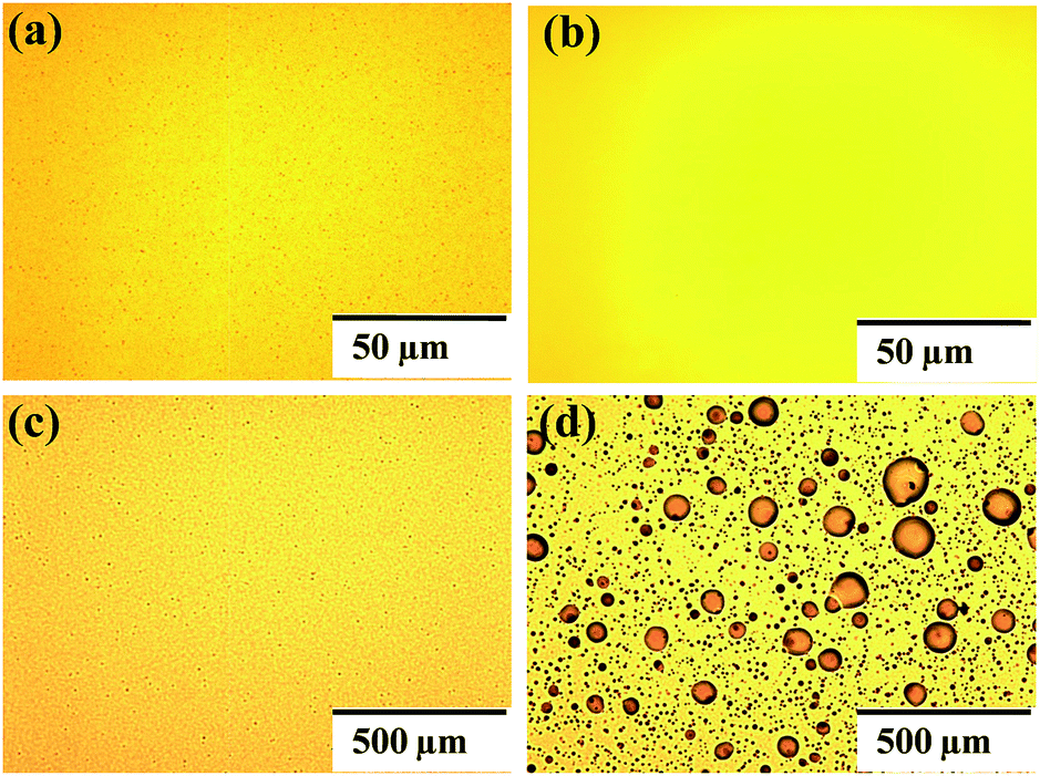 | ||
| Fig. 5 Optical micrographs of the Al electrode of HPSCs using P(NDI2OD-T2) and PC60BM as EELs (a), (b) before (c), and (d) after exposure to ambient conditions. | ||
Conclusions
We investigated how the structural, photophysical and charge transport properties of the perovskite/n-type polymer EEL interface affect the HPSC device performance. The devices using P(NDI2OD-T2) and P(NDI2DT-T2) as EELs showed PCEs ∼10.8%, whereas the device using P(NDI2OD-TET) as the EEL showed a low PCE of only 0.18%. Even though the offsets between the conduction band of the perovskite and the polymer LUMOs were quite small, optical measurements confirmed the efficient extraction of electrons. Our results also indicate that the EELs affect the charge recombination mechanism in HPSCs. Trap assisted recombination was evidenced in devices using all the three n-type polymers as EELs. Bimolecular recombination in the devices using the high mobility n-type polymers P(NDI2OD-T2) and P(NDI2DT-T2) was negligible, while the bimolecular recombination was very severe in the devices using the low mobility n-type polymer P(NDI2OD-TET), thus rationalizing the corresponding device performance. We conclude that the EEL bulk electron mobility, rather than the energy offset between the perovskite and the EEL LUMO energy, plays a dominant role in the charge collection in HPSCs. In addition, we showed that the ambient stability of the HPSCs was considerably improved by using n-type polymers as EELs, which acted as effective encapsulation layers towards water penetration.Acknowledgements
This work is financed by the European Commission, Marie Curie Actions-Intra-European Fellowships (IEF) “SECQDSC” No. 626852 and European Research Council, ERC Starting Grant “HySPOD” No. 306983. The work of D. B. forms a part of the research programme of the Dutch Polymer Institute (DPI), project number 734. The technical support of A. Kamp is highly appreciated. We would like to thank T. T. M. Palstra for inspiring discussions.Notes and references
- J.-W. Lee, D.-J. Seol, A.-N. Cho and N.-G. Park, Adv. Mater., 2014, 26, 4991 CrossRef CAS PubMed.
- F. Hao, C. C. Stoumpos, R. P. H. Chang and M. G. Kanatzidis, J. Am. Chem. Soc., 2014, 136, 8094 CrossRef CAS PubMed.
- P.-W. Liang, C.-C. Chueh, X.-K. Xin, F. Zuo, S. T. Williams, C.-Y. Liao and A. K. Y. Jen, Adv. Energy Mater., 2015, 5, 1400960 Search PubMed.
- J. M. Ball, S. D. Stranks, M. T. Horantner, S. Huttner, W. Zhang, E. J. W. Crossland, I. Ramirez, M. Riede, M. B. Johnston, R. H. Friend and H. J. Snaith, Energy Environ. Sci., 2015, 8, 602 CAS.
- Q. Lin, A. Armin, R. C. R. Nagiri, P. L. Burn and P. Meredith, Nat. Photonics, 2015, 9, 106 CrossRef CAS.
- J. H. Heo, D. H. Song and S. H. Im, Adv. Mater., 2014, 26, 8179 CrossRef CAS PubMed.
- N. Pellet, P. Gao, G. Gregori, T.-Y. Yang, M. K. Nazeeruddin, J. Maier and M. Grätzel, Angew. Chem., Int. Ed., 2014, 53, 3151 CrossRef CAS PubMed.
- Y. Chen, J. Peng, D. Su, X. Chen and Z. Liang, ACS Appl. Mater. Interfaces, 2015, 7, 4471 CAS.
- S. D. Stranks, G. E. Eperon, G. Grancini, C. Menelaou, M. J. P. Alcocer, T. Leijtens, L. M. Herz, A. Petrozza and H. J. Snaith, Science, 2013, 342, 341 CrossRef CAS PubMed.
- G. Xing, N. Mathews, S. Sun, S. S. Lim, Y. M. Lam, M. Grätzel, S. Mhaisalkar and T. C. Sum, Science, 2013, 342, 344 CrossRef CAS PubMed.
- A. Kojima, K. Teshima, Y. Shirai and T. Miyasaka, J. Am. Chem. Soc., 2009, 131, 6050 CrossRef CAS PubMed.
- H.-S. Kim, C.-R. Lee, J.-H. Im, K.-B. Lee, T. Moehl, A. Marchioro, S.-J. Moon, R. Humphry-Baker, J.-H. Yum, J. E. Moser, M. Gratzel and N.-G. Park, Sci. Rep., 2012, 2, 591 Search PubMed.
- M. M. Lee, J. Teuscher, T. Miyasaka, T. N. Murakami and H. J. Snaith, Science, 2012, 338, 643 CrossRef CAS PubMed.
- M. Liu, M. B. Johnston and H. J. Snaith, Nature, 2013, 501, 395 CrossRef CAS PubMed.
- K.-C. Wang, J.-Y. Jeng, P.-S. Shen, Y.-C. Chang, E. W.-G. Diau, C.-H. Tsai, T.-Y. Chao, H.-C. Hsu, P.-Y. Lin, P. Chen, T.-F. Guo and T.-C. Wen, Sci. Rep., 2014, 4, 4756 Search PubMed.
- J. Burschka, N. Pellet, S.-J. Moon, R. Humphry-Baker, P. Gao, M. K. Nazeeruddin and M. Gratzel, Nature, 2013, 499, 316 CrossRef CAS PubMed.
- H. Yu, X. Liu, Y. Xia, Q. Dong, K. Zhang, Z. Wang, Y. Zhou, B. Song and Y. Li, J. Mater. Chem. A, 2016, 4, 321 CAS.
- H. Zhang, J. Mao, H. He, D. Zhang, H. L. Zhu, F. Xie, K. S. Wong, M. Grätzel and W. C. H. Choy, Adv. Energy Mater., 2015, 1501354 Search PubMed.
- Z. Xiao, Q. Dong, C. Bi, Y. Shao, Y. Yuan and J. Huang, Adv. Mater., 2014, 26, 6503 CrossRef CAS PubMed.
- N. J. Jeon, J. H. Noh, Y. C. Kim, W. S. Yang, S. Ryu and S. I. Seok, Nat. Mater., 2014, 13, 897 CrossRef CAS PubMed.
- Y. Wu, A. Islam, X. Yang, C. Qin, J. Liu, K. Zhang, W. Peng and L. Han, Energy Environ. Sci., 2014, 7, 2934 CAS.
- W. Nie, H. Tsai, R. Asadpour, J.-C. Blancon, A. J. Neukirch, G. Gupta, J. J. Crochet, M. Chhowalla, S. Tretiak, M. A. Alam, H.-L. Wang and A. D. Mohite, Science, 2015, 347, 522 CrossRef CAS PubMed.
- Q. Chen, H. Zhou, Z. Hong, S. Luo, H.-S. Duan, H.-H. Wang, Y. Liu, G. Li and Y. Yang, J. Am. Chem. Soc., 2014, 136, 622 CrossRef CAS PubMed.
- Q. Liang, J. Liu, Z. Cheng, Y. Li, L. Chen, R. Zhang, J. Zhang and Y. Han, J. Mater. Chem. A, 2016, 4, 223 CAS.
- W. S. Yang, J. H. Noh, N. J. Jeon, Y. C. Kim, S. Ryu, J. Seo and S. I. Seok, Science, 2015, 348, 1234 CrossRef CAS PubMed.
- Z. Xiao, C. Bi, Y. Shao, Q. Dong, Q. Wang, Y. Yuan, C. Wang, Y. Gao and J. Huang, Energy Environ. Sci., 2014, 7, 2619 CAS.
- A. Mei, X. Li, L. Liu, Z. Ku, T. Liu, Y. Rong, M. Xu, M. Hu, J. Chen, Y. Yang, M. Grätzel and H. Han, Science, 2014, 345, 295–298 CrossRef CAS PubMed.
- Y. Liu, Q. Chen, H.-S. Duan, H. Zhou, Y. Yang, H. Chen, S. Luo, T.-B. Song, L. Dou and Z. Hong, J. Mater. Chem. A, 2015, 3, 11940 CAS.
- O. Malinkiewicz, A. Yella, Y. H. Lee, G. M. Espallargas, M. Graetzel, M. K. Nazeeruddin and H. J. Bolink, Nat. Photonics, 2014, 8, 128 CrossRef CAS.
- H. Choi, C.-K. Mai, H.-B. Kim, J. Jeong, S. Song, G. C. Bazan, J. Y. Kim and A. J. Heeger, Nat. Commun., 2015, 6 Search PubMed.
- Y. Bai, H. Yu, Z. Zhu, K. Jiang, T. Zhang, N. Zhao, S. Yang and H. Yan, J. Mater. Chem. A, 2015, 3, 9098 CAS.
- J. Min, Z.-G. Zhang, Y. Hou, C. O. Ramirez Quiroz, T. Przybilla, C. Bronnbauer, F. Guo, K. Forberich, H. Azimi, T. Ameri, E. Spiecker, Y. Li and C. J. Brabec, Chem. Mater., 2015, 27, 227 CrossRef CAS.
- H. Zhou, Q. Chen, G. Li, S. Luo, T.-b. Song, H.-S. Duan, Z. Hong, J. You, Y. Liu and Y. Yang, Science, 2014, 345, 542 CrossRef CAS PubMed.
- J. H. Heo, H. J. Han, D. Kim, T. K. Ahn and S. H. Im, Energy Environ. Sci., 2015, 8, 1602 CAS.
- Y. Shao, Z. Xiao, C. Bi, Y. Yuan and J. Huang, Nat. Commun., 2014, 5 Search PubMed.
- H. Dong, Z. Wu, B. Xia, J. Xi, F. Yuan, S. Ning, L. Xiao and X. Hou, Chem. Commun., 2015, 51, 8986 RSC.
- J.-Y. Jeng, Y.-F. Chiang, M.-H. Lee, S.-R. Peng, T.-F. Guo, P. Chen and T.-C. Wen, Adv. Mater., 2013, 25, 3727 CrossRef CAS PubMed.
- M. Hu, C. Bi, Y. Yuan, Z. Xiao, Q. Dong, Y. Shao and J. Huang, Small, 2015, 11, 2164 CrossRef CAS PubMed.
- H. Azimi, T. Ameri, H. Zhang, Y. Hou, C. O. R. Quiroz, J. Min, M. Hu, Z.-G. Zhang, T. Przybilla, G. J. Matt, E. Spiecker, Y. Li and C. J. Brabec, Adv. Energy Mater., 2015, 5, 1570042 Search PubMed.
- Q. Xue, Z. Hu, J. Liu, J. Lin, C. Sun, Z. Chen, C. Duan, J. Wang, C. Liao, W. M. Lau, F. Huang, H.-L. Yip and Y. Cao, J. Mater. Chem. A, 2014, 2, 19598 CAS.
- H.-H. Wang, Q. Chen, H. Zhou, L. Song, Z. S. Louis, N. D. Marco, Y. Fang, P. Sun, T.-B. Song, H. Chen and Y. Yang, J. Mater. Chem. A, 2015, 3, 9108 CAS.
- C. Liu, K. Wang, P. Du, T. Meng, X. Yu, S. Z. D. Cheng and X. Gong, ACS Appl. Mater. Interfaces, 2015, 7, 1153 CAS.
- J. You, L. Meng, T.-B. Song, T.-F. Guo, Y. Yang, W.-H. Chang, Z. Hong, H. Chen, H. Zhou, Q. Chen, Y. Liu, N. D. Marco and Y. Yang, Nat. Nanotechnol., 2016, 11, 75 CrossRef CAS PubMed.
- Q. Bao, X. Liu, S. Braun and M. Fahlman, Adv. Energy Mater., 2014, 4, 1301272 Search PubMed.
- C. Mu, P. Liu, W. Ma, K. Jiang, J. Zhao, K. Zhang, Z. Chen, Z. Wei, Y. Yi, J. Wang, S. Yang, F. Huang, A. Facchetti, H. Ade and H. Yan, Adv. Mater., 2014, 26, 7224–7230 CrossRef CAS PubMed.
- S. Dai, P. Cheng, Y. Lin, Y. Wang, L. Ma, Q. Ling and X. Zhan, Polym. Chem., 2015, 6, 5254–5263 RSC.
- Y. Zhou, T. Kurosawa, W. Ma, Y. Guo, L. Fang, K. Vandewal, Y. Diao, C. Wang, Q. Yan, J. Reinspach, J. Mei, A. L. Appleton, G. I. Koleilat, Y. Gao, S. C. B. Mannsfeld, A. Salleo, H. Ade, D. Zhao and Z. Bao, Adv. Mater., 2014, 26, 3767–3772 CrossRef CAS PubMed.
- W. Wang, J. Yuan, G. Shi, X. Zhu, S. Shi, Z. Liu, L. Han, H.-Q. Wang and W. Ma, ACS Appl. Mater. Interfaces, 2015, 7, 3994 CAS.
- Z. Tang, B. Liu, A. Melianas, J. Bergqvist, W. Tress, Q. Bao, D. Qian, O. Inganäs and F. Zhang, Adv. Mater., 2015, 27, 1900–1907 CrossRef CAS PubMed.
- W. Wang, J. Yuan, G. Shi, X. Zhu, S. Shi, Z. Liu, L. Han, H.-Q. Wang and W. Ma, ACS Appl. Mater. Interfaces, 2015, 7, 3994–3999 CAS.
- J. Liu, S. Shao, G. Fang, B. Meng, Z. Xie and L. Wang, Adv. Mater., 2012, 24, 2774 CrossRef CAS PubMed.
- C. S. Ponseca, T. J. Savenije, M. Abdellah, K. Zheng, A. Yartsev, T. Pascher, T. Harlang, P. Chabera, T. Pullerits, A. Stepanov, J.-P. Wolf and V. Sundström, J. Am. Chem. Soc., 2014, 136, 5189 CrossRef CAS PubMed.
- G.-J. A. H. Wetzelaer, M. Scheepers, A. M. Sempere, C. Momblona, J. Ávila and H. J. Bolink, Adv. Mater., 2015, 27, 1837 CrossRef CAS PubMed.
- Z. Xu, L.-M. Chen, G. Yang, C.-H. Huang, J. Hou, Y. Wu, G. Li, C.-S. Hsu and Y. Yang, Adv. Funct. Mater., 2009, 19, 1227–1234 CrossRef CAS.
Footnote |
| † Electronic supplementary information (ESI) available. See DOI: 10.1039/c5ta10696f |
| This journal is © The Royal Society of Chemistry 2016 |