
 Open Access Article
 This Open Access Article is licensed under a
 Creative Commons Attribution 3.0 Unported Licence
Evolution of ferroelectric domains in methylammonium lead iodide and correlation with the performance of perovskite solar cells†
Tobias
Leonhard
ab,
Holger
Röhm
 ab,
Fabian J.
Altermann
c,
Michael J.
Hoffmann
ac and
Alexander
Colsmann
*ab
ab,
Fabian J.
Altermann
c,
Michael J.
Hoffmann
ac and
Alexander
Colsmann
*ab
aKarlsruhe Institute of Technology, Material Research Center for Energy Systems (MZE), Strasse am Forum 7, 76131 Karlsruhe, Germany. E-mail: alexander.colsmann@kit.edu
bKarlsruhe Institute of Technology, Light Technology Institute (LTI), Engesserstrasse 13, 76131 Karlsruhe, Germany
cKarlsruhe Institute of Technology, Institute for Applied Materials – Ceramic Materials and Technologies (IAM), Haid-und-Neu-Strasse 7, 76131 Karlsruhe, Germany
First published on 31st August 2021
Abstract
While more and more experimental evidence for the ferroelectricity of methylammonium lead iodide (MAPbI3) is being reported in the literature, the scientific community still controversially discusses whether or not the ferroelectric polarization has any influence on the performance of perovskite solar cells. In this work, the evolution of ferroelectric domains and their polarization orientation in MAPbI3 thin films during thermal annealing are investigated using piezoresponse force microscopy (PFM) and Kelvin probe force microscopy (KPFM). Right after deposition and annealing for 5 s, small grains with non-uniform crystal orientation and polarization are formed. During the next 30–60 s, these small grains increase in diameter and large ferroelectric domains with out-of-plane polarization appear. In the annealing regime of several minutes to one hour, these large grains produce uniform domains with alternating in-plane polarization and (110) texture. The corresponding MAPbI3 solar cells show a distinct performance enhancement and improved operational stability if the ferroelectric polarization is oriented in-plane. In contrast, solar cells with out-of-plane-polarized MAPbI3 exhibit only moderate fill factors and reduced open-circuit voltages.
1 Introduction
Organic metal halide perovskites (OMH) are one of the most exciting material classes of the last decade which find their application in perovskite solar cells, light-emitting diodes and other optoelectronic applications. The remarkable photovoltaic performance of polycrystalline OMH thin-films has its origin in efficient charge carrier transport and low recombination losses.1–3 In order to unravel the fundamental mechanisms behind these exceptional charge carrier dynamics, several computational studies investigated the crystal properties of the archetypical methylammonium lead iodide (CH3NH3PbI3, MAPbI3) and suggested that MAPbI3 may be ferroelectric.4–6 By definition, ferroelectric materials exhibit a spontaneous polarization, which can be reversed or aligned under an external electric field.7,8 This spontaneous and adjustable polarization triggers the formation of polar domains with alternating polarization.9 According to simulations, the microscopic electrical fields within these domains can help the efficient charge carrier separation.10–12 At the same time, channel-like pathways are created in the crystal, which transport the photo-generated charge carriers towards the respective electrodes along safe pathways.On the experimental side, in early works, MAPbI3 thin-films were investigated for ferroelectricity mostly by resonance-enhanced piezoresponse force microscopy (PFM), consistently showing striped domain patterns with alternating piezoresponse.13,14 The interpretation of this alternating piezoresponse, however, fueled a vivid debate on the ferroic properties of MAPbI3. While the alternating piezoresponse of domain assemblies generally is indicative of ferroelectricity, it was rightfully pointed out that the resonance enhancement during PFM measurements may induce measurement artefacts.15–17 Also, mobile ionic charges may populate the surface of the MAPbI3 layer and corrupt the measurement data.18 While these are valid concerns, more recently, other observations and material properties were reported and correlated with PFM data in favor of ferroelectricity. These data include anisotropy of the PFM signal in vertical and horizontal direction,19 a correlation of the piezoresponse with the c-axis of the tetragonal crystal,19 a surface potential modulation of occasional out-of-plane polarized domains20 and the displacement of iodine in the tetragonal unit cell, creating an electrical dipole.21 In addition, the switching of domains and shifting of domain walls under external polarizing electrical fields22 as well as a hysteresis loop at lower temperature were observed.23 Notably, MAPbI3 is a semiconductor which exhibits properties that are somewhat different from classical ferroelectric dielectrics, e.g., external polarization fields have to be rather weak to not destroy the crystal (creeping poling).22,24 The effects occurring in a ferroelectric semiconductor must not be confused with the bulk-photovoltaic effect which only occurs in dielectrics.25,26 Although controversial discussions surrounding the ferroelectric or non-ferroelectric nature of MAPbI3 continue to fill the scientific literature,27–33 the authors of this study consider the comprehensive set of experimental findings compelling in favor of ferroelectricity. So far, no other theory can explain all of the observed domain and material properties. This is why we henceforth discuss our experimental findings in light of MAPbI3 being a ferroelectric semiconductor.
The discussion surrounding the ferroelectricity of MAPbI3 is often considered purely academic as, to date, no experimental evidence was produced of the impact of the ferroelectric domains on the solar cell performance. In this work, we set out to experimentally correlate ferroelectric polarization and solar cell performance. To this end, we investigate the formation and evolution of ferroelectric domains during the fabrication of polycrystalline MAPbI3 thin-films and subsequently build solar cells from these samples. The analysis of the microstructure reveals that the duration of thermal annealing, which is a common step in nearly all manufacturing processes of OMH perovskite solar cells, is decisive for the domain formation and the orientation of the polarization. We attribute the observed changes of the domain structure to an interplay of mechanical stress and depolarizing fields during grain growth and thin-film formation.34 In particular, the sample cooling below the Curie temperature TC (MAPbI3: TC = 55 °C (ref. 35)) plays a critical role in this process, since the cubic-to-tetragonal phase transition leads to mechanical strain and spontaneous polarization PS. Solar cells incorporating MAPbI3 layers with different polarization orientations show distinctly different current density–voltage (J–V) characteristics.
2 Results and discussion
2.1 Ferroelectric domains
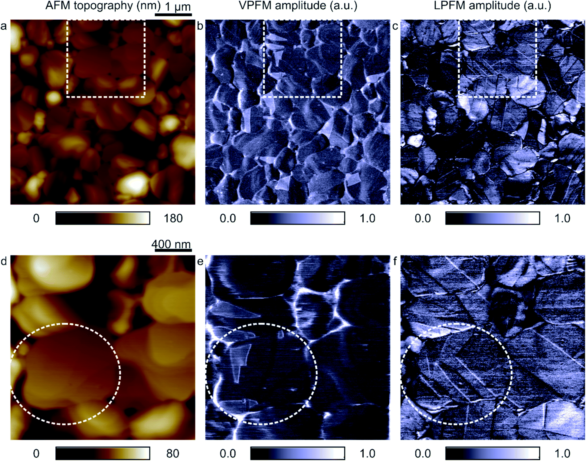
All our experiments were carried out on MAPbI3 layers with a thickness of 300 nm as commonly implemented as light harvesting layers in solar cells. MAPbI3 was deposited from lead iodide (PbI2) and methylammonium iodide (MAI) in a two-step process onto a glass/indium tin oxide (ITO)/poly(3,4-ethylenedioxythiophene):polystyrenesulfonate (PEDOT:PSS) substrate as described in our previous studies.14,19 Then the samples were thermally annealed at 100 °C under solvent vapor atmosphere that was maintained by covering each sample with a small Petri dish (volume approx. 5 cm3). The microstructure of grains and the domain formation were then assigned to the different annealing times. We used piezoresponse force microscopy (PFM) as a versatile characterization tool that allows probing of out-of-plane (vertical PFM; VPFM) and in-plane (lateral PFM; LPFM) piezoresponse independently. In combination with standard atomic force microscopy (AFM), PFM further lets us explore the relation between grain growth and ferroelectric domain formation. Notably, upon continuous measurements of the piezoresponse of the sample under an external electrical bias, the soft MAPbI3 layers may be damaged, allowing only a limited number of PFM measurements at each sample position. Since any long-term exposure to humid air during characterization can damage the perovskite samples, all fabrication and characterization steps were conducted in an inert nitrogen atmosphere inside a glovebox. Yet, the sample position had to be changed between different sets of measurements.Fig. 1, row 1 depicts a series of AFM topography images of five MAPbI3 samples that were fabricated using identical processing parameters, but different annealing times after the initial precursor-to-perovskite conversion that occurs within the first 5 s of annealing: sample 1 → 5 s; sample 2 → 30 s; sample 3 → 60 s; sample 4 → 3 min; sample 5 → 60 min. Throughout this series of five samples, we observed continuous grain growth towards longer annealing times, mediated by the solvent atmosphere under the Petri dish. This grain growth is most significant within the first 30 s of annealing. While 5 s of annealing formed small roundish grains with a diameter of 200–300 nm, 30 s and 60 s of annealing resulted in more flat grains with higher diameter that replaced some of the small grains with diameters below 300 nm (see ESI Fig. S1† for a statistical analysis). Annealing for several minutes led to coalescence of grains for diameters of several micrometers.
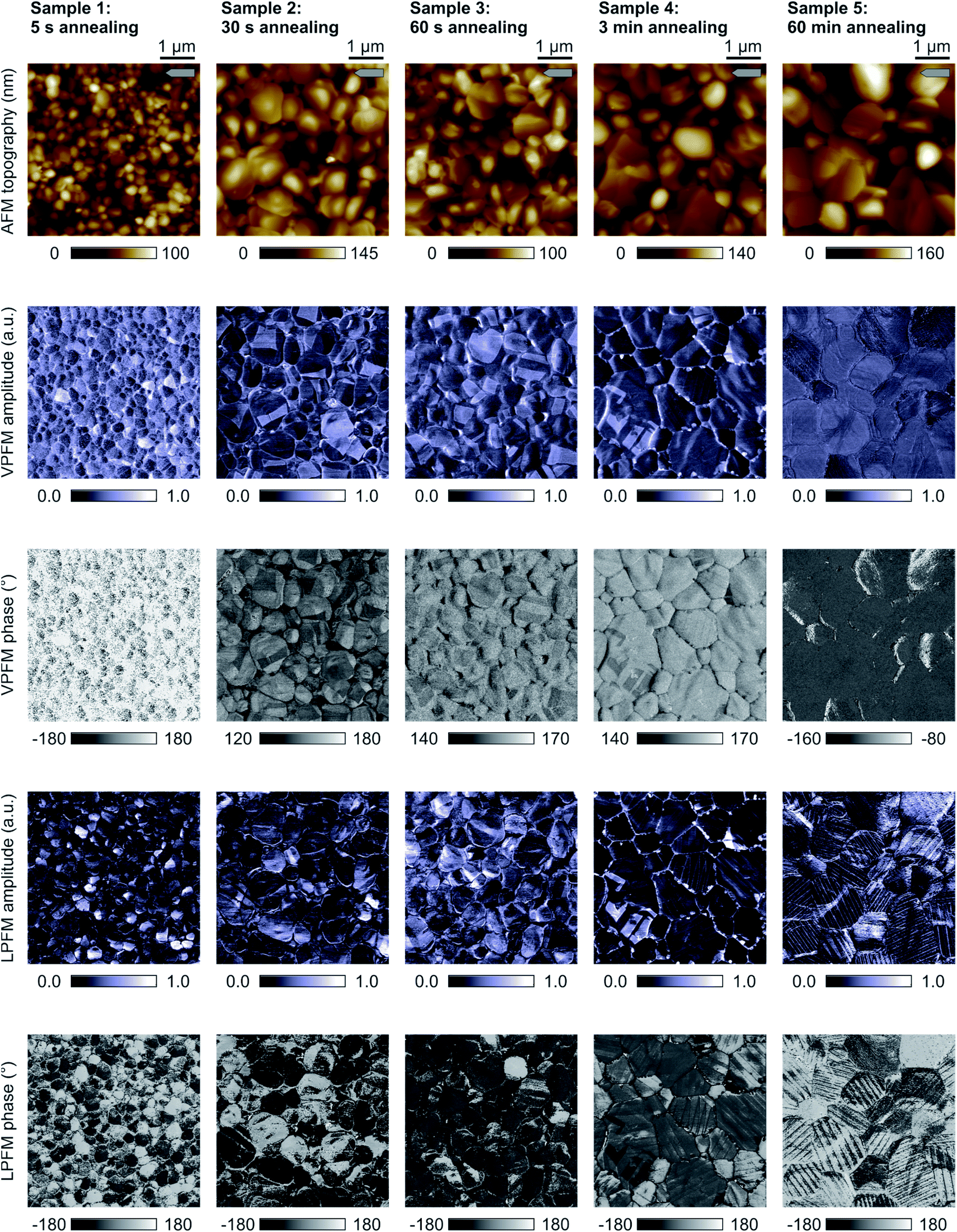 | ||
| Fig. 1 Effects of thermal annealing on the microstructure of polycrystalline MAPbI3 thin-films. Samples 1–5 (columns from left to right) were exposed to thermal annealing for 5 s, 30 s, 60 s, 3 min and 60 min, which caused modifications to grain sizes and domain structures. The rows represent the AFM topography, VPFM amplitude, VPFM phase, LPFM amplitude, LPFM phase. The cantilever orientation is indicated by the small grey arrow. Most of the grain growth occurs during the first 30 seconds of annealing (samples 1 and 2). Due to small grain diameters and various surface facets, each grain in sample 1 comprises uniform out-of-plane and in-plane ferroelectric polarization components. Upon longer annealing and grain growth, the polarization changes and evolves towards a predominant in-plane orientation with alternating domains (sample 5). | ||
The annealing time does not only determine the grain size but also the crystallographic properties of the MAPbI3 grains. The X-ray diffraction (XRD) measurements on samples that were annealed for 5 s, 30 s and 60 min (equivalent to samples 1, 2 and 5 in Fig. 1) in Fig. 2 provide an integrated information of the grain orientation of the layer. The data in Fig. 2a confirms that, after five seconds, the conversion of the precursor to perovskite is complete and no notable precursor residues persist. The diffractograms also show the evolution of the orientation. After 5 s, we find mostly non-uniformly oriented grains with some minor texture in [002] and [110] direction. After longer annealing for 30 s (Fig. 2b), together with an increase of grain size and crystallinity, we still observe the coexistence of (002) and (110) orientations with an enhancement of the (002) peak. After 60 min (Fig. 2c), the (110) peak and orientation prevail while the (002) peak and orientation have vanished, which is in accordance with the predominant (110) texture that was reported in previous work on MAPbI3 absorber layers that were optimized for solar cell integration.19 A (001) texture implies that the c-axis of the tetragonal perovskite unit cell is oriented out-of-plane, i.e., the c-axis is oriented perpendicular to the substrate, whereas a (110) texture corresponds to the c-axis being in-plane, i.e. the c-axis is oriented parallel to the substrate.
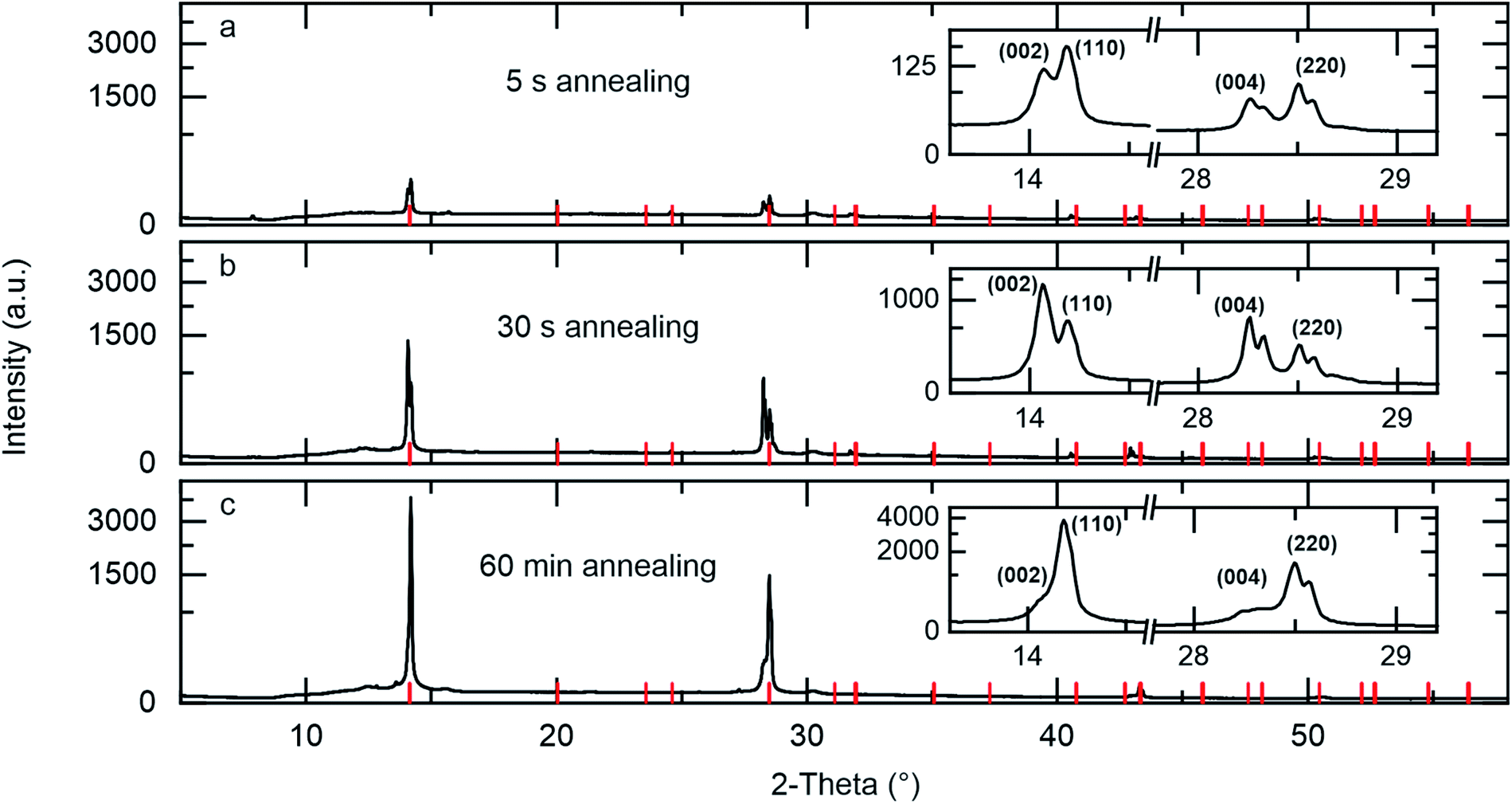 | ||
| Fig. 2 XRD data of MAPbI3 samples that were thermally annealed for (a) 5 s, (b) 30 s and (c) 60 min. After 5 s of annealing, no more precursor residues were found. The texture gradually changes from non-uniform with local (002) and (110) orientation to a prevailing (110) texture. | ||
Since the c-axis correlates with the direction of ferroelectric polarization in a tetragonal perovskite unit cell, we can conclude on the dominant ferroelectric polarization orientation from the XRD data.19 Yet, a more detailed and spatially resolved microscopic picture of the ferroelectric polarization can be gained using PFM. In contrast to XRD, PFM can monitor ferroelectric domains with high spatial resolution by detecting (alternating) piezoresponse which is correlated to the crystal polarization. The two predominant orientations of the c-axis, in-plane and out-of-plane, call for using lateral and vertical PFM in order to distinguish in-plane and out-of-plane polarization of the sample. Rows 2 and 3 of Fig. 1 depict the VPFM amplitudes and phases of samples 1–5. Rows 4 and 5 depict the corresponding LPFM amplitude and phase. In these PFM micrographs, every image pixel has a size of 13 × 13 nm2 allowing a detailed observation of domains.
Strikingly, but in accordance with the observed crystal texture, we found a gradual change of the ferroelectric polarization direction towards prolonged annealing times. On sample 1 with the shortest annealing time of 5 s, we find contrast in amplitude and phase of both VPFM and LPFM between individual small grains and their neighbors. While individual grains show uniform PFM amplitudes, which indicate a uniform polarization and orientation of each grain, the piezoresponse varies between different grains. In particular, we observed grains with both out-of-plane and in-plane polarization components, which is in accordance with the different grain orientations in sample 1 (XRD measurements, Fig. 2a). In addition, the various surface facets and surface potentials of curved grains with varying slopes may affect the PFM signal. After annealing for 30 s (sample 2), we observed large trapezoidal domains (bright areas in the VPFM amplitude) with an out-of-plane polarization component. On sample 3, which was annealed for 60 s, a similar domain configuration was created. As we will discuss in Section 2.3, the areas of low VPFM amplitude represent domains of in-plane polarization. After 3 min of annealing (sample 4), we observed a notably different domain pattern: while only a few grains exhibit trapezoidal domains with high VPFM amplitude, most grains possess clear domain features in LPFM, i.e., both LPFM amplitude and phase of sample 4 show striped domains with alternating polarization. On sample 5, which was annealed for 60 min, the VPFM contrast finally vanishes and a distinct LPFM contrast indicates an almost complete transformation to in-plane polarization direction. Both, PFM amplitude and phase, confirm striped domain patterns on each MAPbI3 grain of sample 5 that clearly differ in size and shape from the trapezoidal domains with out-of-plane polarization that were visible on samples 2 and 3. The enhanced LPFM amplitudes at domain walls of sample 5 might indicate 90°-domain configurations, where the polarization orientation of neighboring domains forms an angle of 90°.14 We finally note that neither the vertical domains with out-of-plane piezoresponse nor the lateral domains are visible in the topography. We can also exclude any topographic crosstalk as the origin of the domain contrast since the domains often appear to continue even across grain boundaries, changes in slope and curvature of grains.
Altogether, this set of measurements reveals that the annealing time influences the size of the grains as well as the size and the polarization orientation of the ferroelectric domains. Starting with small grain sizes and a random polarization orientation containing both out-of-plane and in-plane polarization components, the grain size increases during a short period of annealing. After 30–60 s of annealing, we find significant amounts of domains with out-of-plane polarization components. Prolonging the time of annealing further does not cause notable changes to the grain diameter, but transforms the polarization to a vastly predominant in-plane orientation.
Notably, we observed the domain features also with stiffer cantilevers, which reduce electrostatic contributions, but at the same time increase the sample wear. In general, the number of PFM measurements on the same sample position is limited by sample wear, requiring occasional sample replacements. This, however, does not affect the comparability of the samples and measurement results, since the qualitative observations were reproduced several times on identical samples.
We used this measurement of the contact potential difference (CPD) to reveal surface potential differences between vertical and lateral domains with high spatial resolution. Depending on the polarization orientation of an individual vertical domain, its surface potential is either higher or lower than that of the surrounding grain surface. Fig. 3 shows another sample that was thermally annealed for 60 s, producing similar features in topography (Fig. 3a) and VPFM amplitude (Fig. 3b) as sample 3 (Fig. 1). Fig. 3c and the sampling area magnification in Fig. 3d depict the CPD of the same sample position and reveal different surface potentials on the MAPbI3 grains. While many large grains possess high CPDs, most small grains possess lower CPDs, which might indicate a different grain orientation and hence different crystal facets, well agreeing to what we observed on sample 1 in Fig. 1.19,45 On the representative grains 1 and 2 in Fig. 3d, we observe a homogenously high CPD, but the trapezoidal domains with a high VPFM amplitude exhibit a reduced CPD. In Fig. 3e, the CPD line scan along the dashed line in Fig. 3d shows a local CPD reduction of about 50 mV, which correlates to the high local VPFM amplitude in Fig. 3b. In this KPFM measurement setup, a higher CPD corresponds to a higher absolute work function. Hence, we attribute this reduced CPD to an accumulation of negative surface charges, e.g. iodine ions or electrons, to compensate the polarization fields within the domains. We therefore conclude that the polarization vector points downwards (towards the substrate) in the two vertical domains of the investigated sample region. Throughout all samples, FM-KPFM measurements consistently show the same reduced CPD on all domains with high VPFM amplitude relative to other parts of the grains with low VPFM amplitude (further examples are provided in the ESI Fig. S2†).
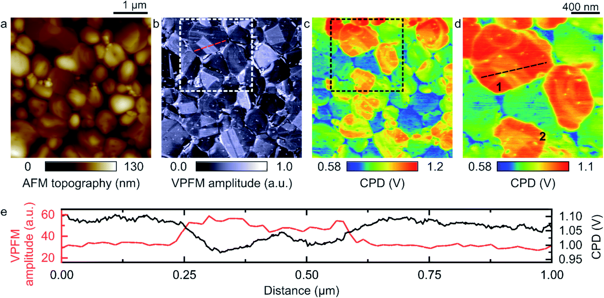 | ||
| Fig. 3 Modulation of the surface potential by ferroelectric domains with out-of-plane polarization components. (a) Topography and (b) VPFM amplitude of a representative MAPbI3 layer that was annealed for 60 s. Amidst the vast areas of low VPFM amplitude, some grains exhibit large domains that produce high VPFM amplitudes, attributable to local out-of-plane polarization components. (c) The FM-KPFM image of the same sample position shows a varying contact potential difference (CPD) between grains due to different grain orientations, but also due to a modulation of the CPD by domains with out-of-plane polarization. (d) From the enlarged sample area, the difference in CPD of about 50 mV can be deduced by comparing out-of-plane polarized domains and their surrounding area. The lower CPD on the domains with out-of-plane polarization indicates that the polarization vector points downwards. (e) Line scans along the dashed lines in b + d show differences in CPD of about 50 mV at vertical domains with increased VPFM amplitude. | ||
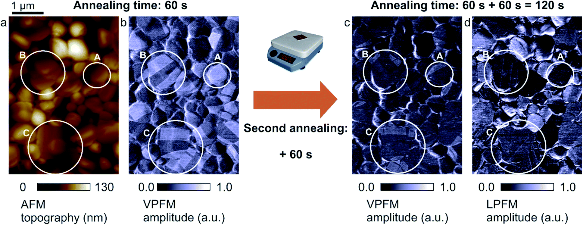 | ||
| Fig. 4 Ferroelectric domains before and after a second annealing step. (a) Sample topography. (b) The VPFM amplitude of a sample after the initial 60 s of annealing shows out-of-plane polarized domains. (c) After the second annealing for 60 s, the vertical domains shrink in size and partly vanish (marked in white). (d) At the same time, alternating domains with in-plane polarization occur in LPFM, displacing the vertical domains. | ||
The VPFM image in Fig. 4b highlights some domains with vertical polarization components: position A marks a grain with a relatively small diameter. Its homogenously high VPFM amplitude indicates a uniform vertical polarization throughout the grain. Positions B and C mark larger grains comprising domains of different polarization orientation, exhibiting alternating high- and low-amplitudes. After the second annealing, the shape of the grains and their topography persisted (ESI Fig. S3†), whereas the domain sizes and shapes changed significantly.
Fig. 4c shows that areas with low VPFM amplitude grow in size whereas domains with high amplitude shrink. For example, on the previously out-of-plane polarized, small grain at position A, two domains formed. Of these two domains, only the narrower domain at the top of the area exhibits high VPFM amplitude and hence vertical polarization (Fig. 4c). The larger domain exhibits only low VPFM amplitude. The domains at positions B and C seemingly migrate towards the grain boundaries, leaving behind areas of low VPFM amplitude. In these areas of low VPFM amplitude, small, needle-like domains emerge showing contrast in LPFM (Fig. 4d). Since these domains are neither visible in VPFM nor do correlate to topography features, we conclude that they possess in-plane polarization. These needle-shaped, in-plane polarized domains start to grow from the grain boundaries and spread over the grain, thus replacing domains of out-of-plane polarization with in-plane polarization (ESI Fig. S4†).
A more detailed view on the displacement of vertical domains by horizontal domains is provided in Fig. 5a–c, comparing topography, VPFM and LPFM of a typical sample that was annealed for 2 min (the corresponding VPFM and LPFM phase images can be found in the ESI Fig. S5†). In the areas of low VPFM amplitude, the LPFM amplitude shows lateral domains drawing through the sample. During the transformation process, the sample exhibits distinct features of both vertical and lateral domains. The area highlighted with dashed rectangles in Fig. 5a–c is magnified in Fig. 5d–f revealing another characteristic transformation feature: on the encircled grain, the VPFM amplitude in Fig. 5e is weak except for two domains that show the characteristic trapezoidal domain shape and distinct contrast stemming from an out-of-plane polarization. The domain wall of this vertical domain exhibits a zigzagged indentation. The origin of this indentation can be clearly identified in the LPFM image in Fig. 5f as a needle-shaped lateral domain. Similar to ferroelectric domains in BaTiO3,49 this lateral domain emerges near one of the grain boundaries and extends over the grain surface until it hits a vertical domain wall. The domain frustration at the point of contact leads to an needle-shaped convergence of the lateral domain and comes along with a clear indentation of the vertical domain wall. Notably, this single grain comprises three types of domains: besides domains with out-of-plane polarization, we find domains with two different in-plane polarization directions, which is another striking evidence for the ferroelectric nature of MAPbI3. We observed similar features at other sample positions as depicted in the ESI Fig. S6.†
 | ||
| Fig. 5 MAPbI3 grains exhibit both out-of-plane and in-plane polarized domains after 2 min of thermal annealing. (a) Topography, (b) VPFM and (c) LPFM images. (d–f) The magnifications show the displacement of out-of-plane polarized domains by in-plane polarized domains. On the marked grain, an indentation of an out-of-plane polarized domain by the tip of an in-plane polarized domain that grew from the grain boundary becomes visible. Hence, this individual grain exhibits three different polarization orientations: besides the out-of-plane polarized domains, two alternating in-plane polarization orientations are clearly distinguishable in VPFM and LPFM. | ||
Fig. 6 shows a direct comparison of the topography (a + c) and LPFM phase (b + d) of a representative sample before and after the second annealing step (the corresponding LPFM amplitude images are provided in ESI Fig. S7†). The LPFM phase image (Fig. 6b) before the second annealing reveals in-plane polarization on most grains, but with non-uniform domain patterns. At position I, the domains are needle-shaped as described in Section 2.3. At least one of these needle-shaped domains extends over the adjacent grain boundary, facing other lateral domains perpendicularly. At positions II and III, the domain patterns are confined to individual grains. While the domains at position II vary in width, the lamellar domains at position III are rather evenly distributed.
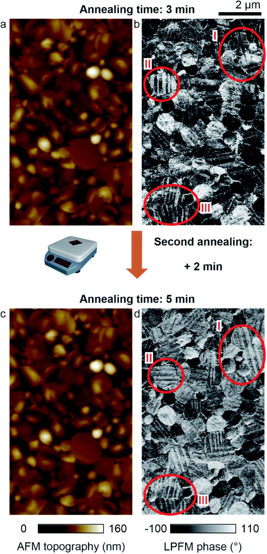 | ||
| Fig. 6 Formation of lateral domains with alternating in-plane polarization upon thermal annealing. (a) Topography of a representative MAPbI3 sample annealed for 3 min. (b) The LPFM phase shows striped domains. (c) Upon additional annealing for 2 min, the topography does not change, but some domains are strongly modified: (d) the LPFM phase image depicts domains that expand over grain boundaries (I), a rotation of domain patterns by 90° (II) or domains that retain their shapes, dimensions and positions (III). | ||
After the second annealing step of 2 min, some changes to the pattern of lateral domains become visible in the LPFM phase image in Fig. 6d. The initial needle-like domains at position I (Fig. 6b) grow and expand to uniformly alternating domains, notably extending over several grains (Fig. 6d). Moreover, we observed the formation of new lateral domain patterns, such as the replacement of domains and domain walls by perpendicular domains (positions I + II).
Both the formation of new domains and the modification of domains likely appear because of energetic optimization for both mechanical stress and electrostatic forces, similar to other ferroelectrics.9 Mediated by thermal annealing, this evolution of laterally polarized domains continues until a thermodynamically stable configuration of alternating domains is reached (sample 5, Fig. 1). At position III, the grain already exhibited a uniform domain pattern before the second annealing step. This domain pattern persisted after the second annealing. We note that the second annealing step for 2 min did not affect the topography (Fig. 6c).
From these observations, we conclude that the domains with vertical polarization may well influence the initial formation of lateral domains and their shapes. At a later stage, when these vertically polarized domains are extinct, we expect grain boundaries and crystal defects to control the formation of ferroelectric domains, as it is also known from other, inorganic perovskites.50,51 This interpretation is supported by a distinct angle of 45° between lateral domain walls and the grain boundaries (Fig. 5e and S4b†).22 Under the assumption that grain boundaries preferentially form along the (110) and (11*0) crystal planes in MAPbI3 (i.e. the basic planes of the MA-cation), this angle would signify lateral domain walls forming along the [100] and [010] directions.22
The reappearance of domain walls at position III upon heating above TC and subsequently cooling down below TC indicates an already energetically stable configuration, but also pinning at crystal defects and grain boundaries as well as clamping due to lateral stress. The latter may either originate from defect “healing”52 within the grains due to annealing or could stem from uniaxial forces exerted by neighboring grains.53,54 In polycrystalline thin-films, mechanical stress is a generic feature that occurs during grain growth and the formation of thin-films.34 Consequently, stress induced pinning may suppress domain modifications and hence force lattice distortions.19,54
Our study reveals that the annealing procedure acts as a driving force for the transformation of ferroelectric domains. During annealing the aspect ratio of grains changes significantly: grains grow to lateral diameters of several microns while their thickness remains constant at 300 nm. Initially, several polarization orientations coexist but mainly in-plane polarization remains after extended annealing. The domains evolve in MAPbI3 thin-films until stable domain patterns of alternating in-plane polarization exist. Once the polarization was switched to in-plane orientation, in our study, annealing has never triggered reappearance of any vertical domains.
2.2 Correlation of ferroelectric domain polarization and solar cell properties
To date, the extent to which ferroelectric domains influence the solar cell performance remains yet to be investigated, since a fundamental understanding of ferroelectric domain formation had been missing. With the toolbox above that allows the targeted formation of domains with in-plane and out-of-plane polarization, we now have the experimental means to correlate the domain polarization and the performance of MAPbI3 solar cells. For this study, we fabricated solar cells comprising polycrystalline MAPbI3 layers that were deposited as described above. One set of solar cells was annealed for 30 s, after which the MAI/PbI2-to-MAPbI3 conversion process was completed, and another set of samples was annealed for 60 min right after MAPbI3 deposition, both producing reproducible domain patterns. The former set exhibits notable out-of-plane domain polarization, the latter predominant in-plane domain polarization. To complete the solar cells, transport layers of [6,6]-phenyl C71-butyric acid methyl ester (PC71BM) and bathocuproine (BCP) were deposited from solution and a silver top electrode was sublimed in high vacuum. After the deposition of the perovskite layer, the solar cells were not annealed anymore to ensure stable domain configurations. During vacuum sublimation of the silver electrode, the device temperature did not exceed 40 °C and hence remained well below TC.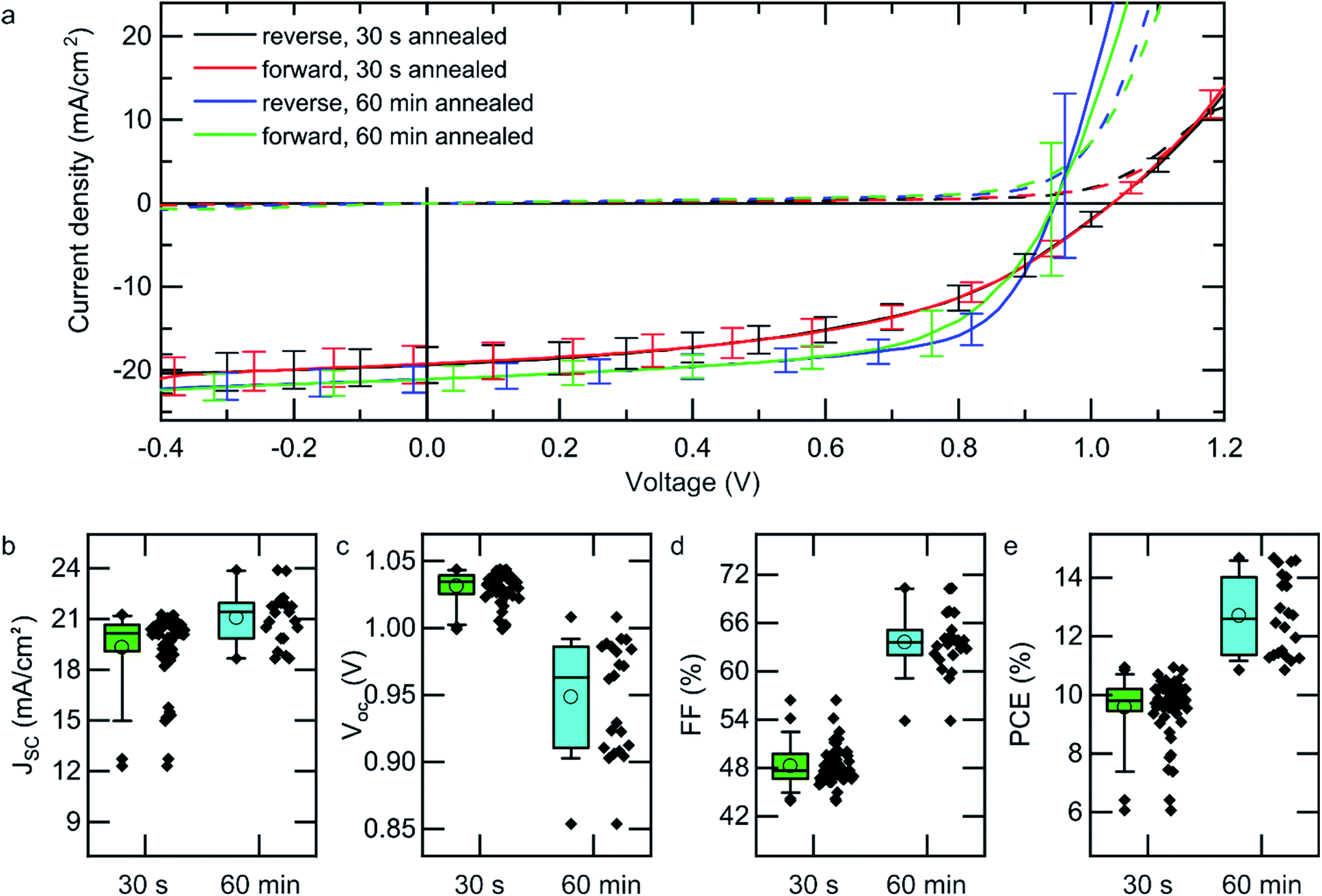 | ||
| Fig. 7 Solar cell performance in dependence of the perovskite layer annealing time. (a) Averaged J–V curves of solar cells comprising MAPbI3 thin-films that were annealed for 30 s during fabrication. These solar cells show reduced fill factors but higher VOC in comparison to solar cells comprising MAPbI3 thin-films that were annealed for 60 min. (Dashed lines represent dark curves of the solar cells.) (b–e) Characteristic solar cell parameters extracted from reverse and forward J–V scans. | ||
The black and red curves represent the backward and forward sweeps of 26 solar cells comprising MAPbI3 layers that were annealed for 30 s and exhibit large domains with out-of-plane polarization as exemplified in ESI Fig. S8.† The blue and green curves correspond to 11 solar cells with MAPbI3 layers that were thermally annealed for 60 min and possess striped lateral domains. Strikingly, the two sets of solar cells exhibit significantly different fill factors (FFs) and hence device performance: while solar cells with out-of-plane polarization components exhibit lower performance (average FF < 50%, PCE = 10%), the solar cells with alternating in-plane polarized domains possess average FF = 65% (Fig. 7d) and power conversion efficiencies (PCEs) of 13% (see Fig. 7e).
Notably, the influence of the domain polarization on the solar cell performance may be overlaid by other microstructural contributions such as grain growth during ongoing annealing and a concomitant change of grain boundary densities and defect states.57–59 Although these effects are partly difficult to disentangle experimentally, our observations very much resemble earlier theoretical studies on the influence of ferroelectric polarization on the solar cell performance.12 It was predicted that domains with alternating in-plane polarizations and their concomitant electrical fields assist with the spatial separation of charges and produce pathways for electrons and holes to the respective electrodes.11,12 Consequently, Shockley–Read–Hall recombination could be reduced, which in turn would improve the PCE of the solar cell due to an enhanced fill factor.12 Likewise, these simulations predicted that any out-of-plane polarization would not contribute to an improvement in the solar cell performance, producing only moderate efficiencies. Other earlier experimental works have reported that the performance of optimized solar cells decreases upon heating to above TC,60 where ferroelectric domains would usually disappear. The roles of ionic charges in the formation of domains has been discussed in our earlier work.22
In addition, we observe an average open-circuit voltage VOC = 1031 ± 11 mV in the set of solar cells with out-of-plane polarization, which is 80 mV higher than the VOC of solar cells comprising domains with in-plane polarization (VOC = 948 ± 42 mV). Interestingly, this difference in VOC is close to the 50 mV difference of the CPD between surfaces of domains with out-of-plane polarization and surfaces of domains with no out-of-plane polarization, which we discussed in Section 2.2. In light of the KPFM measurements in Section 2.2, we conclude that the VOC is modified not only by diverse crystal facets that modify the interface between MAPbI3 and the charge carrier transport layers,61,62 but also by the screening surface charges of the vertical ferroelectric domains.
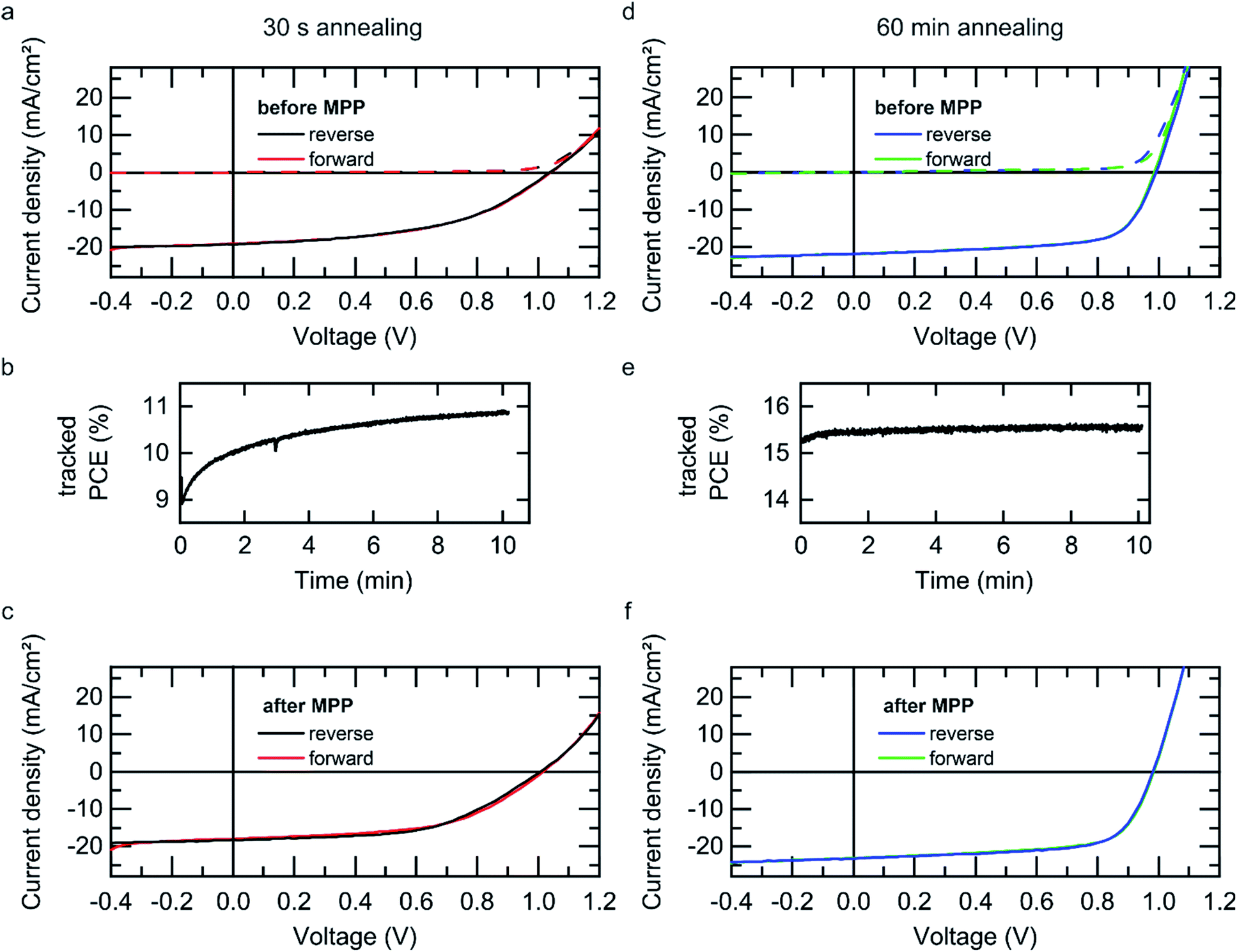 | ||
| Fig. 8 MPP tracking under 1 sun illumination. (a) Initial J–V curves of a solar cell that was annealed for 30 s. (b) The PCE increases significantly during MPP measurement. (c) After MPP-tracking, the J–V curves of the solar cell revert back to their initial shape. (d–f) After 60 min of thermal annealing, the PCE of a solar cell remains constant during MPP-tracking and the J–V curves persisted. | ||
Remarkably, 35 s after discontinuation of the 10 min of MPP tracking, the J–V curves of the solar cell in Fig. 8c reverted to about their initial shape. Only after extending the MPP tracking to 60 min, the changed J–V curves and hence the improved PCE persisted (ESI Fig. S9†) showing reduced VOC, and an enhanced fill factor. Notably, both types of solar cells in Fig. 8 show low hysteresis before and after MPP tracking which may indicate that ionic effects play a secondary role here. According to our experiments described above, the improvement of the PCE during MPP-tracking may well have its origin in a change of polarization orientation. Within the first 10 min of the experiment, the changes of the polarization direction may be rather small, and hence it reverts to its original orientation after discontinuation of the MPP tracking, e.g. mediated by pinning at defects or layer interfaces. A gradual increase of the polarization modulation for a longer period of MPP tracking may eventually bring the sample into a new equilibrium state from where the reverse process appears energetically unfavorable. The activation energy to overcome this tipping point may well stem from sample heating by illumination or from the electrical energy supply. Although this interpretation appears logical in light of the previous experiments, notably, tracking the change in polarization orientation is impossible with the experimental methods used here, as the top metal electrode conceals the sample region of interest. Removing the electrode or cleaving the sample would very likely result in mechanical strain that, by itself, can change the polarization orientation.
3 Conclusions
Our experimental study demonstrates how ferroelectric domains evolve upon thermal annealing, which is a common fabrication step of MAPbI3 solar cells. Within seconds to minutes, thermal annealing of MAPbI3 thin-films triggers the transformation of coexisting out-of-plane and in-plane polarizations towards a predominant in-plane polarization. We tracked this transformation by studying distinct contrasts in VPFM and LPFM imaging. During this transformation, we occasionally observed at least three different polarization orientations within individual grains, supporting the case for ferroelectricity of MAPbI3. Vertical polarization components modulate the surface potential (CPD) in order to compensate internal electrical fields as visible in FM-KPFM.In recent years, many reports focused on the influence of the manufacturing processes of OMH perovskite thin-films on the performance of solar cells. In particular, the layers underneath,63,64 additives to the precursor solutions,65–67 solvent vapor annealing,55,68,69 variations of the annealing temperature38,70 and the annealing duration71 have been reported to affect the thin-film formation and to determine the power conversion efficiency. The correlation of ferroelectric domain polarization and device performance in this work suggests that the configuration and evolution of ferroelectric domains should be considered as an additional critical mechanism affecting solar cell characteristics. Solar cells with alternating lateral domains comprise best fill factors and efficiencies, whereas solar cells with shortly-annealed MAPbI3 thin-films and vertical domains exhibit only moderate performance. Not least, solar cells with out-of-plane polarization presented themselves less stable during electrical characterization. This observation is critically important for any type of J–V measurements or in particular MPP-tracking. Notably, intrinsic conductivity, photoconductivity and ionic conductivity also change during thermal annealing and hence may also affect the solar cell properties. While it is difficult, if not impossible, to disentangle these effects, the agreement of this experimental study with earlier theoretic discussions and drift-diffusion modeling within ferroelectric domain assemblies is intriguing.12
4 Experimental
4.1 Sample fabrication
The polycrystalline MAPbI3 thin-films were fabricated following our earlier works and characterized under inert atmosphere.14,19 The indium tin oxide (ITO) coated substrates were cleaned with acetone and isopropanol in an ultrasonic bath, after which they were exposed to an oxygen plasma for 2 min and transferred into a glovebox. Poly(3,4-ethylenedioxythiophene):poly(4-styrenesulphonate) (PEDOT:PSS, VPAI 4083, Heraeus Clevios, diluted with ethanol 1![[thin space (1/6-em)]](https://www.rsc.org/images/entities/char_2009.gif) :3 v/v) was blade-coated (Zehntner ZUA-2000) atop the ITO, and the substrates were thermally annealed for 10 min at 140 °C. Lead iodide (PbI2, Sigma Aldrich or Alfa Aesar (sample 5, Fig. 1); both PbI2 yield the same grain sizes and domain patterns, ESI Fig. S10†) was dissolved in dimethyl sulfoxide (DMSO, 250 mg mL−1) and 1-chloronaphthalene was added to the solution (100:1 v/v). Then, the PbI2 solution was blade-coated onto the PEDOT:PSS layer (4 mm s−1, at 60 °C, gap 70 μm) and quenched with a nitrogen stream. In a second step, a solution of methylammonium iodide (MAI, Lumtec Ltd.) and methylammonium chloride (MACl, MAI:MACl 9:1 wt/wt, in isopropanol 40 g L−1) was spin cast (1350 rpm) to convert the precursors into a 300 nm MAPbI3 thin-film. All samples were initially annealed (100 °C, 5 s) to warrant a complete and rapid conversion into perovskite structure. Any further annealing as described above was accomplished under Petri dishes (volume approx. 5 cm3) for the specified annealing durations. To fabricate solar cells, the samples were completed by spin casting layers of [6,6]-phenyl C71-butyric acid methyl ester (PC71BM in chlorobenzene) and bathocuproine (BCP in ethanol) on top of MAPbI3. A silver top electrode was sublimed in high vacuum.
:3 v/v) was blade-coated (Zehntner ZUA-2000) atop the ITO, and the substrates were thermally annealed for 10 min at 140 °C. Lead iodide (PbI2, Sigma Aldrich or Alfa Aesar (sample 5, Fig. 1); both PbI2 yield the same grain sizes and domain patterns, ESI Fig. S10†) was dissolved in dimethyl sulfoxide (DMSO, 250 mg mL−1) and 1-chloronaphthalene was added to the solution (100:1 v/v). Then, the PbI2 solution was blade-coated onto the PEDOT:PSS layer (4 mm s−1, at 60 °C, gap 70 μm) and quenched with a nitrogen stream. In a second step, a solution of methylammonium iodide (MAI, Lumtec Ltd.) and methylammonium chloride (MACl, MAI:MACl 9:1 wt/wt, in isopropanol 40 g L−1) was spin cast (1350 rpm) to convert the precursors into a 300 nm MAPbI3 thin-film. All samples were initially annealed (100 °C, 5 s) to warrant a complete and rapid conversion into perovskite structure. Any further annealing as described above was accomplished under Petri dishes (volume approx. 5 cm3) for the specified annealing durations. To fabricate solar cells, the samples were completed by spin casting layers of [6,6]-phenyl C71-butyric acid methyl ester (PC71BM in chlorobenzene) and bathocuproine (BCP in ethanol) on top of MAPbI3. A silver top electrode was sublimed in high vacuum.
4.2 Annealing conditions
Fig. 1: sample 1: 5 s no Petri dish; samples 2, 3, 4 and 5: 30 s, 60 s, 3 min, 60 min with Petri dish. Fig. 2: (a) 5 s no Petri dish; (b) 30 s with Petri dish, (c) 60 min with Petri dish. Fig. 3: 5 s and then 60 s with Petri dish. Fig. 4: (a + b) 5 s and then 60 s with Petri dish; (c + d) additional annealing for 60 s with Petri dish (total annealing: 120 s). Fig. 5: 5 s and then 2 min with Petri dish. Fig. 6: (a + b) 5 s and then 3 min with Petri dish; (c + d) additional annealing for 2 min with Petri dish (total annealing: 5 min). Fig. 7 and 8: annealing like samples 2 and 5 in Fig. 1.4.3 Atomic force microscopy
The atomic force microscopy (AFM) measurements were performed on a Dimension Icon (Bruker) under nitrogen atmosphere with platinum-iridium coated conductive tips (SCM-PIC, spring constant k = 0.1 N m−1). In order to enhance the resolution and reduce the signal-to-noise ratio, contact resonance amplification was used for VPFM and LPFM, and the driving AC frequencies were set a few kHz below the respective contact resonance. Forces in the range of 3–10 nN and moderate AC-bias amplitudes of 1000–1500 mV were applied in order to minimize damages to the thin-film samples and enable repetitive measurements of several PFM micrographs at the same sample position. The PFM amplitude and phase scales were chosen for optimal contrast. The contact resonance enhancement impedes a reliable absolute calibration of the PFM data, and the scale bars were therefore set to arbitrary units for both LPFM and VPFM amplitudes. For FM-KPFM, platinum-iridium coated tips (SCM-PIT-V2, spring constant k = 3 N m−1) and a drive amplitude of 3000 mV were used. All PFM and KPFM scans were conducted in the dark without additional DC biases.4.4 Optoelectronic characterization
The current density–voltage (J–V) curves of the solar cells were measured in inert atmosphere with a Keithley source measurement unit in the dark and under illumination from a solar simulator (Sciencetech Lightline, AM 1.5, 1000 W m−2, calibrated with a Si reference solar cell). The scan speed in reverse (1.2 V → −0.4 V) and forward (−0.4 V → 1.2 V) direction was 100 mV s−1. During MPP tracking, the voltage was held for 300 ms and the PCE was calculated from the respective current. The J–V curves were measured again 30–60 s after completion of the MPP tracking.4.5 X-ray diffraction
Powder diffraction data were collected on a D8 Advance (Bruker AXS) equipped with an energy discriminating LYNXEYE XE-T 1D detector using Cu Kα radiation in a θ–2θ scan in the range from 5° to 60° 2θ with a step size of 0.010° and measurement time of 4 s per step. Due to their sensitivity to oxygen and moisture, the samples were packed into a sealed sample holder inside a glove box under nitrogen atmosphere, and instantly measured after unloading. The texture axis was assumed to be perpendicular to the surface of the sample, permitting the use of sample rotation (30° s−1) to reduce the effects of particle counting statistics.Author contributions
T. L., H. R. and A. C. have conceived the experiments and jointly written the manuscript. T. L. and H. R. have carried out the experiments. F. A. has contributed the XRD measurements and their interpretation. M. J. H. has advised on data interpretation and ferroelectric properties. A. C. has supervised the work. All authors have discussed the data and approved the manuscript.Conflicts of interest
There are no conflicts to declare.Acknowledgements
The authors acknowledge funding by the Carl Zeiss Foundation (project KeraSolar) and support by the Helmholtz Programme “Science and Technology of Nanosystems” (STN). T. L. acknowledges funding by the Landesgraduiertenförderung Baden-Württemberg. We thank Simon Petrick for performing the grain size analysis and Alexander D. Schulz for fruitful discussions.References
- M. A. Green, E. D. Dunlop, J. Hohl-Ebinger, M. Yoshita, N. Kopidakis and A. W. Y. Ho-Baillie, Prog. Photovoltaics, 2020, 28, 3–15 Search PubMed.
- C. Wehrenfennig, G. E. Eperon, M. B. Johnston, H. J. Snaith and L. M. Herz, Adv. Mater., 2014, 26, 1584–1589 CrossRef CAS PubMed.
- L. M. Herz, ACS Energy Lett., 2017, 2, 1539–1548 CrossRef CAS.
- J. M. Frost, K. T. Butler and A. Walsh, APL Mater., 2014, 2, 081506 CrossRef.
- A. M. A. Leguy, J. M. Frost, A. P. McMahon, V. G. Sakai, W. Kockelmann, C. Law, X. Li, F. Foglia, A. Walsh, B. C. O'Regan, J. Nelson, J. T. Cabral and P. R. F. Barnes, Nat. Commun., 2015, 6, 7124 CrossRef PubMed.
- A. Stroppa, C. Quarti, F. De Angelis and S. Picozzi, J. Phys. Chem. Lett., 2015, 6(12), 2223–2231 CrossRef CAS PubMed.
- M. E. Lines and A. M. Glass, Principles and Applications of Ferroelectrics and Related Materials, Oxford University Press, Oxford, 1977 Search PubMed.
- B. Jaffe, W. R. Cook Jr and H. Jaffe, Piezoelectric Ceramics, Academic Press, London, 1971 Search PubMed.
- D. Damjanovic, Rep. Prog. Phys., 1998, 61, 1267 CrossRef CAS.
- J. M. Frost, K. T. Butler, F. Brivio, C. H. Hendon, M. van Schilfgaarde and A. Walsh, Nano Lett., 2014, 14(5), 2584–2590 CrossRef CAS PubMed.
- T. S. Sherkar and L. J. A. Koster, Phys. Chem. Chem. Phys., 2016, 18, 331 RSC.
- D. Rossi, A. Pecchia, M. Auf der Maur, T. Leonhard, H. Röhm, M. J. Hoffmann, A. Colsmann and A. Di Carlo, Nano Energy, 2018, 48, 20–26 CrossRef CAS.
- I. M. Hermes, S. A. Bretschneider, V. W. Bergmann, D. Li, A. Klasen, J. Mars, W. Tremel, F. Laquai, H.-J. Butt, M. Mezger, R. Berger, B. J. Rodriguez and S. A. L. Weber, J. Phys. Chem. C, 2016, 120, 5724–5731 CrossRef CAS.
- H. Röhm, T. Leonhard, M. J. Hoffmann and A. Colsmann, Energy Environ. Sci., 2017, 10, 950 RSC.
- C. Harnagea, A. Pignolet, M. Alexe and D. Hesse, Integr. Ferroelectr., 2004, 60, 101–110 CrossRef CAS.
- L. Collins, Y. Liu, O. S. Ovchinnikova and R. Proksch, ACS Nano, 2019, 13(7), 8055–8066 CrossRef CAS PubMed.
- R. K. Vasudevan, N. Balke, P. Maksymovych, S. Jesse and S. V. Kalinin, Appl. Phys. Rev., 2017, 4, 021302 Search PubMed.
- C. Eames, J. M. Frost, P. R. F. Barnes, B. C. O'Regan, A. Walsh and M. S. Islam, Nat. Commun., 2015, 6, 7497 CrossRef CAS PubMed.
- T. Leonhard, A. D. Schulz, H. Röhm, S. Wagner, F. J. Altermann, W. Rheinheimer, M. J. Hoffmann and A. Colsmann, Energy Technol., 2019, 7, 1800989 CrossRef.
- H. Röhm, T. Leonhard, A. D. Schulz, S. Wagner, M. J. Hoffmann and A. Colsmann, Adv. Mater., 2019, 31, 1806661 CrossRef PubMed.
- J. Breternitz, F. Lehmann, S. A. Barnett, H. Nowell and S. Schorr, Angew. Chem., 2020, 132, 432–436 CrossRef.
- H. Röhm, T. Leonhard, M. J. Hoffmann and A. Colsmann, Adv. Funct. Mater., 2020, 30, 1908657 CrossRef.
- Y. Rakita, O. Bar-Elli, E. Meirzadeh, H. Kaslasi, Y. Peleg, G. Hodes, I. Lubomirsky, D. Oron, D. Ehre and D. Cahen, Proc. Natl. Acad. Sci. U. S. A., 2017, 114(28), E5504–E5512 CrossRef CAS PubMed.
- Z. Fan, J. Xiao, K. Sun, L. Chen, Y. Hu, J. Ouyang, K. P. Ong, K. Zeng and J. Wang, J. Phys. Chem. Lett., 2015, 6, 1155–1161 CrossRef CAS PubMed.
- W. T. H. Koch, R. Munser, W. Ruppel and P. Würfel, Solid State Commun., 1975, 17(7), 847–850 CrossRef CAS.
- R. von Baltz and W. Kraut, Phys. Rev. B: Condens. Matter Mater. Phys., 1981, 23(10), 5590–5596 CrossRef CAS.
- E. Strelcov, Q. Dong, T. Li, J. Chae, Y. Shao, Y. Deng, A. Gruverman, J. Huang and A. Centrone, Sci. Adv., 2017, 3, e1602165 CrossRef PubMed.
- G. A. MacDonald, C. M. Heveran, M. Yang, D. Moore, K. Zhu, V. L. Ferguson, J. P. Killgore and F. W. DelRio, ACS Appl. Mater. Interfaces, 2017, 9, 33565–33570 CrossRef CAS PubMed.
- Y. Liu, L. Collins, R. Proksch, S. Kim, B. R. Watson, B. Doughty, T. R. Calhoun, M. Ahmadi, A. V. Ievlev, S. Jesse, S. T. Retterer, A. Belianinov, K. Xiao, J. Huang, B. G. Sumpter, S. V. Kalinin, B. Hu and O. S. Ovchinnikova, Nat. Mater., 2018, 17, 1013–1019 CrossRef CAS PubMed.
- I. M. Hermes, A. Best, L. Winkelmann, J. Mars, S. M. Vorpahl, M. Mezger, L. Collins, H.-J. Butt, D. S. Ginger, K. Koynov and S. A. L. Weber, Energy Environ. Sci., 2020, 13, 4168–4177 RSC.
- S. M. Vorpahl, R. Giridharagopal, G. E. Eperon, I. M. Hermes, S. A. L. Weber and D. S. Ginger, ACS Appl. Energy Mater., 2018, 1, 1534–1539 CrossRef CAS.
- B. Huang, G. Kong, E. N. Esfahani, S. Chen, Q. Li, J. Yu, N. Xu, Y. Zhang, S. Xie, H. Wen, P. Gao, J. Zhao and J. Li, npj Quantum Mater., 2018, 3, 30 CrossRef.
- A. D. Schulz, H. Röhm, T. Leonhard, S. Wagner, M. J. Hoffmann and A. Colsmann, Nat. Mater., 2019, 18, 1050 CrossRef CAS PubMed.
- G. Arlt, Ferroelectrics, 1990, 104(1), 217–227 CrossRef CAS.
- A. Poglitsch and D. Weber, J. Chem. Phys., 1987, 87, 11 CrossRef.
- Z. Xiao, C. Bi, Y. Shao, Q. Dong, Q. Wang, Y. Yuan, C. Wang, Y. Gao and J. Huang, Energy Environ. Sci., 2014, 7, 2619 RSC.
- C. Bi, Y. Shao, Y. Yuan, Z. Xiao, C. Wang, Y. Gao and J. Huang, J. Mater. Chem. A, 2014, 2, 18508 RSC.
- W. Nie, H. Tsai, R. Asadpour, J.-C. Blancon, A. J. Neukirch, G. Gupta, J. J. Crochet, M. Chhowalla, S. Tretiak, M. A. Alam, H.-L. Wang and A. D. Mohite, Science, 2015, 347(6221), 522–525 CrossRef CAS PubMed.
- M. Ralaiarisoa, Y. Busby, J. Frisch, I. Salzmann, J.-J. Pireaux and N. Koch, Phys. Chem. Chem. Phys., 2017, 19, 828 RSC.
- N. J. Jeon, J. H. Noh, Y. C. Kim, W. S. Yang, S. Ryu and S. I. Seok, Nat. Mater., 2014, 13, 897–903 CrossRef CAS PubMed.
- M. Saliba, J.-P. Correa-Baena, C. M. Wolff, M. Stolterfoht, N. Phung, S. Albrecht, D. Neher and A. Abate, Chem. Mater., 2018, 30, 4193–4201 CrossRef CAS.
- A. Gruverman, M. Alexe and D. Meier, Nat. Commun., 2019, 10, 1661 CrossRef PubMed.
- E. Soergel, J. Phys. D: Appl. Phys., 2011, 44, 464003 CrossRef.
- S. V Kalinin, Y. Kim, D. D Fong and A. N. Morozovska, Rep. Prog. Phys., 2018, 81, 036502 CrossRef PubMed.
- S. Sadewasser, T. Glatzel, M. Rusu, A. Jäger-Waldau and M. C. Lux-Steiner, Appl. Phys. Lett., 2002, 80, 2979 CrossRef CAS.
- R. C. Bradt and G. S. Ansell, J. Am. Ceram. Soc., 1969, 52, 192–198 CrossRef CAS.
- W. A. Schulze and K. Ogino, Ferroelectrics, 1988, 87, 361–377 CrossRef.
- I. S. Zheludev, Domain Structure of Ferroelectrics and Antiferroelectrics, in Physics of Crystalline Dielectrics, Springer, Boston, 1971 Search PubMed.
- A. Hershkovitz, F. Johann, M. Barzilay, A. H. Avidor and Y. Ivry, Acta Mater., 2020, 187, 186–190 CrossRef CAS.
- P. V. Lambeck and G. H. Jonker, Ferroelectrics, 1978, 22, 729–731 CrossRef CAS.
- B. J. Rodriguez, Y. H. Chu, R. Ramesh and S. V. Kalinin, Appl. Phys. Lett., 2008, 93, 142901 CrossRef.
- F. Wang, S. Bai, W. Tress, A. Hagfeldt and F. Gao, npj Flexible Electron., 2018, 2, 22 CrossRef.
- G. Arlt, J. Mater. Sci., 1990, 25, 2655–2666 CrossRef CAS.
- S. Jariwala, H. Sun, G. W. P. Adhyaksa, A. Lof, L. A. Muscarella, B. Ehrler, E. C. Garnett and D. S. Ginger, Joule, 2019, 3(12), 3048–3060 CrossRef CAS.
- Z. Xiao, Q. Dong, C. Bi, Y. Shao, Y. Yuan and J. Huang, Adv.Mater., 2014, 26, 6503–6509 CrossRef CAS PubMed.
- P. Fassl, V. Lami, A. Bausch, Z. Wang, M. T. Klug, H. J. Snaith and Y. Vaynzof, Energy Environ. Sci., 2018, 11, 3380 RSC.
- G. W. P. Adhyaksa, S. Brittman, H. Abolins, A. Lof, X. Li, J. D. Keelor, Y. Luo, T. Duevski, R. M. A. Heeren, S. R. Ellis, D. P. Fenning and E. C. Garnett, Adv. Mater., 2018, 30, 1804792 CrossRef PubMed.
- R. Ciesielski, F. Schäfer, N. F. Hartmann, N. Giesbrecht, T. Bein, P. Docampo and A. Hartschuh, ACS Appl. Mater. Interfaces, 2018, 10, 7974–7981 CrossRef CAS PubMed.
- N. Phung, A. Al-Ashouri, S. Meloni, A. Mattoni, S. Albrecht, E. L. Unger, A. Merdasa and A. Abate, Adv. Energy Mater., 2020, 10, 1903735 CrossRef CAS.
- J. A. Schwenzer, L. Rakocevic, R. Gehlhaar, T. Abzieher, S. Gharibzadeh, S. Moghadamzadeh, A. Quintilla, B. S. Richards, U. Lemmer and U. W. Paetzold, ACS Appl. Mater. Interfaces, 2018, 10(19), 16390–16399 CrossRef CAS PubMed.
- S. A. L. Weber, I. M. Hermes, S.-H. Turren-Cruz, C. Gort, V. W. Bergmann, L. Gilson, A. Hagfeldt, M. Graetzel, W. Tress and R. Berger, Energy Environ. Sci., 2018, 11, 2404 RSC.
- S. Y. Leblebici, L. Leppert, Y. Li, S. E. Reyes-Lillo, S. Wickenburg, E. Wong, J. Lee, M. Melli, D. Ziegler, D. K. Angell, D. F. Ogletree, P. D. Ashby, F. M. Toma, J. B. Neaton, I. D. Sharp and A. Weber-Bargioni, Nat. Energy, 2016, 1, 16093 CrossRef CAS.
- E. M. Miller, Y. Zhao, C. C. Mercado, S. K. Saha, J. M. Luther, K. Zhu, V. Stevanović, C. L. Perkins and J. van de Lagemaat, Phys. Chem. Chem. Phys., 2014, 16, 22122–22130 RSC.
- C. Bi, Q. Wang, Y. Shao, Y. Yuan, Z. Xiao and J. Huang, Nat. Commun., 2015, 6, 7747 CrossRef CAS PubMed.
- Y.-J. Jeon, S. Lee, R. Kang, J.-E. Kim, J.-S. Yeo, S.-H. Lee, S.-S. Kim, J.-M. Yun and D.-Y. Kim, Sci. Rep., 2014, 4, 6953 CrossRef CAS PubMed.
- B. Lee, T. Hwang, S. Lee, B. Shin and B. Park, Sci. Rep., 2019, 9, 4803 CrossRef PubMed.
- X. Zheng, Y. Hou, C. Bao, J. Yin, F. Yuan, Z. Huang, K. Song, J. Liu, J. Troughton, N. Gasparini, C. Zhou, Y. Lin, D.-J. Xue, B. Chen, A. K. Johnston, N. Wei, M. N. Hedhili, M. Wei, A. Y. Alsalloum, P. Maity, B. Turedi, C. Yang, D. Baran, T. D. Anthopoulos, Y. Han, Z.-H. Lu, O. F. Mohammed, F. Gao, E. H. Sargent and O. M. Bakr, Nat. Energy, 2020, 5, 131–140 CrossRef CAS.
- J. Liu, C. Gao, X. He, Q. Ye, L. Ouyang, D. Zhuang, C. Liao, J. Mei and W. Lau, ACS Appl. Mater. Interfaces, 2015, 7(43), 24008–24015 CrossRef CAS PubMed.
- Q. Liang, J. Liu, Z. Cheng, Y. Li, L. Chen, R. Zhang, J. Zhang and Y. Han, J. Mater. Chem. A, 2016, 4, 223 RSC.
- A. Dualeh, N. Tétreault, T. Moehl, P. Gao, M. K. Nazeeruddin and M. Grätzel, Adv. Funct. Mater., 2014, 24, 3250–3258 CrossRef CAS.
- L. Huang, Z. Hu, G. Yue, J. Liu, X. Cui, J. Zhang and Y. Zhu, Phys. Chem. Chem. Phys., 2015, 17, 22015 RSC.
Footnote |
| † Electronic supplementary information (ESI) available. See DOI: 10.1039/d1ta06290e |
| This journal is © The Royal Society of Chemistry 2021 |