
A theoretical study of Lifshitz transition for 2H-TaS2†
Wenxuan
Wang
a,
Zhenyi
Jiang
 *a,
Xiaodong
Zhang
*a,
Jiming
Zheng
a,
Hongwei
Du
a and
Zhiyong
Zhang
b
*a,
Xiaodong
Zhang
*a,
Jiming
Zheng
a,
Hongwei
Du
a and
Zhiyong
Zhang
b
aShaanxi Key Laboratory for Theoretical Physics Frontiers, Institute of Modern Physics, Northwest University, Xi’an 710069, China
bStanford Research Computing Center, Stanford University, Stanford, CA 94305, USA
First published on 11th May 2024
Abstract
Lifshitz transition was proposed to explain a change of the topology structure in a Fermi surface induced by continuous lattice deformation without symmetry breaking since 1960. It is well known that the anomalies of the kinetic coefficients (the coefficient of heat conduction and electrical conductivity, viscosity, sound absorption, etc.) are usually closely connected with the Lifshitz transition behavior. 2H-TaS2 is a typical representative to study its anomalies of temperature dependence of heat capacity, resistivity, Hall effect, and magnetic susceptibility. Its geometrical structure of the charge density wave (CDW) phase and layer number dependence of carrier-sign alternation upon cooling in the Hall measurements have not been well understood. The geometrical structure (T–Ts) of the CDW phase was predicted through first principles calculations for bulk and mono-layer 2H-TaS2. Driven by electron-lattice coupling, Ta atoms contract to form a partially gapped CDW phase. The CDW phase has a larger average interlayer separation of S–S atoms in the adjacent two layers compared with the metal phase, which results in a weaker chemical bonding among S–S atoms in the adjacent two layers and then a narrower bandwidth of the energy band. The narrower bandwidth of the energy band leads to a larger density of states (DOS) in the out-of-plane direction above the Fermi level for the CDW phase. As the Fermi level continually drops from the DOS region with a negative slope to that with a positive slope on cooling, the reversal of the p → n type carrier and the pocket-vanishing-type Lifshitz transition occur in the bulk 2H-TaS2. However, the Fermi level slightly drops by 6 meV and happens to be at the positions of pseudo band gaps, so the reduction of in-plane DOS and total DOS is responsible for the always p-type carrier in the mono-layer samples. Our CDW vector of the k-space separation between two saddle points is QSP ≈ 0.62 GK and can provide a theoretical support for the “saddle-point” CDW mechanism proposed by Rice and Scott. Our theoretical explanation gives a new understanding of both Lifshitz transition for symmetry breaking and reversal for the p–n carrier sign in the Hall measurements in various two-dimensional transition metal disulfides.
1. Introduction
Half a century ago, Lifshitz considered an electronic phase transition (PT) associated with a change in the Fermi surface topology induced by continuous lattice deformation for noninteracting fermions.1 This electronic PT, now called the Lifshitz transition, is unique in the sense that it is not associated with structural symmetry breaking. Lifshitz gave two types of changes in the Fermi surface topology: one is associated with the collapse of a cylindrical Fermi surface and the other is characterized by the emergence of an additional Fermi surface. It has been known for several decades that the Lifshitz transition always exists in non-stoichiometric materials2,3 because it is easy for the Fermi surface to shift upwards or downwards as a result of a continuous change of the compound composition without involving symmetry breaking. In two-dimensional transition metal dichalcogenides (TMDs), there are widespread electronic and geometric PTs associated with symmetry breaking from a high-temperature metal phase to a low-temperature CDW phase on cooling. The Lifshitz transition was surprisingly observed in experimental measurements during the metal to CDW PT for two-dimensional TMDs under the existence of symmetry breaking.4,5Amongst various TMDs, 2H-TaS2 can be accepted as a typical representative to study its anomalies of temperature dependence of heat capacity, resistivity, Hall effect, and magnetic susceptibility. These anomalies should be closely related to the existence of Lifshitz transition. There exists a geometrically structural PT at around 75 K from the room-temperature metal phase (space group P63/mmc, hereafter abbreviated as the metal phase) to the lower-temperature CDW metal phase (hereafter abbreviated as the CDW phase) in the bulk 2H-TaS2 upon cooling.6–12 This PT is usually accompanied by a sudden fall in resistivity and a reversal for carrier sign from the p-type to n-type in the Hall measurements.7,12,13 However, the CDW phase occurs at around 55–140 K, while its switch of p–n carrier sign is absent when reducing the sample thickness toward the 2D limit.14–16
Early theoretical studies17,18 proposed a two-band model for the normal state of some superconductors with a β-tungsten structure to explain the anomalous temperature dependence of a variety of properties. Their model requires two bands that slightly overlap or almost overlap. If the Fermi level (EF) lies close enough to the region of overlap (or near overlap) so that a change in temperature could shift EF from one band to the other, then this could change the behavior of the charge carriers in the magnetic field from electron-like to hole-like. Bromley19 predicted through tight-binding theory that the low-temperature reversal of the Hall effect may be due to a shift of the Fermi energy, which removes the holes if interlayer interactions are considered. Evtushinsky et al.20 predicted that pseudo-gaps may drive the sign reversal of carriers in the Hall effects for bulk 2H-TaS2. Yang et al.14 further explained that the pockets around K and Γ points in the Brillouin zone (BZ) are either partially or fully gapped in the CDW phase. This reconfiguration of electronic structures may account for the abnormal change of sign in the Hall measurement. Our group has predicted that the carrier sign of 2H-NbSe2 bulk samples is dependent on the reversal of the slope of the DOS at the Fermi level.21
Despite the above mentioned previous studies having found out that the low-temperature reversal of the Hall effect is related to the shift of Fermi energy, the layer number dependence of carrier-sign alternation upon cooling, even the geometric structure of the CDW phase, has not been well understood up to now. This type of PT behaviors and their reversal of p–n type carrier dependence on sample thickness are widespread and unresolved in TMD materials for decades.15,22–26
In this work, the geometrical structures of the CDW phase were predicted through first principles calculations for bulk and mono-layer 2H-TaS2. Their pseudo band gaps of CDW phases are partially open around the G–A and K–H points. During Ta atoms contracting to form the CDW phase (T–Ts configuration) with symmetry breaking in the in-plane direction, the average interlayer separation of S–S atoms in the adjacent two layers rises. This leads to a weakening of the chemical bonds among S–S atoms and then a decrease of the bandwidth, which will inevitably lead to an increase in the projected DOS in the out-of-plane direction. As the Fermi level continually drops and then more energy bands in the out-of-plane direction emerge from the Fermi surface, Lifshitz transition occurs in the out-of-plane direction without symmetry breaking even though its minimum repeating unit in periodic crystal cells has been changed during the geometrically structural PT.
2. Calculation details
All calculations were performed using Vienna ab initio simulation package (VASP) software27 based on the density functional theory. The Perdew–Burke–Ernzerhof parametrization with generalized gradient approximation (GGA-PBE) was chosen to describe exchange and correlation effects. Projected augmented wave (PAW) pseudopotential was applied to describe the interaction between atomic core and valence electrons.28 Different long-range van der Waals (vdW) interactions were tested for geometrically structural parameters of 2H-TaS2 as shown in Supplementary-I, Table S1-1 (ESI†), and then the OPT-B86b method29 was finally chosen to perform vdW correction in the following calculation. All geometric structures including the metal and CDW phase of 2H-TaS2 were fully relaxed until the remnant force on each atom becomes less than 0.01 eV Å−1, and our energy-convergence criterion is 1 × 10⁻⁶ eV. An energy cutoff of 400 eV was chosen for the real-space integration and Methfessel–Paxton smearing of 0.05 eV. 12 × 12 × 2 Monkhorst-Pack grids were used to calculate the geometrical and electronic structures. To demonstrate the stability of the CDW phase, we used the finite-displacement Parlinski–Li–Kawazoe method, which was implemented in the PHONOPY package.30,31 The energy and force convergence thresholds for each atom of the CDW phase reached 1 × 10⁻⁶ eV and 1 × 10⁻⁸ eV eV Å−1, respectively. Phonon calculations were performed using a 3 × 3 × 3 supercell. Real-space force constants of supercells were calculated in the VASP code, and phonon frequencies were calculated from the force constants using the PHONOPY code. Using the Boltzmann transport equation32 in the VASPKIT package,33 the temperature dependence of conductivity was obtained by post-processing the output of VASP calculations. In particular, the conductivity was calculated using a relaxation time approximation (τ = 10)33 (as shown in Supplementary-II, ESI†).The basic idea behind DFT+U is to treat the strong on-site Coulomb interaction of localized electrons occupying d and f orbitals, which is not corrected as described by LDA or GGA, with an additional Hubbard-like term in the strongly correlated systems.34 The strength of the on-site interactions is usually described by parameters U (on-site Coulomb) and J (on-site exchange). These parameters U and J can be extracted using ab initio calculations, but usually are obtained semi-empirically. In practical computations to determine the U and J values, it is necessary to consider whether the magnetic moment matches the experimental values, whether the magnetic ground state matches the experimental observations, whether the theoretical energy gap matches the experimental data, and so on. Since the bulk 2H-TaS2 sample is found to be a non-magnetic metal,35 we only need to determine the U value based on whether the theoretical band gap matches the experimental values.
The Fermi level and theoretical lattice parameters increase with the increase of U value as shown in Fig. S1-1 and Table S1-2 (ESI†). The theoretical lattice parameters (a = 3.316 Å, c = 12.025 Å at U = 0 eV) of the metal phase are well consistent with the experimental measurements (a = 3.316 Å, c = 12.070 Å36). Our theoretical CDW energy gap monotonically rises with the increase of U value and quickly exceeds the 324 meV at U = 3. The theoretical CDW energy gap (i.e. 209 meV at U = 0 eV) is nearly equal to the previous theoretical calculations (200 meV14). Previous theoretical studies also support the use of U = 0 eV for the CDW in the 2H-MX2 (M = Ta and Nb).37–39 So, U = 0 was finally chosen and used in our following calculations.
3. Results and discussion
3.1. Geometrical structure of the bulk CDW phase
The stable structure is a metal phase for bulk 2H-TaS2 at room temperature. It is composed of two layers with S–Ta–S sandwich-type configuration stacked together as shown in Fig. S1-2(a) (ESI†). There is a weak van der Waals interaction between its two sandwich-type configurations. No perceptible effect with spin–orbit coupling (SOC) in its energy band exists as shown in Fig. S1-2(b) (ESI†), so SOC was not taken further into account in our subsequent calculations. The positions of imaginary frequency in the phonon spectra of metal phases are directly related to the structural distortion of the lower-temperature CDW phase. Its typical position in TMDs is located at QCDW ≈ 0.652–0.679 GM. The QCDW vector, called CDW vector, is oriented along the GM directions of the hexagonal BZ and depends on the material properties.40 For bulk 2H-TaS2, two longitudinal acoustic phonon branches exhibit strong instability at the QCDW = 0.675 GM point as shown in Fig. S1-2(c) (ESI†), which is close to 2/3 GM, indicating that its CDW phase should be a 3 × 3 periodic superstructure.The CDW phase of mono-layer 1H-NbSe2 exhibits four types of images that may exist predicted by a recent theoretical study,37 so the CDW phase of mono-layer 1H-TaS2 should also have similar structures owing to them being an isoelectronic group of materials. Four types of possible images of mono-layer 1H-TaS2, called H, S, T, and Ts, were obtained by distorting Ta atomic positions in a 3 × 3 supercell and then fully optimizing the 3 × 3 supercell as shown in Fig. 1(a). The formation energy of three additional images from all 3 × 3 CDW structures reported at present, called C, R, and T′, was also calculated and listed in Table S1-5 (ESI†). The formation energy of the CDW image is defined as ΔECDW = (ECDW − Emetal)/NTa, where ECDW and Emetal are the total energies of the CDW image and the metal phase with the same number of atoms, respectively. NTa is the number of Ta atoms in the CDW image, namely, 9. After full structural optimization, the C and R images lose their stability and finally transform into the Ts structure, while the T′ image becomes the T structure. Interestingly, the total energy differences between these four types of mono-layer 1H-TaS2 are approximately within 24 meV per CDW. This indicates that they can coexist and mutually transform under certain conditions. The T configuration is found to be the most stable state in our calculations after geometric structural optimization for these four types of images at low temperature, even though the Gibbs free energy is considered as shown in Fig. S1-3(a) (ESI†).
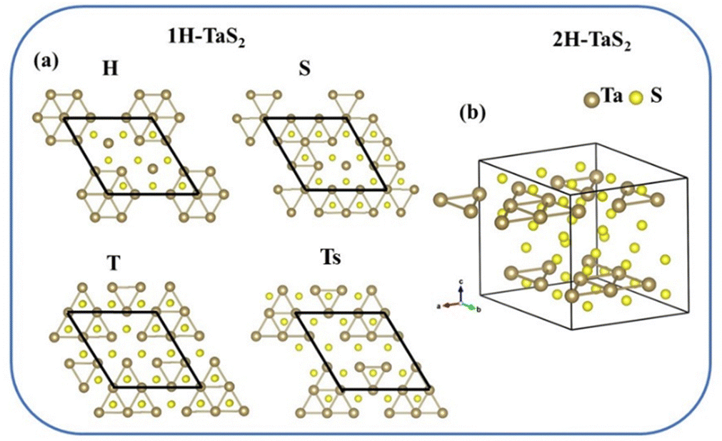 | ||
| Fig. 1 (a) Four types of possible stable images of CDW phase for mono-layer 1H-TaS2. (b) T–Ts configuration of CDW phase for bulk 2H-TaS2. Brown spheres represent tantalum atoms while other spheres represent oxygen atoms. | ||
CDW images (Ta18S36) of bulk 2H-TaS2 were randomly stacked with these four-type images of mono-layer 1H-TaS2. H–T, T–Ts, T–T and Ts–Ts images are actually the same and the most stable structure is shown in Table 1 and Fig. 1(b). This image is very close to the un-distorted T–Ts geometrical structure, therefore the T–Ts image is chosen to represent the geometrical structure of CDW phase for bulk 2H-TaS2. After further calculating the zero vibrational energies of various configurations, we found that these zero vibrational energies have little effect on the formation energies of various isomers at the level of optB86-vdW corrections. Owing to space limitations, the zero vibrational energy correction will no longer be discussed in the subsequent paragraphs.
| Structure | H–S | H–Ts | H–T | S–T | S–Ts | T–Ts | H–H | S–S | T–T | Ts–Ts |
|---|---|---|---|---|---|---|---|---|---|---|
| ΔECDW (meV) | 84.82 | −0.633 | −3.49 | 82.05 | 6.75 | −3.45 | −2.65 | −1.3 | −3.47 | −3.45 |
The T–Ts configuration has the same symmetry in the out-of-plane direction as its metal phase, but each of its two layers has a different geometrical structure from the metal phase. Its symmetry in the in-plane direction breaks during in-plane contracting of Ta atoms. The in-plane area of T–Ts unit cell (Ta18S36) unexpectedly increases by 0.08% and its interlayer spacing of Ta–Ta atoms decreases by 0.08%, finally it has a 0.05% reduction in total volume as shown in Table S1-3 (ESI†). Its thicknesses of both T and Ts sandwich-type structures decrease by 0.004–0.012 Å and the average interlayer separation of S–S atoms in the T–Ts configuration increases by 0.004 Å after shrinkage of Ta atoms. This decrease of thickness of S–Ta–S sandwich-type structure is completely opposite to its increase of thickness in the CDW phase of bulk 1T-TaS2 upon cooling.41 The total energy of CDW configuration can drop by −38 meV/Ta18S36 (−62 meV fall for total energy without vdW and +24 meV enhancement for vdW energy = −38 meV) for only intralayer shrinkage and then its total energy can further drop by −26 meV/Ta18S36 (0 meV change for total energy without vdW and −26 meV fall for vdW energy = −26 meV) for only reduction by 0.08% of interlayer spacing between Ta–Ta atoms if such a hypothetical PT path exists. Higher vdW energy always corresponds to farther average separation of S–S atoms for an OPT-B86b vdW correction, therefore the enhancement for vdW energy (+24 meV) also reveals a larger average interlayer separation of S–S atoms. The stability of the T–Ts configuration is verified through its phonon spectrum and there is no imaginary frequency in the whole BZ as shown in Fig. S1-4 (ESI†), which reveals its dynamical stability.
3.2. Electronic structure of bulk CDW phase
The Fermi surface of the metal phase includes two separate hole-like sheets as shown in Fig. 2(a). In the first BZ as shown in Fig. S1-5 (ESI†), these include two open hole-type cylindrical surfaces along the G–A and K–H lines. The CDW distortion results in six pseudo band gaps (209/130/63 meV at g1/g2/g3 points in the BZ and 112/119/98 meV at g4/g5/g6 points in the BZ) around the saddle points along the G–A and K–H lines. Our theoretical pseudo-gaps at the “g3” and “g6” k-points in the BZ have not been predicted by previous theoretical calculations.14 Since these partially opened pseudo-gaps of CDW phase always appear even in the mono-layer 1H-TaS2 samples as shown in Fig. S1-6 (ESI†), and then the positions of g1–g6 pseudo band gaps are all located at the high symmetry points of the BZ boundary of the CDW phase as shown in Fig. S1-5 (ESI†), the origin of pseudo band gaps for the CDW phase mainly derives from Ta atoms contracting and then electron-lattice coupling plays a key role in driving the formation of CDW for bulk 2H-TaS2. Previous frequency-dependent optical reflectivity measurements42 indicated that the Fermi surface of 2H-TaS2 is only partially gapped in the CDW state. The spectral evolution of two different NaxTaS2 crystals further confirms that the partial-gapped structure observed in 2H-TaS2 clearly corresponds to its CDW transition. The resistivity of 2H-TaS2 remains metallic below TCDW and shows only a small anomaly at the PT, indicating that the CDW does not involve a large modification of the Fermi surface.42,43 Our nesting vector is QFS ≈ 0.86 GM, so it does not satisfy the required nesting condition (QCDW ≈ 0.68 GM) to induce CDW PT. Rice and Scott44 suggested that the two-dimensional conduction band with saddle points close to the Fermi level was unstable against CDW formation. Our CDW vector of the k-space separation between two saddle points is QSP ≈ 0.62 GK, where the Fermi vectors along GK(AH) are in good correspondence with previous band theory44 and experimental observations.45 Our theoretical calculations provided a theoretical support for the “saddle-point” CDW mechanism proposed by Rice and Scott.44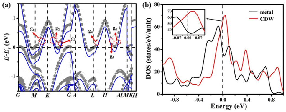 | ||
| Fig. 2 (a) Energy band of metal phase and unfolding energy band of CDW phase for bulk sample. The gray and blue lines represent the CDW and metal phases. The g1–g6 symbols indicate that the pseudo band gaps are located at the g1–g6 points in the BZ, respectively. (b) Total DOS for bulk 2H-TaS2. | ||
Ta atoms in the adjacent two layers do not form chemical bonds owing to being too far away, and can interact only through bridges composed of sulfur atoms. The average distance between sulfur atoms in the adjacent two layers rises from 2.872 Å to 2.876 Å during the PT, which will lead to a weakening of the chemical bonds from their pz orbitals between sulfur atoms in the adjacent two layers. The energy band at the high-symmetry points M–L segment in the out-of-plane direction is mainly composed of a hybrid of the d orbital of Ta atoms and the p orbital of S atoms as shown in Fig. S1-7 (ESI†). The bandwidth is proportional to the overlap integral γ, which decreases exponentially with these S–S atomic separations based on the tight binding theory in solid state physics for energy bands.46 The bandwidth for the energy band at the Fermi level of the CDW phase increases approximately by 20 meV in the in-plane direction owing to contracting of Ta atoms, while it decreases approximately 10 meV in the out-of-plane direction relative to the metal phase owing to farther apart average distance of S–S atoms in the adjacent two layers as shown in Fig. 2(a). Such a decrease of bandwidth in the out-of-plane direction will inevitably lead to an increase in the density of states (DOS) around the Fermi level as shown in Fig. 2(b).
Its total energy of T–Ts configuration drops by 64 meV relative to the supercell of the metal phase with the same number of atoms and then the Fermi surface subsequently drops by 170 meV. The in-plane and out-of-plane whole energy bands upshift by approximately 195 and 243 meV relative to the new Fermi level, respectively. The energy band of the high-symmetry out-of-plane M–L segment finally crosses the Fermi level.
The slope of the total DOS has a reversal at the Fermi level from the metal phase to the CDW phase as shown in Fig. 2(b). This means an emergence of an additional Fermi surface and the pocket vanishing without the change of out-of-plane symmetry, which is called the pocket-vanishing-type Lifshitz transition.
3.3. Electronic structure of mono-layer CDW phase
Binding energy and formation energy are important indicators for describing structural stability. The binding energies of CDW configuration (Ta9S18) of bulk and multi-layer 2H-TaS2 are defined as Eb = (ECDW − 9ETa − 18ES), where ECDW and ETa (or ES) are total energies without vdW correction of the CDW configuration and the cubic unit cell with a 20 Å crystal constant including only one Ta (or S) atom, respectively.Both binding energy and formation energy as shown in Table 2 reveal that the stability of the CDW phase for a mono-layer sample is the poorest in the 2H configurations. Our theoretical PT temperature TCDW from CDW to metal phase is roughly estimated as approximately 59 K for mono-layer 2H-TaS2, which is strongly supported by recent temperature-dependent resistance measurements (TCDW ≈ 50–60 K).14,15
| E b (CDW) | ΔECDW | E vdw (metal) | E vdw (CDW) | D S–S (metal) | D S–S (CDW) | D S–Ta–S (metal) | D S–Ta–S (CDW) | |
|---|---|---|---|---|---|---|---|---|
| T | −138.900 | −0.040 | 30.973 | 30.967 | 3.136 | 3.116 | ||
| Mono-layer | −140.161 | −0.049 | 28.981 | 28.991 | 2.877 | 2.882 | 3.135 | 3.127 |
| Bilayer | −140.736 | −0.053 | 27.963 | 27.965 | 2.876 | 2.881 | 3.137 | 3.128 |
| Trilayer | −140.944 | −0.058 | 27.602 | 27.621 | 2.874 | 2.880 | 3.137 | 3.128 |
| Bulk | −141.399 | −0.062 | 26.919 | 26.919 | 2.872 | 2.876 | 3.138 | 3.130 |
The pseudo band gaps of mono-layer T–Ts configuration are also partially open around the G–A and K–H segments during Ta atoms contracting for mono-layer 2H-TaS2 as shown in Fig. 3(a). The mono-layer CDW phase also has six pseudo band gaps (127/115/56 meV at g1/g2/g3 points in the BZ and 108/118/47 meV at g4/g5/g6 points in the BZ) around the saddle points along the G–A and K–H line in the BZ. The positions of g1–g6 pseudo band gaps are also all located at the high symmetry points of the BZ boundary of the CDW phase. Overall the pseudo band gaps of mono-layer 2H-TaS2 are smaller than corresponding values at all k-points in the bulk samples, which also reveals its poorer stability relative to the bulk samples. Surprisingly, the positions of pseudo band gaps happen to be at the Fermi level for mono-layer Ts configurations in Fig. S1-6 (ESI†) and for mono-layer T–Ts configuration. The projected in-plane DOS will have a significant drop at around the Fermi level when the Fermi surface locates inside the region of pseudo-gaps.
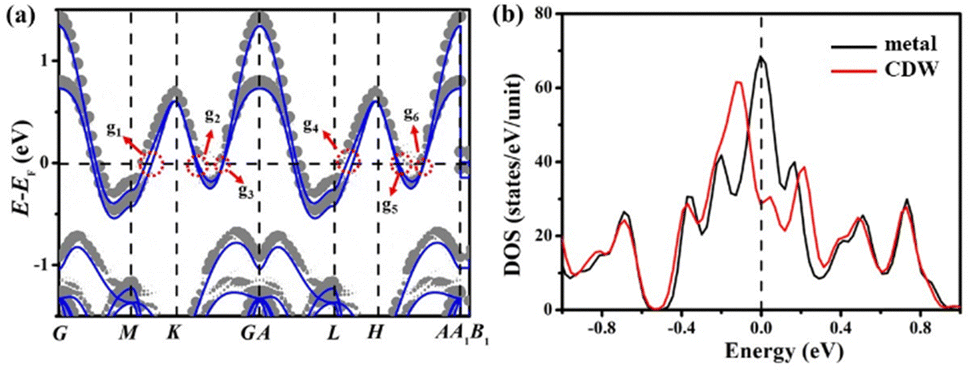 | ||
| Fig. 3 (a) Energy band of metal phase and unfolding energy band of CDW phase for mono-layer sample. The gray and blue lines represent the CDW and metal phases. The g1–g6 symbols indicate that the pseudo band gaps are located at the g1–g6 points in the BZ, respectively. (b) Total DOS for mono-layer 2H-TaS2. | ||
The absolute value of formation energy of a mono-layer sample is smaller than that of a bulk sample, which means that the whole energy band of a mono-layer sample has less enhancement than that of bulk when we put their Fermi surface at the same level. This is why the positions of pseudo band gaps happen to be at the Fermi level for mono-layer Ts configurations and mono-layer T–Ts configuration. Its total energy of T–Ts configuration drops by 49 meV compared with the supercell of the metal phase with the same number of atoms as shown in Fig. 3(a). The Fermi surface also subsequently drops only by 6 meV, while its energy band is shifted upwards only by only 24 meV relative to the new Fermi level. The high-symmetry point M–L segment along the out-of-plane direction does not emerge over the Fermi level, while an additional out-of-plane energy band emerges over the Fermi level and leads to a bulge above the Fermi level as shown in Fig. 3(a and b).
Larger average distance between sulfur atoms in the adjacent two layers and in-plane area of S–Ta–S sandwich-type configurations always corresponds to larger vdW energy for mono-layer samples as shown in Table 2 and Table S1-3 (ESI†). The decrease in binding energy ΔEb = (Eb,bulk − Eb,mono-layer) + (EvdW,bulk − EvdW,mono-layer) = −1.238 − 2.072 = −3.310 (eV) as shown in Table 2. During the stacking from mono-layer to bulk, vdW interaction can contribute more to reducing binding energy, by approximately twice the chemical energy. Moreover, the smaller average distance between sulfur atoms in the adjacent two layers and in-plane area of S–Ta–S sandwich-type configurations in the bulk samples means that its spatial structure is relatively tight or dense. Its structural distortion will release significant formation energy or latent heat during its geometrically structural PT as shown in Table 2. Therefore the Fermi surface has a larger drop in the bulk samples, while it has a smaller drop in the mono-layer samples.
3.4. Temperature dependence of resistivity for 2H-TaS2
The entry of the CDW state below the lock-in temperature 75 K is experimentally detected by a sudden change of the resistivity slope with temperature for bulk 2H-TaS2.11 Its metal phase exhibits a p-type carrier conductivity at room temperature, while the CDW phase exhibits an n-type carrier conductivity below 50 K in the experimental measurements.13 Our theoretical resistivity (description of computational details as shown in Supplementary-II, ESI†) also has a sudden decrease at approximately 75 K from the metal to the CDW phase on cooling as shown in Fig. 5(a). A negative or positive slope of the total DOS at the Fermi level means that n-type or p-type carriers are dominant in the bulk materials. So the dominant p-type carrier conductivity in the metal phase and the n-type carrier conductivity in the bulk CDW phase can be easily found out from their total DOS as shown in Fig. 2(b). Comparing the DOS of the CDW phase with that of the metal phase for bulk samples, it was found that the larger total DOS at the Fermi surface in the CDW phase was mainly attributed to the upshift of in-plane and out-of-plane bands as shown in Fig. S1-8 (ESI†). The opening of the pseudogap reduces the effective number of charge carriers in the pseudogap region, the effective number of charge carriers at several bottoms of electronic pockets i.e. around the middle point of GK(AH) segments significantly rises. This upshift of electronic pockets near the Fermi level is responsible for the larger DOS above the Fermi surface in the in-plane direction as shown in Fig. S1-8(a) and (c) (ESI†). The opening of the pseudogap actually reduces significantly the value of the DOS at the B point as shown in Fig. S1-8(c) and (d) (ESI†), however, it has little influence on the reversal in carrier sign and the slope of the DOS owing to it being far away from the Fermi level for bulk samples.The theoretical resistivity has a sudden decrease at approximately 60 K from the metal to the CDW phase on cooling and tends to flatten out below around 50 K for the CDW phase of mono-layer 2H-TaS2 as shown in Fig. 4(b), which is consistent with recent temperature-dependent-resistivity measurements.14 The out-of-plane DOS still takes a key role in raising the total DOS around the Fermi level as shown in Fig. 3(b) and Fig. S1-9(d) (ESI†). The Fermi surface drops only by 6 meV during PT, and then the B–C segment in Fig. S1-9(c and d) (ESI†) actually locates inside the region of one or two pseudo-gaps as shown in Fig. S1-9(a) (ESI†), which leads to a significant reduction of the in-plane DOS around the Fermi level in Fig. S1-9(c) (ESI†). This causes a reversal of slope for the total DOS in Fig. 3(b) and alternation for p–n type carriers to fail in the mono-layer samples. In this case, only the slope of the projected DOS in the out-of-plane direction has a reversal at the Fermi level during PT, which means that the pocket-vanishing-type Lifshitz transition occurs only in the out-of-plane direction.
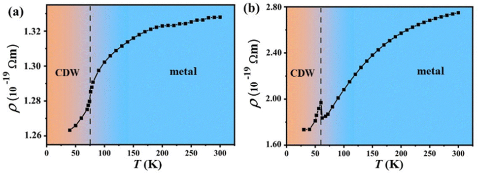 | ||
| Fig. 4 Temperature dependence of theoretical resistivity for 2H-TaS2. (a) Bulk samples, (b) mono-layer samples. | ||
3.5. Doping-induced PT
The formation energies of the bulk 2H-TaS2 (Ta18S36) and mono-layer 2H-TaS2 (Ta18S36) were calculated for the situations of electron and hole doping as shown in Fig. 5. In our calculations of carrier-doping effects, electron (or hole) doping was simulated by increasing (or decreasing) the total number of electrons in the system, together with a compensating uniform positive (or negative) background to maintain charge neutrality. As expected, electron doping always increases the lattice parameters, while hole doping shrinks the lattice. The unit volume of the CDW phase without doping is smaller than that of the metal phase as shown in Table S1-3 (ESI†), so the hole doping will promote the appearance of the CDW phase, while the electron doping suppresses it in the bulk phase as shown in Fig. 5. The smaller magnitude of the change of formation energies for mono-layer samples resulted from its open structure i.e. larger average distance between sulfur atoms in the adjacent two layers as shown in Table 2. Our theoretical PT temperature TCDW from the CDW to the metal phase is roughly estimated as approximately 68 K for mono-layer 2H-TaS2 after hole doping. Recent temperature-dependent resistance experiments16 indicate that mono-layer 2H-TaS2 on SiO2/Si substrates undergoes a PT at 140 K upon heating which is far above that (75 K) of bulk samples. Its higher TCDW was attributed to the reduced dimensionality and enhancement of electron–phonon coupling. However, its larger thermal hysteresis effect (PT temperature at 93 K upon cooling) reveals that its PT is a strong first-order structural PT rather than weak structural T–Ts → metal PT. In fact, after injecting holes, the total energy of some CDW images (called the X image) in Table 1 is significantly reduced. Large geometric structural difference and small energy difference between T–Ts and X configurations can reasonably explain the wider-temperature thermal hysteresis effect16 at low temperature for mono-layer TaS2.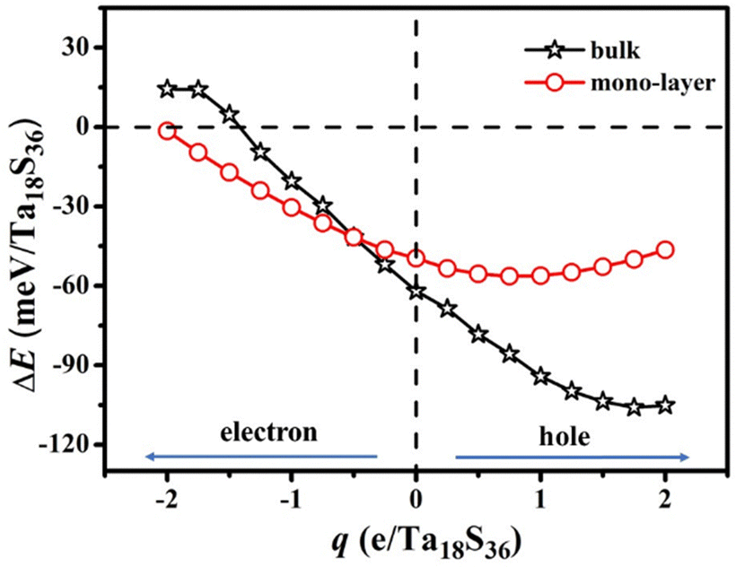 | ||
| Fig. 5 Excess charge dependence of formation energy for bulk and mono-layer materials. | ||
Interestingly, the CDW phase was found to be absent in epitaxial mono-layered 2H-TaS2 on a Au(111) substrate47 but persisted in MBE grown mono-layered TaS2 on graphene/Ir(111).48,49 These findings provided further evidence that the CDW formation in such atomically thin TMDs is, in general, highly susceptible to the surrounding environment that could be a neighboring layer or even a substrate. One important difference between these two substrates is that Au(111) as a metal is a better electron dopant than graphene that is a semimetal. We calculated the 2H-TaS2 mono-layer/Au(111) and 2H-TaS2 mono-layer/graphene systems and then performed Bader charge analysis to study the electron transfer from the substrate to 2H-TaS2. It is found that TaS2 (Ta18S36) obtains 0.71e from Au(111), which is sufficient to suppress the 3 × 3 CDW phase according to electron doping to induce the CDW phase. Recent theoretical calculations50 indicated that there is a charge transfer of about 1.44e from Au(111) to each 2H-TaS2 mono-layer. Such a quantity of charge injection can more effectively suppress the occurrence of the CDW phase. Since the CDW phase of the mono-layer model is more reasonable as mentioned above, our theoretical results are more reliable owing to the mono-layer 2H-TaS2 model used in their calculations. The electron doping level from mono-layered and bilayered graphene to 2H-TaS2 significantly reduces to 0.39e and 0.37e, respectively, which is low enough to keep the 3 × 3 CDW phase. Although the substrate effects are complex and usually cannot be ascribed to one single factor, the difference of the electron doping contributed by Au(111) and graphene is already large enough to affect the CDW phase in 2H-TaS2, leading to different experimental observations.47–49
3. Conclusions
The geometrical structure (T–Ts) of the CDW phase with several pseudo-gaps (50–200 meV order of magnitude) was predicted through first principles calculations for bulk and mono-layer 2H-TaS2. Driven by electron-lattice coupling, Ta atoms contract to form the CDW phase and the Fermi level continually drops on cooling. Its whole energy bands upshift and then the positions of the pseudo band gap finally become much higher (around 200 meV) relative to the Fermi level for the bulk sample, while they happen to be at the Fermi level for mono-layer samples. The vdW interaction makes bulk samples have larger density and latent heat, which result in a larger upshift for the whole energy bands in the bulk samples.The average interlayer separation of S–S atoms in the adjacent two layers increases after the shrinkage of Ta atoms for bulk samples during PT, which leads to a weaker chemical bonding among S–S atoms in the adjacent two layers. Its bandwidth in the out-of-plane direction of the CDW phase decreases relative to the metal phase owing to the weaker chemical bonding, which results in a substantial bulge of the projected out-of-plane DOS and total DOS around the Fermi level. However, the existence of the pseudo band gap will reduce the projected in-plane DOS and then total DOS around the Fermi level for mono-layer samples. The bulge for the total DOS of the CDW phase located at the Fermi level is responsible for the n-type carrier in the bulk 2H-TaS2, while the reduction of the total DOS owing to the existence of the pseudo-gap at the Fermi level is responsible for the p-type carrier in the mono-layer 2H-TaS2.
The T–Ts configuration has the same symmetry in the out-of-plane direction as its metal phase, but each of its two layers has a different geometrical structure from the metal phase. Its symmetry in the in-plane direction breaks during in-plane contracting of Ta atoms. Lifshitz transition with an emergence of additional Fermi surface occurs in the out-of-plane direction without symmetry breaking during the structural PT. Our CDW vector of the k-space separation between two saddle points is QSP ≈ 0.62 GK and can provide a theoretical support for the “saddle-point” CDW mechanism proposed by Rice and Scott.
Conflicts of interest
There are no conflicts to declare.Acknowledgements
This work was supported by the National Natural Science Foundation of China under Grants (No. 51872227, 51572219).References
- I. M. Lifshitz, Anomalies of electron characteristics of a metal in the high pressure region, J. Exp. Theor. Phys., 1960, 11, 1130–1135 Search PubMed.
- A. Fang, T. Koschny and C. M. Soukoulis, Self-consistent calculations of loss-compensated fishnet metamaterials, Phys. Rev. B: Condens. Matter Mater. Phys., 2010, 82, 121102 CrossRef.
- R. Guo, Z. A. Zhu, Y. B. Chen, S. H. Yao and J. Zhou, First-principles calculations of structural and electronic properties of layered AxRhO2 (A = Li, Na, K, Rb, Cs), AIP Adv., 2020, 10, 035320 CrossRef CAS.
- C. Van Efferen, J. Berges, J. Hall, E. Loon, S. Kraus, A. Schobert, T. Wekking, F. Huttmann, E. Plaar, N. Rothenbach, K. Ollefs, L. M. Arruda, N. Brookes, G. Schönhoff, K. Kummer, H. Wende, T. Wehling and T. Michely, A full gap above the Fermi level: the charge density wave of monolayer VS2, Nat. Commun., 2021, 12, 6837 CrossRef CAS PubMed.
- Y. Lemonik, I. L. Aleiner, C. Toke and V. I. Falko, Spontaneous symmetry breaking and Lifshitz transition in bilayer graphene, Phys. Rev. B: Condens. Matter Mater. Phys., 2010, 82, 201408 CrossRef.
- M. H. Van Maaren and H. B. Harland, An energy band model of Nb-and Ta-dichalcogenide superconductors, Phys. Lett. A, 1969, 29, 571–573 CrossRef CAS.
- A. H. Thompson, F. R. Gamble and R. F. Koehler, Effects of intercalation on electron transport in tantalum disulfide, Phys. Rev. B: Solid State, 1972, 5, 2811 CrossRef.
- J. P. Tidman, O. Singh, A. E. Curzon and R. F. Frindt, The phase transition in 2H-TaS2 at 75 K, Philos. Mag., 1974, 30, 1191–1194 CrossRef CAS.
- J. A. Wilson, F. J. Di Salvo and S. Mahajan, Charge-density waves and superlattices in the metallic layered transition metal dichalcogenides, Adv. Phys., 1975, 24, 117–201 CrossRef CAS.
- J. P. A. A. Chevalier and W. M. Stobbs, Electron diffraction effects in 2H-TaS2, Philos. Mag., 1975, 31, 733–737 CrossRef CAS.
- S. J. Hillenius and R. V. Coleman, Quantum oscillations and the Fermi surface of 2H-TaS2, Phys. Rev. B: Condens. Matter Mater. Phys., 1978, 18, 3790 CrossRef CAS.
- M. Naito and S. Tanaka, Electrical transport properties in 2H-NbS2,-NbSe2,-TaS2 and -TaSe2, J. Phys. Soc. Japan, 1982, 51, 219–227 CrossRef CAS.
- K. Zhang, Z. Y. Cao and X. J. Chen, Effects of charge-density-wave phase transition on electrical transport and Raman spectra in 2H-tantalum disulfide, Appl. Phys. Lett., 2019, 114, 141901 CrossRef.
- Y. Yang, S. Fang, V. Fatemi, J. Ruhman, E. Navarro-Moratalla, K. Watanabe, T. Takashi, E. Kaxiras and P. Jarillo-Herrero, Enhanced superconductivity upon weakening of charge density wave transport in 2H-TaS2 in the two-dimensional limit, Phys. Rev. B, 2018, 98, 035203 CrossRef CAS.
- D. Lin, S. Li, J. Wen, H. Berger, L. Forro, H. B. Zhou, S. Jia, T. Taniguchi, K. Watanabe, X. X. Xi and M. S. Bahramy, Patterns and driving forces of dimensionality-dependent charge density waves in 2H-type transition metal dichalcogenides, Nat. Commun., 2020, 11, 2406 CrossRef CAS PubMed.
- W. Liu, Z. Duan, C. Zhang, X. X. Hu, J. B. Cao, L. J. Liu and L. Liu, Experimental observations and density functional simulations on the structural transition behavior of a two-dimensional transition-metal dichalcogenide, Sci. Rep., 2020, 10, 18255 CrossRef CAS PubMed.
- R. W. Cohen, G. D. Cody and J. J. Halloran, Effect of Fermi-level motion on normal-state properties of β-tungsten superconductors, Phys. Rev. Lett., 1967, 19, 840 CrossRef CAS.
- J. B. Goodenough, Band model for transition–metal Chalcogenides having layer structures with occupied trigonal-bipyramidal sites, Mat. Res. Bull., 1968, 3, 409 CrossRef CAS.
- R. A. Bromley, A Fermi Surface for 2H-NbSe2, Phys. Rev. Lett., 1972, 29, 357 CrossRef CAS.
- D. V. Evtushinsky, A. A. Kordyuk, V. B. Zabolotnyy, D. S. Inosov, B. Buchner, H. Berger, L. Patthey, R. Follath and S. V. Borisenko, Pseudogap-driven sign reversal of the Hall effect, Phys. Rev. Lett., 2008, 100, 236402 CrossRef CAS PubMed.
- H. W. Du, Z. Y. Jiang, J. M. Zheng, X. D. Zhang, W. X. Wang and Z. Y. Zhang, Theoretical study of CDW phases for bulk NbX2 (X= S and Se), Phys. Chem. Chem. Phys., 2024, 26(3), 2376–2386 RSC.
- H. N. S. Lee, M. Garcia, H. McKinzie and A. Wold, The low-temperature electrical and magnetic properties of TaSe2 and NbSe2, J. Solid State Chem., 1970, 1, 190–194 CrossRef CAS.
- A. H. Thompson, R. F. Gamble and J. F. Revelli, Transitions between semiconducting and metallic phases in 1T-TaS2, Solid State Commun., 1971, 9, 981–985 CrossRef CAS.
- X. Xi, L. Zhao, Z. Wang, H. Berger, L. Forro, J. Shan and K. F. Mak, Strongly enhanced charge-density-wave order in monolayer NbSe2, Nat. Nanotechnol., 2015, 10, 765–769 CrossRef CAS PubMed.
- R. Bianco, L. Monacelli, M. Calandra, F. Mauri and I. Errea, Weak dimensionality dependence and dominant role of ionic fluctuations in the charge-density-wave transition of NbSe2, Phys. Rev. Lett., 2020, 125, 106101 CrossRef CAS PubMed.
- C. Boix-Constant, S. Mañas-Valero, R. Córdoba, J. J. Baldivi, A. Rubio and E. Coronado, Out-of-plane transport of 1T-TaS2/graphene-based van der Waals heterostructures, ACS Nano, 2021, 15, 11898–11907 CrossRef CAS PubMed.
- G. Kresse and J. Furthmüller, Efficient iterative schemes for ab initio total-energy calculations using a plane-wave basis set, Phys. Rev. B: Condens. Matter Mater. Phys., 1996, 54, 11169–11186 CrossRef CAS PubMed.
- G. Kresse and D. Joubert, From ultrasoft pseudopotentials to the projector augmented-wave method, Phys. Rev. B: Condens. Matter Mater. Phys., 1999, 59, 1758 CrossRef CAS.
- J. Klimes, D. R. Bowler and A. Michaelides, Chemical accuracy for the van der Waals density functiona, J. Phys.: Condens. Matter, 2019, 22, 022201 CrossRef PubMed.
- Y. W. Li, J. Jiang, H. F. Yang, D. Prabhakaran, Z. K. Liu, L. X. Yang and Y. L. Chen, Folded superstructure and degeneracy-enhanced band gap in the weak-coupling charge density wave system 2H-TaSe2, Phys. Rev. B, 2018, 97, 115118 CrossRef CAS.
- L. Chaput, A. Togo, I. Tanaka and G. Hug, Phonon-phonon interactions in transition metals, Phys. Rev. B: Condens. Matter Mater. Phys., 2011, 84, 094302 CrossRef.
- Y. Wang, L. Yan and Y. Ma, Lattice Boltzmann solution of the transient Boltzmann transport equation in radiative and neutron transport, Phys. Rev. E, 2017, 95, 063313 CrossRef PubMed.
- V. Wang, N. Xu, J. C. Liu, G. Tang and W. T. Geng, VASPKIT: A user-friendly interface facilitating high-throughput computing and analysis using VASP code, Comput. Phys. Commun., 2021, 267, 108033 CrossRef CAS.
- S. L. Dudarev, G. A. Botton, S. Y. Savrasov, C. J. Humphreys and A. P. Sutton, Electron-energy-loss spectra and the structural stability of nickel oxide: An LSDA + U study, Phys. Rev. B: Condens. Matter Mater. Phys., 1998, 57, 1505 CrossRef CAS.
- T. Jiang, T. Hu, G. D. Zhao, Y. C. Li, S. W. Xu, C. Liu, Y. N. Cui and W. Ren, Two-dimensional charge density waves in TaX2 (X = S, Se, Te) from first principles, Phys. Rev. B, 2021, 104, 075147 CrossRef CAS.
- S. Sharma, S. Auluck and M. A. Khan, Optical properties of 1T and 2H phase of TaS2 and TaSe2, Pramana, 2000, 54, 431–440 CrossRef CAS.
- Y. Zheng, X. Jiang, X. X. Xue, X. L. Yao, J. Zeng, K. Q. Chen, E. Wang and Y. Feng, Nuclear Quantum Effects on the Charge-Density Wave Transition in NbX2 (X= S, Se), Nano Lett., 2022, 22, 1858–1865 CrossRef CAS PubMed.
- B. Guster, C. Rubio-Verdú, R. Robles, J. Zaldívar, P. Dreher, M. Pruneda, J. A. Silva-Guillen, D. J. Choi, J. I. Pascual, M. M. Ugeda, P. Ordejon and E. Canadell, Coexistence of Elastic Modulations in the Charge Density Wave State of 2H-NbSe, Nano lett., 2019, 19, 3027–3032 CrossRef CAS PubMed.
- C. S. Lian, C. Si and W. Duan, Unveiling charge-density wave, superconductivity, and their competitive nature in two-dimensional NbSe2, Nano Lett., 2018, 18, 2924–2929 CrossRef CAS PubMed.
- R. Bianco, I. Errea, L. Monacelli, M. Calandra and F. Mauri, Quantum enhancement of charge density wave in NbS2 in the two-dimensional limit, Nano Lett., 2019, 19, 3098–3103 CrossRef CAS PubMed.
- X. L. Yu, D. Y. Liu, Y. M. Quan, J. S. Wu, H. Q. Lin, K. Chang and L. J. Zou, Electronic correlation effects and orbital density wave in the layered compound 1T-TaS2, Phys. Rev. B, 2017, 96, 1138 Search PubMed.
- W. Z. Hu, G. Li, J. Yan, H. H. Wen, G. Wu, X. H. Chen and N. L. Wang, Optical study of the charge-density-wave mechanism in 2H−TaS2 and NaxTaS2, Phys. Rev. B: Condens. Matter Mater. Phys., 2007, 76, 045103 CrossRef.
- J. M. E. Harper, T. H. Geballe and F. J. Di Salvo, Heat capacity of 2H-NbSe2 at the charge density wave transition, Phys. Lett. A, 1975, 54, 27–28 CrossRef.
- T. M. Rice and G. K. Scott, New mechanism for a charge-density-wave instability, Phys. Rev. Lett., 1975, 35, 120 CrossRef CAS.
- R. Liu, C. G. Olson, W. C. Tonjes and R. F. Frindt, Momentum Dependent Spectral Changes Induced by the Charge Density Wave in 2H-TaSe2 and the Implication on the CDW Mechanism, Phys. Rev. Lett., 1998, 80, 80 Search PubMed.
- C. Kittel and P. McEuen, Introduction to solid state physics, Wiley, New York, 2005, p. 235 Search PubMed.
- C. E. Sanders, M. Dendzik, A. S. Ngankeu, A. Eich, A. Bruix, M. Bianchi, J. A. Miwa, B. Hammer, A. A. Khajetoorians and P. Hofmann, Crystalline and electronic structure of single-layer TaS2, Phys. Rev. B, 2016, 94, 081404 CrossRef.
- J. Hall, N. Ehlen, J. Berges, E. V. Loon, C. V. Efferen, C. Murray, M. Rosner, J. Li, B. V. Senkovskiy, M. Hell, M. Rolf, T. Heider, M. C. Asensio, J. Avila, L. Plucinski, T. Wehling, A. Grüneis and T. Michely, Environmental control of charge density wave order in monolayer 2H-TaS2, ACS Nano, 2019, 13, 10210–10220 CrossRef CAS PubMed.
- D. Lin, S. Li, J. Wen, H. Berger, L. Forro, H. Zhou, S. Jia, T. Taniguchi, K. Watanabe, X. X. Xi and M. S. Bahramy, Patterns and driving forces of dimensionality-dependent charge density waves in 2H-type transition metal dichalcogenides, Nat. Commun., 2020, 11, 2406 CrossRef CAS PubMed.
- C. C. Silva, D. Dombrowski, A. Samad, J. Q. Cai, W. Jolie, J. Hall, P. T. P. Ryan, P. K. Thakur, D. A. Duncan, T. L. Lee, U. Schwingenschlog and C. Busse, Structure of monolayer 2H-TaS2 on Au (111), Phys. Rev. B, 2021, 104, 205414 CrossRef CAS.
Footnote |
| † Electronic supplementary information (ESI) available. See DOI: https://doi.org/10.1039/d4cp00977k |
| This journal is © the Owner Societies 2024 |