
 Open Access Article
 This Open Access Article is licensed under a Creative Commons Attribution-Non Commercial 3.0 Unported Licence
Atomic force microscopy observation of surface morphologies and measurements of local contact potential differences of amorphous solid water samples deposited at 15 and 100 K†
Takuto
Tomaru
 ,
Hiroshi
Hidaka
*,
Akira
Kouchi
and
Naoki
Watanabe
,
Hiroshi
Hidaka
*,
Akira
Kouchi
and
Naoki
Watanabe
Institute of Low Temperature Science, Hokkaido University, N19W8, Kita-ku, Sapporo 0600819, Japan. E-mail: hidaka@lowtem.hokudai.ac.jp
First published on 30th April 2024
Abstract
We use an ultra-high vacuum cryogenic atomic force microscope to investigate the surface morphology of amorphous solid water (ASW) prepared by oblique deposition of water vapor onto Si(111)7 × 7 substrates at temperatures of 15 and 100 K. Height–height correlation function analysis of topographic images suggests that ASW at 15 K has a columnar structure and that the typical diameter of the column is 5–10 nm. At 100 K, the typical diameter is 10–30 nm, although columnar features are less prominent. The surface roughness (i.e., deviation of the height) is greater at 15 K than at 100 K, indicating that the surface at 100 K exhibits a relatively flat morphology. This result implies that transient diffusion of deposited water molecules affects the surface morphology at 100 K. In addition, measurements of the local contact potential difference between the tip and the ASW surface suggest that the magnitude of the negative surface potential at the microscopic scale, which is attributed to spontaneous polarisation, cannot simply be scaled by the thickness of ASW as predicted in previous experiments with Kelvin probes.
Introduction
Icy dust grains, which are mineral nanoparticles covered with an amorphous ice mantle primarily composed of H2O, have been found in interstellar molecular clouds. These icy dust particles play a critical role in chemical evolution in space because the icy dust surface facilitates various molecular syntheses through processes such as adsorption, diffusion, reaction and desorption of atoms and molecules.1,2 In addition, the icy grains play an important role in mass evolution by the formation of planetesimals3,4 through the collisional growth between icy dust particles. These amorphous-ice-related phenomena have been studied experimentally using vapor-deposited amorphous ice (i.e. amorphous solid water (ASW)) as a mimic of an amorphous ice mantle because it is difficult to prepare a more realistic amorphous ice mantle, which should be formed by chemical reactions of oxygen and hydrogen on a silicate surface.5,6 To accurately evaluate the experimental results for these phenomena, knowledge of the morphology of vapor-deposited ASW becomes critical. Therefore, many studies on the morphology of vapor-deposited ASW have been conducted both theoretically and experimentally.Numerical simulations using a ballistic model with hard spheres have been widely used to investigate thin-film structures obtained through molecular beam deposition.7–9 However, the morphology of amorphous thin films obtained from these models might not be realistic because the physicochemical properties of water molecules and ice were not taken into account in the associated studies. Recently, more sophisticated simulations of ASW have been conducted using kinetic Monte Carlo10 and molecular dynamics calculations.11 Clements et al.12 used a kinetic Monte Carlo model to examine how the ASW morphology is affected by various deposition parameters such as the deposition temperature, rate of deposition and deposition angle to the substrate. They treated the surface diffusion kinetics with the rate of hopping between surface adsorption sites. They claimed their model was valid because it reproduced the temperature dependence of ASW densities obtained in experiments.13 However, because the density does not necessarily have a one-to-one correspondence with the morphology, whether the simulated morphology truly reflects the characteristics of actual ASW remains unclear. Thus, to refine simulation models more realistically, comparisons with experimentally obtained morphological data are critical.
Previous experimental studies on ASW have been focused mainly on physical properties such as density13–16 and surface area.17–20 Stevenson et al.19 demonstrated that the surface area of ASW varies dramatically with the deposition angle and the substrate temperature. Their results indicate that the formation conditions strongly influence the morphology of ASW.
Scanning probe microscopy (SPM) is one of the valid methods for imaging surface morphology, and it has been applied to ASW in a few instances. Because ASW has very low electrical conductivity, scanning tunnelling microscopy (STM) observations have been limited to very thin ASW samples of 1–2 molecular layers.21,22 Although STM observations of few-nanometre-thick ASW have been attempted,23 a high bias voltage was required, raising concerns about the influence of the electric field on the observed morphology. By contrast, atomic force microscopy (AFM) is more suitable than STM for observing the surface morphology of thick ASW because it does not require samples to be electrically conductive. Nevertheless, the only reported AFM study on thick ASW films is that of Donev et al.,24 who investigated 14 nm-thick ASW films formed on an Au(111) substrate at temperatures ranging from 80 to 108 K. However, the surface morphology of the ASW films was not clearly observed because of the low resolution of the observations. In addition, the ASW samples in their study were prepared at temperatures greater than 80 K. No observations of ASW deposited at lower temperatures comparable to interstellar conditions have been reported. A systematic study of ASW deposited at low and high temperatures is highly desirable.
In addition to the morphology of ASW, the local electric field on the surface of interstellar icy dust plays a role in physicochemical processes that occur on the ASW surface. For example, the ortho-to-para conversion of hydrogen molecules on ice25 might originate from the strong electric field on ice, and the ortho-to-para ratio of the hydrogen molecules strongly affects chemical evolution in space.26 ASW deposited below 130 K is known to be spontaneously polarised, showing a negative potential at the vacuum–ice interface with respect to the substrate. This polarisation phenomenon has been observed not only in ASW thin films but also in several molecular thin films formed at low temperatures using molecules that have a permanent dipole moment.27 The phenomenon in ASW thin films has mainly been studied using the Kelvin probe method28,29 and is known to depend on the formation conditions such as thickness, deposition angle and substrate temperature. These previously reported results suggest that the polarisation phenomenon of ASW thin films might be correlated with the morphology of ASW. That is, the negative surface potential is expected to differ at the nanoscale at each site on the surface irregularities. However, in previous related studies, the negative surface potential was obtained as an average over the entire ASW surface because Kelvin probe measurements lack high spatial resolution. Thus, the nanoscale distribution of the local surface potential on ASW remains unclear. Considering the local surface potential distribution in conjunction with the surface topographic data will contribute to exploring the polarisation mechanisms of ASW thin films.
In the present study, we used ultra-high vacuum low-temperature AFM to visualise the surface morphology and the local surface potential distribution depending on the formation conditions of ASW. The deposition temperature was selected as the key parameter for the formation conditions, and the experiments were conducted at two temperatures, 15 and 100 K, at which significant changes in the morphology are expected.
Experimental
Experimental setup
This study employed an ultra-high vacuum low-temperature STM/AFM system (Infinity, Scienta Omicron). The preparation and observations of ASW samples were both conducted in the ultra-high vacuum chamber. The base pressure was typically ∼10−9 Pa. This apparatus used a liquid helium-free cooling system with a pulse tube cryocooler (RP-062BS, Sumitomo Heavy Industries) to maintain the scanning probe microscope head at ∼10 K for an extended period.The pulse tube cryocooler is a type of helium refrigerator designed without any moving parts inside the cold head. This design, aimed at minimizing vibrational noise, allows the usage of helium refrigerators in SPM systems. A custom-made gas introduction system consisting of a water-vapor reservoir, a variable leak valve (ZLVM-940R, VG), a microcapillary plate (J5022-01, Hamamatsu) and an XYZ stage for collimating water vapor was added.
Although a tungsten probe was attached to the standard qPlus sensor, which is the force sensor using a tuning fork-type quartz crystal developed by Giessibl,30 in this system, a qPlus sensor with a sharper tip was made by gluing the tip part of a commercially available cantilever to carry out high-resolution observations of the surface morphology of ASW. Two types of cantilevers were used depending on the purpose of the observations. For the surface topography observations of ASW, a carbon tip (MSS-FM2, nanotools) with a curvature radius of ∼1 nm was used. For measurements of the local contact potential difference, a PtSi tip (PtSi-NCH, Nanosensors) with a radius of curvature of <25 nm was used because of the requirement of electrical conductivity. To ensure sufficient conductivity between the tip and the electrode printed on a quartz tuning fork for monitoring the tunnelling current, the tip and the electrode were connected to each other using silver epoxy (EPO-TEK H20E, Epoxy Technology). The typical resonance frequency, spring constant and Q-factor values for the custom-made qPlus sensor were 26.5 kHz, 1800 N m−1 and 1 × 10⁵, respectively. All AFM observations were conducted using a frequency-modulation mode with a constant oscillation amplitude.
Preparation of ASW samples
We used a Si(111)7 × 7 substrate prepared by heating it at ∼1200 °C under vacuum conditions of less than 9 × 10⁻⁸ Pa. The formation of a clean 7 × 7 structure by surface reconstruction was confirmed by STM with atomic resolution. Water was purified under vacuum via freeze–thaw cycles. ASW samples were produced on the cold Si(111)7 × 7 surface by oblique deposition of water vapor through a microcapillary plate with an incident angle of 60° to the substrate (Fig. 1).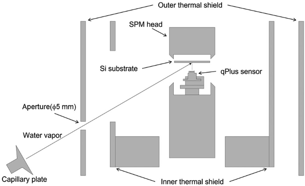 | ||
| Fig. 1 Schematic of the inside of the observation chamber. The SPM head is surrounded by the inner 10 K and the outer 100 K thermal shields. Water vapor at room temperature is deposited after passing through a 5 mm-diameter aperture on the outer shield with an incident angle of 60° to the substrate. | ||
During deposition, the qPlus sensor was fully retracted to exclude the effect of the qPlus sensor on the morphology of the ASW sample. A ceramic heater and a silicon diode sensor (DT-670-SD, Lake Shore) placed near the substrate enabled us to control the substrate temperature. In the present study, the deposition temperature was set to 15 or 100 K, and the duration of the deposition was 30 min. However, for the deposition at 15 K, the substrate temperature gradually increased and reached 23 K within the initial 15 min because of the radiation from the room temperature through a 5-mm aperture on the outer thermal shield. After the vapor deposition, the aperture was immediately closed, resulting in rapid cooling of the substrate to 15 K. We did not observe any temperature change during the deposition at 100 K.
The thickness of the ASW samples was measured using the following method: (1) the ASW samples were deposited onto the 15-K Si(111)7 × 7 surface for a duration between 5 and 10 min; (2) a part of the ASW sample was sputtered by a strong tunnelling current using STM to form a square hole to provide access to the Si substrate (Fig. 2a); (3) by measuring the hole depth using AFM, we obtained the relationship between the duration of the deposition and the depth of the hole (i.e., the ASW thickness) (Fig. 2b). We found that the thickness of ASW produced by deposition for 30 min at a rate of 0.5 nm min−1 was approximately 13.5 nm.
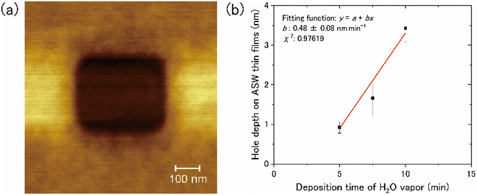 | ||
| Fig. 2 (a) AFM image of a square hole made by strong tunnelling current using a scanning tunnelling microscope. (b) The relationship between hole depth and deposition time at 15 K. The red line represents the result of data fitting using a linear function. | ||
Measurement of the local contact potential difference
The force working at distance r between the tip and the sample surface is composed of several factors, as described by the following equation:| F(r) = Frep(r) + Fchem(r) + FvdW(r) + Fel(r) | (1) |
 | (2) |
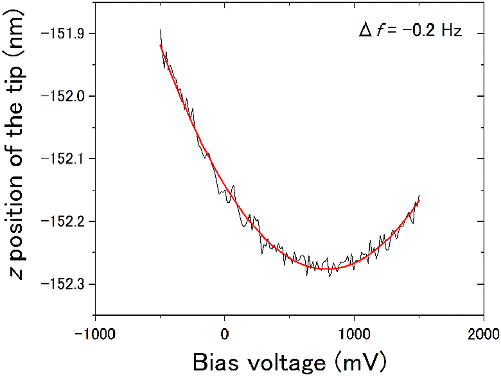 | ||
| Fig. 3 V Bias dependence of z-positions of the tip at a single measurement point on ASW at 15 K while maintaining a constant frequency shift of Δf = −0.2 Hz. Lower z values indicate that the tip positions are closer to the ASW surface. The fitting function (red curve) was a quadratic function. The bias voltage at the vertex of the quadric function indicates a negative VLCPD at the measurement point. | ||
Results and discussion
Temperature dependence of the surface morphology of ASW
Typical topographic images of the ASW sample surface formed at 15 and 100 K are presented two-dimensionally in Fig. 4(a) and (b), respectively, and three-dimensionally in Fig. 4(c) and (d), respectively. The images cover an area of 300 nm × 300 nm. The arrows in the figures indicate the direction of water-vapor incidence. The surface morphologies at the respective temperatures differ substantially, revealing that the surface morphology at 15 K is finer and sharper than that at 100 K. From the height profiles in Fig. 4(e) and (f), the typical lateral scales of surface irregularities at 15 and 100 K are approximately 5–10 and 10–30 nm, respectively. STM topographic surface morphology images have been previously reported for 6 nm-thick ASW on Pt(111) at 100 K,23 and noncontact AFM (NC-AFM) surface morphology images have been reported for 14 nm-thick ASW on Au(111) at 108 K.24 The estimated lateral scale of surface irregularities in 6 and 14 nm-thick ASW samples is 5–10 and 25–40 nm, respectively. The latter scale observed using NC-AFM is similar to the result obtained in the present work, likely because of the similarities in the experimental conditions (e.g., thickness and vapor deposition method) used in the studies. However, the scale observed using STM is measurably smaller than the present result, which might be attributable to the difference in its thickness. Unfortunately, because details of the sample preparation method were not reported in the previous STM study, the differences between the present and the previously reported results are difficult to explain. No previous studies have reported visualisation of the surface morphology of ASW below 100 K. Therefore, a comparison of the topographic images obtained in the present study at these two temperatures holds significant value.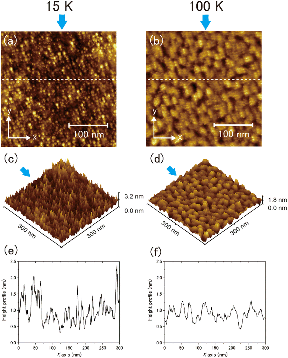 | ||
| Fig. 4 Top panels show the topographic images of an ASW surface observed at (a) 15 K with Δf = −0.26 Hz and VBias = −3000 mV and (b) 100 K with Δf = −0.22 Hz and VBias = −3000 mV using a tip with a curvature radius of ∼1 nm. Middle panels show the 3D representations of surface topographies at (c) 15 K and (d) 100 K. These figures are shown in the same scale height. The bottom panels show the height profiles at (e) 15 K and (f) 100 K, and the places are indicated by white dashed lines in (a) and (b), respectively. Arrows indicate the deposition direction of water vapor. | ||
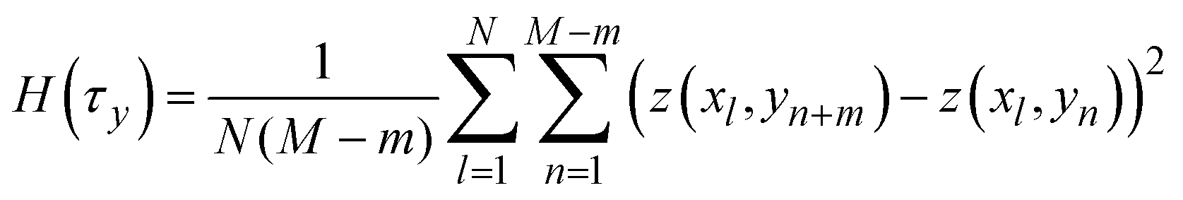
To further evaluate the difference between the surface morphology at 15 and 100 K quantitatively, we performed data analysis using the height–height correlation function (HHCF)32,33 defined as the mean square of height difference between two measurement points separated by the displacement vector ![[small tau, Greek, vector]](https://www.rsc.org/images/entities/i_char_e1ca.gif) as follows:
as follows:
H() = 〈[z(![[r with combining right harpoon above (vector)]](https://www.rsc.org/images/entities/i_char_0072_20d1.gif) ) − z( − )]2〉 ) − z( − )]2〉 | (3) |
indicates a position vector of any specific measurement point. We applied this HHCF analysis to the x and y directions in the AFM image, separately. Thus, H(τx) and H(τy) were calculated using the following equation: | (4) |
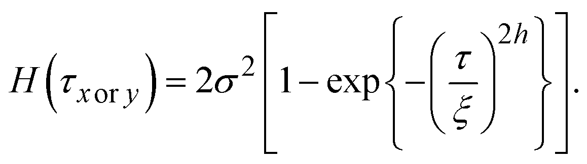
 | (5) |
 | (6) |
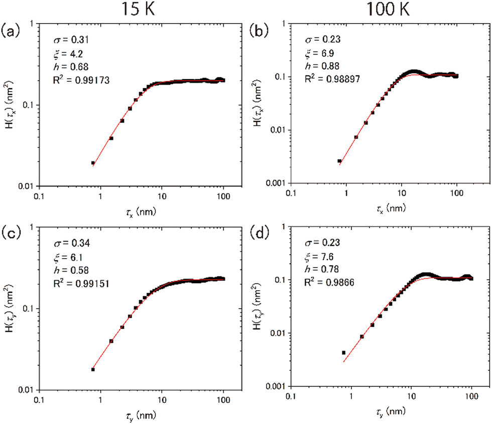 | ||
| Fig. 5 Plots of HHCF analysis with fitting results using topographic data at (a) and (c) 15 K and (b) and (d) 100 K. (a) and (b) The results for x-direction analysis and (c) and (d) those for y-direction analysis. | ||
However, the values are almost equivalent irrespective of the direction at 100 K: 6.9 and 7.6 nm for the x and y directions, respectively. Table 1 summarises the results of the HHCF analysis for several topographic data. These averaged values also indicate that the analytical direction dependence appeared only in the ξ value at 15 K, which means that this dependence is not specific to the data shown in Fig. 4 but is instead specific to the general characteristics associated with the sample preparation method.
| x-direction analysis | y-direction analysis | |||
|---|---|---|---|---|
| 15 K | 100 K | 15 K | 100 K | |
| σ (nm) | 0.32 ± 0.04 | 0.24 ± 0.03 | 0.33 ± 0.05 | 0.24 ± 0.03 |
| ξ (nm) | 4.3 ± 0.5 | 7.4 ± 0.3 | 7.0 ± 0.9 | 7.7 ± 0.3 |
| h | 0.67 ± 0.04 | 0.89 ± 0.01 | 0.58 ± 0.01 | 0.82 ± 0.02 |
Numerous studies on the morphology of thin films of several materials (e.g., metals, semiconductors, metal oxides and fluorides) produced by sputtering or vapor deposition have been reported.37–39 A morphology classification system based on the relationship between the deposition temperature T and the melting point Tm has been established. For instance, in the region where T/Tm < 0.1, the morphology is predominantly influenced by shadowing effects, resulting in a characteristic structure referred to as a columnar structure. A simple model has been proposed to determine the growth angle of columns at a given incident angle of the molecular beam.40 In the region where 0.1 < T/Tm < 0.3, surface diffusion of the deposited molecules is believed to govern the morphology, whereas bulk diffusion is predominant in the region where 0.3 < T/Tm < 1. However, the growth angle exhibits material dependence even when the deposition angle remains constant in the formation of thin metal films.41 Whether the classification of film structures using the T/Tm function is applicable to ASW has not yet been determined.
For the water vapor deposition at 15 K (T/Tm = 0.06), the ASW sample is expected to have a columnar structure tilted in the direction of water vapor deposition. Fig. 6 presents schematics of the columnar structure observed from two different angles relative to the direction of vapor deposition. Because of the tilting of the columnar structure, the lateral size of surface irregularities parallel to the water vapor direction would be larger than those perpendicular to the water vapor direction. Under these conditions, the correlation lengths obtained through HHCF analysis are expected to differ between the two directions. Thus, the direction-dependent HHCF analysis results at 15 K suggest the presence of a columnar structure in the ASW sample. In the 100 K ASW sample, the structure is expected to be determined by surface diffusion and/or bulk diffusion because T/Tm = 0.37. The observed difference in correlation lengths ξ at 100 K was minimal, which is reasonable because the structure of the ASW sample determined by surface and/or bulk diffusion at 100 K should not exhibit a deposition direction dependence. The consistency between the structure classified using T/Tm and the direction dependence of HHCF analysis on the correlation length demonstrates that the structure of the whole film can be estimated on the basis of the surface topographic image by comparing the results of the HHCF analysis performed in directions both perpendicular and parallel to the incident molecular beam.
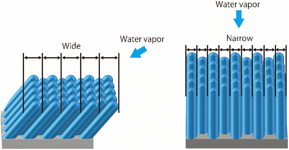 | ||
| Fig. 6 Simple morphological model of the columnar structure viewed from different directions. Arrows indicate the deposition directions of water vapor. The lateral size of surface irregularity along the y axis becomes larger than that along the x axis. | ||
Fig. 7(a) and (b) show the topographic images of the same area obtained at different times at 100 K. No substantial time variations were observed in the morphology or in the results of the HHCF analysis over 590 min, even in the case of T/Tm = 0.37. These results indicate that water molecules on ASW do not substantially diffuse enough within the timescale of several hours at 100 K to change the morphology in the scale of the observation area. That is, the morphology at 100 K is not determined by the thermal diffusion of the water molecules.
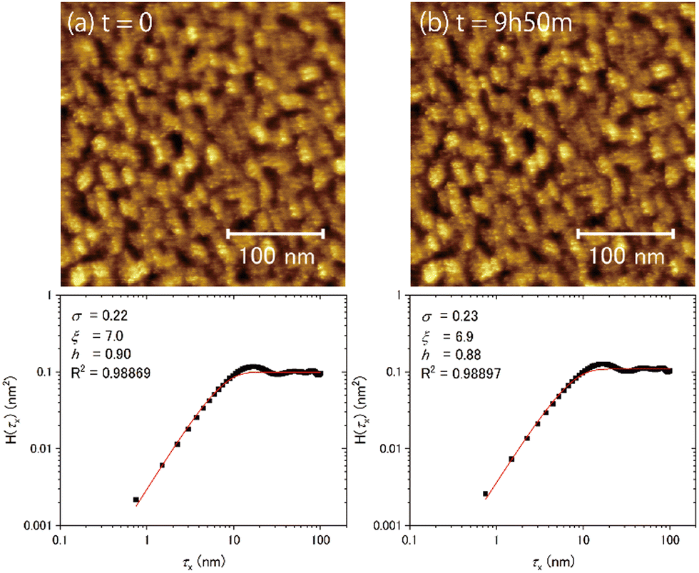 | ||
| Fig. 7 Topographic images of ASW at 100 K observed at the identical area. Image (b) was obtained 9 h 50 min after the acquisition of image (a). The HHCF analysis was applied to the x direction (perpendicular to the deposition direction). No substantial difference was observed between these images and the results of the HHCF analysis. | ||
This result implies that the morphology of ASW formed below at least 100 K is governed by the adsorption process of deposited water molecules until they stabilise because of energy dissipation. Water molecules on the surface of ASW exhibit five types of bonding with bulk ice: two- and three-coordinated bonding with a dangling hydrogen, two- and three-coordinated bonding with a dangling oxygen, and four-coordinated bonding with a modified tetrahedral structure.42 The abundance ratio of each bond type for surface water molecules is expected to vary depending on the vapor-deposition temperature of the ASW sample. Indeed, it has been reported that the integrated infrared absorbance of band strength corresponding to dangling OH bonds assigned to two- and three-coordinated surface molecules decreases with increasing vapor-deposition temperature.29 Differences in the bond structure of water molecules on the ice surface may influence morphology variations by affecting the energy dissipation of landing water molecules during transient diffusion. Clements et al.12 performed kinetic Monte Carlo calculations and found that the temperature dependence of the ASW densities observed in experiments can be explained by considering nonthermal diffusion (transient surface diffusion), which occurs during the dissipation of the adsorption energy. These results suggest that the adsorption dynamics of deposited water molecules is important for understanding the morphology of ASW.
Measurement of the local contact potential difference between the tip and the ASW surface
We observed the distribution of the local contact potential difference between the tip and the ASW surface at 400 measurement points evenly spaced within the topographic images shown in Fig. 8(a) for 15 K and Fig. 8(e) for 100 K, respectively. These topographic images were obtained at constant voltages of 1700 mV for 15 K and 100 mV for 100 K to achieve sharp imaging. The larger bias voltage required at 15 K compared with that required at 100 K is attributed to the larger negative surface potential of ASW at 15 K than at 100 K. This temperature dependence on the negative surface potential of ASW is consistent with the results of Kelvin probe experiments.28,29Fig. 8(b) and (f) present the height profiles at Fel = 0, while Fig. 8(c) and (g) present the local contact potential difference on ASW at 15 K and 100 K, respectively. Note that the values in these figures show the relative values (ΔHeight and ΔVLCPD), where the minimum height and the maximum VLCPD were both set to be zero. The variations of the ΔVLCPD in Fig. 8(c) and (g) clearly show that the VLCPD varied at each measurement point. If the negative surface potential could be scaled by the ASW thickness, the color distributions in figures of ΔHeight and ΔVLCPD should be equivalent at each temperature (hereafter, indicating positive correlation). However, various relationships between ΔHeight and ΔVLCPD were observed, as indicated by the black and white squares for the inverse and positive correlations, respectively. The plots of ΔHeight vs. ΔVLCPD in Fig. 8(d) and (h) show no clear correlation, indicating that the VLCPD cannot be simply scaled by the film thickness, unlike the macroscopic measurement of VCPD.28,29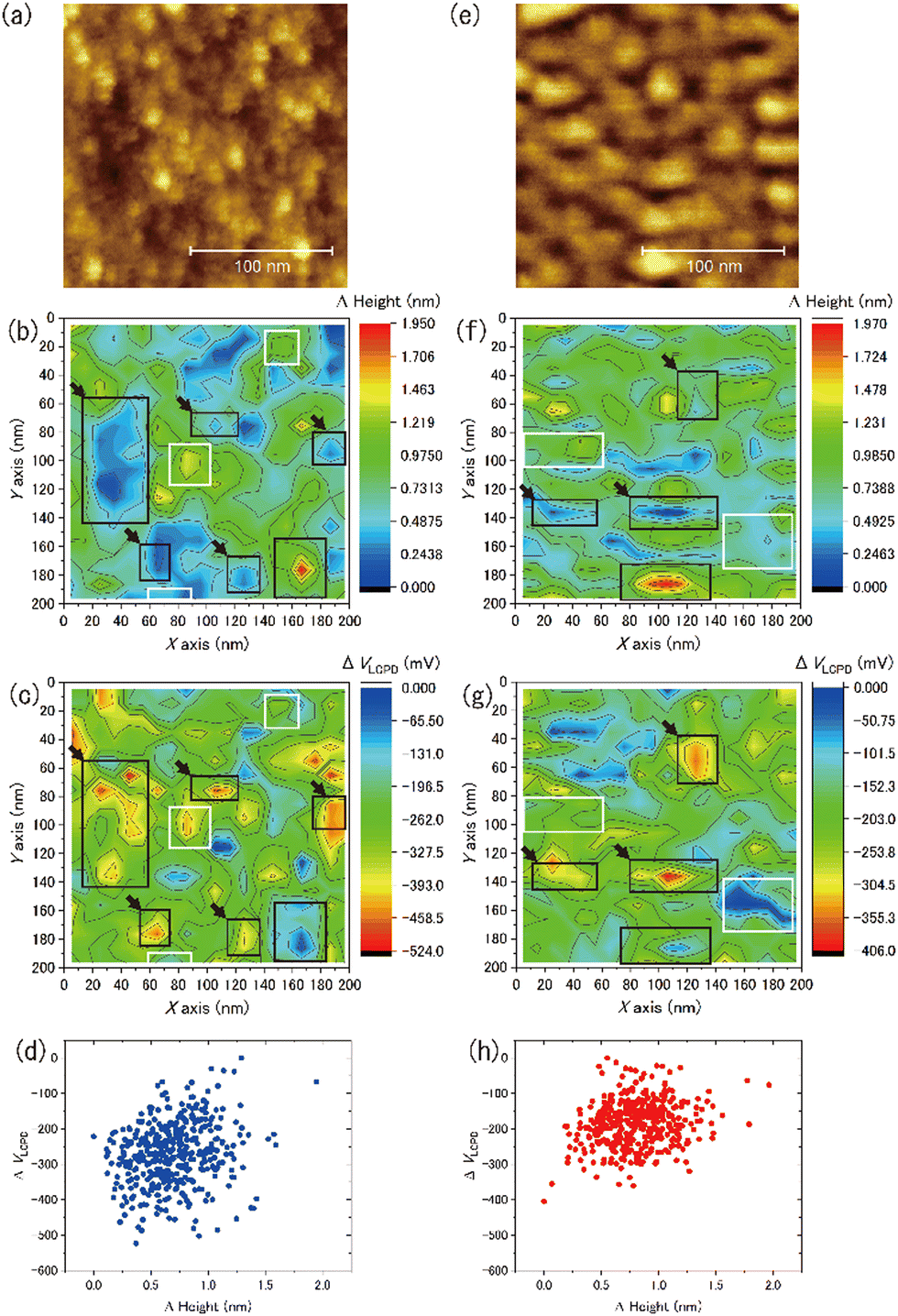 | ||
| Fig. 8 Topographic images of 13.5 nm-thick ASW at (a) 15 K and (e) 100 K, as observed using a constant bias voltage of 1700 and 100 mV, respectively. Relative height profiles of ASW at (b) 15 K and (f) 100 K, under the condition that the electrostatic force is cancelled (Fel = 0) by controlling the bias voltage at each measurement point. The relative local contact potential difference between the tip and the ASW surface at (c) 15 K and (g) 100 K at each measurement point. In panels (b) and (c) and (f) and (g), the black and white squares indicate areas where negative and positive correlations, respectively, are observed between the relative height and the negative amplitude of the relative contact potential difference. Plots representing the relationship between the relative height and the relative local contact potential difference at (d) 15 K and (h) 100 K. The black arrows indicate areas with a large negative surface potential at the pore. | ||
The tilted dipole (TD) model has been proposed by Bu et al.29 as a polarisation model for ASW. In this model, the polarisation of ASW is elucidated as arising from the orientation of water molecules within two- and/or three-coordinated bonding states at the pore surface (i.e., side walls of columnar structures). Specifically, the dipole moments of these water molecules align weakly, resulting in a positive end pointing toward the substrate. That is, the amplitude of the negative VLCPD at each measurement point is determined not only by the local thickness but also by the pore circumstances around measurement points. If the measurement point is located on the pore, a larger negative VLCPD will be observed even if the height of the ice surface at the pore is lower. This microscopic description of the polarisation model of ASW by the TD model is consistent with our measurement results, which do not show a positive correlation between the relative height and the relative amplitude of the VLCPD for the negative direction. In fact, substantial negative values of ΔVLCPD are observed at the deep pore sites at both temperatures (as indicated by the areas with black arrows in Fig. 8(c) and (g)), suggesting successful microscopic observation of the polarisation phenomenon of ASW proposed by the TD model. The smaller variations of ΔVLCPD at 100 K, shown in Fig. 8(h), compared to those at 15 K, shown in Fig. 8(d), can also be understood by considering that the transient diffusion of water molecules at 100 K caused a more homogeneous pore structure than that at 15 K.
Conclusions
In the present study, we used ultra-high vacuum cryogenic AFM to visualise the surface morphology and distribution of the local contact potential difference of ASW formed by water vapor deposition at 15 and 100 K on a Si(111)7 × 7 substrate. The typical lateral size of the surface structure in the topographic images of ASW was 5–10 nm at 15 K and 10–30 nm at 100 K. By contrast, the surface roughness was greater at 15 K than that at 100 K, indicating that the surface at 100 K exhibited a relatively flat morphology. The results indicated that HHCF analysis performed both perpendicular (i.e., in the x direction) and parallel (i.e., in the y direction) to the direction of water vapor deposition on the obtained topographic images enabled the ASW structure to be estimated. In addition, the distribution of the local contact potential difference on the ASW surface indicates that the local value of negative surface potentials is not simply proportional to the geometrical height (thickness). This result implies that the local structure of ASW affects the value of the local negative surface potential. The present results, where significant negative surface potentials were observed at measurement points on the ice pores, clearly demonstrate that the structure of ASW is related to the polarisation phenomena, which are the root of the negative surface potential observed on ASW. This result is also consistent with the TD model, which explains the negative surface potential as arising from the orientation of water molecules at the pore surface, which is proposed as the polarisation mechanism of ASW.The visualised data showing the surface morphology and the distribution of local contact potential differences of ASW can serve as variable comparative data for improving realistic simulation models for the formation of ASW. Visualising the morphological changes induced by external stimuli such as annealing and irradiation with UV photons would be important in understanding the chemical reactions on the surface of ASW and the sticking of ASW grains in protoplanetary disks. These topics will be the focus of future work.
Conflicts of interest
There are no conflicts to declare.Acknowledgements
This work was supported by the JSPS Grant-in-Aid for Specially Promoted Research (grant number: JP17H06087), the JSPS Grant-in-Aid for Transformative Research Areas (grant number: JP20H05849) and the Grant for Joint Research Program of the Institute of Low Temperature Science, Hokkaido University. We thank the staff of the Technical Division at the Institute of Low Temperature Science for fabricating the experimental devices. We are also grateful to Prof. Y. Sugimoto for advice on the experiments.References
- T. Hama and N. Watanabe, Chem. Rev., 2013, 113, 8783–8839 CrossRef CAS PubMed.
- E. Herbst and E. F. van Dishoeck, Annu. Rev. Astron. Astrophys., 2009, 47, 427–480 CrossRef CAS.
- C. Dominik and A. G. G. M. Tielens, Astrophys. J., 1997, 480, 647–673 CrossRef CAS.
- S. Okuzumi, H. Tanaka, H. Kobayashi and K. Wada, Astrophys. J., 2012, 752, 106 CrossRef.
- N. Miyauchi, H. Hidaka, T. Chigai, A. Nagaoka, N. Watanabe and A. Kouchi, Chem. Phys. Lett., 2008, 456, 27–30 CrossRef CAS.
- S. Ioppolo, H. M. Cuppen, C. Romanzin, E. F. van Dishoeck and H. Linnartz, Astrophys. J., 2008, 686, 1474–1479 CrossRef CAS.
- A. G. Dirks and H. J. Leamy, Thin Solid Films, 1977, 47, 219–233 CrossRef CAS.
- G. A. Kimmel, Z. Dohnálek, K. P. Stevenson, R. S. Smith and B. D. Kay, J. Chem. Phys., 2001, 114, 5295–5303 CrossRef CAS.
- Z. Dohnálek, G. A. Kimmel, P. Ayotte, R. S. Smith and B. D. Kay, J. Chem. Phys., 2003, 118, 364–372 CrossRef.
- S. Cazaux, J.-B. Bossa, H. Linnartz and A. G. G. M. Tielens, Astron. Astrophys., 2015, 573, A16 CrossRef.
- S. R. Hashemi, M. R. S. McCoustra, H. J. Fraser and G. Nyman, Phys. Chem. Chem. Phys., 2022, 24, 12922–12925 RSC.
- A. R. Clements, B. Berk, I. R. Cooke and R. T. Garrod, Phys. Chem. Chem. Phys., 2018, 20, 5553–5568 RSC.
- D. E. Brown, S. M. George, C. Huang, E. K. L. Wong, K. B. Rider, R. S. Smith and B. D. Kay, J. Phys. Chem., 1996, 100, 4988–4995 CrossRef CAS.
- B. A. Seiber, B. E. Wood, A. M. Smith and P. R. Müller, Science, 1970, 170, 652–654 CrossRef CAS PubMed.
- M. S. Westley, G. A. Baratta and R. A. Baragiola, J. Chem. Phys., 1998, 108, 3321–3326 CrossRef CAS.
- T. Loerting, M. Bauer, I. Kohl, K. Watschinger, K. Winkel and E. Mayer, J. Phys. Chem. B, 2011, 115, 14167–14175 CrossRef CAS PubMed.
- J. A. Ghormley, J. Chem. Phys., 1967, 46, 1321–1325 CrossRef CAS.
- E. Mayer and R. Pletzer, Nature, 1986, 319, 298–301 CrossRef CAS.
- K. P. Stevenson, G. A. Kimmel, Z. Dohnálek, R. S. Smith and B. D. Kay, Science, 1999, 283, 1505–1507 CrossRef CAS PubMed.
- B. Maté, Y. Rodríguez-Lazcano and V. J. Herrero, Phys. Chem. Chem. Phys., 2012, 14, 10595–10602 RSC.
- M. Mehlhorn and K. Morgenstern, Phys. Rev. Lett., 2007, 99, 246101 CrossRef PubMed.
- S. Maier, B. A. J. Lechner, G. A. Somorjai and M. Salmeron, J. Am. Chem. Soc., 2016, 138, 3145–3151 CrossRef CAS PubMed.
- K. Thürmer and N. C. Bartelt, Phys. Rev. B: Condens. Matter Mater. Phys., 2008, 77, 195425 CrossRef.
- J. M. K. Donev, Q. Y. B. R. Long, R. K. Bollinger and S. C. Fain Jr., J. Chem. Phys., 2005, 123, 044706 CrossRef CAS PubMed.
- H. Ueda, N. Watanabe, T. Hama and A. Kouchi, Phys. Rev. Lett., 2016, 116, 253201 CrossRef PubMed.
- T. Sugimoto and K. Fukutani, Nat. Phys., 2011, 7, 307–310 Search PubMed.
- A. Cassidy, M. R. S. McCoustra and D. Field, Acc. Chem. Res., 2023, 56, 1909–1919 CrossRef CAS PubMed.
- M. J. Iedema, M. J. Dresser, D. L. Doering, J. B. Rowland, W. P. Hess, A. A. Tsekouras and J. P. Cowin, J. Phys. Chem. B, 1998, 102, 9203–9214 CrossRef CAS.
- C. Bu, J. Shi, U. Raut, E. H. Mitchell and R. A. Baragiola, J. Chem. Phys., 2015, 142, 134702 CrossRef PubMed.
- F. J. Giessible, Rev. Sci. Instrum., 2019, 90, 011101 CrossRef PubMed.
- Kelvin Probe Force Microscopy, ed. S. Sadewasser and T. Glatzel, Springer, Heidelberg, 2012, p. 7 Search PubMed.
- S. K. Sinha, E. B. Sitrota, S. Garoff and H. B. Stanley, Phys. Rev. B: Condens. Matter Mater. Phys., 1988, 4, 2297–2311 CrossRef PubMed.
- T. Gredig, E. A. Silverstein and M. P. Byrne, J. Phys.: Conf. Ser., 2013, 417, 012069 CrossRef CAS.
- D. Nečas and P. Klapetek, Cent. Eur. J. Phys., 2012, 10, 181–188 Search PubMed.
- J. Krim and J. O. Indekeu, Phys. Rev. E: Stat. Phys., Plasmas, Fluids, Relat. Interdiscip. Top., 1993, 48, 1576–1578 CrossRef CAS PubMed.
- S. Labat, C. Guichet, O. Thomas, B. Gilles and A. Marty, Appl. Surf. Sci., 2002, 188, 182–187 CrossRef CAS.
- J. A. Thoruton, Annu. Rev. Mater. Sci., 1977, 7, 239–260 CrossRef.
- K. Robbie, J. C. Sit and M. J. Brett, J. Vac. Sci. Technol., B, 1998, 16, 1115–1122 CrossRef CAS.
- C. Buzea, K. Kaminska, G. Beydaghyan, T. Brown, C. Elliott, C. Dean and K. Robbie, J. Vac. Sci. Technol., B, 2005, 23, 2545–2552 CrossRef CAS.
- R. N. Tait, T. Smy and M. J. Brett, Thin Solid Films, 1993, 226, 196–201 CrossRef CAS.
- R. Alvarez, C. Leopez-Santos, J. Parra-Barranco, V. Rico, A. Barranco, J. Contrino, A. R. Gonzalez-Elipe and A. Palero, J. Vac. Sci. Technol., B, 2014, 32, 041802 CrossRef.
- J. P. Devlin and V. Buch, J. Phys. Chem., 1995, 99, 16534–16548 CrossRef CAS.
Footnote |
| † Electronic supplementary information (ESI) available. See DOI: https://doi.org/10.1039/d3cp05523j |
| This journal is © the Owner Societies 2024 |