
Charge carrier traps in organic semiconductors: a review on the underlying physics and impact on electronic devices
Hamna F.
Haneef
 ,
Andrew M.
Zeidell
and
Oana D.
Jurchescu
*
,
Andrew M.
Zeidell
and
Oana D.
Jurchescu
*
Department of Physics and Center for Functional Materials, Wake Forest University, Winston Salem, NC 27109, USA. E-mail: jurchescu@wfu.edu
First published on 17th December 2019
Abstract
The weak intermolecular interactions inherent in organic semiconductors make them susceptible to defect formation, resulting in localized states in the band-gap that can trap charge carriers at different timescales. Charge carrier trapping is thus ubiquitous in organic semiconductors and can have a profound impact on their performance when incorporated into optoelectronic devices. This review provides a comprehensive overview on the phenomenon of charge carrier trapping in organic semiconductors, with emphasis on the underlying physical processes and its impact on device operation. We first define the concept of charge carrier trap, then outline and categorize different origins of traps. Next, we discuss their impact on the mechanism of charge transport and the performance of electronic devices. Progress in the filed in terms of characterization and detection of charge carrier traps is reviewed together with insights on future direction of research. Finally, a discussion on the exploitation of traps in memory and sensing applications is provided.
1. Introduction
The promise of low-cost manufacturing, ease of processing, mechanical flexibility and versatility in chemical synthesis make organic semiconductors (OSCs) very attractive as components in electronic and opto-electronic devices. Examples include organic field-effect transistors (OFETs), organic light-emitting diodes (OLEDs), organic photovoltaics (OPV) and sensors.1–6 OSCs consist of conjugated molecules containing delocalized electrons resulting from the overlap of π-orbitals. The spatial overlap between the molecular orbitals of adjacent molecules determines the intermolecular electronic coupling and thereby the mechanism of charge transport.5,7–9 The intermolecular interactions in the condensed state are weak, mainly consisting of van der Waals forces, as opposed to the covalent and ionic bonds prevalent in inorganic solids. As a result, the processing requirements, as well as the mechanical, optical and electronic properties of OSCs, differ considerably from conventional crystalline or elemental semiconductors.4,10,11 Binding energies in OSCs are typically low (∼10 kcal mol−1, for reference, in crystalline Si (c-Si) the energy is ∼80 kcal mol−1),12 which makes them attractive for printable electronic applications.1 Their mechanical properties, coupled with manufacturing in ambient conditions, render them compatible with flexible substrates such as plastic, enabling their use in applications like bioelectronics, display technologies and wearable electronics.OSCs are clearly exciting materials, providing a wealth of technologically attractive properties and intriguing platforms to explore new science, but there are still many unanswered questions and challenges that need to be addressed before their widespread adoption. For example, charge carrier mobilities in OSCs rarely exceed 10 cm2 V−1 s−1, a value which is orders of magnitude lower than in c-Si or graphene, where mobilities in the order of 103 cm2 V−1 s−1 and 106 cm2 V−1 s−1, respectively, have been reported.13 The main reason for such low mobilities is the localization of charge carriers, a phenomenon that alters the already narrow bands resulting from van der Waals intermolecular interactions. In the early years of research on organic electronics (1950's), localization of charge carriers in molecular crystals was attributed to polarization whereby charge carriers interact with the surrounding electrons and nuclei in the lattice to form self-localized ‘polarons’.14 The transport of polarons was modelled using the polaron band theory and small polaron theory.15 Most crystalline OSCs measured in the nineties showed activated transport, which led to the wide acceptance of hopping as the dominant charge transport mechanism in OSCs.12,15 Later, observations of power-law temperature dependence of mobilities in high quality single crystals, which is reminiscent of band (delocalized) charge transport, challenged these theories.15 In the semi-classical description, band transport implies that charge carriers are delocalized over large distances compared to the lattice spacing and are only occasionally scattered by impurities and lattice vibrations. In OSCs however, delocalization of charge carriers is limited to a few molecules, hence the term ‘band-like’ was introduced to describe charge transport in these materials.16 Despite the observation of band-like transport, the mean free path of charge carriers in OSCs is comparable, and sometimes even lower than the intermolecular spacing, supporting localization of charge carriers and consequently low mobilities. This was a rather puzzling contradiction which piqued the interest of the scientific community. Recently it has been shown that dynamic disorder caused by large amplitude thermal motions of molecules is the main factor that limits the mobilities down to a few tens of cm2 V−1 s−1.13 This type of localization is short lived (transient localization) and survives only up to the timescale of the molecular vibrations, which in turn, can be suppressed at sufficiently low temperatures. New models based on a combination of quantum and classical dynamic concepts have been proposed to reconcile the coexistence of band-like/localized charge carriers and establish a proper theory to describe charge transport in OSCs.13,17
Localization of charge carriers can be caused by other sources of disorder such as chemical impurities and structural defects (static disorder). In addition, these sources can lead to the formation of electronic states in the band gap of the OSC. These in-gap states can subsequently trap charge carriers and hinder their transport, further preventing the OSC from realizing their intrinsic mobilities. Charge carrier trapping is a ubiquitous phenomenon that has repercussions on the performance and stability of OSCs and opto-electronic devices, as well as on our ability to access their intrinsic properties. Understanding the mechanisms and processes related to trap formation, the dynamics and timescales over which these processes occur is decisive in extracting fundamental performance limits of OSCs and subsequently engineering high-performance devices. This article aims to provide a comprehensive and timely review on the phenomenon of charge carrier trapping in OSCs, with emphasis on its impact on device operation. Starting with the definition of traps in Section 2, we continue by describing the different origins of traps in OSCs (Section 3), followed by a discussion on the effect of traps on the performance of organic opto-electronic devices (Section 4) and on the mechanism of charge transport in OSCs (Section 5). An overview of the experimental techniques available to detect and characterize traps will be provided in Section 6. Charge carrier traps can also be viewed as an opportunity for advanced detection: in Section 7, we discuss the exploitation of traps for organic-electronics-based sensing and memory applications.
2. What are charge carrier traps?
Before we move onto the description of traps, we introduce the density of states (DOS) function, which describes the energetic distribution of electronic states within energy bands. In a perfectly-ordered, crystalline semiconductor, such as c-Si, the density of delocalized (extended) states takes the form of a lying parabola (E1/2 dependency, where E is the energy of an electronic state) with well-defined band edges and hence a band gap (see Fig. 1a).18 In semiconductors with weak localization, such as amorphous Si (a-Si), the extended states tail into the band gap to create localized states as shown in Fig. 1b.19 These tail states are often modelled by an exponential function.20,21 In this case, an energy gap and band edges cannot be precisely defined; instead a mobility-edge that separates extended states from localized states was introduced.19,22 In disordered semiconductors, the localization is strong and the DOS is typically approximated with a Gaussian distribution (Fig. 1c) or an exponential distribution (Fig. 1d).20,23 The highest occupied molecular orbital (HOMO) and the lowest unoccupied molecular orbital (LUMO) are analogous to the top of the valence band and bottom of the conduction band, respectively. These terms will be used interchangeably throughout this review. For a Gaussian shaped DOS, an effective transport energy is defined as the energy at which a charge carrier equilibrates over time after multiple hopping between the localized states.19,24 The onset of the HOMO and LUMO are defined at the onset of the Gaussian when the tangent through the inflection point crosses the baseline (see Fig. 1c).11,19 Depending on the extent of localization of charge carriers, which is decided by various factors such as the molecular structure, molecular packing and the extent of disorder, the shape of the DOS function can be approximated to one of the four forms illustrated in Fig. 1. Ideal, perfectly-ordered single crystals adopt the DOS shape in Fig. 1a; however, the disorder induced by thermal molecular motions (discussed in Section 3.1) gives rise to tail states in the band gap and therefore their DOS is better approximated by the curve in Fig. 1b.13,25–27Fig. 1c and d are typically used to represent the DOS in polycrystalline and amorphous OSC films.11,20,23,28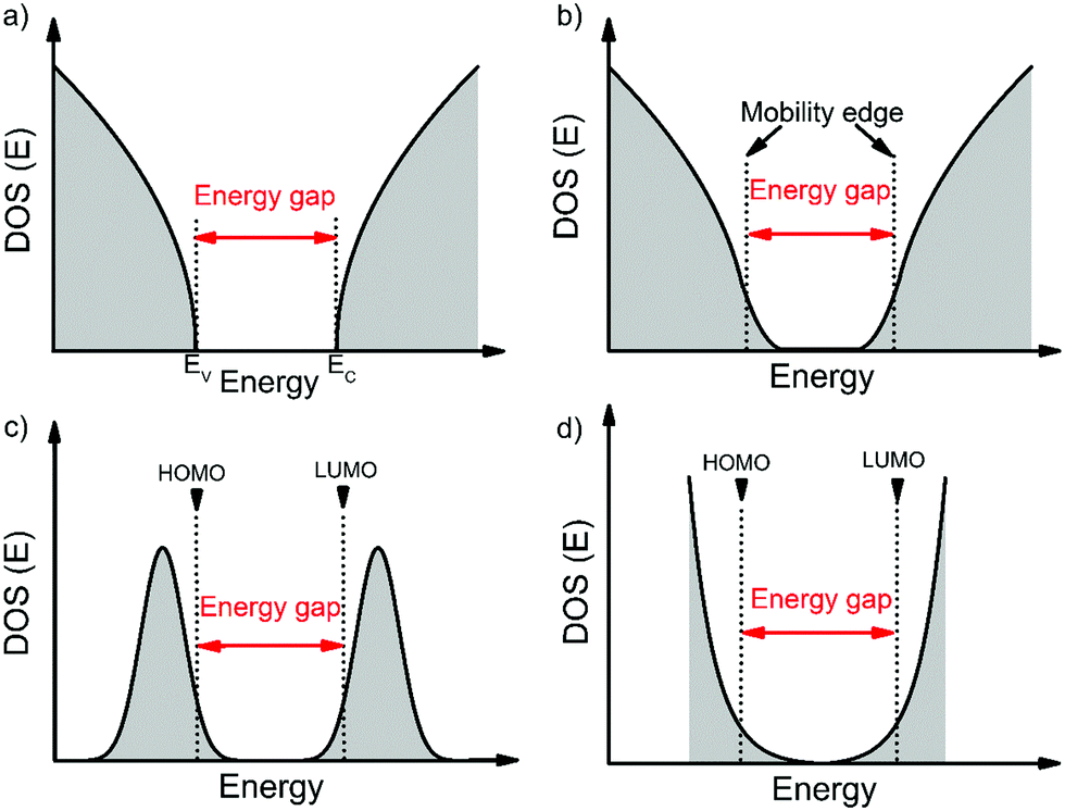 | ||
| Fig. 1 Extended states DOS function of (a) crystalline OSCs, (b) crystalline OSCs with weak localization, and (c), (d) polycrystalline/amorphous OSCs assuming Gaussian and exponential models, respectively. | ||
An electronic trap is any imperfection in the semiconductor that creates localized electronic states spatially distributed around the site of the imperfection and energetically distributed within the band gap of the semiconductor. Depending on their relative energetic positions from the band edge (trap depth) at a given temperature, traps can be shallow if located in the vicinity (a few kT) of the band edges, or deep if they lie further (several kT) from the band edges as illustrated in Fig. 2, where k is the Boltzmann's constant and T the temperature. Localized tail states in the band gap are generally considered shallow traps, with acceptor-like states near the LUMO edge and donor-like states near the HOMO edge representing trap states for holes and electrons, respectively. A trap can capture and restrain a charge carrier temporarily until it is released back into the band by an external stimulus such as electric field, thermal energy or a photon. For example, in the multiple-trap and release (MTR) model, charges moving within delocalized states are trapped by a localized shallow trap state in the band gap, then released back into the energy band by thermal energy as depicted by the blue arrows in Fig. 2.29,30 A band-like motion (which occurs within delocalized states) is also illustrated in Fig. 2, in black arrows, for comparison. If the trap densities are high, trapped charge carriers can participate in transport through thermally-activated hopping or tunneling from one localized state to another (orange arrows in Fig. 2).31 Thermal detrapping of charge carriers is possible if the trap depth is sufficiently low (∼kT); charge carriers residing in shallow traps at a given temperature are more likely to get thermally excited back into the band, while those in a deep trap have a negligible probability of being thermally excited.32 Such deep states often act as recombination centers for charge carriers reducing their overall lifetime.
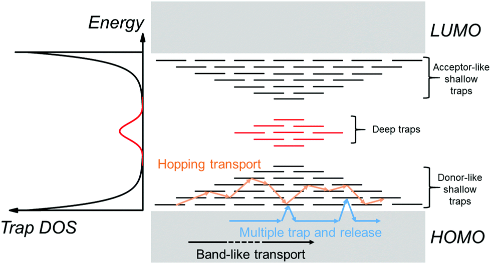 | ||
| Fig. 2 (left) The trap DOS function represents shallow traps resulting from tail states (black) and deep traps (red) in the band gap. (right) Schematic spatial and energy diagram of an OSC containing localized trap states in the bad gap. Tail states forming acceptor-like and donor-like shallow traps are shown in black, while deep traps are shown in red. Arrows represent different transport regimes possible in an OSC; band-like transport (black), MTR (blue) and thermally-activated hopping transport between localized states (orange). | ||
A DOS function to represent localized electronic states within the band gap of an OSC can be defined. Such a function is referred to as trap DOS. Traps can have discrete energy levels or a quasi-continuous energy distribution that is often described using an exponential or a Gaussian function.33–36 The left panel of Fig. 2 illustrates a Gaussian distribution of trap states deep in the band gap (red curve) in addition to the disorder-induced tail states (black curve) extending into the band gap, and which act as shallow traps.
3. Sources of traps in organic semiconductors
Electronic traps in OSCs can originate from varying sources, as summarized in the scheme in Fig. 3. The main source of traps in OSCs is disorder. Structural defects and chemical impurities cause static disorder and are considered intrinsic sources of traps in OSCs. They form during or after crystal/film formation and can be minimized through careful control of the growth process. In addition, dynamic disorder is an intrinsic source of traps. Extrinsic traps can be intentionally or unintentionally introduced by either exposure to gases, electromagnetic radiation, temperature gradients, bias stress, dopants, or by interfacing with other materials such as a metal, dielectric or another OSCs. Since the energetic landscape involved in the presence of inadvertent chemical impurities and deliberately added dopants is similar, dopants will be discussed in the context of chemical impurities. In this section, we will discuss each type of traps included in the scheme and will provide examples on how they impact material and device properties.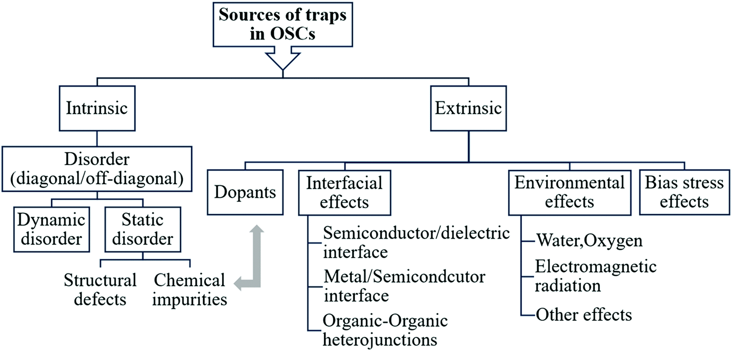 | ||
| Fig. 3 Sources of charge carrier traps in OSCs. | ||
3.1. Disorder
Perturbations or imperfections in the crystal structure, existing either in a single unit cell or extending over several unit cells, can locally destroy the crystal and translational symmetry, thereby introducing disorder into the system. The spatial distribution of structural properties such as intermolecular electronic coupling results in structural disorder, also called off-diagonal disorder.8 If the disorder translates into fluctuations in site energy (i.e., HOMO or LUMO energy level) of a molecule or molecular segment, it is referred to as energetic disorder or diagonal disorder.8 Any structural disorder in the cartesian domain will inevitably give rise to energetic disorder in the energy domain.24 Energetic disorder is often modelled by a Gaussian distribution of energy with a standard deviation quantifying the extent of disorder.37 An exponential DOS is also used to model disorder-induced tail states in the band gap.20,21The disorder can be dynamic or static: dynamic disorder is caused by thermal motions of the molecules (intermolecular and intramolecular), i.e. from electron–phonon interactions, while static disorder is caused by structural defects (Section 3.1.1) and chemical impurities (Section 3.1.2). The major difference between the two is that the former results in time-dependent variations in the site energies and transfer integrals and occurs throughout the entire crystal, while the latter is time-independent and occurs only at specific locations where the defects are present. Dynamic disorder can destroy the already narrow electronic energy bands, resulting in localization of charge carriers. However, the disorder lasts only up to the timescale of the thermal motions (hence the term ‘transient localization’) and can be sufficiently reduced at low temperatures.13 Static disorder can also result in charge carrier localization (Anderson localization) arising from the variations in electron potentials.38 Both dynamic disorder and static disorder introduce localized tail states in the band gap, with the latter creating additional in-gap states due to the presence of structural inhomogeneities. Tail states induced by dynamic disorder form even in nominally perfect OSC single crystals and represents the major performance limiting factor in such materials.27,39 Moreover, the density of tail states resulting from large amplitude thermal motions is much higher than those resulting from structural inhomogeneities, and hence they play a key role in determining the details of charge transport in materials in which the electronic coupling between molecules is weaker compared to the electron–phonon coupling.40 A discussion on the effect of disorder on charge transport is beyond the scope of this review and the reader is directed to the rich literature existing on the subject.8,13,17,37,41–43 In this review, the discussion will be limited to the disorder-induced gap states that can potentially trap charge carriers. Theoretical calculations confirmed the existence of a tail of gap states near the valence band edge resulting from thermal molecular motions.25,44–46 In pentacene, for example, the states were modelled exponentially to yield a tail breadth of 6.9 meV at 100 K, increasing to 12.7 meV at 300 K due to higher amplitude thermal motions at elevated temperatures.25 By using a combination of temperature-dependent FET and charge modulation spectroscopy (CMS) measurements, Sirringhaus and coworkers confirmed that dynamic disorder induces shallow traps.47 They found that the degree of localization is sample dependent and charge carriers are highly localized in pentacene films, a phenomenon that does not occur in 2,8-difluoro-5,11-bis(triethylsilylethynyl) anthradithiophene (diF-TES ADT), even at low temperatures. Band gap tail states have been experimentally observed in several materials such as single crystals of rubrene and their derivatives, but their precise origin remains unclear.48,49 Troisi and co-workers pointed out that they are similar to those detected in inorganic semiconductors which result from intrinsic electronic disorder.15 Experimental evidence on the presence of gap-states due to static disorder and their role in charge carrier trapping will be provided in the succeeding Sections 3.1.1 and 3.1.2.
Dislocations in molecular crystals have been studied since the early 70's.33,51–54 Thomas and Williams showed that in anthracene crystals molecules residing within ca. 400 Å radius from the site of dislocation act as traps for holes.52 Dislocations in naphthalene crystals have been identified by Lohman and Wehl as electron traps.53 The density of dislocations mainly depends on the growth technique; vapor-grown crystals typically have a lower dislocation density compared to crystals grown from the melt or solution.52 In addition to being a charge trapping site by itself, edge dislocations readily accommodate impurities around their core, potentially creating additional trapping states.52
Step edges were identified as electron traps in single crystals of N,N′-bis-(heptafluorobutyl)-2,6-dichloro-1,4,5,8-naphthalene tetra-carboxylic diimide (Cl2-NDI) using scanning Kelvin probe microscopy (SKPM).55 It was found that the OFET threshold voltages and mobilities depended strongly on the density of step edges, with the former decreasing and the latter increasing with increased step densities.
Grain boundaries (GBs) present in OSC thin films add to structural defects within the grain and hamper charge carrier transport,56–61 although some exceptions exist.62 The discussion of whether they act as traps or energy barriers for charge carriers has been controversial, both phenomena resulting in thermally-activated transport.32,63 Spatially resolved techniques were adopted to access the local nature of trapping in polycrystalline thin films. Marohn and coworkers used electron force microscopy to study the spatial distribution of traps as a function of gate–source voltage in pentacene thin-film transistors.64–66 They found that the traps are not only concentrated on grain boundaries, but distributed throughout the film. On the other hand, using scanning probe microscopy measurements, Frisbie and coworkers observed that the surface electrostatic potential at GBs is lower than that in the crystallites, which indicates that holes are predominantly trapped at GBs.67 This result is in agreement with the work by Horowitz et al. and Sirringhaus and coworkers.68,69 Kaake et al. suggested that charge carriers are trapped within the grains, while the surrounding grain boundaries act as insulating barriers for the trapped charge carriers preventing them from crossing the grain boundaries.63 Their interpretation was based on the weaker electronic coupling between molecules located in grain boundaries compared to those located inside the grains, a phenomenon that pushes the HOMO and LUMO levels into the band rather than into the band gap and hence does not cause charge carrier trapping. Teague et al. detected a pronounced potential drop at GBs,70 in agreement with earlier studies which found an order of magnitude larger resistance across the grain boundaries than within the grains.71 The existence of different types of GBs resulting from different processing conditions, as indicated by Lee et al. and Jimison et al., might be the cause of such different responses.72,73
Structural defects in the form of stacking faults were detected in pentacene thin-films using a combination of electronic structure calculations and scanning tunneling microscopy.74 It was proposed that compressive stress during film growth causes the molecules to slide along their long-axis, leading to larger molecular overlap, which results in the formation of shallow traps with energies ≤100 meV close to the band edges. In solution deposited small molecule OSCs, this type of defect was healed by introducing gentle vibrations during crystallization, and a reduction in the density of trap states was confirmed by spectral analysis of the trap density of states.75 Line dislocations have been identified in pentacene thin films by using a combination of scanning probe microscopy and chemical etching.67
In polymers, conformational defects such as kinks in the backbone can introduce both shallow and deep trapping states.76,77 The kinks can break the conjugation and generate energetic disorder resulting in a sequence of conjugated segments each having different HOMO and LUMO levels. Synthesis routes to minimize the energetic disorder in amorphous polymers have been proposed. For example, the synthesis of the polymer poly(para-phenylene) (PPP) by planarization of the polymer backbone (ladder polymer) yielded well-defined conjugation length and interchain order resulting in high-performance OLEDs.77 In indacenodithiophene-benzothiadiazole (IDT-BT), a donor–acceptor copolymer that has gained a lot of attention lately for its high charge carrier mobilities,78 the performance is obtained in spite of its low crystallinity.79 These electrical properties that are approaching a trap-free limit result from an efficient transport along the rigid backbone, with occasional hopping through π-stacks. In fact, even though amorphous polymers lack long-range order, they contain ordered crystalline domains that obey the Physics of crystalline polymers.80 Karki et al. used solid state nuclear magnetic resonance (NMR) spectroscopy to quantify the relative densities of ordered and disordered regions of two structurally distinct polymer films highlighting the impact of the molecular structure on the degree of order.80
| Eht = IG − IH | (1) |
| Eet = AG − AH | (2) |
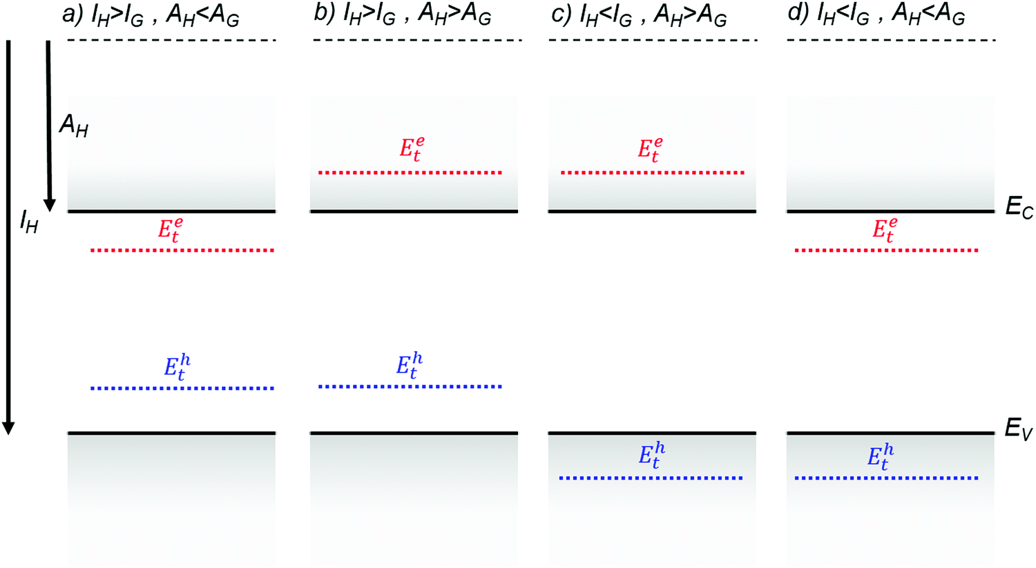
Fig. 4 illustrates several hypothetical situations in which charge carrier trapping or anti-trapping states are formed by the presence of guest molecules in a host lattice. In the first case (Fig. 4a), the HOMO and the LUMO levels of the guest are positioned within the band gap of the host, therefore generating trap states for both holes and electrons. For anthracene crystals doped with tetracene guest molecules, Karl showed that hole traps formed at 0.42 eV from the valence band edge and electron traps at 0.12–0.17 eV from the conduction band edge.81 An order of magnitude reduction in the hole mobilities was observed even with 0.5 ppm of tetracene as a result of the dominant hole trapping.82 The transport mechanism was band-like for the pristine crystal, as determined from time of flight measurements, and MTR for the crystal doped with tetracene. In Fig. 4b, the guest molecule introduces trap states only for holes, such as in the case of anthracene crystals doped with phenothiazine, where the trap was detected at 0.8 eV from the HOMO level using time of flight measurements.83 The example illustrated in Fig. 4c presents a chemical impurity with ionization energy greater than, and electron affinity less than those of the host. Such an impurity is energetically inert. Even though this type of impurity is not directly associated with charge carrier trapping, it still contributes to a local distortion of the lattice and can act as a scattering center for charge carriers. The concentration of the impurities or dopants will determine the total scattering events. Tetracene molecules in an anthracene host is such an example, where anti-traps for both electron and holes are formed.33,81,83 Finally, Fig. 4d describes the case when the guest molecule introduces trap states for electrons only. Using time of flight measurements, Karl detected electron trapping in anthracene crystals doped with acidine, phenazine and anthraquinone at energies 0.2 eV, 0.54 eV and 0.6 eV respectively from the conduction band edge.81
 | ||
| Fig. 4 Charge carrier trapping and anti-trapping states resulting from the presence of a guest molecule in a host lattice. Additional in-gap states are not shown for clarity. Solid lines represent the band edges of the host molecule and broken blue lines and red lines represent discrete tapping states for holes and electrons respectively. (a) Trap state for both holes and electrons, (b) trap state for holes and anti-trap state for electrons, (c) anti-trap state for both holes and electrons and (d) anti-trap state for holes and trap state for electrons. | ||
Chemical degradation can also lead to the formation of traps. Oxidation is one of the most common forms of degradation in OSCs. In the case of acene crystals, oxidation leads to the formation of quinones. In anthracene and tetracene crystals, the respective quinones form deep traps for electrons, as confirmed by photoemission measurements.33 Photo-oxidation of the crystals resulted in an increased concentration of such impurities. In pentacene single crystals, pentacenequinone acts as an energetically inert impurity, similar to the example included in Fig. 4c, but its presence lowers the charge carrier mobilities by locally distorting the lattice.84 Reduction of the impurity content by a factor of five led to two orders of magnitude lower trap density, and mobilities as high as 35 cm2 V−1 s−1. Environmental contaminants such as moisture (H2O) and O2 can also create discrete trap states. The high electron affinity of O2 gas molecules make them potential traps for electrons.85 Isolated H2O and O2 gas molecules cannot trap holes as their gaseous phase ionization energies are too high (∼12 eV).86 However, clusters of water molecules have significantly lower ionization energies due to stabilization of charge from the dipole moment of surrounding molecules and hence can form potential traps for holes.86,87 Examples of such traps will be discussed in Section 3.3.
Dopants are often added to OSCs to enhance their conductivity. The doping efficiency is governed by several factors such as the offset of energy levels between the host and the guest and the dopant concentration. The mechanism of charge transport in doped OSCs is complex and is dominated by several competing processes that depend on the above factors. For example, the addition of a dopant can either broaden the DOS of the host thereby introducing tail states, or the dopant-induced charge carries can fill up existent trap states to neutralize them or the presence of the dopant can annihilate the trap states.88–91 For a detailed description of doping in OSCs and different types of doping such as molecular and metallic doping, we recommend the review by Lüssem et al.92
3.2. Interfacial effects
Organic electronic devices consist of consecutive layers of dissimilar electronic materials and their architecture has different complexity levels depending on the function that they perform. The phenomena occurring at interfaces between any two distinct layers, such as electrode/semiconductor, semiconductor/dielectric and interface with other organic layers, add to the charge carrier trapping discussed in Section 3.1, which focused on the processes occurring in the bulk of the OSC. Trapping at interfaces has a profound impact on device performance, as we will describe in this section.Another route for trap generation at the semiconductor/dielectric interface is related to the adsorption of impurities such as water, oxygen or hydroxyl groups. The passivation of dangling bonds at the surface of the SiO2 gate-dielectric by adsorption of hydroxyl groups results in a high density of silanol groups at the surface that can trap electrons. This has been the main challenge in achieving electron transport in SiO2-based transistors.93,96 The application of self-assembled monolayers (SAMs) such as hexamethyldisilazane (HMDS), octadecyltrichlorosilane (OTS), and decyltrichlorosilane (DTS) has proven to passivate some, (but not all) of the surface traps in SiO2 to yield functional n-channel OFETs.96 Stable operation of the devices was realized with the use of polyethylene as a dielectric buffer layer.96 Fluorinated polymer dielectrics such as Cytop and poly[4,5-difluoro-2,2-bis(trifluoromethyl)-1,3-dioxole-co-tetrafluoroethylene] (AF2400) allow for a significantly lower interfacial trap density compared to SiO2.97,98 Also, the fluorine group renders them hydrophobic and hence they can repel water molecules,99,100 and when used as top gate dielectrics, they act as encapsulants.
The effect of the gate dielectric type on the performance of pentacene thin film transistors has been investigated by Knipp et al.101 The transfer characteristics was modelled by a trap DOS consisting of two exponential distributions of deep acceptor-like states and donor-like shallow states,20 with the former accounting for the onset of drain current while the latter accounts for a non-zero threshold voltage. The nature of the dielectric affected film microstructures which, in turn, determined the density and the depth of the trap DOS. For example, films on benzocyclobutane (BCB) consisted of smaller grains than those on SiO2 and yielded a more negative threshold voltage due to a broader distribution of donor-like shallow trap states, with the width increasing from 45 meV on SiO2 to 90 meV on BCB. Modification of film microstructure has also been achieved by treatment of the substrate with SAMs, leading to lower trap densities and therefore high charger carrier mobilities.102 SAMs such as OTS and octadecyltrichlorosilane (ODTS) provide a low-surface energy, which typically yields a better film morphology, but they are challenging to implement in solution-deposited devices.103,104
Mei et al. discovered that the mismatch in the coefficient of thermal expansion (CTE) of consecutive device layers induces strain at the interfaces, which results in generation of localized trapping states.105 They found a crossover from a band-like transport to a temperature activated-transport upon increasing the interfacial thermal expansion mismatch, which could not be explained by polaronic effects alone,106–108 and was assigned to charge trapping due to thermal strain.
The above effects arising at the semiconductor/dielectric interface vanish in the case of a transistor with a vacuum-gap dielectric, as demonstrated by Sundar et al. and Menard et al. using polydimethylsiloxane (PDMS) stamps as substrates.109,110 However, the CTE mismatch between the PDMS substrate and the OSC can introduce microstrain in the crystal, which in turn modifies its work function.111 Such modifications can potentially create band tail states induced by electrostatic disorder.
The surfaces of organic crystals are prone to contamination and defects and when a metal comes in contact with such a surface, localized states are induced at the interface between the two materials. These states introduce a surface potential which can subsequently increase the injection barrier. Baessler and Vaubel detected surface states in anthracene single crystals by measuring the threshold energies of photoemission of charge carriers from a variety of metals into the crystal.118 They found that high work function metals such as Mg and Pb did not affect the interface, while a surface potential was generated for low work function electrodes such as Ca, Na, Cs and Ba due to electron trapping. A surface trap density of 2 × 1012 cm−2 eV−1, with a maximum trap depth of 1.3 ± 0.2 eV was evaluated. de Boer and Morpurgo investigated this effect by comparing the results of space charge limited current (SCLC) measurements performed on tetracene single crystals in a sandwich structure, with the crystal laminated on a pre-fabricated Au contact (bottom contact), and the top Au contact deposited by electron-beam evaporation.119 In spite of the nominally identical electrode/OSC interfaces, they found that the injection was more efficient from the surface of the bottom contact. They concluded that the e-beam evaporation process damages the crystal surface due to interaction with X-rays and high energy electrons during the deposition process, resulting in a larger density of traps compared to the pristine bottom surface. The trap density at the crystal surface was also larger than that in the bulk, highlighting the effect of processing on the surface traps and, consequently, charge transport. This effect was further explored by Coll et al. and they developed a non-destructive deposition method for top contacts, i.e., flip-chip lamination.120 The technique was based on nano-transfer printing and involved the adhesion of ultra-smooth patterned contacts onto the organic crystal. This resulted in similar SCLC currents from both top and bottom electrodes confirming that flip-chip lamination preserves the crystal quality.
3.3. Environmental effects
Exposure to environment either during device fabrication, handling and/or characterization, often affects the quality of the OSC and can lead to trap formation. Temperature, moisture (H2O), ambient gases (O2) and electromagnetic radiation such as light and X-rays are some other possible sources of traps. Recent developments have led to very stable organic electronic devices, a milestone which has been realized through careful device and material design.121–124Traps related to temperature manifest themselves in OFETs as shifts in turn-on voltage Von, subthreshold slope S and threshold voltage Vth.125,126 The borderline between shallow and deep traps changes with temperature. i.e., at sufficiently high temperatures all traps behave as shallow traps and vice versa. Ambient moisture in pentacene films have been known to cause OFET device degradation, resulting in larger Vth, S, and high on-currents.127–130 Water molecules can either act as traps for charge carriers or cause redox reactions in the OSC.131 Using first-principle calculations, it was predicted that water-related defects are energetically favorable in pentacene and hence are more likely to occur.132 Such traps have led to bias stress instabilities in OFETs.124,133–135 In pentacene single crystal transistors, a discrete trap state with density up to 1012 cm−2 was generated during negative bias stress as a result of water adsorbed on the SiO2 dielectric.134 Gomes et al. investigated this effect as a function of temperature and discovered that bias-stress effects are only present above 200 K, which corresponds to a known phase transition of supercooled water.135 This was observed in several OSCs independent of deposition techniques. Bias stress effects due to water adsorbed by the dielectric can be minimized by rendering the dielectric hydrophobic either by using fluorinated polymers as dielectric,136 by the application of SAMs,134 by inserting interlayers between the dielectric and OSC,133 or by encapsulating the devices.137 Water-related traps in conjugated polymers has recently gained a lot of attention.87,124,138 Blom and coworkers, found that hydrated oxygen complexes form electron traps in polymeric electron-only diodes: transport is limited by traps exhibiting a Gaussian distribution centered at ca. 3.6 eV from the vacuum level with a density of 3 × 10²³ m−3 and a width of ∼0.1 eV.138 Zuo et al. used a similar approach to show that electron and hole traps created in hole-only and electron-only devices made of several OSCs were a result of water molecules enclosed in nanoscopic voids in the films.87 A peak was observed in the slope of the logarithmic current–voltage curve plotted as a function of voltage, which was assigned to a transition from trap-limited to trap-filled charge transport regime. By modeling the curves using a 1-D drift-diffusion model, hole and electron trap distributions were determined to be consistently centered around 0.3–0.4 eV from the HOMO and LUMO levels respectively, for all materials. Solvent-vapor annealing in a saturated o-xylene environment removed majority of water in the nanovoids through molecular rearrangements, resulting in suppression of the trapping peak. The study has recently been expanded to include small molecules, proposing a universal design rule to achieve trap-free bipolar transport in organic devices.86 Recently, Nikolka et al. investigated bias stress effects in conjugated polymers due to the existence of water molecules in the voids of the polymer films that act as charge carrier traps.124 They showed that incorporation of solvent additives or dopants displaces the water molecules and enhances the operational stability of the device.
Various types of oxygen-related traps in pentacene have been studied theoretically and experimentally.48,132,139,140 Northrup et al. predicted that trap states form when an H-atom is replaced with an O-atom that forms a double bond with the C-atom.139 Another possible defect, where an O-atom bridges two C-atoms of neighboring pentacene molecules, was predicted to generate trap states with energies in the range 0.33–0.4 eV above the valence band edge.132 Batlogg and coworkers studied the effect of oxygen on the trap DOS spectrum of pentacene thin-film transistors and found that a broad peak centered at 0.28 eV from the valence band edge, with a total volume density ∼1018 cm−3, was created. A similar peak was observed by Knipp et al. in pentacene films exposed to oxygen under a continuous bias stress.140 Density functional theory calculations suggested the formation of an oxygen-pentacene complex, which then creates a C–O bond with a neighboring pentacene molecule. The formation of the complex is facilitated by the applied gate-bias under oxygen exposure. Discrete trap states induced upon O2 exposure have also been observed in rubrene single crystals using temperature-dependent SCLC measurements, where a hole trapping state was resolved at 0.27 eV above the valence band edge.48
OSCs are inevitably exposed to ionization radiation such as X-rays during structural characterization, or even during operation. Several studies involving intentional exposure of ionizing radiation to elucidate its effect on device metrics and the DOS spectrum have been reported. Exposure of rubrene single crystals to X-rays caused shifts in Vth of the OFETs, but surprisingly the mobilities remained unharmed, suggesting that the generated traps are located deep in the bandgap.126 Rubrene crystals have also been exposed to He+ ions and their effect on the trap DOS was studied using temperature-dependent SCLC measurements.141 A discrete peak at 0.35 eV from the HOMO edge was resolved with trap densities (∼1016 cm−3) initially increasing with radiation dosage and saturating at higher dosages. The formation of the trap was attributed to C–H bond breaking and hydrogen loss.
4. Effect of charge carrier traps on electronic devices
The presence of traps in OSCs has a profound impact the performance of electronic devices. In this section, we briefly discuss such effects in OFETs, OLEDs and OPV devices. In OLEDs, electrons and holes emitted from opposite sides of the OSC recombine radiatively to emit light and traps can cause non-radiative recombination, thus reducing the efficiency of the devices.6,142,143 In addition to reducing the charge carrier mobilities, which also results in low efficiency, the presence of traps can cause device degradation.144,145 OPVs are based on organic–organic heterojunctions where electron–hole pairs (excitons) are generated from two different OSCs upon absorption of light. The excitons dissociate into free carriers at the heterojunction and are carried out separately to the external circuit. Traps can cause non-radiative Shockley–Read–Hall recombination of the dissociated charge carriers, decreasing the quantum efficiency of the devices.146,147 Traps also alter the energy level alignment at the organic–organic heterojunction.148–150 In addition to impacting the fill factor, the misalignment between the energy levels will directly influence the maximum achievable open-circuit voltage.149 On the other hand, traps can assist with the dissociation of excitons into free carriers.151 The excitons are bound together by high Coulomb energy which acts as an energy barrier for dissociation. The electrons and holes can dissociate down to lower energy states formed by traps and finally overcome the barrier, thereby increasing the efficiency of the devices.OFET technology holds great promise to realizing applications such as active matrix OLEDs, radio frequency identification (RFID) tags, electronic paper and sensor arrays. In addition, they offer a versatile platform for charge transport studies under different charge density regimes and an experimental tool for unambiguous determination of charge carrier mobilities. An important parameter that defines the electrical performance of OFETs is the mobility of the charge carriers in the transistor channel, μ, which represents the average speed at which the carriers move in the presence of an electric field. Trapped charge carriers reduce the effective mobility, with the density of traps and trapping timescale defining the macroscopic transport. In the presence of traps, the mobility is gate-voltage dependent.31,152,153 At low gate–source voltages, the injected/accumulated charges occupy the available trap states and the drain current is the result of charge transport occurring through thermally-activated hopping/tunneling between these states. As the gate-voltage increases, the trap states are gradually filled, and at sufficiently large voltages all states are filled and the charge carriers can finally occupy the extended states and subsequently increase the mobilities. The gate–source voltage required to fill trapping states before charge accumulation is possible in the transistor channel is called the threshold voltage and hence a non-zero threshold voltage is indicative of the presence of traps.152 In fact, the value of the threshold voltage provides direct access to the density of traps, as will be described in Section 6.1.2. However, other effects such as contact resistance and the gate-bias dependent charge carrier concentration in the channel, can also contribute to gate-voltage dependent mobilities.102,153–156 The presence of traps and contact resistance are competing effects that obscure device characteristics and it is often difficult to distinguish the effect of one from the other. Bittle et al. studied the effect of molecular ordering in regioregular poly(3-hexylthiophene) (RR P3HT) films on OFET characteristics.156 A reduction in contact resistance and a shift to field-independent mobilities occurred as a result of narrowing of the density of localized states near the band edge in films with increased crystalline order. Traps can also be manifested in the subthreshold region of the transfer characteristics, where the gate–source voltage is below the threshold voltage and the drain current has an exponential dependency on the gate voltage.4 Thermal de-trapping of charge carriers from shallow traps can contribute to high off currents, resulting in a less steep subthreshold region and a high subthreshold swing, S.157 Practical applications require very steep subthreshold swing for fast switching of devices with a theoretical limit of 60 meV at room temperature.4 Another salient feature in practical OFETs, resulting from the existence of traps, is the bias stress effect, i.e. the change in the threshold voltage or turn-on voltage due to the application of either a continuous or dynamic gate–source voltage. The shift in the threshold voltage over time caused by bias stress is often modeled using a stretched exponential function.158 The effect is attributed to several mechanisms and charge carrier trapping within the bulk of the semiconductor, in the dielectric or at the semiconductor/dielectric interface are some of them.159 The presence of water molecules in the semiconductor or the dielectric has also been proven to cause bias stress.133,135 Gate-bias stress effect is typically reversible, meaning the trapped charges can be released back into the extended states upon removal of the applied bias. The carrier trapping and release processes depend on several factors such as the materials employed, biasing conditions, device processing and temperature.160 Illuminating with bandgap radiation reversed bias stress effects caused by hole trapping in polyfluorene thin film transistors.161 Zschieschang et al. showed that applying a drain–source voltage during the bias stress can decrease the shift in threshold voltage by creating a pathway for the trapped charge carriers.158 Kippelen and coworkers have demonstrated OFETs with remarkable bias stress stability using ultrathin bilayer gate dielectrics comprising of Cytop and Al2O3.122,123,162 The best devices yielded threshold voltage shifts below 0.2 V during continuous gate bias stress at VGS = −10 V in the saturation regime (VDS = −10 V) for 40 hours and in the linear regime (VDS = −2 V) for 100 hours.123
Hysteresis in the current–voltage characteristics is another clear indication of the existence of traps. Charge carriers trapped in the semiconductor or at the semiconductor/dielectric interface during the forward voltage sweep get released during the reverse voltage sweep and contribute to differential current. Fig. 5 shows hysteresis observed in the drain current IDvs. gate–source voltage VGS curves of an OFET based on diF-TES ADT films processed using two different crystallization techniques.75 Films grown from solvent-assisted crystallization (SAC) are characterized by severe hysteresis (Fig. 5a) compared to those grown from vibration-assisted crystallization (VAC) (Fig. 5b), due to the presence of a higher density of traps at the semiconductor/dielectric interface. The vibrations applied during solvent evaporation provided additional energy to the system to crystallize in the global potential energy minimum, with superior crystalline order. Moisture related trap states also contribute to device hysteresis.163,164 Noh et al. showed that hysteresis in a pentacene OFET with poly(4-vinylphenol) (PVP) dielectric caused by moisture adsorption in the polar dielectric could be eliminated by thermal annealing the device in vacuum at 120 °C.164 In addition, slow relaxation of the gate dielectric and charge storage in the gate dielectric are also attributed to hysteresis and therefore the effect has been exploited for memory applications which require storage of charge.165
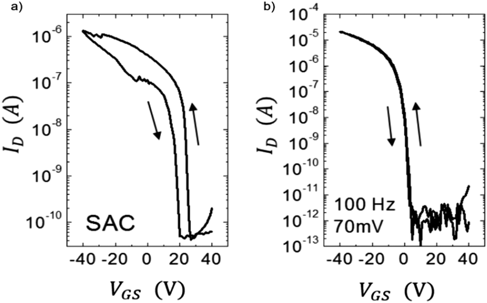 | ||
| Fig. 5 Hysteresis in IDvs. VGS curves for OFETs based on diF-TES ADT films processed from (a) SAC and (b) VAC. Adapted with permission from ref. 75, Copyright 2013, Wiley-VCH. | ||
5. Impact of traps on charge transport mechanisms
The temperature-dependence of charge carrier mobility provides insights into the mechanism of charge transport in a material. An increase in mobility upon cooling (i.e., μ ∝ T−n, 0 < n < 3) is typically observed in high quality OSC single crystals with low trap densities and was attributed to band-like transport.16,106,109,110,166–168 The presence of traps (density and distribution, both energetic and spatial) alter the charge transport mechanism significantly, and therefore the dependence of μ on T. As the trap densities increase, a transition from band-like to thermally-activated hopping regime can occur,126,169 where charge carriers assume band-like motion close to room temperature and are immobilized in the shallow trapping states at low temperatures, see for example the black curve in Fig. 6a obtained in rubrene single crystal OFETs.170 The temperature activated transport at low temperatures was modelled by an Arrhenius relation, , where Ea is the activation energy. The mobilities determined from Hall-effect measurements on the same crystal, however, increased with decreasing temperature in both the high and low temperature regimes (blue curve of Fig. 6a).170 Hall mobilities describe the motion of free charge carries, since trapped charges do not respond to the Lorentz force. Therefore, Hall measurements are indicative of intrinsic transport, where charge carriers move in delocalized bands in between trapping events. Fig. 6b shows μ vs. T plots for a solution processed 6,13,bis(triisopropylsilylethynyl) pentacene (TIPS-pentacene) OFET with Cytop dielectric obtained at different drain–source voltages.171 At low drain-voltages, the mobility exhibits an activated behavior over a wide temperature range, with a small activation energy of EA = 5.7 meV: in this regime the transport is dominated by shallow traps. At sufficiently high fields, the traps are filled, and as a result, μ increases with decreasing T. As mentioned in Section 3.2.1, the strain induced at the interface between the semiconductor and dielectric due to the CTE mismatch between consecutive device layers can also introduce traps. The example in Fig. 6c shows thermally-activated transport for the case of FETs fabricated at the interface between 2,8-difluoro-5,11-bis(triethylgermylethynyl) anthradithiophene (diF-TEG ADT) (CTE = 162 ppm K−1) and SiO2 dielectric (CTE = 4.1 ppm K−1) (blue circles).105 FETs fabricated on similar crystals, but with vacuum dielectric, where thermal strain is absent, exhibited band-like transport (black squares). Investigation of a large number of semiconductor/dielectric combinations confirmed that the result cannot be explained simply on the basis of Frölich polarons, and the microstrain plays a critical role. Laudari and Guha investigated charge transport in TIPS pentacene FETs with ferroelectric polymer dielectrics.172 While the reference FETs consisting of non-ferroelectric dielectric (SiO2) showed activated transport, a band-like temperature dependence of the mobility was observed within the ferroelectric temperature window in devices with poly(vinylidene fluoride-trifluoroethylene) (PVDF-TrFE) dielectric due to de-trapping of charge carriers from shallow traps arising from changes in the electric polarization of the dielectric. Merlo and Frisbie observed two distinct thermally-activated transport regimes in FETs based on RR P3HT nanofibers due to the presence of a double distribution of traps.125 The high activation energy in the high-temperature regime was attributed to the presence of deep donor-like traps, while the low-temperature regime exhibited a low activation energy resulting from acceptor-like shallow traps. A transition between the two regimes was observed, with the transition temperature depending on the gate voltage (195 K for VGS = −12 V and 250 K for VGS = −32 V). At larger gate voltages, since all deep traps are filled, the distinction between the two regions disappeared and only the effect of shallow traps was manifested in the Arrhenius plot. Nelson et al., observed both a temperature-independent mobility, and an activated charge transport in thin-film pentacene OFETs depending on the quality of the films (i.e. trap densities).173 A similar trend was found in solution deposited OSCs, where the activation energy was proportional to the trap densities.102
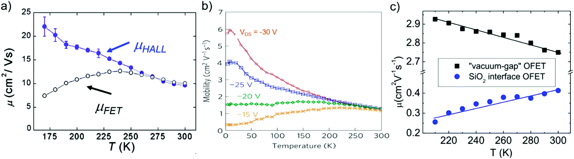 | ||
| Fig. 6 μ vs. T plots for (a) rubrene single crystals, adapted with permission from ref. 170, Copyright 2005, American Physical Society, (b) TIPS-pentacene thin films at different drain–source voltages, Adapted with permission from ref. 171, Copyright 2010, Springer Nature Ltd, and (c) diF-TEG ADT crystals with SiO2 dielectric (blue circles) and vacuum dielectric (black circles). Adapted from ref. 105, Copyright 2017, National Academy of Sciences. | ||
6. Experimental techniques to detect and characterize traps
Determining the origin, concentration and composition of charge carrier traps in OSCs, as well as their spatial and energetic distribution, is not trivial and remains a challenge, in spite of the tremendous efforts dedicated on this topic. Nevertheless, progress has been remarkable and access to the density of trap states spectra has led to significant improvements over the years in device performance and reliability. Several experimental techniques have been developed to access traps, but since each of them includes different levels of approximations, have varying sensitivities, and cover different ranges of energy distributions, the results are not always consistent. This section aims to cover the most popular experimental techniques employed in the detection and characterization of traps. The benefits and limitations of each technique, along with a few examples where they have been adopted will be outlined.6.1. Electrical measurements
 | (3) |
 | (4) |
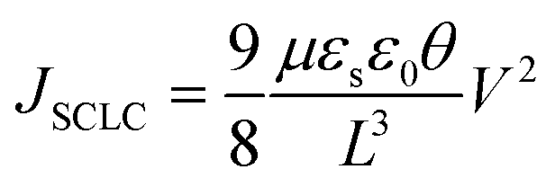
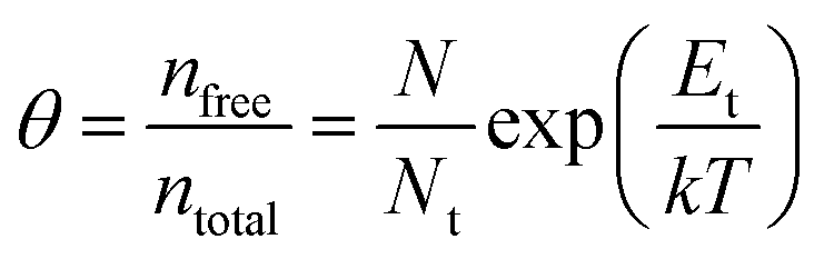
Fig. 7a illustrates a SCLC current–voltage curve for the case of a discrete shallow trapping state. The graph is characterized by the Ohmic region at low voltages, where the current increases linearly with voltage, then the SCLC regime at intermediate bias, followed by the SCLC trap-free regime at high voltages. The current in the latter two regimes follow a quadratic dependency on the applied voltage. The equations governing the current in each region are provided as inset.174 For a semiconductor with traps, a fraction of the injected charges will not participate in transport because they are captured by the traps. This results in a reduction in current by a factor of θ. Assuming one dominant trap state, at higher voltages, an abrupt transition from the space charge limited regime to the trap filled limit occurs when the quasi-Fermi level crosses the discrete trap level. This process is evident in the J–V curves as a sudden increase in the current at a voltage called the trap-filled limit voltage (VTFL) which is used to estimate Nt (per unit volume per unit energy):
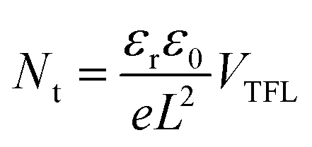 | (5) |
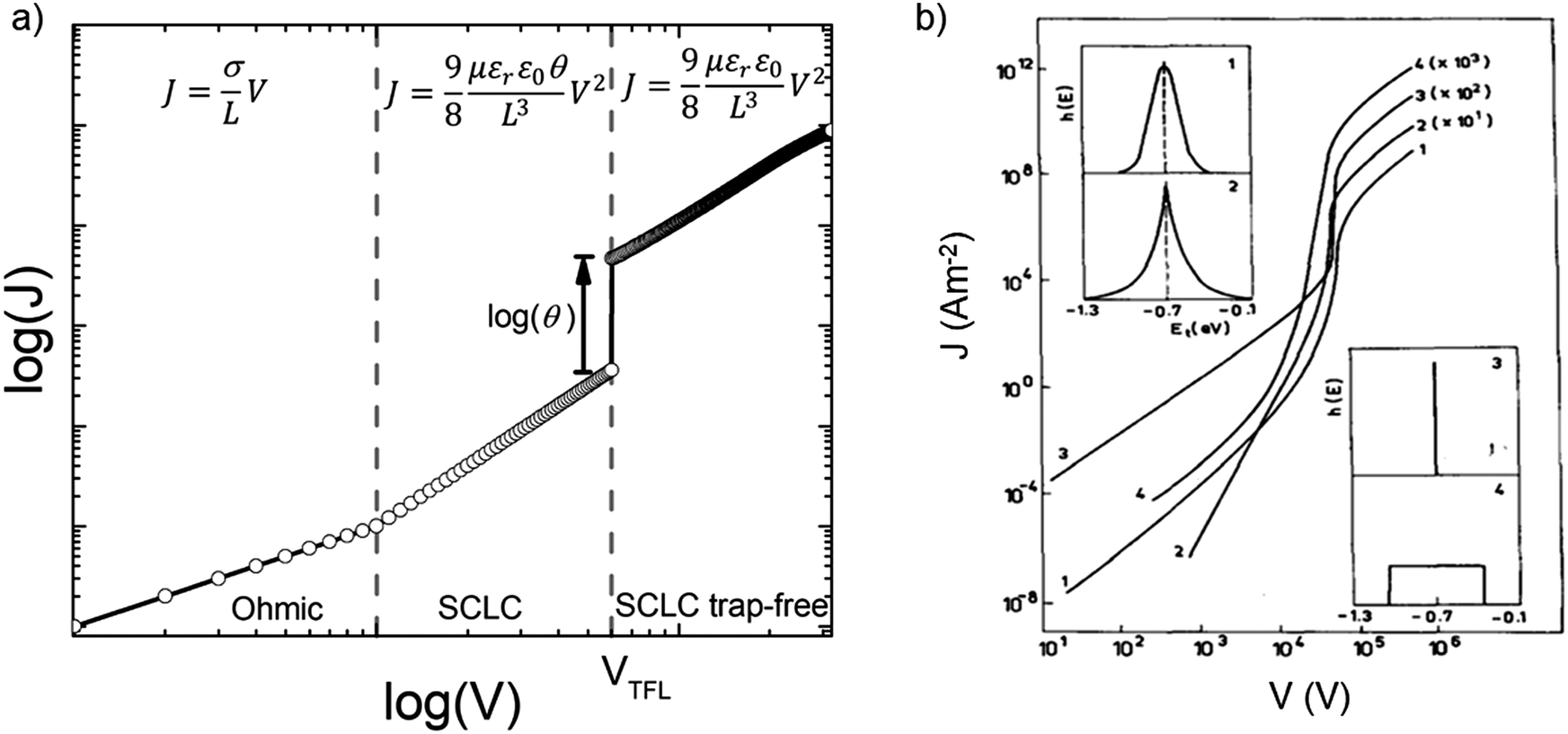 | ||
| Fig. 7 (a) Typical current–voltage characteristics from SCLC measurements for a discrete distribution of shallow traps characterized by the Ohmic, SCLC and SCLC trap-free regimes. Inset presents the equations governing J and V in the respective regimes. (b) Calculated current–voltage characteristics for various distributions of trapping states as shown in the insets (1) Gaussian distribution, (2) double exponential distribution, (3) discrete distribution and (4) uniform distribution, all centered at 0.7 eV from the valence band edge. Adapted with permission from ref. 182, Copyright 1990, Elsevier Ltd. | ||
For the case of multiple discrete trap states, the J–V curves exhibits several sharp increases in the current as the quasi-Fermi level crosses through each trap state. Reaching the trap-free limit is experimentally difficult, especially when the trap states are broadly distributed in energy, as it is the case in most OSCs. The oversimplified assumption of a single discrete distribution of shallow traps may be justified for ultra-pure single crystals, which are known to have very low density of traps, but it is not accurate for polycrystalline films. Further, the difficulty in interpreting the experimental J–V curves as they deviate from the J ∝ V2 dependency to other forms such as J ∝ Vn with n > 2 required that other types of distribution functions representing a quasi-continuous energy distribution of traps states be considered. A typical distribution is an exponential distribution of traps of the form:178
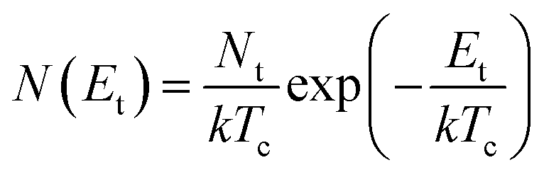 | (6) |
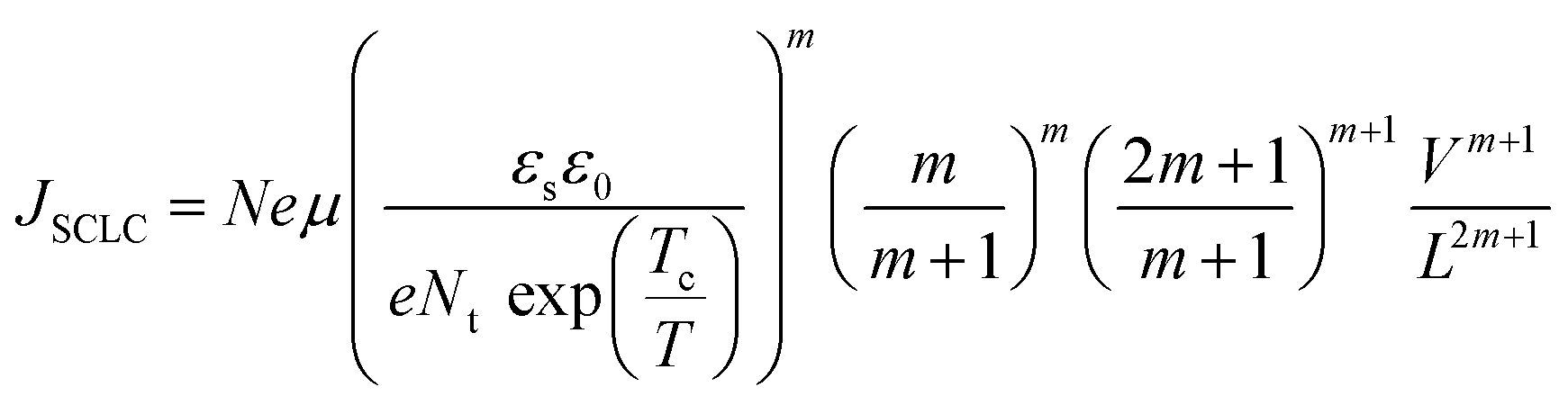 | (7) |
While an exponential distribution explains n > 2 exponent values, with n being a constant, it cannot resolve curves with n monotonously increasing with applied voltage.178,181 Other types of energy distributions have also been considered for the analysis of the J–V curves. The Gaussian distribution function proposed by Silinsh is an example.33 An S-shaped dependence observed in the logarithmic J–V plot at voltages above VTFL was attributed to Gaussian traps and in the case of several such distributions, a step-like J–V characteristics is evident.33 The analytical expression for J–V relation varies with the applied voltage range as the quasi-Fermi level coincides with different regions of the Gaussian (for example, tail or peak), depending on the voltage applied. Therefore, different analytical expressions have been proposed for different voltage ranges and slopes n.33Fig. 7b illustrates the J–V curves predicted for several trap distributions such as Gaussian, exponential and uniform. An important outcome of assuming quasi-continuous distributions is that it allows the determination of the trap DOS as a function of energy in the band gap. Such a deduction however requires modelling experimental J–V curves to expressions analytically or numerically derived from theoretical models which requires a priori assumptions on the energetic profile of traps. Since experimental curves are often interpreted using integrating techniques involving asymptotic equations, details of the energetic distributions can be lost, leading to incorrect results.182 Therefore, several efforts focused on developing methods for extraction of trap parameters from the experimental J–V curves for an arbitrary distribution of trap i.e., without making an a priori assumption on the energetic distribution. Nespurek and Sworakowski developed the differential method which took the first derivatives of the experimental J–V curves to extract trap parameters.183 Later, Schauer et al. put forward the thermally modulated SCLC method (TM-SCLC), also called temperature dependent SCLC (TD-SCLC), in which the energy of the trapping state is determined separately from the experimental activation energy, Ea of the conductivity σ, in addition to the differential evaluation of the J–V curves.183–185 The J–V curves are measured at different temperatures in order to determine Ea(V) from the slope of the Arrhenius plot ln![[thin space (1/6-em)]](https://www.rsc.org/images/entities/char_2009.gif) σ vs. 1/T. TD-SCLC measurements performed on high-purity single crystals of rubrene identified the presence of two exponential trap DOS: one with a steep distribution close to the band edge and another with a shallower distribution in the band gap.48 The breadth of the distribution, as well as the trap densities, varied from sample to sample due to the fact that the crystals are sensitive to growth conditions and atmospheric contaminants. The purest sample yielded deep trap densities as low as 1015 cm−3, while densities as high as 1017 cm−3 were measured in other crystals. In addition, traps created by means of a controlled exposure to activated oxygen were detected as a discrete peak in the DOS spectra at 0.27 eV above the mobility edge. More recently, Nikolka et al., characterized water-related traps in the bulk of polymer films using TD-SCLC.186 The addition of small molecular species displaced the water-induced traps to yield a narrow density of tail states (in the order of kT) near the band edge akin to that of molecular single crystals.
σ vs. 1/T. TD-SCLC measurements performed on high-purity single crystals of rubrene identified the presence of two exponential trap DOS: one with a steep distribution close to the band edge and another with a shallower distribution in the band gap.48 The breadth of the distribution, as well as the trap densities, varied from sample to sample due to the fact that the crystals are sensitive to growth conditions and atmospheric contaminants. The purest sample yielded deep trap densities as low as 1015 cm−3, while densities as high as 1017 cm−3 were measured in other crystals. In addition, traps created by means of a controlled exposure to activated oxygen were detected as a discrete peak in the DOS spectra at 0.27 eV above the mobility edge. More recently, Nikolka et al., characterized water-related traps in the bulk of polymer films using TD-SCLC.186 The addition of small molecular species displaced the water-induced traps to yield a narrow density of tail states (in the order of kT) near the band edge akin to that of molecular single crystals.
Effects such as diffusion currents, non-homogeneity of the sample, spatial distribution of traps and the existence of an energy barrier at the metal/semiconductor interface are neglected in SCLC theory. This poses difficulties in accurately interpreting the experimental J–V curves and several new models have been proposed to refine SCLC analysis.183–185,187–192 The effect of the diffusion component on the current has been introduced by Bonham.187,188 Dacuña and Salleo included contact asymmetry and diffusion currents to characterize the trap distribution.190 They assumed a mobility edge model with a Gaussian distribution of traps centered around 0.2 eV to obtain numerical solutions to the drift–diffusion equation, but the model could only reproduce data within the energy range of 0.1–0.3 eV. Diffusion currents caused by contact asymmetry masked the states shallower than 0.1 eV and deeper than 0.3 eV and a work function offset of 0.58 eV for both contacts was necessary to match the experimental data. Khan and Xun later extended this model to include a DOS with an exponential tail in addition to the Gaussion.191 Dacuña and Salleo also showed that the assumption of a homogeneous trap distribution is invalid and that an asymmetric distribution of traps exists in the semiconductor.193 A spatial distribution of traps near the top contact (with a trap density of 1.2 × 1012 cm−3 and a characteristic width of 32.3 nm from the semiconductor/metal interface) was needed to model the experimental curves of a rubrene crystal under both forward and reverse conditions over different temperatures.
While SCLC measurements are experimentally easy to perform as they only require two-terminal current–voltage measurements, careful analysis, often involving advanced numerical modelling, is required for the accurate determination of trap parameters. For this reason, OFET measurements take preference in the extraction of trap DOS spectrum. In addition, as the charge carrier density, and hence the qausi-Fermi level, is modulated by the gate voltage independently of the current in the transistor channel, OFET measurements are more versatile in the extraction of trap parameters as will be discussed in the following section.
The simplest methods for extracting information about traps using OFETs involve the threshold voltage Vth and subthreshold swing S. Details on the determination of Vth, and S and are provided in a recent tutorial focused on OFETs.10 Since Vth is the gate–source voltage required to fill traps at the organic/semiconductor interface before mobile charge carriers are accumulated in the transistor channel, it can be used to estimate the concentration of traps that are filled per unit area, Nsit,
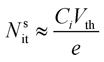 | (8) |
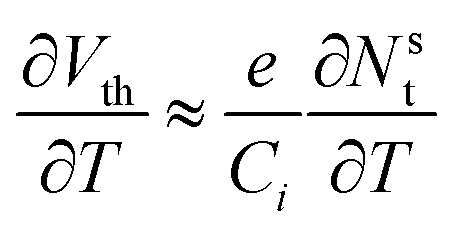 | (9) |
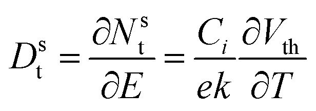 | (10) |
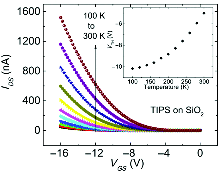 | ||
| Fig. 8 Transfer characteristics of a TIPS pentacene OFET with SiO2 dielectric measured at different temperatures. Inset shows the threshold voltage as a function of temperature. Reproduced with permission from ref. 172 Copyright 2016, American Physical Society. | ||
Eqn (10) was used to determine the areal trap density close to the HOMO band edge in rubrene single crystals with an air-gap dielectric.126Vth increased quasi-linearly upon cooling and a density of 1012 cm−2 eV−1 was evaluated from the slope of the Vthvs. T plot.
Another method to evaluate the trap density is by measuring S. The following expression for the subthreshold swing can be used to estimate the density of interfacial trap states.194
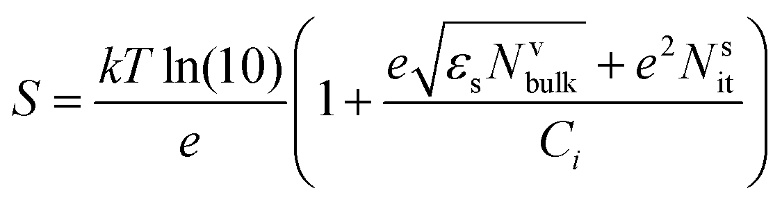 | (11) |
Podzorov and coworkers used photo-induced charge carriers in the channel of a single crystal tetracene OFET with parylene dielectric to extract information about shallow traps.195 Application of a gate bias under illumination (VillumGS) caused charge carriers to move across the dielectric/OSC interface and into the dielectric, resulting in a shift in the turn-on voltage, Von. A monotonic decrease in mobility was observed when electrons were transferred, and no change was detected upon transfer of holes due to the fact that electrons immobilized in the dielectric create potential wells that act as shallow traps while the holes create potential bumps that only scatter them. The density of photo-induced charges was estimated from the shift in Von using ΔN = CiΔVon/e. By measuring the mobility as a function of the photo-induced density of shallow traps, μ(N), a trap density of (3 ± 0.5) × 1011 cm−2 (prior to illumination) and an average trapping lifetime of 50 ± 10 ps was evaluated.
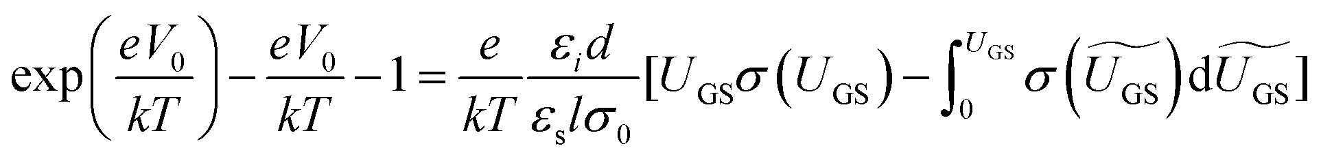
The above methods provide a useful comparison of shallow and deep trap densities, but they do not provide details on the energy distribution of the trapping states within the bad gap, i.e., the trap DOS function. In order to quantitatively determine the trap DOS, several analytical methods and numerical methods have been developed. In the following, a few methods will be discussed to varying extents. Determination of the trap DOS spectrum exploits the fact that the gate bias induces band bending at the interface between the semiconductor and the dielectric. Fig. 9 depicts the energy diagram for gate/dielectric/semiconductor interface in three voltage regimes. A p-channel transistor is considered here and the extension to n-channel transistors can be obtained by changing the sign of the gate voltage and considering states in the upper half of the band gap. An initial band bending occurs even under zero bias due to energy level mismatch between the adjacent layers (Fig. 9a). In order to achieve flat bands, a gate–source voltage called the flat band voltage (VFB) in necessary (Fig. 9b). Increasing the voltage beyond VFB causes band bending, as illustrated in Fig. 9c, and an arbitrary trap state with energy E (represented by red solid lines) is now elevated at the interface to coincide with the quasi-Fermi level. E corresponds to the shift in the energy bands relative to the quasi-Fermi-level at the interface (x = 0), i.e., E = EV − EF − eV0, where EV and EF are the energy of the valence band edge and the Fermi energy respectively, and V(x = 0) = V0 is the interface potential. The dependence of V0 on VGS, i.e. the function V0 (VGS), is the key to obtaining the DOS spectrum and several models have been developed to extract DOS from this function. The method by Grunewald et al., developed for a-Si transistors and later adopted for OFETs by Kalb et al.,196,197 is based on the gate voltage dependence of the field-effect conductivity. The model assumes that the semiconductor layer is homogeneous and accounts for the initial band bending by calculating the gate–source voltage above the flat band voltage, i.e., UGS = |VGS − VFB|.196VFB is assumed to be the turn-on voltage estimated from the transfer curve. The function V0 (VGS) is then obtained by numerically solving the following equation (see ref. 196 for a complete derivation):
 | (12) |
 | (13) |
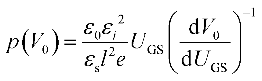 | (14) |
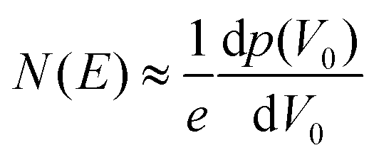 | (15) |
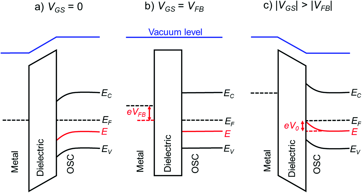 | ||
| Fig. 9 Energy level diagram at the gate/dielectric/semiconductor interface of an OFET at different gate bias, (a) at VGS = 0 showing initial band bending at the dielectric/semiconductor interface, (b) at VGS = VFB illustrating flat bands and (c) at |VGS| > |VFB| depicting gate-induced band bending. Solid red lines represent an arbitrary trap state for holes, solid black lines the band edges and the broken black lines the Fermi level of the respective material. | ||
Grünewald's method has been widely explored by the scientific community to determine the trap DOS spectrum. Diemer et al. compared the trap DOS at two different semiconductor/dielectric interfaces, namely the interface of diF-TES ADT thin films with the fluorinated polymer dielectric Cytop and the SiO2 dielectric.97 Devices with Cytop dielectric yielded two orders of magnitude lower trap densities (see Fig. 10a), which resulted in an order of magnitude higher charge carrier mobilities compared to the devices with SiO2 dielectric (an average of 0.17 ± 0.19 cm2 V−1 s−1 and 1.5 ± 0.70 cm2 V−1 s−1 for SiO2 and Cytop, respectively). Paterson et al. investigated the impact of charge carrier trapping at the semiconductor/dielectric interface on contact resistance by comparing small-molecule/polymer-blend OFETs with two polymer dielectrics, Cytop and AF2400.98 The trap DOS spectrum, evaluated as a function of energy from the qausi Fermi level, indicated similar trap densities deep in the band gap, but increasing much more rapidly for devices with AF2400 as the energy approached the band edge. Devices with AF2400 yielded lower total trap densities and lower contact resistance. In the same study, the DOS analysis was performed on bias-stressed devices and was found that no trapping/detrapping occurs during operation of AF2400 devices. Grünewald's method has also been employed to investigate the effect of p-doping an OSC blend containing the small molecule 2,7-dioctyl [1]benzothieno[3,2-b][1]benzothiophene (C8-BTBT) and the co-polymer IDT-BT (see Fig. 10b).198 A shift in trap DOS was observed only for dopant concentrations higher than 1 mol%, with pinning of the quasi-Fermi level dominating at lower dopant concentration.
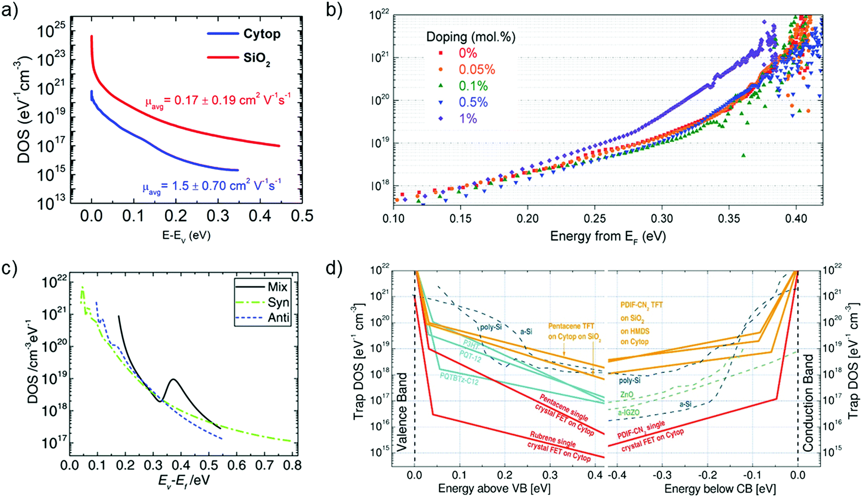 | ||
| Fig. 10 (a) Comparison of the interfacial trap DOS spectrum for diF-TES ADT films with Cytop (blue) and SiO2 (red) dielectrics evaluated using Grünewald's model. The value of mobility is listed in the inset. Adapted with permission from ref. 97, Copyright 2015, AIP Publishing LLC. (b) Effect of p-doping on the trap DOS of OSC/polymer blend OFETs evaluated using Grünewald's model. Reproduced with permission from ref. 198, Copyright 2017, Wiley-VCH. (c) Effect of isomer purity of diF-TES ADT on the trap DOS spectrum determined using Method II by Kalb et al. Broken green and blue curves represent trap DOS of pure syn- and anti-isomers respectively while the solid black lines represent that of the mix sample for reference. Reproduced with permission from ref. 205, Copyright 2017, Wiley-VCH. (d) Comparison of the interfacial trap DOS for several organic and inorganic FETs calculated using the numerical method by Oberhoff et al. Reproduced with permission from ref. 208, Copyright 2010, American Physical Society. | ||
Grunewald's method considers only the potential drop at the dielectric layer caused by the gate–source voltage and does not account for the potential drop across the interface. i.e., VGS − VFB = Vdielectric. Such an assumption is justified for devices with thick dielectrics operating at high voltages. In the case of devices operating at low-voltage and with thin dielectrics, however, the potential drop across the semiconductor can be comparable to that across the dielectric and hence cannot be ignored. Recently Geiger et al. addressed this issue and extended the Grünewald's method for low-voltage devices by accounting for the potential drop at the interface, i.e., VGS − VFB = Vdielectric + V0.199 The model was used to calculate the DOS spectrum of two different thin film transistors consisting of a thick and a thin gate dielectric. Devices with thick dielectric yielded similar results using both the original and extended methods. However, a significant difference in trap DOS was observed for devices with thin dielectric, with the newly proposed method being more accurate.
Several other analytical methods such as those by Horowitz et al.,200 Lang et al.,201 Fortunato et al.,202 and Kalb et al.,203,204 exist to extract the trap DOS spectrum. These methods are based on the temperature dependence of the field-effect conductivity and therefore require temperature dependent measurements. These methods rely on the concept of the quasi-Fermi level shift induced by a change in the gate–source voltage that, in turn, corresponds to a shift in the activation energy of the conductivity. The activation energy Ea of the field-effect conductivity is evaluated as a function of gate–source voltage, i.e., Ea (VGS), in order to determine the energy E of the trapping state (E ≈ Ea = EV − EF − eV0). The field-effect conductivity is related to the temperature by an Arrhenius relation and therefore by measuring the transfer characteristics at different temperatures, the activation energy at each gate–source voltage can be determined with a linear regression analysis of lnσ vs. 1/T. Several approximations differentiate the methods. For example, Lang et al. consider the charge accumulation thickness ‘a’ to be independent of the gate–source voltage,201 while Horowitz et al. include the gate voltage dependency in their calculations.200 Fortunato et al. calculate the activation energy of the first derivative of the normalized field-effect conductivity.202 Kalb et al. proposed two methods with method II an extension of method I, which follows eqn (14) and (15), but with the interface potential evaluated from the activation energy of the conductivity. Method II by Kalb et al. was formulated following Fortunato et al., who considered a normalized field-effect conductivity in order to account for the temperature dependence of the band mobility μ0.202,204 This method revealed a discrete trapping state in the band gap of in diF-TES ADT originating from the co-existence of anti and syn isomers, as illustrated in Fig. 10c.205 Ha et al. calculated the trap DOS spectrum for both holes and electrons in an ambipolar transistor based on diketopyrrolopyrrole–benzothiadiazole (PDPP–TBT) copolymer using the method by Lang et al. and method II by Kalb et al.206 Both methods yielded similar results with symmetric trap distributions for both holes and electrons.
The analytic methods discussed so far approximate the Fermi-function to that at zero temperature and neglect the temperature dependence of the Femi energy EF and interface potential V0. The numerical method developed by Oberhoff et al. incorporates Fermi–Dirac statistics into the calculations for the determination of the trap DOS function.207 In this method, a computer program simulates the linear regime transfer characteristics at any temperature for a given distribution of traps and band mobility μ0. The parameters describing the DOS are varied until the generated transfer characteristics are a good fit to the experimentally measured curves. A constant DOS at the band edges, with exponential tail states decaying into the band gap, is assumed. The program allows the introduction of an additional Gaussian distribution to account for any discrete trap states. Fig. 10d compares the trap DOS spectrum of several p-channel and n-channel OFETs, as well as some inorganic FETs, calculated using the numerical model by Oberhoff et al.208 This plot reveals similar trap DOS in OSCs and inorganic semiconductor thin films despite significant differences in charge carrier mobility. Single crystal FETs occupy the lowest part of the graph, with trap densities several orders of magnitude lower than their thin film counterparts. This highlights the effect of both disorder and morphology on the trap DOS spectrum. In a recent study, Anand et al. found that for devices with similar film morphologies, the nature of the dielectric is the main factor that determines the overall trap densities.102
Fig. 11 compares the trap DOS spectrum calculated using all the methods described in this section applied for the same device, a pentacene thin-film transistor.204 It is clear that both the choice of the method and the parameters assumed a priori impact the final results.204 The trap density estimated from the subthreshold swing using eqn (11) is independent of energy and provides only a rough estimate for traps in the vicinity of the quasi-Fermi level located in the mid gap (∼0.5 eV from EV). To be noted that the curve obtained from the simulation program accounts for complete Fermi–Dirac statistics and therefore the accuracy of all other curves are evaluated with respect to this. The method by Lang et al. underestimates the trap densities, as evident from the slope of the curve near the band edge, which was attributed to the fact that the dependence of the accumulation layer thickness on the gate-voltage was neglected. Method II by Kalb et al. and Fortunato et al. have better agreement with the results from simulation as they allow for the temperature dependence of band mobility.
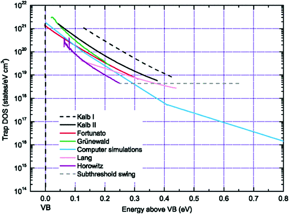 | ||
| Fig. 11 A comparison of the interfacial trap DOS obtained for pentacene thin-film transistors using several analytical and numerical methods. Adapted with permission from ref. 204, Copyright 2010, American Physical Society. | ||
Takeya and coworkers developed a new technique to extract the trap DOS spectrum by employing McWhorter's model for the measured flicker noise (1/f noise).209 The noise arising from current fluctuations hamper OFET stability and can originate from different sources, with contact effects and charge carrier trapping being the most common.58 In this study, the authors assumed that charge trapping is the main noise source and evaluated the trap DOS spectrum from the spectral density in the current noise. The results agree well with those from the numerical model by Oberhoff discussed earlier. By drastically reducing the structural disorder, they obtained charge carrier mobilities as high as 15 cm2 V−1 s−1, band-like transport and record low flicker noise.
C–V measurements at different frequencies provide estimates for the trap densities, but cannot determine the energy distributions, for which equivalent circuit and C–f modelling is needed. Equivalent circuit modelling has been employed to determine trap distributions in organic metal–insulator–semiconductor (MIS) capacitors based on (P3HT) and various polymer-based gate insulators.212,213 Although it is a simple technique that allows for fast analysis of the impedance spectra, the challenge lies in determining an appropriate model that correlates with the frequency response of real devices. C–f eliminates the above problem and hence is more often used to characterize traps. During C–f modelling, the frequency of the applied voltage is swept until a characteristic frequency at which charges are thermally excited out of trap states is recorded. This frequency is used to determine the trapping timescale (i.e. ω = 2πf). Walter et al. proposed a model for CuIn(Ga)2Se solar cells, which was later adopted for OPVs, in order to extract the trap distribution using the following equation:217
 | (16) |
6.2. Optical and thermal methods
Optical and thermal methods are based on the photo-induced (radiative) and thermally induced (non-radiative) transitions among electronic states, respectively. The presence of charge carrier trapping states in the band gap will inevitably impact such measurements, and this can be exploited in determining the nature and energetic distribution of traps.One optical method is photoemission spectroscopy (PES), also known as photoelectron spectroscopy (PS), which is based on the principle of photoelectric effect. The energy of the emitted electrons is measured in order to determine their binding energy. The ionization energy needed for photoelectric effect is provided by various sources such as X-ray (XPS) or UV (UPS) photons. This method has been used to observe directly the band gap states of single crystals of rubrene and C60.225,226 UPS measurements have been employed to detect Au-induced112 and disorder/defect-induced227 band gap states in thin polycrystalline films of pentacene. In C60, a higher density of states was detected near the valence band edge (1019–1021 eV−1 cm−3) which originated from exposure to atmospheric gases with a negligible contribution from structural defects such as grain boundaries.225
Light absorbed by the semiconductor excites the charge carriers residing in the trap states into the conduction states, thereby generating free charge carriers and subsequently increasing the electrical conductivity of the sample, a phenomenon called photoconductivity. Thus by measuring the changes in the current caused by changes in the conductivity, information on the distribution of traps can be obtained. This method has been used for example, to extract the interfacial trap DOS spectrum in thin film pentacene-based transistors.228
Charge modulation spectroscopy, which probes changes in the optical absorption of the OSC caused by the loss/acquisition of electrons from molecular orbitals, is another powerful spectroscopic technique that has been used in characterizing traps. When combined with temperature-dependent electrical measurements, such as FET or two-point measurements in a diode configuration, CMS can provide insights into trapping mechanisms.47,171 The applied voltage modulates the charge carrier concentration during which shallow trap sates are filled and emptied, subsequently causing changes in the absorption (CMS) spectrum. Sakanoue et al. observed a sharpening of the absorption peak in the CMS spectra of TIPS-pentacene OFETs at low temperature (150–200 K) and correlated it to the temperature dependence of mobility.171 The sharpening was observed in the temperature regime where mobility was thermally activated and hence was attributed to shallow traps. The absorption peak broadened as the lateral electric field (drain–source voltage) was increased, implying that charges residing in shallow trap states can be de-trapped into mobile states by application of the drain–source voltage. Charge modulation spectroscopy has also been used to observe dynamic disorder induced tail states in various solution-processed small molecules.47
Optical methods are useful to characterize shallow traps, but cannot resolve deep non-radiative traps, where methods that also require thermal excitations are adopted. One such technique is the thermally-stimulated current (TSC) measurement, which involves the filling of band gap states using charges from injection or light absorption followed by thermal excitation of the trapped charges. The filling of traps is typically done at low temperature (∼70 K) to ensure they are not released immediately.32 The sample is then gradually heated until the trapped charges gain enough thermal energy to get excited out of the trap states, subsequently increasing the current. The current is recorded as function of temperature to obtain trap density and depth. The resolution of this technique depends on the rate of sample heating. Trapping states with depths of 0.03–0.06 eV and 0.13–0.18 eV have been identified using the TSC spectra of OLEDs based on the polymer poly(p-phenylenevinylene) (PPV).229 The shallow trap was eliminated by replacing the ITO electrode with Au, depicting that the reaction of ITO with products eliminated during conversion of the PPV precursor (such as HCl) lead to the formation of the trap. The deep trap, on the other hand, appeared regardless of the electrode material and was attributed to interaction with the environment. Tsang et al. investigated the effect of introducing interlayers of 8-hydroxyquinolinato lithium between the hole blocking and electron transporting layers in OLEDs based on a green emitter (4s,6s)-2,4,5,6-tetra(9H-carbazol-9-yl) isophthalonitrile (4CzIPN).230 The measurements indicated the reduction in the deep charge carrier trap density upon insertion of the interlayer that subsequently enhanced the operational stability of the devices.
Deep level transient spectroscopy (DLTS) is another useful technique for the characterization of traps. The standard technique, originally developed for inorganic materials, is based on measuring the transient capacitance of a device during a thermal scan as a function of time upon applying a voltage pulse.231 When the voltage pulse is turned on, the quasi-Fermi level moves in the band gap filling up trap states as it crosses them and when turned-off, the trapped charges are thermally excited into the bands. Hence, variations in the transient capacitance due to the discharge of excited charge carriers provide information on trap parameters. However, since OSCs generally have longer relaxation times compared to conventional semiconductors, only small variations in capacitance are evident, making it challenging to accurately extract trap parameters. A modified DLTS technique based on the measurement of charges released from trapping centers instead of variations in capacitance, hence called charge-based DLTS (Q-DLTS), yielded better accuracy.232 In addition, this technique distinguishes between majority and minority carrier traps. This method has been used to obtain the density, depth and capture cross section in OLEDs based on PPV,232,233 its derivatives,234 and 4,4′-bis(4-dimethylaminostryryl) (DMASB).233 Electronic trap distributions in OPV materials PCBM, P3HT and blends of PCBM/P3HT have been obtained using this method.235 Trap activation energies of 87 meV and 21 meV were evaluated for pure P3HT and PCBM, respectively. The blends yielded activation energies ranging from 30–160 meV due to differences in the rate of emission of charge carriers from the trap states.
Photothermal deflection spectroscopy (PDS) is based on the photothermal deflection of a laser beam while measuring changes in the thermal properties of a material upon absorption of light. In this technique, the sample is immersed in a fluid of refractive index that is sensitive to changes in temperature. A monochromatic beam of light is shone on the sample to excite the charge carriers into the gap states. The excited charges then decay non-radiatively, emitting heat in the process, which subsequently changes the temperature of the liquid immersed in. A probe laser beam grazing the surface of the substrate deflects upon detecting this photo-thermally induced change. The measurement is repeated at each wavelength of the incident beam.236 PDS spans from near-IR to the UV spectral range (∼0.1–4 eV).32 Higher sensitivities can be achieved by increasing the light exposure time at each wavelength, but this can result in long measurement times.32Fig. 12a show the PDS spectra obtained for rubrene single crystals.32 The trap DOS was characterized using three exponential functions (indicated as offset broken lines) with a steep slope of ∼36 meV close to band edge and increasing to ∼61 meV at intermediate energies and finally to ∼170 meV deep in the band gap. In addition, a broadening of the DOS was observed for X-ray irradiated crystals (open circles) in comparison to the pristine crystals (open squares). The high sensitivity of this method lead to detection of molecular vibrational modes in the PDS spectrum, as indicated by arrows in Fig. 12a. However, this can be problematic as the absorption from vibrations could mask the features obtained from electronic transitions.32 PDS has also been used to probe band gap tail states in conjugated polymers resulting from energetic disorder.79,186 Besides, the width of the density of the tail states have been estimated in terms of the Urbach energy. Urbach energy of several high-mobility conjugated polymers with varying crystallinity has been determined and correlated with the extent of energetic disorder.79Fig. 12b shows the PDS spectra for four polymers, namely IDT-BT (black), poly(2,5-bis(3-alkylthiophen-2-yl)thieno(3,2-b)thiophene) PBTTT (red) and diketopyrrolopyrrole (DPP) based polymers, DPPTTT (green), PSeDPPBT (blue).79 Exponential tail fits (solid lines) are included to determine Urbach energies, which are indicated in the inset. IDT-BT yielded the sharpest absorption onset translating into the lowest Urbach energy of 24 meV, a value which is less than kT at room temperature, in agreement with its excellent performance in OFETs.78
 | ||
| Fig. 12 (a) PDS spectrum of as-prepared (open squares) and X-ray exposed (open circles) rubrene single crystal. Broken lines represent exponential fits for different spectral regions and are offset for clarity. Arrows represent absorption peaks resulting from molecular vibrations. Reproduced with permission from ref. 32, Copyright 2013 Wiley-VCH. (b) PDS spectra of several high-mobility polymers. Solid lines represent exponential fits to determine the Urbach energy of each polymer indicated in the inset. Reproduced with permission from ref. 79, Copyright 2014, Springer Nature Ltd. | ||
6.3. Scanning probe methods
Scanning probe techniques such as electric force microscopy (EFM) and Kelvin probe force microscopy (KPFM) provide high spatial resolution imaging and map the topography of a surface by detecting changes in the local contact potential.237 Trapped charge carriers modify the local contact potential and hence these techniques provide an excellent tool to determine the origin of traps as well as their spatial distribution. Both KPFM and EFM have been widely used to investigate the role of grain boundaries on charge carrier trapping in organic thin films.64,65,67 Recently, KPFM was used to identify crystal step edges as sources of traps for electrons in single crystals of n-type semiconductor Cl2-NDI.55 KPFM performed on a rubrene derivative revealed planar defects resulting from a solid–solid phase transition during cooling.238 Such defects cause electronic disorder that could potentially introduce charge carrier traps. Mathijssen et al. studied the dynamics of trap formation in OFETs upon exposure to ambient conditions. They found that bias-stress effects were caused by water-related traps originating at the SiO2 dielectric surface rather than in the OSC.133 Dougherty and coworkers used KPFM images to map the fluctuations in surface potential in the transistor channel of an ultrathin α-sexithiophene (α-6T) OFET arising from trapping and de-trapping of charge carrier from shallow traps.239 They showed that the spatial distribution of these fluctuations is uniform throughout the active channel.Various other techniques can be useful in the detection of traps. For example, micro Raman imaging has been adopted to detect the coexistence of isomers in diF-TES ADT films,240 which has been previously reported to create a discrete trap state in the same material.205 X-ray based techniques such as wide angle X-ray scattering (WAXS), small angle X-ray scattering (SAXS) and resonant soft X-ray scattering and reflectivity (r-SoXS/R) have been used to identify structural defects, grain boundaries, interface roughness in several OSCs which also serve as potential charge carrier traps.241 Evidence for electrochemical trapping of electrons by silanol groups in the SiO2 dielectric has been acquired using multiple-reflection attenuated-total-reflection Fourier transformed infrared (ATR-FTIR) spectrometry.96
7. Exploitation of charge carrier traps for organic sensing devices
While traps are typically regarded as an obstacle to achieving high performance in organic electronic devices, they can also be exploited towards sensing any factors that can modulate the trap DOS spectra, e.g. impurities (chemical and biological), temperature, light, or radiation. The generation or passivation of charge carrier traps in OFETs causes a measurable change in the device performance and hence imparts the sensing mechanism. These changes may be harnessed to detect chemical, biological or physical agents. Sensors based on OFETs have several advantages, including biocompatibility, ease of processing, and versatility in molecular design to address the sensitivity and selectivity challenges well beyond the capabilities of sensors made from inorganic materials.242–246 This section will provide a review of chemical, thermal and radiation sensors as well as memory devices that take advantage of charge trapping/de-trapping to perform sensing operations.7.1. Chemical sensors
The sensitivity of OSCs to environmental molecules, i.e. ‘analytes’, make them excellent candidates for gas sensing and odor analysis. These analytes can interact with an OSC through hydrogen bonding and π interactions, or through reversible and irreversible chemical reactions.247 These interactions may occur within the bulk of the material, at grain boundaries, or at device interfaces (metal/semiconductor, or semiconductor/dielectric).248 Chemical sensing with OFETs can be quite complicated, as there are diverse mechanisms by which the OSC interacts with chemicals. This section will focus on sensing mechanisms which depend on trap formation, but there can be other, non-trap related effects that have been exploited for sensing with OFETs. For an in-depth description of chemical sensing with OFETs, we refer the reader to several thorough reviews on the subject.242,243,249,250Using OFETs as the active element in chemical sensors allows for a greater range of response than equivalent two-terminal devices, since chemical changes can affect the mobility, threshold voltage, or the on/off current ratio.251 One method of sensing relies on the interaction of polar analytes with the OSC. When the OFET is exposed to a polar analyte, the dipolar molecules induce local variations in the electric fields in the OSC. Depending on the energy levels of the analyte with respect to the OSC, trap states can be introduced causing mobile charges to be localized on the analyte, resulting in a lowering of the drain current or a shift in the threshold voltage.242 These effects are mediated by the processes occurring at the grain boundaries, where the disorder leads to an increased polarizability of charge carriers. The density of grain boundaries is related to the sensitivity of devices to analytes; polar analytes trap charges at the grain boundaries, localizing charges in tail states, resulting in a lower overall current, and the response is greater upon increasing the polarity of molecules.252,253 The seemingly unlimited choices of OSCs offer excellent tunability to different analytes,253,254 and could be integrated into electronic noses,255 which can be used to detect, analyze, and identify odors in many applications. Assuming that each analyte interacts with a given OSC in a distinct way, its presence and concentration may be identified by measuring the change in operation of the device, allowing circuits composed of multiple different OSCs to detect specific analytes. These devices could be implemented in analyzing food freshness by sensing propanol and acetic acid,255 in identifying traces of explosives256 and nerve gas,257 and detecting hazardous chemicals in work environments, at parts per million level, or below.258,259
Depending on the nature of the analyte, changes to the OSC film can be reversible or irreversible: highly reactive gases, such as NO2, cause irreversible changes to films though chemisorption, but this can be healed via a high temperature annealing step, as shown in a copper phthalocyanine device.247 Ammonia gas (NH3) is an example of a polar analyte which can be reversibly sensed using OFETs, since it desorbs from the surface once the gas is removed from the environment. Ammonia sensing is also in high demand as it is a highly toxic and corrosive agent, and due to its ubiquitous use in industrial and agricultural settings. Katz and coworkers demonstrated an OFET based on poly(3,3′′′-didodecylquaterthiophene) (PQT-12) with a sensitivity of 0.5 ppm when exposed to ammonia, and more recently showed that this effect is exhibited in both n-type and p-type OSCs, 2,20-[(2,5-dihexadecyl-3,6-dioxo-2,3,5,6-tetrahydropyrrolo-[3,4-c]pyrrole-1,4-diylidene)dithiene-5,2-diyli-dene]dimalononitrile (DPPCN) and P3HT, respectively.260,261 In addition to a high sensitivity, these devices exhibited a high selectivity to ammonia, and a memory effect when cooled. Adsorption of ammonia onto the surface of the semiconductor induced energetic disorder and charge–dipole interactions, which resulted in a decrease in the drain current of the device. By a similar route, adsorption of ammonia onto spray-coated TIPS pentacene caused a threshold voltage shift, and a decrease in mobility and drain current.248 Ethanol was detected using pentacene OFETs by studying the temperature dependence of mobility; the authors showed that exposure to ethanol vapors increases the activation energy, indicating that charges are deeply trapped when the vapor is introduced.262
7.2. Temperature sensors
The development of small, light-weight, and biocompatible temperature sensors has the potential to revolutionize the medical field. Temperature and pressure sensing has been achieved through the use of OFETs coupled with capacitive elements, such as a microstructured PDMS,263 or by using piezoelectrics as sensing elements, in series with the gate of an OFET.264,265 More recently, temperature sensing relying on trapping allowed for the entire sensor to be contained within a single OFET device, without additional hardware or processing, offering a clear advantage over the more complicated and bulky capacitance-based devices.As discussed in Section 5, the temperature dependence of mobility is strongly related to the density and distribution (both energetic and spatial) of traps. Strategic choices of dielectric materials can be used to impart a greater range of thermal sensitivity and expand the sensor use. For example, OFETs based on dielectrics with strong polar groups, such as polyactide (PLA), have a high trap density (both deep and shallow) at the semiconductor/dielectric interface.245 By adding heat into the system, carriers are released from traps, and the threshold voltage showed a sensitivity of ∼0.25 V K−1, with a nearly linear response, making this a viable method to creating temperature sensors. In addition to imparting temperature sensitivity beyond room temperature, PLA is biocompatible, making it an appealing material for use in medical applications. This strategy has also been employed using other polar dielectrics, such as poly-(vinyl alcohol) with a copper phthalocyanine (CuPc) semiconductor, which exhibited a similar temperature response above room temperature, with reversible changes in device operation.266 More recent work has shown that different metal atoms can impart metal phthalocyanines with an increased response to temperature, such as Mg and Fe, without the use of a polar dielectric layer, which could lead to simpler fabrication techniques than dielectric modification.267
7.3. Light/radiation sensors
Photodetectors and radiation detectors based on OSCs are very appealing; their biocompatibility and conformability make them useful in applications ranging from medical research, such as sensors attached to the skin,246,268 to industrial applications.269 This section will focus on near-infrared (NIR), visible light, ultra-violet (UV), and high-energy radiation sensors which rely on charge trapping.When incident photons are absorbed into the OSC, an exciton is created, which then diffuses through the OSC until it reaches a trap (e.g. defect, impurity, or surface state) where it dissociates into a free electron and a hole. Holes and electrons may encounter donor or acceptor-like traps, respectively, causing an increase in the current density in the channel as well as a shift in the threshold voltage.270 The sensing mechanism relies on trapping and de-trapping of the majority or minority carriers, which reduces the recombination rate, thus enhancing the concentration of one carrier type. The trap sensitivity can be manipulated by choice of the dielectric, or by utilizing semiconductor blends which strategically increase the trap density.269,271
Sensing in the near infrared has many potential applications in imaging, night vision, health diagnosis, and industrial monitoring. One example is a bulk heterojunction of poly(N-alkyl diketopyrrolo-pyrrole dithienylthieno[3,2-b]thiophene)(DPP-DTT) and PCBM in a phototransistor configuration. The narrow bandgap and high absorption in the near-infrared make these materials ideal for NIR sensing. The devices exhibited responsivities of up to 5 × 10⁵ A W−1, with a gain of ∼104, though the responsivity decreases with light intensity due to filling of longest-lived trap states, leaving the short-lived trap states to dominate the gain effects.272 A similar strategy was used by Sun et al., who added PbS quantum dots in P3HT thin-film transistors. In this case the electrons were trapped on the PbS domains, and responsivities up to 2 × 10⁴ A W−1 were achieved; for reference neat P3HT showed negligible photoresponse.273 Qiu, et al. used bis(2-oxoindolin-3-ylidene)-benzodifuran-dione (PBIBDF-TT) nanowires (PBIBDF-TT absorbs in the NIR region) to fabricate photodetectors, and recorded the highest sensitivity when SiO2 was used as dielectric owing to the high trap density characteristic to these devices.269 Operation in air increased the photoresponse further, and the authors postulated that the high surface/volume ratio increased the number of trap sites from adsorbed H2O and O2, which further traps photogenerated charges, increasing the photoconductive gain.
Efforts focused on visible light sensing rely primarily on charge trapping at the dielectric surface.271 Park et al. fabricated pentacene FET devices using poly(methyl methacrylate) (PMMA), poly(4-vinylphenol) (PVP), and Cytop dielectrics, and studied the impact of the dielectric on photosensitivity: PMMA contains an ester group, which acts as a trapping site for holes, PVP has electron trapping hydroxyl groups, and Cytop is inert. They found that the FETs with PVP dielectric showed the greatest photo response and the traps induced a hysteresis effect, which is useful in memory applications. By increasing the concentration of hydroxyl groups in the PVP layer, the authors were able to increase the photocurrent and hysteresis effect. While PMMA and Cytop did not give the hysteresis effect, they still exhibited a mild photoresponse, which was attributed to trapping at the grain boundaries in the pentacene film. A similar effect was observed by Kim et al., in inkjet printed α,ω-dihexylquarterthiophene (DH4T) OFETs with a PVP dielectric: they found that electron trapping shifts the threshold voltage and results in an increase in the density of photoinduced holes in the channel.274 Polyactide (PLA) dielectrics also increase photosensitivity by introducing strong polar groups into the dielectric. This dielectric allowed them to detect light with intensity as low as 0.02 mW cm−2, with a photosensitivity of 104.275
The detection of UV light often requires the use of filters or waveguides to separate UV from visible light,276 which increases the complexity of traditional UV sensors. Smithson et al. demonstrated a sensor which was inert to visible light, and only detected UV radiation, without the need for complicated waveguides.277 This was achieved by creating a blend of a polymer binder with strong electron donating amine groups, azobenzene derivative disperse red 1 (p-DR1), and 2,7-dipentyl[1]benzothieno[3,2-b][1]benzothiophene (C5-BTBT) and recording the shift in the threshold voltage as a function of the intensity of the radiation. Huang et al. used an electret layer, namely a doped triphenylamine (TPA)-based polymer, between the pentacene film and the dielectric layer, to achieve UV sensing and an UV programmable memory effect. The electret layer serves a dual function: first, upon UV irradiation, it has an emission peak which overlaps the absorption peak of pentacene, enhancing exciton creation, and second, it traps electrons from dissociated excitons, increasing the hole photocurrent. The trapped electrons may be ‘erased’ with UV light, serving the memory function, though the responsivity of these devices was low, at ∼45 A W−1.278
Sensing of ionizing radiation (X-rays/γ-rays), as well as the sensing of charged particles, such as protons, is a subject of recent attention,279,280 owing to the possible applications that they may enable. While in some devices the sensing mechanism is similar to that used to detect NIR and visible light, other devices rely on the creation of traps in devices when exposed to radiation. Batlogg and coworkers showed that proton irradiation of single crystal rubrene created deep trap states in the crystal, which was attributed to a breaking in the C–H bonds.141 They also showed that X-ray irradiation causes local disorder in the crystal, a common source of traps in OSCs.281 Proton irradiation of TIPS pentacene OFETs resulted in a decrease in device mobility as a result of the fact that the heavy particles caused structural disorder within the organic film.282 In the same material, it has been shown that irradiation with X-rays produces a photoconductive gain effect: the authors attributed this to an increase in the conductivity of the films by the accumulation of free charge carriers, which act as a dopant.280 Later, they amplified the photoconductive gain by using a FET configuration and substituting TIPS-pentacene with diF-TES ADT and diF-TEG ADT. The inclusion of Si and Ge atoms into the molecular structure provided a high-Z component, which increased the response to high energy photons because of the high scattering cross section of these atoms.279
7.4. Memory devices based on charge trapping
A robust control of the dynamics of charge trapping led to its exploitation in memory applications; long-lived trap states induce shifts in current–voltage characteristics, and while such behavior is not desired for a typical device operation (see for example the effects described in Section 4), it can give rise to discrete memory states. The memory states form the basis for a variety of applications, from imparting memory capabilities to flexible circuits to mimicking neurons in neuromorphic circuits for artificial intelligence and deep learning.283–287 In synaptic memory devices, control of the charge trapping was accomplished by doping the OSC with either non-metallic particles (e.g. ZnO),288 or metallic particles (e.g. Au).289 These particles trap charges in the conduction channel, therefore altering the device characteristics. Memories based on this method have long retention times, but need to be ‘read’ by applying a gate voltage, which can affect the stored memory state.284 Techniques which make use of photochromic molecules, such as spiropyran, azobenzene, or diarylethene, can overcome this limitation, since the memory is switched by light, and not the electric field.290 These molecules change their conformation upon exposure to UV light, which is key to their function as memory devices.291,292 For example, Samorì and coworkers utilized a blend of diarylethene (DAE) photochromic molecules P3HT to realize a photo-switchable memory device.293 When the DAE was exposed to UV light, the isomer ‘switched’ to the closed state, whose HOMO was within the bandgap of the P3HT, and therefore acted as a hole trap, reducing the current of the device. The trapping/de-trapping was highly stable and reversible: DAE molecules revert to the open isomer by exposure to visible light, and the devices modulated the current continuously, allowing many possible memory states, imparting organic electronic devices the ability to act as memory devices in complex circuits.8. Summary and future perspectives
Charge carrier trapping is ubiquitous in OSCs and is a direct consequence of van der Waals intermolecular interactions inherent in these materials. The details on the nature, spatial and energetic distribution of traps, as well as timescales of trapping/de-trapping events, have a profound impact on the performance of organic electronic devices. Studies related to the subject date back to the 1960s, when the research focused almost exclusively on free standing molecular crystals.33,34,54 Later, the effort was expanded to address charge carrier trapping occurring in thin films and at device interfaces. Tail states introduced by dynamic disorder arising from thermal motions and their role in charge carrier trapping have also recently garnered attention. In this review, we aimed to provide readers with a comprehensive overview on the phenomenon of charge carrier trapping in OSC materials and opto-electronic devices. Beginning with the definition of traps, we then discussed their origin and properties, categorized the sources of traps in OSCs and provided examples for each case. Sources of traps range from structural defects to chemical impurities, from devices interfaces to environmental effects, with many of these effects being coupled. A discussion on the impact of charge carrier trapping on the mechanism of charge transport and the performance of organic electronic devices was provided, including strategies adopted to mitigate these effects for optimal device function. Next, we discussed the experimental techniques available for the detection and characterization of traps. Optical and thermal methods rely on radiative and non-radiative electronic transitions between localized band gap states enabling the extraction of trap parameters, with thermal methods having the potential of probing deeper band gap states. Electrical measurements in device configurations such as OFETs and two terminal devices serve as excellent tools to extract energetic distribution of traps, while scanning probe techniques are useful in determining the spatial distribution of traps. Applications such as chemical, temperature and radiation sensors, in which the phenomenon of charge carrier trapping is exploited for detection were briefly discussed.Remarkable progress has been made over the years in terms of characterization of traps, clarifying the impact on charge transport and reducing undesirable effects through innovations in material design and device fabrication. Increasingly better understanding of the phenomenon has led to new design rules for organic devices, and made the reduction in the density of charge carrier traps possible. For example, OSCs with an ionization energy of less than 6 eV and an electron affinity greater than 3.6 eV are predicted to yield trap-free charge transport of both holes and electrons, which is an important milestone achieved that can subsequently enhance device performance to a great extent.86 Despite the numerous efforts, unanswered questions still persist. Most methods for trap characterization are indirect and require different levels of approximations, often making the interpretation of results difficult. Systematic studies involving deliberate incorporation of traps to investigate their effect on the DOS spectrum are rare. Access to each source of trap independently would clarify its impact on charge transport, but this is practically impossible because many trapping events are correlated (e.g. an impurity generates energetic as well as structural disorder). In addition, studying the dynamics of trap states is another challenging direction of future research. Elucidating the time evolution of trap states will aid in comprehending the effect of dynamic disorder, the major performance-limiting factor in electronic devices. Resolving these issues, coupled with progress in understanding and enhancing charge injection, development of new materials, and optimizing device structure, will lead to significant improvements in the performance of electronic devices, enabling their full potential to be realized in real-world applications.
Conflicts of interest
The authors declare no conflicts of interest.Acknowledgements
This work was supported by the National Science Foundation through Grant No. DMR-1627925 and ECCS-1810273.References
- A. C. Arias, J. D. MacKenzie, I. McCulloch, J. Rivnay and A. Salleo, Chem. Rev., 2010, 110, 3–24 CrossRef CAS PubMed
.
- N. Gasparini, A. Salleo, I. McCulloch and D. Baran, Nat. Rev. Mater., 2019, 4, 229–242 Search PubMed
- H. Sirringhaus, Adv. Mater., 2014, 26, 1319–1335 CrossRef CAS PubMed
- H. Klauk, Chem. Soc. Rev., 2010, 39, 2643 RSC
- J. E. Anthony, A. Facchetti, M. Heeney, S. R. Marder and X. Zhan, Adv. Mater., 2010, 22, 3876–3892 CrossRef CAS
- M. Kuik, G. J. A. H. Wetzelaer, H. T. Nicolai, N. I. Craciun, D. M. De Leeuw and P. W. M. Blom, Adv. Mater., 2014, 26, 512–531 CrossRef CAS
- J. L. Bredas, J. P. Calbert, D. A. da Silva Filho and J. Cornil, Proc. Natl. Acad. Sci. U. S. A., 2002, 99, 5804–5809 CrossRef CAS PubMed
- V. Coropceanu, J. Cornil, D. A. da Silva Filho, Y. Olivier, R. Silbey and J.-L. Brédas, Chem. Rev., 2007, 107, 926–952 CrossRef CAS PubMed
- A. Troisi and G. Orlandi, J. Phys. Chem. A, 2006, 110, 4065–4070 CrossRef CAS PubMed
- Z. A. Lamport, H. F. Haneef, S. Anand, M. Waldrip and O. D. Jurchescu, J. Appl. Phys., 2018, 124, 071101 CrossRef
- J.-P. Yang, F. Bussolotti, S. Kera and N. Ueno, J. Phys. D: Appl. Phys., 2017, 50, 423002 CrossRef
- C. D. Dimitrakopoulos and P. R. L. Malenfant, Adv. Mater., 2002, 14, 99–117 CrossRef CAS
- S. Fratini, D. Mayou and S. Ciuchi, Adv. Funct. Mater., 2016, 26, 2292–2315 CrossRef CAS
-
E. A. Silinsh and V. Capek, Organic Molecular Crystals: Interacton Localization, and Transport Phenomena, AIP Press, New York, 1994 Search PubMed
- A. Troisi, Chem. Soc. Rev., 2011, 40, 2347–2358 RSC
- N. A. Minder, S. Ono, Z. Chen, A. Facchetti and A. F. Morpurgo, Adv. Mater., 2012, 24, 503–508 CrossRef CAS PubMed
- S. Ciuchi, S. Fratini and D. Mayou, Phys. Rev. B: Condens. Matter Mater. Phys., 2011, 83, 081202 CrossRef
-
S. M. Sze and K. K. Ng, Physics of Semiconductor Devices, Wiley-Interscience, Hoboken, NJ, 2007 Search PubMed
- G. Horowitz, J. Appl. Phys., 2015, 118, 115502 CrossRef
- A. R. Völkel, R. A. Street and D. Knipp, Phys. Rev. B: Condens. Matter Mater. Phys., 2002, 66, 195336 CrossRef
- J. Rivnay, R. Noriega, J. E. Northrup, R. J. Kline, M. F. Toney and A. Salleo, Phys. Rev. B: Condens. Matter Mater. Phys., 2011, 83, 121306 CrossRef
- N. Mott, J. Phys. C: Solid State Phys., 1987, 20, 3075–3102 CrossRef CAS
- H. Bässler, Phys. Status Solidi, 1993, 175, 15–56 CrossRef
- I. V. Arkhipov, P. Heremans, E. V. Emelianova, G. J. Adriaenssens and H. Bässler, J. Phys.: Condens. Matter, 2002, 14, 9899–9911 CrossRef
- J. P. Sleigh, D. P. McMahon and A. Troisi, Appl. Phys. A: Mater. Sci. Process., 2009, 95, 147–152 CrossRef CAS
- K. Willa, R. Häusermann, T. Mathis, A. Facchetti, Z. Chen and B. Batlogg, J. Appl. Phys., 2013, 113, 133707 CrossRef
- J. E. Anthony, C. Warwick, L. Jiang, M. Nikolka, Y. Henri Geerts, H. Sirringhaus, G. Schweicher, A. S. Eggeman, A. Troisi, S. G. Yeates and S. Illig, Nat. Commun., 2016, 7, 10736 CrossRef
- O. Simonetti and L. Giraudet, Polym. Int., 2019, 68, 620–636 CrossRef CAS
- G. Horowitz and P. Delannoy, J. Appl. Phys., 1991, 70, 469–475 CrossRef CAS
- G. Horowitz, P. Lang, M. Mottaghi and H. Aubin, Adv. Funct. Mater., 2004, 14, 1069–1074 CrossRef CAS
- M. C. J. M. Vissenberg and M. Matters, Phys. Rev. B: Condens. Matter Mater. Phys., 1998, 57, 12964–12967 CrossRef CAS
-
A. Salleo, Organic Electronics, Wiley-VCH Verlag GmbH & Co. KGaA, Weinheim, Germany, 2013, pp. 341–380 Search PubMed
-
E. A. Silinsh, Organic Molecular Crystals: Their electronic states, Springer Berlin Heidelberg, Berlin, Heidelberg, 1980 Search PubMed
- E. A. Silinsh, Phys. Status Solidi, 1970, 3, 817–828 CrossRef
- A. Rose, Phys. Rev., 1955, 97, 1538–1544 CrossRef CAS
- J. Sworakowski and K. Pigoń, J. Phys. Chem. Solids, 1969, 30, 491–496 CrossRef CAS
- S. D. Baranovskii, Phys. Status Solidi B, 2014, 251, 487–525 CrossRef CAS
- P. W. Anderson, Phys. Rev., 1958, 109, 1492–1505 CrossRef CAS
- T. F. Harrelson, V. Dantanarayana, X. Xie, C. Koshnick, D. Nai, R. Fair, S. A. Nuñez, A. K. Thomas, T. L. Murrey, M. A. Hickner, J. K. Grey, J. E. Anthony, E. D. Gomez, A. Troisi, R. Faller and A. J. Moulé, Mater. Horiz., 2019, 6, 182–191 RSC
- H. T. Yi, Y. N. Gartstein and V. Podzorov, Sci. Rep., 2016, 6, 23650 CrossRef CAS PubMed
- A. V. Nenashev, J. O. Oelerich and S. D. Baranovskii, J. Phys.: Condens. Matter, 2015, 27, 093201 CrossRef CAS PubMed
- S. D. Baranovskii, Phys. Status Solidi A, 2018, 215, 1700676 CrossRef
- N. R. Tummala, Z. Zheng, S. G. Aziz, V. Coropceanu and J.-L. Brédas, J. Phys. Chem. Lett., 2015, 6, 3657–3662 CrossRef CAS PubMed
- A. Troisi and G. Orlandi, Phys. Rev. Lett., 2006, 96, 086601 CrossRef PubMed
- D. L. Cheung and A. Troisi, Phys. Chem. Chem. Phys., 2008, 10, 5941–5952 RSC
- S. Ciuchi and S. Fratini, Phys. Rev. B: Condens. Matter Mater. Phys., 2012, 86, 245201 CrossRef
- A. Y. B. Meneau, Y. Olivier, T. Backlund, M. James, D. W. Breiby, J. W. Andreasen and H. Sirringhaus, Adv. Funct. Mater., 2016, 26, 2326–2333 CrossRef CAS
- C. Krellner, S. Haas, C. Goldmann, K. P. Pernstich, D. J. Gundlach and B. Batlogg, Phys. Rev. B: Condens. Matter Mater. Phys., 2007, 75, 245115 CrossRef
- S. Haas, A. F. Stassen, G. Schuck, K. P. Pernstich, D. J. Gundlach, B. Batlogg, U. Berens and H. J. Kirner, Phys. Rev. B: Condens. Matter Mater. Phys., 2007, 76, 115203 CrossRef
- H. Jiang and W. Hu, Angew. Chem., Int. Ed., 2019, 2–23 Search PubMed
- P. M. Robinson and H. G. Scott, Phys. Status Solidi, 1967, 20, 461–471 CrossRef CAS
- J. M. Thomas and J. O. Williams, Prog. Solid State Chem., 1971, 6, 119–154 CrossRef CAS
- F. Lohmann and W. Mehl, J. Chem. Phys., 1969, 50, 500–506 CrossRef CAS
-
M. Pope and C. E. Swenberg, Electronic Processes in Organic Crystals and Polymers, Oxford University Press, 1999 Search PubMed
- T. He, Y. Wu, G. D’Avino, E. Schmidt, M. Stolte, J. Cornil, D. Beljonne, P. P. Ruden, F. Würthner and C. D. Frisbie, Nat. Commun., 2018, 9, 2141 CrossRef PubMed
- S. S. Lee, C. S. Kim, E. D. Gomez, B. Purushothaman, M. F. Toney, C. Wang, A. Hexemer, J. E. Anthony and Y.-L. Loo, Adv. Mater., 2009, 21, 3605–3609 CrossRef CAS
- H. H. Choi, A. F. Paterson, M. A. Fusella, J. Panidi, O. Solomeshch, N. Tessler, M. Heeney, K. Cho, T. D. Anthopoulos, B. P. Rand and V. Podzorov, Adv. Funct. Mater., 2019, 1903617 CrossRef
- O. D. Jurchescu, B. H. Hamadani, H. D. Xiong, S. K. Park, S. Subramanian, N. M. Zimmerman, J. E. Anthony, T. N. Jackson and D. J. Gundlach, Appl. Phys. Lett., 2008, 92, 132103 CrossRef
- J. Rivnay, L. H. Jimison, J. E. Northrup, M. F. Toney, R. Noriega, S. Lu, T. J. Marks, A. Facchetti and A. Salleo, Nat. Mater., 2009, 8, 952–958 CrossRef CAS
- R. Li, J. W. Ward, D.-M. Smilgies, M. M. Payne, J. E. Anthony, O. D. Jurchescu and A. Amassian, Adv. Mater., 2012, 24, 5553–5558 CrossRef CAS PubMed
- C. P. L. Rubinger, H. F. Haneef, C. Hewitt, D. Carroll, J. E. Anthony and O. D. Jurchescu, Org. Electron., 2019, 68, 205–211 CrossRef CAS
- S. Hunter and T. D. Anthopoulos, Adv. Mater., 2013, 25, 4320–4326 CrossRef CAS
- L. G. Kaake, P. F. Barbara and X.-Y. Zhu, J. Phys. Chem. Lett., 2010, 1, 628–635 CrossRef CAS
- E. M. Muller and J. A. Marohn, Adv. Mater., 2005, 17, 1410–1414 CrossRef CAS
- M. Jaquith, E. M. Muller and J. A. Marohn, J. Phys. Chem. B, 2007, 111, 7711–7714 CrossRef CAS PubMed
- M. J. Jaquith, J. E. Anthony and J. A. Marohn, J. Mater. Chem., 2009, 19, 6116–6123 RSC
- K. Puntambekar, J. Dong, G. Haugstad and C. D. Frisbie, Adv. Funct. Mater., 2006, 16, 879–884 CrossRef CAS
- G. Horowitz, M. E. Hajlaoui and R. Hajlaoui, J. Appl. Phys., 2000, 87, 4456–4463 CrossRef CAS
- M. Tello, M. Chiesa, C. M. Duffy and H. Sirringhaus, Adv. Funct. Mater., 2008, 18, 3907–3913 CrossRef CAS
- L. C. Teague, B. H. Hamadani, O. D. Jurchescu, S. Subramanian, J. E. Anthony, T. N. Jackson, C. A. Richter, D. J. Gundlach and J. G. Kushmerick, Adv. Mater., 2008, 20, 4513–4516 CrossRef CAS
- T. W. Kelley and C. D. Frisbie, J. Phys. Chem. B, 2001, 105, 4538–4540 CrossRef CAS
- S. S. Lee, J. M. Mativetsky, M. A. Loth, J. E. Anthony and Y. L. Loo, ACS Nano, 2012, 6, 9879–9886 CrossRef CAS PubMed
- L. H. Jimison, M. F. Toney, I. McCulloch, M. Heeney and A. Salleo, Adv. Mater., 2009, 21, 1568–1572 CrossRef CAS
- J. H. Kang, D. Da Silva Filho, J. L. Bredas and X. Y. Zhu, Appl. Phys. Lett., 2005, 86, 152115 CrossRef
- P. J. Diemer, C. R. Lyle, Y. Mei, C. Sutton, M. M. Payne, J. E. Anthony, V. Coropceanu, J. Brédas and O. D. Jurchescu, Adv. Mater., 2013, 25, 6956–6962 CrossRef CAS
- D. Abbaszadeh, A. Kunz, N. B. Kotadiya, A. Mondal, D. Andrienko, J. J. Michels, G.-J. A. H. Wetzelaer and P. W. M. Blom, Chem. Mater., 2019, 31, 6380–6386 CrossRef CAS
- W. Graupner, G. Leditzky, G. Leising and U. Scherf, Phys. Rev. B: Condens. Matter Mater. Phys., 1996, 54, 7610–7613 CrossRef CAS PubMed
- Z. A. Lamport, K. J. Barth, H. Lee, E. Gann, S. Engmann, H. Chen, M. Guthold, I. McCulloch, J. E. Anthony, L. J. Richter, D. M. DeLongchamp and O. D. Jurchescu, Nat. Commun., 2018, 9, 5130 CrossRef
- D. Venkateshvaran, M. Nikolka, A. Sadhanala, V. Lemaur, M. Zelazny, M. Kepa, M. Hurhangee, A. J. Kronemeijer, V. Pecunia, I. Nasrallah, I. Romanov, K. Broch, I. McCulloch, D. Emin, Y. Olivier, J. Cornil, D. Beljonne and H. Sirringhaus, Nature, 2014, 515, 384–388 CrossRef CAS PubMed
- A. Karki, G. A. H. Wetzelaer, G. N. M. Reddy, V. Nádaždy, M. Seifrid, F. Schauer, G. C. Bazan, B. F. Chmelka, P. W. M. Blom and T. Nguyen, Adv. Funct. Mater., 2019, 29, 1901109 CrossRef
-
N. Karl, in Organic semiconductors, ed. H. J. Queisser, Festkörperprobleme, Springer Berlin Heidelberg, 1974, pp. 261–290 Search PubMed
- N. Karl, K.-H. Kraft, J. Marktanner, M. Münch, F. Schatz, R. Stehle and H.-M. Uhde, J. Vac. Sci. Technol., A, 1999, 17, 2318–2328 CrossRef CAS
- K. H. Probst and N. Karl, Phys. Status Solidi, 1975, 27, 499–508 CrossRef CAS
- O. D. Jurchescu, J. Baas and T. T. M. Palstra, Appl. Phys. Lett., 2004, 84, 3061–3063 CrossRef CAS
- P. K. Nayak, R. Rosenberg, L. Barnea-Nehoshtan and D. Cahen, Org. Electron., 2013, 14, 966–972 CrossRef CAS
- N. B. Kotadiya, A. Mondal, P. W. M. Blom, D. Andrienko and G. A. H. Wetzelaer, Nat. Mater., 2019, 18, 1182–1186 CrossRef CAS PubMed
- G. Zuo, M. Linares, T. Upreti and M. Kemerink, Nat. Mater., 2019, 18, 588–593 CrossRef CAS PubMed
- G. Zuo, Z. Li, O. Andersson, H. Abdalla, E. Wang and M. Kemerink, J. Phys. Chem. C, 2017, 121, 7767–7775 CrossRef CAS
- S. Olthof, S. Mehraeen, S. K. Mohapatra, S. Barlow, V. Coropceanu, J.-L. Brédas, S. R. Marder and A. Kahn, Phys. Rev. Lett., 2012, 109, 176601 CrossRef PubMed
- M. L. Tietze, J. Benduhn, P. Pahner, B. Nell, M. Schwarze, H. Kleemann, M. Krammer, K. Zojer, K. Vandewal and K. Leo, Nat. Commun., 2018, 9, 1182 CrossRef PubMed
- M. L. Tietze, P. Pahner, K. Schmidt, K. Leo and B. Lüssem, Adv. Funct. Mater., 2015, 25, 2701–2707 CrossRef CAS
- B. Lüssem, M. Riede and K. Leo, Phys. status solidi, 2013, 210, 9–43 CrossRef
- H. Sirringhaus, Adv. Mater., 2005, 17, 2411–2425 CrossRef CAS
- R. R. Dasari, X. Wang, R. A. Wiscons, H. F. Haneef, A. Ashokan, Y. Zhang, M. S. Fonari, S. Barlow, V. Coropceanu, T. V. Timofeeva, O. D. Jurchescu, J. Brédas, A. J. Matzger and S. R. Marder, Adv. Funct. Mater., 2019, 1904858 CrossRef CAS
- L. L. Chua, P. K. H. Ho, H. Sirringhaus and R. H. Friend, Adv. Mater., 2004, 16, 1609–1615 CrossRef CAS
- L. Chua, J. Zaumseil, J. Chang, E. C.-W. Ou, P. K.-H. Ho, H. Sirringhaus and R. H. Friend, Nature, 2005, 434, 194–199 CrossRef CAS
- P. J. Diemer, Z. A. Lamport, Y. Mei, J. W. Ward, K. P. Goetz, W. Li, M. M. Payne, M. Guthold, J. E. Anthony and O. D. Jurchescu, Appl. Phys. Lett., 2015, 107, 103303 CrossRef
- A. F. Paterson, A. D. Mottram, H. Faber, M. R. Niazi, Z. Fei, M. Heeney and T. D. Anthopoulos, Adv. Electron. Mater., 2019, 5, 1800723 CrossRef
- Y.-Y. Noh, X. Cheng, A. Facchetti, H. Yan, H. Sirringhaus, J. Wang, M. Caironi and C. Newman, Chem. Mater., 2010, 22, 1559–1566 CrossRef
- W. L. Kalb, T. Mathis, S. Haas, A. F. Stassen and B. Batlogg, Appl. Phys. Lett., 2007, 90, 2005–2008 CrossRef
- D. Knipp, P. Kumar, A. R. Völkel and R. A. Street, Synth. Met., 2005, 155, 485–489 CrossRef CAS
- S. Anand, K. P. Goetz, Z. A. Lamport, A. M. Zeidell and O. D. Jurchescu, Appl. Phys. Lett., 2019, 115, 073301 CrossRef
- M. Abe, T. Mori, I. Osaka, K. Sugimoto and K. Takimiya, Chem. Mater., 2015, 27, 5049–5057 CrossRef CAS
- M. J. Kang, I. Doi, H. Mori, E. Miyazaki, K. Takimiya, M. Ikeda and H. Kuwabara, Adv. Mater., 2011, 23, 1222–1225 CrossRef CAS PubMed
- Y. Mei, P. J. Diemer, M. R. Niazi, R. K. Hallani, K. Jarolimek, C. S. Day, C. Risko, J. E. Anthony, A. Amassian and O. D. Jurchescu, Proc. Natl. Acad. Sci. U. S. A., 2017, 114, E6739–E6748 CrossRef CAS PubMed
- I. N. Hulea, S. Fratini, H. Xie, C. L. Mulder, N. N. Iossad, G. Rastelli, S. Ciuchi and A. F. Morpurgo, Nat. Mater., 2006, 5, 982–986 CrossRef CAS PubMed
- A. F. Stassen, R. W. I. De Boer, N. N. Losad and A. F. Morpurgo, Appl. Phys. Lett., 2004, 85, 3899–3901 CrossRef CAS
- J. Veres, S. D. Ogier, S. W. Leeming, D. C. Cupertino and S. M. Khaffaf, Adv. Funct. Mater., 2003, 13, 199–204 CrossRef CAS
- V. C. Sundar, Science, 2004, 303, 1644–1646 CrossRef CAS PubMed
- E. Menard, V. Podzorov, S.-H. Hur, A. Gaur, M. E. Gershenson and J. A. Rogers, Adv. Mater., 2004, 16, 2097–2101 CrossRef CAS
- Y. Wu, A. R. Chew, G. A. Rojas, G. Sini, G. Haugstad, A. Belianinov, S. V. Kalinin, H. Li, C. Risko, J. L. Brédas, A. Salleo and C. D. Frisbie, Nat. Commun., 2016, 7, 10270 CrossRef CAS PubMed
- T. Sawabe, K. Okamura, T. Sueyoshi, T. Miyamoto, K. Kudo, N. Ueno and M. Nakamura, Appl. Phys. A: Mater. Sci. Process., 2009, 95, 225–232 CrossRef CAS
- M. Oehzelt, N. Koch and G. Heimel, Nat. Commun., 2014, 5, 4174 CrossRef CAS
- C. Liu, Y. Xu and Y. Y. Noh, Mater. Today, 2015, 18, 79–96 CrossRef CAS
- J. C. Scott, J. Vac. Sci. Technol., A, 2003, 21, 521–531 CrossRef CAS
- M. Waldrip, O. D. Jurchescu, D. J. Gundlach and E. G. Bittle, Adv. Funct. Mater., 2019 DOI:10.1002/adfm.201904576
- D. Natali and M. Caironi, Adv. Mater., 2012, 24, 1357–1387 CrossRef CAS
- H. Baessler and G. Vaubel, Phys. Rev. Lett., 1968, 21, 615–617 CrossRef CAS
- R. W. I. de Boer and A. F. Morpurgo, Phys. Rev. B: Condens. Matter Mater. Phys., 2005, 72, 073207 CrossRef
- M. Coll, K. P. Goetz, B. R. Conrad, C. A. Hacker, D. J. Gundlach, C. A. Richter and O. D. Jurchescu, Appl. Phys. Lett., 2011, 98, 163302 CrossRef
- K. Kuribara, H. Wang, N. Uchiyama, K. Fukuda, T. Yokota, U. Zschieschang, C. Jaye, D. Fischer, H. Klauk, T. Yamamoto, K. Takimiya, M. Ikeda, H. Kuwabara, T. Sekitani, Y. L. Loo and T. Someya, Nat. Commun., 2012, 3, 723–727 CrossRef
- C.-Y. Wang, C. Fuentes-Hernandez, J.-C. Liu, A. Dindar, S. Choi, J. P. Youngblood, R. J. Moon and B. Kippelen, ACS Appl. Mater. Interfaces, 2015, 7, 4804–4808 CrossRef CAS
- X. Jia, C. Fuentes-Hernandez, C.-Y. Wang, Y. Park and B. Kippelen, Sci. Adv., 2018, 4, eaao1705 CrossRef
- M. Nikolka, I. Nasrallah, B. Rose, M. K. Ravva, K. Broch, A. Sadhanala, D. Harkin, J. Charmet, M. Hurhangee, A. Brown, S. Illig, P. Too, J. Jongman, I. McCulloch, J. Bredas and H. Sirringhaus, Nat. Mater., 2017, 16, 356–362 CrossRef CAS
- J. A. Merlo and C. D. Frisbie, J. Phys. Chem. B, 2004, 108, 19169–19179 CrossRef CAS
- V. Podzorov, E. Menard, A. Borissov, V. Kiryukhin, J. A. Rogers and M. E. Gershenson, Phys. Rev. Lett., 2004, 93, 086602 CrossRef CAS PubMed
- C. Pannemann, T. Diekmann and U. Hilleringmann, J. Mater. Res., 2004, 19, 1999–2002 CrossRef CAS
- T. Komoda, K. Kita, K. Kyuno and A. Toriumi, Jpn. J. Appl. Phys., Part 1, 2003, 42, 3662–3665 CrossRef CAS
- Y. W. Wang, H. L. Cheng, Y. K. Wang, T. H. Hu, J. C. Ho, C. C. Lee, T. F. Lei and C. F. Yeh, Thin Solid Films, 2004, 467, 215–219 CrossRef CAS
- Z.-T. Zhu, J. T. Mason, R. Dieckmann and G. G. Malliaras, Appl. Phys. Lett., 2002, 81, 4643–4645 CrossRef CAS
-
I. Kymissis, Organic Field Effect Transistors, Springer US, Boston, MA, 2009 Search PubMed
- L. Tsetseris and S. T. Pantelides, Phys. Rev. B: Condens. Matter Mater. Phys., 2007, 75, 153202 CrossRef
- S. G. J. Mathijssen, M. Kemerink, A. Sharma, M. Cölle, P. A. Bobbert, R. A. J. Janssen and D. M. De Leeuw, Adv. Mater., 2008, 20, 975–979 CrossRef CAS
- C. Goldmann, D. J. Gundlach and B. Batlogg, Appl. Phys. Lett., 2006, 88, 063501 CrossRef
- H. L. Gomes, P. Stallinga, M. Cölle, D. M. de Leeuw and F. Biscarini, Appl. Phys. Lett., 2006, 88, 082101 CrossRef
- J. Kim, J. Jang, K. Kim, H. Kim, S. H. Kim and C. E. Park, Adv. Mater., 2014, 26, 7241–7246 CrossRef CAS
- T. Sekitani, S. Iba, Y. Kato, Y. Noguchi, T. Someya and T. Sakurai, Appl. Phys. Lett., 2005, 87, 2003–2006 Search PubMed
- H. T. Nicolai, M. Kuik, G. A. H. Wetzelaer, B. De Boer, C. Campbell, C. Risko, J. L. Brédas and P. W. M. Blom, Nat. Mater., 2012, 11, 882–887 CrossRef CAS PubMed
- J. Northrup and M. Chabinyc, Phys. Rev. B: Condens. Matter Mater. Phys., 2003, 68, 041202 CrossRef
- D. Knipp and J. E. Northrup, Adv. Mater., 2009, 21, 2511–2515 CrossRef CAS
- T. Zimmerling, K. Mattenberger, M. Döbeli, M. J. Simon and B. Batlogg, Phys. Rev. B: Condens. Matter Mater. Phys., 2012, 85, 134101 CrossRef
- M.-J. Tsai and H.-F. Meng, J. Appl. Phys., 2005, 97, 114502 CrossRef
- G. A. H. Wetzelaer, M. Kuik, H. T. Nicolai and P. W. M. Blom, Phys. Rev. B: Condens. Matter Mater. Phys., 2011, 83, 165204 CrossRef
- S. Scholz, D. Kondakov, B. Lüssem and K. Leo, Chem. Rev., 2015, 115, 8449–8503 CrossRef CAS PubMed
- M. Penconi, M. Cazzaniga, W. Panzeri, A. Mele, F. Cargnoni, D. Ceresoli and A. Bossi, Chem. Mater., 2019, 31, 2277–2285 CrossRef CAS
- R. A. Street, M. Schoendorf, A. Roy and J. H. Lee, Phys. Rev. B: Condens. Matter Mater. Phys., 2010, 81, 205307 CrossRef
- S. R. Cowan, A. Roy and A. J. Heeger, Phys. Rev. B: Condens. Matter Mater. Phys., 2010, 82, 245207 CrossRef
- H. Y. Mao, F. Bussolotti, D.-C. Qi, R. Wang, S. Kera, N. Ueno, A. T. S. Wee and W. Chen, Org. Electron., 2011, 12, 534–540 CrossRef CAS
- J. Q. Zhong, H. Y. Mao, R. Wang, D. C. Qi, L. Cao, Y. Z. Wang and W. Chen, J. Phys. Chem. C, 2011, 115, 23922–23928 CrossRef CAS
- F. Bussolotti, J. Yang, A. Hinderhofer, Y. Huang, W. Chen, S. Kera, A. T. S. Wee and N. Ueno, Phys. Rev. B: Condens. Matter Mater. Phys., 2014, 89, 115319 CrossRef
- O. Rubel, S. D. Baranovskii, W. Stolz and F. Gebhard, Phys. Rev. Lett., 2008, 100, 196602 CrossRef CAS PubMed
- G. Horowitz, R. Hajlaoui, H. Bouchriha, R. Bourguiga and M. Hajlaoui, Adv. Mater., 1998, 10, 923–927 CrossRef CAS
- G. Horowitz, R. Hajlaoui, D. Fichou and A. El Kassmi, J. Appl. Phys., 1999, 85, 3202–3206 CrossRef CAS
- J. Huang, T. Minari, X. Liu, C. Liu, Y.-Y. Noh, R. Di Pietro and G. Li, Phys. Rev. Appl., 2017, 8, 034020 CrossRef
- E. G. Bittle, J. I. Basham, T. N. Jackson, O. D. Jurchescu and D. J. Gundlach, Nat. Commun., 2016, 7, 10908 CrossRef CAS
- E. G. Bittle, H. W. Ro, C. R. Snyder, S. Engmann, R. J. Kline, X. Zhang, O. D. Jurchescu, D. M. DeLongchamp and D. J. Gundlach, J. Polym. Sci., Part B: Polym. Phys., 2017, 55, 1063–1074 CrossRef CAS
- J. Smith, R. Hamilton, Y. Qi, A. Kahn, D. D. C. Bradley, M. Heeney, I. McCulloch and T. D. Anthopoulos, Adv. Funct. Mater., 2010, 20, 2330–2337 CrossRef CAS
- U. Zschieschang, R. T. Weitz, K. Kern and H. Klauk, Appl. Phys. A: Mater. Sci. Process., 2009, 95, 139–145 CrossRef CAS
- R. Häusermann and B. Batlogg, Appl. Phys. Lett., 2011, 99, 083303 CrossRef
- J. B. Chang and V. Subramanian, Appl. Phys. Lett., 2006, 88, 233513 CrossRef
- A. Salleo and R. A. Street, J. Appl. Phys., 2003, 94, 471–479 CrossRef CAS
- D. K. Hwang, C. Fuentes-Hernandez, J. Kim, W. J. Potscavage, S.-J. Kim and B. Kippelen, Adv. Mater., 2011, 23, 1293–1298 CrossRef CAS
- G. Gu and M. G. Kane, Appl. Phys. Lett., 2008, 92, 053305 CrossRef
- Y. H. Noh, S. Young Park, S. M. Seo and H. H. Lee, Org. Electron., 2006, 7, 271–275 CrossRef CAS
- H. E. Katz, X. M. Hong, A. Dodabalapur and R. Sarpeshkar, J. Appl. Phys., 2002, 91, 1572–1576 CrossRef CAS
- V. Podzorov, MRS Bull., 2013, 38, 15–24 CrossRef
- H. Xie, H. Alves and A. F. Morpurgo, Phys. Rev. B: Condens. Matter Mater. Phys., 2009, 80, 245305 CrossRef
- C. Liu, T. Minari, X. Lu, A. Kumatani, K. Takimiya and K. Tsukagoshi, Adv. Mater., 2011, 23, 523–526 CrossRef CAS
- D. C. Hoesterey and G. M. Letson, J. Phys. Chem. Solids, 1963, 24, 1609–1615 CrossRef CAS
- V. Podzorov, E. Menard, J. A. Rogers and M. E. Gershenson, Phys. Rev. Lett., 2005, 95, 226601 CrossRef CAS
- T. Sakanoue and H. Sirringhaus, Nat. Mater., 2010, 9, 736–740 CrossRef CAS
- A. Laudari and S. Guha, Phys. Rev. Appl., 2016, 6, 044007 CrossRef
- S. F. Nelson, Y.-Y. Lin, D. J. Gundlach and T. N. Jackson, Appl. Phys. Lett., 1998, 72, 1854–1856 CrossRef CAS
-
K. P. Goetz and O. D. Jurchescu, Handbook of Organic Materials for Electronic and Photonic Devices, Elsevier, 2019, vol. 112, pp. 453–487 Search PubMed
- V. Podzorov, S. E. Sysoev, E. Loginova, V. M. Pudalov and M. E. Gershenson, Appl. Phys. Lett., 2003, 83, 3504–3506 CrossRef CAS
- R. W. I. de Boer, M. Jochemsen, T. M. Klapwijk, A. F. Morpurgo, J. Niemax, A. K. Tripathi and J. Pflaum, J. Appl. Phys., 2004, 95, 1196–1202 CrossRef CAS
- B. Fraboni, C. Femoni, I. Mencarelli, L. Setti, R. Di Pietro, A. Cavallini and A. Fraleoni-Morgera, Adv. Mater., 2009, 21, 1835–1839 CrossRef CAS
- M. A. Lampert, Phys. Rev., 1956, 103, 1648–1656 CrossRef CAS
- P. Mark and W. Helfrich, J. Appl. Phys., 1962, 33, 205–215 CrossRef CAS
- D. Abbaszadeh, A. Kunz, G. A. H. Wetzelaer, J. J. Michels, N. I. Craciun, K. Koynov, I. Lieberwirth and P. W. M. Blom, Nat. Mater., 2016, 15, 628–633 CrossRef CAS
-
M. A. Lampert and P. Mark, Current injection in solids, Academic Press, 1970 Search PubMed
- S. Nešpůrek and J. Sworakowski, Int. J. Radiat. Appl. Instrum., Part C, 1990, 36, 3–12 Search PubMed
- O. Zmeskal, F. Schauer and S. Nespurek, J. Phys. C: Solid State Phys., 1985, 18, 1873–1884 CrossRef CAS
- F. Schauer, J. Appl. Phys., 1998, 80, 880 CrossRef
- F. Schauer, R. Novotny and S. Nešpůrek, J. Appl. Phys., 1997, 81, 1244–1249 CrossRef CAS
- M. Nikolka, K. Broch, J. Armitage, D. Hanifi, P. J. Nowack, D. Venkateshvaran, A. Sadhanala, J. Saska, M. Mascal, S. H. Jung, J. K. Lee, I. McCulloch, A. Salleo and H. Sirringhaus, Nat. Commun., 2019, 10, 2122 CrossRef PubMed
- J. S. Bonham and D. H. Jarvis, Aust. J. Chem., 1977, 30, 705–720 CrossRef CAS
- J. Bonham, Aust. J. Chem., 1973, 26, 927–939 CrossRef
- S. Nepurek and J. Sworakowski, J. Appl. Phys., 1980, 51, 2098 CrossRef
- J. Dacuña and A. Salleo, Phys. Rev. B: Condens. Matter Mater. Phys., 2011, 84, 195209 CrossRef
- A. K. Muhammad and J. X. Sun, Chin. Phys. B, 2015, 24, 047203 CrossRef
- J. A. Geurst, Phys. Status Solidi, 1966, 15, 107–118 CrossRef CAS
- J. Dacuña, W. Xie and A. Salleo, Phys. Rev. B: Condens. Matter Mater. Phys., 2012, 86, 115202 CrossRef
- B. Blülle, R. Häusermann and B. Batlogg, Phys. Rev. Appl., 2014, 1, 034006 CrossRef
- M. F. Calhoun, C. Hsieh and V. Podzorov, Phys. Rev. Lett., 2007, 98, 096402 CrossRef CAS PubMed
- M. Grünewald, P. Thomas and D. Würtz, Phys. Status Solidi, 1980, 100, K139–K143 CrossRef
- W. L. Kalb, F. Meier, K. Mattenberger and B. Batlogg, Phys. Rev. B: Condens. Matter Mater. Phys., 2007, 76, 1–11 CrossRef
- Y.-H. Lin, O. Solomeshch, A. D. Mottram, M. Heeney, T. D. Anthopoulos, M. R. Niazi, N. Tessler, A. Amassian, Z. Fei, A. F. Paterson and A. R. Kirmani, Adv. Electron. Mater., 2017, 4, 1700464 Search PubMed
- M. Geiger, L. Schwarz, U. Zschieschang, D. Manske, J. Pflaum, J. Weis, H. Klauk and R. T. Weitz, Phys. Rev. Appl., 2018, 10, 044023 CrossRef CAS
- G. Horowitz, R. Hajlaoui and P. Delannoy, J. Phys. III, 1995, 5, 355–371 CrossRef CAS
- D. V. Lang, X. Chi, T. Siegrist, A. M. Sergent and A. P. Ramirez, Phys. Rev. Lett., 2004, 93, 8–11 CrossRef
- G. Fortunato, D. B. Meakin, P. Migliorato and P. G. Le Combers, Philos. Mag. B, 1988, 57, 573–586 CAS
- W. L. Kalb, K. Mattenberger and B. Batlogg, Phys. Rev. B: Condens. Matter Mater. Phys., 2008, 78, 1–11 CrossRef
- W. L. Kalb and B. Batlogg, Phys. Rev. B: Condens. Matter Mater. Phys., 2010, 81, 184112 CrossRef
- P. J. Diemer, J. Hayes, E. Welchman, R. Hallani, S. J. Pookpanratana, C. A. Hacker, C. A. Richter, J. E. Anthony, T. Thonhauser and O. D. Jurchescu, Adv. Electron. Mater., 2017, 3, 1600294 CrossRef
- T.-J. Ha, P. Sonar, B. Cobb and A. Dodabalapur, Org. Electron., 2012, 13, 136–141 CrossRef CAS
- D. Oberhoff, K. P. Pernstich, D. J. Gundlach and B. Batlogg, IEEE Trans. Electron Devices, 2007, 54, 17–25 CAS
- R. Häusermann, K. Willa, B. Blülle, T. Morf, A. Facchetti, Z. Chen, J. Lee and B. Batlogg, Org. Electron., 2016, 28, 306–313 CrossRef
- S. Watanabe, H. Sugawara, R. Häusermann, B. Blülle, A. Yamamura, T. Okamoto and J. Takeya, Commun. Phys., 2018, 1, 37 CrossRef
- V. V. Brus, C. M. Proctor, N. A. Ran and T.-Q. Nguyen, Adv. Energy Mater., 2016, 6, 1502250 CrossRef
- L. Zhang, H. Nakanotani and C. Adachi, Appl. Phys. Lett., 2013, 103, 093301 CrossRef
- H. Hirwa, S. Pittner and V. Wagner, Org. Electron., 2015, 24, 303–314 CrossRef CAS
- H. Hatta, Y. Miyagawa, T. Nagase, T. Kobayashi, T. Hamada, S. Murakami, K. Matsukawa and H. Naito, Appl. Sci., 2018, 8, 1493 CrossRef
- L. Xu, J. Wang and J. W. P. Hsu, Phys. Rev. Appl., 2016, 6, 064020 CrossRef
- P. P. Boix, G. Garcia-Belmonte, U. Muñecas, M. Neophytou, C. Waldauf and R. Pacios, Appl. Phys. Lett., 2009, 95, 233302 CrossRef
- E. Von Hauff, J. Phys. Chem. C, 2019, 123, 11329–11346 CrossRef CAS
- T. Walter, R. Herberholz, C. Müller and H. W. Schock, J. Appl. Phys., 1996, 80, 4411–4420 CrossRef CAS
- S. Wang, P. Kaienburg, B. Klingebiel, D. Schillings and T. Kirchartz, J. Phys. Chem. C, 2018, 122, 9795–9803 CrossRef CAS
- J. Scherbel, P. H. Nguyen, G. Paasch, W. Brütting and M. Schwoerer, J. Appl. Phys., 1998, 83, 5045–5055 CrossRef CAS
- T. Okachi, T. Nagase, T. Kobayashi and H. Naito, Appl. Phys. Lett., 2009, 94, 043301 CrossRef
- D. Dascalu, Int. J. Electron., 1966, 21, 183–200 CrossRef CAS
- D. Dascălu, Solid-State Electron., 1968, 11, 491–499 CrossRef
- K. Takagi, T. Nagase, T. Kobayashi and H. Naito, Appl. Phys. Lett., 2016, 108, 053305 CrossRef
- H. Hase, T. Okachi, S. Ishihara, T. Nagase, T. Kobayashi and H. Naito, Thin Solid Films, 2014, 554, 218–221 CrossRef CAS
- F. Bussolotti, J. Yang, M. Hiramoto, T. Kaji, S. Kera and N. Ueno, Phys. Rev. B: Condens. Matter Mater. Phys., 2015, 92, 115102 CrossRef
- Y. Nakayama, S. Machida, T. Minari, K. Tsukagishi, Y. Noguchi and H. Ishii, Appl. Phys. Lett., 2008, 93, 173305 CrossRef
- T. Sueyoshi, H. Fukagawa, M. Ono, S. Kera and N. Ueno, Appl. Phys. Lett., 2009, 95, 183303 CrossRef
- K. Lee, M. S. Oh, S. J. Mun, K. H. Lee, T. W. Ha, J. H. Kim, S. H. K. Park, C. S. Hwang, B. H. Lee, M. M. Sung and S. Im, Adv. Mater., 2010, 22, 3260–3265 CrossRef CAS PubMed
- M. Meier, S. Karg, K. Zuleeg, W. Brütting and M. Schwoerer, J. Appl. Phys., 1998, 84, 87–92 CrossRef CAS
- D. P. K. Tsang and C. Adachi, Sci. Rep., 2016, 6, 22463 CrossRef CAS
- D. V. Lang, J. Appl. Phys., 1974, 45, 3023–3032 CrossRef CAS
- O. Gaudin, R. B. Jackman, T. P. Nguyen and P. Le Rendu, J. Appl. Phys., 2001, 90, 4196–4204 CrossRef CAS
- T. P. Nguyen, J. Ip, O. Gaudin and R. B. Jackman, Eur. Phys. J.: Appl. Phys., 2004, 27, 219–222 CrossRef CAS
- T. P. Nguyen, C. Renaud, P. Le Rendu and S. H. Yang, Phys. Status Solidi C, 2009, 6, 1856–1861 CrossRef CAS
- S. Neugebauer, J. Rauh, C. Deibel and V. Dyakonov, Appl. Phys. Lett., 2012, 100, 263304 CrossRef
- W. B. Jackson, N. M. Amer, A. C. Boccara and D. Fournier, Appl. Opt., 1981, 20, 1333 CrossRef CAS PubMed
- L. S. C. Pingree, O. G. Reid and D. S. Ginger, Adv. Mater., 2009, 21, 19–28 CrossRef CAS
- Y. Wu, X. Ren, K. A. McGarry, M. J. Bruzek, C. J. Douglas and C. D. Frisbie, Adv. Electron. Mater., 2017, 3, 1700117 CrossRef
- B. C. Hoffman, S. Pazoki, A. Apperson and D. B. Dougherty, Phys. Status Solidi RRL, 2019, 13, 1800486 CrossRef
- C.-W. Huang, X. You, P. J. Diemer, A. J. Petty, J. E. Anthony, O. D. Jurchescu and J. M. Atkin, Commun. Chem., 2019, 2, 22 CrossRef
- J. Rivnay, S. C. B. Mannsfeld, C. E. Miller, A. Salleo and M. F. Toney, Chem. Rev., 2012, 112, 5488–5519 CrossRef CAS PubMed
- T. Someya, A. Dodabalapur, J. Huang, K. C. See and H. E. Katz, Adv. Mater., 2010, 22, 3799–3811 CrossRef CAS PubMed
- X. Wu, S. Mao, J. Chen and J. Huang, Adv. Mater., 2018, 30, 1705642 CrossRef PubMed
- K. Xu, Y. Lu and K. Takei, Adv. Mater. Technol., 2019, 4, 1800628 CrossRef
- X. Wu, Y. Ma, G. Zhang, Y. Chu, J. Du, Y. Zhang, Z. Li, Y. Duan, Z. Fan and J. Huang, Adv. Funct. Mater., 2015, 25, 2138–2146 CrossRef CAS
- A. K. Bansal, S. Hou, O. Kulyk, E. M. Bowman and I. D. W. Samuel, Adv. Mater., 2015, 27, 7638–7644 CrossRef CAS PubMed
- J. H. Park, J. E. Royer, E. Chagarov, T. Kaufman-Osborn, M. Edmonds, T. Kent, S. Lee, W. C. Trogler and A. C. Kummel, J. Am. Chem. Soc., 2013, 135, 14600–14609 CrossRef CAS
- X. Yu, N. Zhou, S. Han, H. Lin, D. B. Buchholz, J. Yu, R. P. H. Chang, T. J. Marks and A. Facchetti, J. Mater. Chem. C, 2013, 1, 6532 RSC
- C. Zhang, P. Chen and W. Hu, Chem. Soc. Rev., 2015, 44, 2087–2107 RSC
- Y. H. Lee, M. Jang, M. Y. Lee, O. Y. Kweon and J. H. Oh, Chem, 2017, 3, 724–763 CAS
- L. Torsi, A. Dodabalapur, L. Sabbatini and P. G. Zambonin, Sens. Actuators, B, 2000, 67, 312–316 CrossRef CAS
- T. Someya, H. E. Katz, A. Gelperin, A. J. Lovinger and A. Dodabalapur, Appl. Phys. Lett., 2002, 81, 3079–3081 CrossRef CAS
- B. Crone, A. Dodabalapur, A. Gelperin, L. Torsi, H. E. Katz, A. J. Lovinger and B. Bao, Appl. Phys. Lett., 2001, 78, 2229–2231 CrossRef CAS
- W. Huang, J. Sinha, M.-L. Yeh, J. F. M. Hardigree, R. LeCover, K. Besar, A. M. Rule, P. N. Breysse and H. E. Katz, Adv. Funct. Mater., 2013, 23, 4094–4104 CrossRef CAS
- F. Liao, C. Chen and V. Subramanian, Sens. Actuators, B, 2005, 107, 849–855 CrossRef CAS
- G. Tang, S. S. Y. Chen, K. H. Lee, A. Pivrikas, M. Aljada, P. L. Burn, P. Meredith and P. E. Shaw, Appl. Phys. Lett., 2013, 102, 243301 CrossRef
- J. Huang, J. Miragliotta, A. Becknell and H. E. Katz, J. Am. Chem. Soc., 2007, 129, 9366–9376 CrossRef CAS PubMed
- A.-M. Andringa, W. S. Christian Roelofs, M. Sommer, M. Thelakkat, M. Kemerink and D. M. de Leeuw, Appl. Phys. Lett., 2012, 101, 153302 CrossRef
- A. M. Andringa, M. J. Spijkman, E. C. P. Smits, S. G. J. Mathijssen, P. A. van Hal, S. Setayesh, N. P. Willard, O. V. Borshchev, S. A. Ponomarenko, P. W. M. Blom and D. M. de Leeuw, Org. Electron., 2010, 11, 895–898 CrossRef CAS
- K. Besar, S. Yang, X. Guo, W. Huang, A. M. Rule, P. N. Breysse, I. J. Kymissis and H. E. Katz, Org. Electron., 2014, 15, 3221–3230 CrossRef CAS
- K. Besar, J. Dailey, X. Zhao and H. E. Katz, J. Mater. Chem. C, 2017, 5, 6506–6511 RSC
- D. Duarte, D. Sharma, B. Cobb and A. Dodabalapur, Appl. Phys. Lett., 2011, 98, 133302 CrossRef
- G. Schwartz, B. C.-K. Tee, J. Mei, A. L. Appleton, D. H. Kim, H. Wang and Z. Bao, Nat. Commun., 2013, 4, 1859 CrossRef PubMed
- S. Hannah, A. Davidson, I. Glesk, D. Uttamchandani, R. Dahiya and H. Gleskova, Org. Electron., 2018, 56, 170–177 CrossRef CAS
- A. Spanu, L. Pinna, F. Viola, L. Seminara, M. Valle, A. Bonfiglio and P. Cosseddu, Org. Electron., 2016, 36, 57–60 CrossRef CAS
- N. V. V. Subbarao, S. Mandal, M. Gedda, P. K. Iyer and D. K. Goswami, Sens. Actuators, A, 2018, 269, 491–499 CrossRef CAS
- N. T. Boileau, R. Cranston, B. Mirka, O. A. Melville and B. H. Lessard, RSC Adv., 2019, 9, 21478–21485 RSC
- T. Yokota, P. Zalar, M. Kaltenbrunner, H. Jinno, N. Matsuhisa, H. Kitanosako, Y. Tachibana, W. Yukita, M. Koizumi and T. Someya, Sci. Adv., 2016, 2, e1501856 CrossRef
- M. Zhu, S. Lv, Q. Wang, G. Zhang, H. Lu and L. Qiu, Nanoscale, 2016, 8, 7738–7748 RSC
- M. C. Hamilton and J. Kanicki, IEEE J. Sel. Top. Quantum Electron., 2004, 10, 840–848 CrossRef CAS
- H. L. Park, I. H. Lee, C. M. Keum, S. H. Lee and S. D. Lee, Thin Solid Films, 2016, 619, 297–301 CrossRef CAS
- H. Xu, J. Li, B. H. K. Leung, C. C. Y. Poon, B. S. Ong, Y. Zhang and N. Zhao, Nanoscale, 2013, 5, 11850 RSC
- Z. Sun, J. Li and F. Yan, J. Mater. Chem., 2012, 22, 21673 RSC
- C. H. Kim, M. H. Choi, S. H. Lee, J. Jang and S. Kirchmeyer, Appl. Phys. Lett., 2010, 96, 94–97 Search PubMed
- Y. Chu, X. Wu, J. Lu, D. Liu, J. Du, G. Zhang and J. Huang, Adv. Sci., 2016, 3, 1500435 CrossRef PubMed
- L. Sang, M. Liao and M. Sumiya, Sensors, 2013, 13, 10482–10518 CrossRef CAS PubMed
- C. S. Smithson, Y. Wu, T. Wigglesworth and S. Zhu, Adv. Mater., 2015, 27, 228–233 CrossRef CAS PubMed
- T.-Y. Huang, C.-H. Chen, C.-C. Lin, Y.-J. Lee, C.-L. Liu and G.-S. Liou, J. Mater. Chem. C, 2019, 7, 11014–11021 RSC
- A. Ciavatti, L. Basiricò, I. Fratelli, S. Lai, P. Cosseddu, A. Bonfiglio, J. E. Anthony and B. Fraboni, Adv. Funct. Mater., 2019, 29, 1806119 CrossRef
- L. Basiricò, A. Ciavatti, T. Cramer, P. Cosseddu, A. Bonfiglio and B. Fraboni, Nat. Commun., 2016, 7, 13063 CrossRef PubMed
- T. Morf, T. Zimmerling, S. Haas and B. Batlogg, 2016, arXiv.
- L. Basiricò, A. F. Basile, P. Cosseddu, S. Gerardin, T. Cramer, M. Bagatin, A. Ciavatti, A. Paccagnella, A. Bonfiglio and B. Fraboni, ACS Appl. Mater. Interfaces, 2017, 9, 35150–35158 CrossRef PubMed
- H. He, W. He, J. Mai, J. Wang, Z. Zou, D. Wang, J. Feng, A. Zhang, Z. Fan, S. Wu, M. Zeng, J. Gao, G. Zhou, X. Lu and J. M. Liu, J. Mater. Chem. C, 2019, 7, 1913–1918 RSC
- Y. van de Burgt, A. Melianas, S. T. Keene, G. Malliaras and A. Salleo, Nat. Electron., 2018, 1, 386–397 CrossRef
- F. Alibart, S. Pieutin, D. Guérin, C. Novembre, S. Lenfant, K. Lmimouni, C. Gamrat and D. Vuillaume, Adv. Funct. Mater., 2010, 20, 330–337 CrossRef CAS
- F. Alibart, S. Pleutin, O. Bichler, C. Gamrat, T. Serrano-Gotarredona, B. Linares-Barranco and D. Vuillaume, Adv. Funct. Mater., 2012, 22, 609–616 CrossRef CAS
- T. Zhang, D. Guérin, F. Alibart, D. Vuillaume, K. Lmimouni, S. Lenfant, A. Yassin, M. Oçafrain, P. Blanchard and J. Roncali, J. Phys. Chem. C, 2017, 121, 10131–10139 CrossRef CAS
- D. I. Son, C. H. You, W. T. Kim, J. H. Jung and T. W. Kim, Appl. Phys. Lett., 2009, 94, 132103 CrossRef
- C. Novembre, D. Guérin, K. Lmimouni, C. Gamrat and D. Vuillaume, Appl. Phys. Lett., 2008, 92, 103314 CrossRef
- E. Orgiu and P. Samorì, Adv. Mater., 2014, 26, 1827–1844 CrossRef CAS PubMed
- M. Irie, T. Fukaminato, K. Matsuda and S. Kobatake, Chem. Rev., 2014, 114, 12174–12277 CrossRef CAS PubMed
- E. Orgiu, N. Crivillers, M. Herder, L. Grubert, M. Pätzel, J. Frisch, E. Pavlica, D. T. Duong, G. Bratina, A. Salleo, N. Koch, S. Hecht and P. Samorì, Nat. Chem., 2012, 4, 675–679 CrossRef CAS PubMed
- T. Leydecker, M. Herder, E. Pavlica, G. Bratina, S. Hecht, E. Orgiu and P. Samorì, Nat. Nanotechnol., 2016, 11, 769–775 CrossRef CAS PubMed
| This journal is © The Royal Society of Chemistry 2020 |