
 Open Access Article
 This Open Access Article is licensed under a Creative Commons Attribution-Non Commercial 3.0 Unported Licence
Photoluminescence enhancement of monolayer MoS2 using plasmonic gallium nanoparticles
Sergio
Catalán-Gómez
 *a,
Sourav
Garg
b,
Andrés
Redondo-Cubero
a,
Nuria
Gordillo
a,
Alicia
de Andrés
c,
Flavio
Nucciarelli
ad,
Seonsing
Kim
b,
Patrick
Kung
b and
Jose Luis
Pau
a
*a,
Sourav
Garg
b,
Andrés
Redondo-Cubero
a,
Nuria
Gordillo
a,
Alicia
de Andrés
c,
Flavio
Nucciarelli
ad,
Seonsing
Kim
b,
Patrick
Kung
b and
Jose Luis
Pau
a
aGrupo de Electrónica y Semiconductores, Departamento de Física Aplicada, Universidad Autónoma de Madrid, Cantoblanco, E-28049 Madrid, Spain. E-mail: sergio.catalan@uam.es
bElectrical and Computer Engineering Department, University of Alabama, Tuscaloosa, Alabama, USA
cInstituto de Ciencia de Materiales de Madrid, Consejo Superior de Investigaciones Científicas (ICMM-CSIC), C/Sor Juana Inés de la Cruz, 4, E-28049 Madrid, Spain
dPhysics Department, Lancaster University, Lancaster LA1 4YB, UK
First published on 22nd November 2018
Abstract
2D monolayer molybdenum disulphide (MoS2) has been the focus of intense research due to its direct bandgap compared with the indirect bandgap of its bulk counterpart; however its photoluminescence (PL) intensity is limited due to its low absorption efficiency. Herein, we use gallium hemispherical nanoparticles (Ga NPs) deposited by thermal evaporation on top of chemical vapour deposited MoS2 monolayers in order to enhance its luminescence. The influence of the NP radius and the laser wavelength is reported in PL and Raman experiments. In addition, the physics behind the PL enhancement factor is investigated. The results indicate that the prominent enhancement is caused by the localized surface plasmon resonance of the Ga NPs induced by a charge transfer phenomenon. This work sheds light on the use of alternative metals, besides silver and gold, for the improvement of MoS2 luminescence.
Introduction
Since the discovery of graphene, 2D materials have attracted a great deal of attention thanks to their excellent optoelectronic properties.1,2 2D transition metal dichalcogenides, in contrast with the pristine form of graphene,3 possess a direct bandgap4 which is beneficial for application in photodetectors, photovoltaics and photocatalysis.5–7 Among others, molybdenum disulfide (MoS2) has attracted intense attention due to its direct bandgap around 1.8–1.9 eV in the visible (VIS) light range.4 On the other hand, the low light absorption cross section of MoS2 due to its atomic thickness makes improving the photoluminescence (PL) emission efficiency a great challenge.8 Indeed, the quantum yield of the MoS2 was reported to be as low as 4 × 10⁻³ in its monolayer form.9 During the last few years, a few strategies have been carried out in order to enhance the PL intensity of MoS2 such as polymeric spacing,10 defect engineering,11 doping12 and chemical modification.13 An alternative approach that does not imply chemical or physical modification of MoS2 is the plasmonic enhancement.14Plasmonics is a branch of physics based on the excitation of free electrons (plasmons) in metals, which enables the confinement of the electric field in the vicinities of the metal surface.15 In nanoparticles (NPs), a localized surface plasmon resonance (LSPR) is formed around the metal whose energy strongly depends on the nanoparticle size, shape, contact angle and surrounding media. In fact, plasmonics and 2D materials have been actively investigated during the last few years.16–18 However, until now, only silver (Ag) and gold (Au) NPs have been used for the PL enhancement of MoS2![[thin space (1/6-em)]](https://www.rsc.org/images/entities/char_2009.gif) 8,18–24 due to their low losses in the VIS range25,26 compared to the so-called poor metals that have their main activity in the ultraviolet (UV) region such as aluminum (Al), magnesium (Mg), rhodium (Rh), indium (In) and gallium (Ga).27 In particular, Ga has been previously shown to facilitate light–matter interaction in a wide variety of applications such as biosensors,28,29 solid–liquid phase-change memories,30 waveguiding31 and surface enhanced Raman scattering (SERS) in the VIS32 and the UV33 region. In addition, Ga NPs can be synthesized in a simple, fast and cost effective manner using thermal evaporation at low temperature, which makes them compatible with many conductive and insulating substrates. The size of the particles is governed by a coalescence mechanism that can be controlled during the growth and, additionally, by using nanopatterned templates.34 This results in broad spectral tunability of the LSPR, which is one of the main advantages of Ga NPs.32,35 Indeed, some studies have previously reported Ga NP evaporation on graphene showing SERS of the D, G and 2D bands thanks to the coupling between both materials.36,37
8,18–24 due to their low losses in the VIS range25,26 compared to the so-called poor metals that have their main activity in the ultraviolet (UV) region such as aluminum (Al), magnesium (Mg), rhodium (Rh), indium (In) and gallium (Ga).27 In particular, Ga has been previously shown to facilitate light–matter interaction in a wide variety of applications such as biosensors,28,29 solid–liquid phase-change memories,30 waveguiding31 and surface enhanced Raman scattering (SERS) in the VIS32 and the UV33 region. In addition, Ga NPs can be synthesized in a simple, fast and cost effective manner using thermal evaporation at low temperature, which makes them compatible with many conductive and insulating substrates. The size of the particles is governed by a coalescence mechanism that can be controlled during the growth and, additionally, by using nanopatterned templates.34 This results in broad spectral tunability of the LSPR, which is one of the main advantages of Ga NPs.32,35 Indeed, some studies have previously reported Ga NP evaporation on graphene showing SERS of the D, G and 2D bands thanks to the coupling between both materials.36,37
Herein, the optical characteristics of 2D MoS2 monolayers with and without Ga NPs are studied. We provide direct evidence of the effect of the Ga NPs on the MoS2 by observing a PL enhancement as a function of the NP radius. The dependence of the PL enhancement on the excitation laser wavelength is systematically investigated. Lastly, to understand the origin of the enhancement, Discrete Dipole Approximation (DDA) simulations together with PL mapping have been performed.
Experimental section
Sample preparation
MoS2 monolayers were synthesized by chemical vapor deposition (CVD). Prior to the growth, sapphire substrates were cleaned using acetone solution followed by isopropanol. The growth was carried out in a quartz tube fitted in a 3 zone furnace. A high purity MoS2 powder precursor (99% Alfa Aesar) was placed in a quartz boat at the center of the quartz tube. The sapphire substrates were placed downstream at a distance of ∼40 cm from the precursor. The growth was performed at a pressure of 10 mbar under 20 sccm Ar flow, with the furnace temperature ramped to 970 °C and held there for a duration of 20 min. Afterwards, the furnace was cooled down naturally. After the growth of MoS2, Ga NPs were deposited by Joule-effect thermal evaporation in a vertical Edwards E306 vacuum chamber operating at a base pressure of 2 × 10⁻⁷ mbar. High purity Ga (99.9999%) was evaporated in a tungsten filament (99.90% purity) by applying 50 W power. MoS2 samples were placed 200 mm away from the Ga source as described elsewhere.38Optical measurements
After Ga growth, the optical properties of the samples were measured by Spectroscopic Ellipsometry (SE) using a Woollam M-2000 ellipsometer (J.A. Woollam Inc) within the spectral range from 200 to 1700 nm. Raman and PL measurements at 532 and 445 nm were performed on an Olympus BX51 system with a power of 132 and 100 mW, respectively. PL measurements at 488 (10 mW) and 660 nm (5 mW) were performed with an Olympus microscope (100× objective), the corresponding notch filter and a Jobin-Yvon iHR-320 monochromator coupled to a Peltier cooled Synapse CCD. With this system, PL maps were acquired with 1 μm steps in 15 × 15 μm2 areas. Each spectrum was taken at 1 s of integration time and 2 accumulations.Simulations
DDA simulations were performed with the code DDSCAT 7.2.39 Three different geometries were created by a target generation tool program executed in Matlab:40 a hemispherical Ga NP of 40 nm radius with a 2 nm oxide shell, a MoS2 monolayer and a sapphire substrate 40 × 100 × 100 nm. A dipole lattice spacing of 1 nm was used in all cases, giving 316231 dipoles for the MoS2/sapphire case and 452624 dipoles for the Ga NP/MoS2/sapphire case. The wavevector (![[k with combining right harpoon above (vector)]](https://www.rsc.org/images/entities/i_char_006b_20d1.gif) ) of the incident light was maintained perpendicular to the substrate in order to excite the in-plane mode of the NP. The error tolerance for convergence of the calculations was set to 10−5 at each wavelength.41 The input dielectric constants of the different materials were obtained from the literature.42–45
) of the incident light was maintained perpendicular to the substrate in order to excite the in-plane mode of the NP. The error tolerance for convergence of the calculations was set to 10−5 at each wavelength.41 The input dielectric constants of the different materials were obtained from the literature.42–45
Results and discussion
Large area MoS2 monolayers have been grown by CVD on single side polished (0001) sapphire substrates, as described in the Experimental part. This method has been previously reported to be adequate for large deposition areas.46 The deposition results in MoS2 flakes that coalesce to enlarge their size up to a continuous thin film. The typical obtained morphology is shown in the scanning electron microscopy (SEM) image in Fig. 1(a) where single and aggregates of flakes can be observed.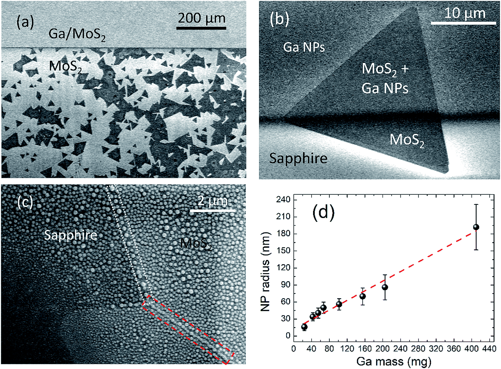 | ||
| Fig. 1 (a–c) Top view SEM images of the MoS2 flakes with Ga NPs with a radius of 41 ± 9 nm. (a) Both regions with Ga and no Ga NPs, (b) single flake of MoS2 in the interface (c) zoom of a region with two Ga/MoS2 flakes. (d) Evolution of the NP radius as a function of the evaporated Ga mass from the histogram of each sample. Red dashed line in (d) is a guide to the eye. | ||
After the MoS2 growth, Ga NPs are deposited on the pristine MoS2 samples by thermal evaporation in a vacuum chamber (see the Experimental part). The central region of each sample was masked for the analysis of the as-deposited pristine MoS2 material. The SEM analysis in Fig. 1 was done with a sample with a NP radius of 41 ± 9 nm grown from 55 mg of Ga that is used as a representative case. In Fig. 1(a), the boundary between pristine MoS2 and Ga NPs/MoS2 regions observed in the upper part is shown. There are flakes that clearly overlap this boundary (Fig. 1(b)) and they are the focus of this work since the optical properties of MoS2 with and without Ga NPs can then be directly compared for the same flakes.
The deposited Ga NPs exhibit a truncated hemispherical shape geometry on top of sapphire with a contact angle around 130°.47 We have not observed significant differences in Ga NP size between deposition on MoS2 and sapphire (Fig. 1(c)). Interestingly, Ga NPs line themselves up along the sapphire/MoS2 (white dotted line) and MoS2/MoS2 (red dashed line) boundaries as can be seen in the dashed regions in Fig. 1(c). Different Ga masses have been evaporated on the MoS2 samples. Fig. 1(d) presents the NP radius that results for each mass. The higher the mass, the higher the NP radius.
Next, we will discuss the optical properties of plasmonic Ga NPs and the influence on the MoS2 optical characteristics, PL and Raman spectra.
Optical characterization of Ga NPs/MoS2
The NP size is directly related to the energy or wavelength of the LSPR.35,48 Due to the typical hemispherical shape of Ga NPs, they can present two plasmon resonance modes. A low-energy mode is along the longest axis and a high-energy mode is due to the shortest axis. They are also known as in-plane (longitudinal) and out-of-plane (transverse) modes, respectively.Spectroscopic Ellipsometry (SE) has been used to track the extinction efficiency ascribed to the LSPR as commonly used in the literature.49Fig. 2(a) shows the imaginary part of the pseudodielectric constant of the sample analyzed by SEM in Fig. 1. A strong absorption about 570 nm is observed that corresponds to the in-plane plasmon resonance mode of the Ga NPs (red dashed line). SE measurements of the MoS2 flakes on sapphire (black solid line), also included in the graph, do not show relevant features apart from the interference that the substrate shows (grey dashed-dotted line). Fig. 2(b) shows SE measurements of different Ga NP radii on MoS2, evidencing the LSPR behavior with NP size. The in-plane mode shifts from the VIS to the infrared (IR) region because of the enlargement of the longest axis of the NPs. On the other hand, the out-of-plane mode lies in the UV region (<200 nm) for most of our cases so it is out of our detectable range. Only for a NP radius of 86 nm (orange dashed-dotted line), the SE measurement shows, apart from the in-plane mode about 1190 nm, a lower intensity band at 344 nm that corresponds to the out-of-plane mode. This set of samples covers the whole near UV-VIS-near IR spectral range with the LSPRs from ∼300 to ∼1200 nm, making this a comprehensive spectral study.
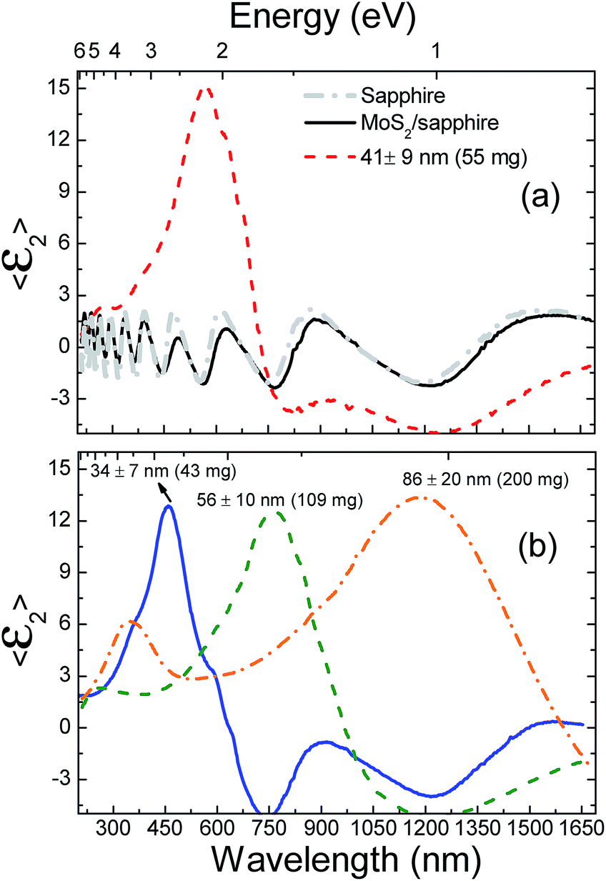 | ||
| Fig. 2 (a) SE measurement of the sample with Ga NPs of 41 nm radius and reference samples of sapphire and the as-grown MoS2/sapphire. (b) SE measurements of different Ga NPs/MoS2 samples where the LSPR shift with the NP radius can be observed. | ||
Fig. 3(a) and (b) show the Raman and PL spectra with and without Ga NPs of the same sample shown in Fig. 1 and 2(a) with 41 nm NP radius. The wavelength of the excitation laser was 532 nm. The black line in Fig. 3(a) represents the Raman spectra of the pristine MoS2 sample. It shows two sharp peaks located at 384 cm−1 and 404 cm−1 that correspond to the E12g phonon vibration and to the A1g transition, respectively.50 The shift between the two main peaks is a common tool to determine the number of layers in MoS2 flakes.20,51 Monolayer MoS2 exhibits a frequency difference of 20 cm−1 between the two modes, as in our case. The sharp peak in the as-grown sample around 415 cm−1 is due to the Raman signal of sapphire.52,53 When Ga is deposited, the maximum peak intensities increase from 262 to 1600 for the E12g and from 240 to 720 for the A1g, which corresponds to an enhancement factor (EF) of 6.1 and 3, respectively. The EF has been calculated from the ratio of the maximum peak intensity with Ga NPs divided by the one without NPs. This improvement of the intensity is due to the SERS effect from Ga NPs, indicating the coupling between both materials.
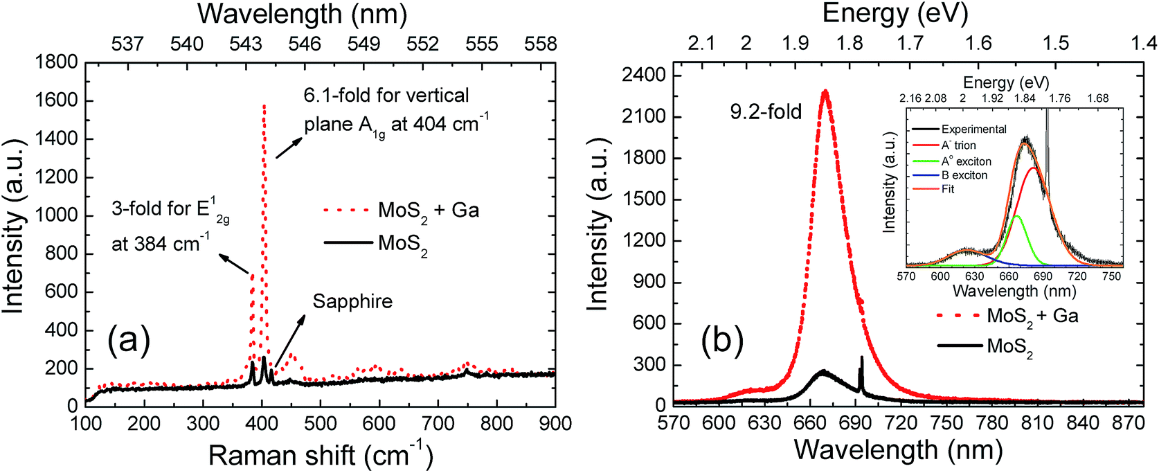 | ||
| Fig. 3 (a) Raman and (b) PL spectra of a MoS2 sample with and without Ga NPs in order to observe the plasmonic enhancement in both cases (excitation at 532 nm). The PL spectra of the pristine MoS2 sample is analyzed in the inset of (b) via fitting with a trion and two excitons. | ||
In the case of the PL spectrum (Fig. 3(b)), the pristine MoS2 sample (black solid line) shows a typical double band that arises from spin–orbit coupling of the valence band electrons at the K symmetry point of the direct bandgap.21 The fitting is illustrated in the inset of Fig. 3(b). The main peak around 1.84 eV is deconvoluted into two peaks that correspond to the A− trion (red line) and A0 exciton (green line) while the other band around 2 eV is due to the B exciton (blue line). The high A peak intensity compared with the B peak also evidences the monolayer character of the measured point. In addition, the sharp decay at wavelengths longer than 680 nm indicates the absence of the indirect bandgap of the monolayer.21 The sharp peak around 693 nm belongs to the sapphire signal.20 Both Raman and PL analysis of the as-grown MoS2 sample indicates the high crystallinity of the flakes.
When Ga NPs are deposited (red dotted line), the maximum intensity of the main peak is increased from 250 to 2320, which corresponds to an EF of 9. Overall, the enhancement implies surface enhanced fluorescence (SEF) which means again that there is coupling between the two materials. The two spectra were normalized and the FWHM of the A band was calculated by fitting with a Gaussian function. In this case, the FWHM is reduced from 28.3 to 25.7 nm or from 124.1 to 112 meV when NPs are deposited.
Once we have studied the LSPR dependence on Ga mass (Fig. 2) and shown SERS and SEF for a representative case (Fig. 3), we can study the role of the LSPR on the PL and Raman EF. Fig. 4(a) shows the average PL EF as a function of the maximum LSPR wavelength (i.e. Ga NP size) for all sets of samples for the 532 nm laser wavelength. The EF was calculated by comparing the PL maximum intensity of pristine monolayer MoS2 to those with Ga NPs above. Each point corresponds to an individual sample, but measured in at least 5 different points in different flakes along the Ga/MoS2 boundary (Fig. 1(b)). Error bars are the standard deviation for each case. It is worth noting that we obtained an EF over 1 for all the cases. Although error bars are considerable in some points, discrepancies between points are a common feature when MoS2 flakes are combined with plasmonic materials.19 However, this feature will be discussed later on. Interestingly, the points with the highest average EF around 5 are samples whose LSPR are 493 and 552 nm, close to the laser wavelength, 532 nm, marked with a green dashed vertical line in Fig. 4(a). However, the samples with a LSPR far away from the laser do not show an average EF higher than 2.5. All these data suggest that the enhanced EF is due to the tuning of the LSPR with the laser wavelength. In other words, the cause of the enhancement is the excitation of the in-plane dipole of the Ga NPs, which can resonate to the same frequency as that of the incident light.
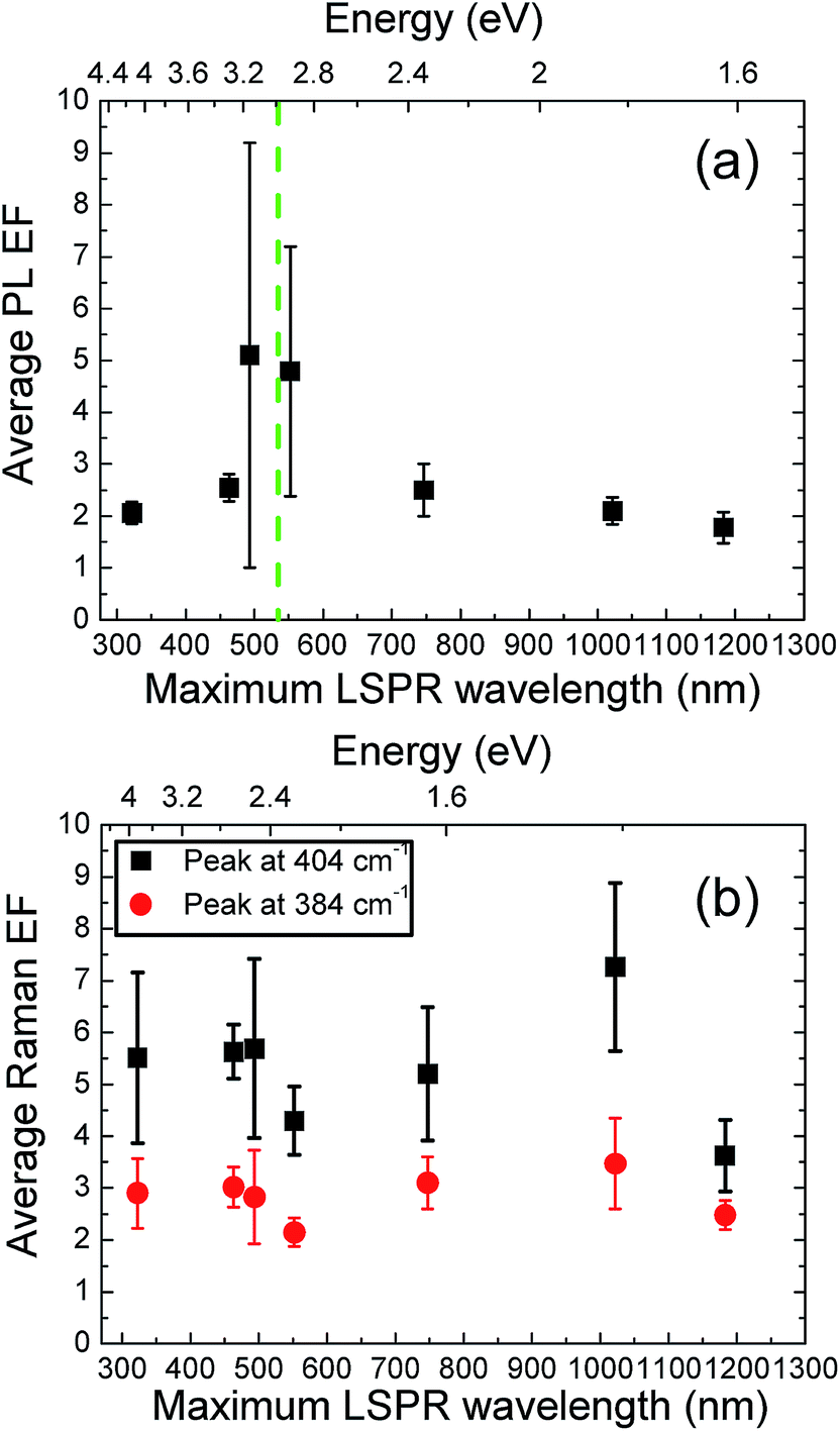 | ||
| Fig. 4 (a) Average PL peak intensity EF of monolayer MoS2 as a function of the LSPR position of Ga NPs. The green line represents the laser wavelength, 532 nm. (b) Average Raman EF of monolayer MoS2 peaks at 384 and 404 cm−1 as a function of the LSPR position of Ga NPs. Error bars indicate the standard deviation. | ||
As mentioned before, in all these experiments, Ga NPs were deposited on top of the MoS2 flakes. This approach has been the most common used in the literature with Au and Ag nanomaterials. They can be deposited by a chemical8,20,21 or physical method22,24,54 but the EF has not been higher than 6.5 except for e-beam lithography Ag NPs whose obtained maximum EF was 12.5.22 Thus, despite Ga being among the so-called poor metals which, in principle, have worse plasmonic properties than noble metals such as Au and Ag, especially in the VIS range, we have obtained an EF in the same order or even higher than the literature with a metallic material (Ga) which supposedly has its best plasmonic performance in the UV region.
In addition to the PL, the same study has been performed with the Raman spectra of the same points analyzed as in Fig. 4(a). Again, the EF was calculated using the ratio between maximum Raman intensities with and without Ga NPs. The results in Fig. 4(b) show that the peak at 404 cm−1 (E12g phonon vibration) is enhanced more than the peak at 384 cm−1 (A1g phonon vibration) for all the samples and, interestingly, both peaks show the same trend. However, there is no clear resonance peak when comparing between points. These results contrast with the observed behavior in the PL analysis shown in Fig. 4(a), suggesting that the physical mechanism regarding the Raman EF is different and should be further analyzed.
PL enhancement origin
As described in the literature,8 the enhancement or modification factor is proportional to the PL collection efficiencies (η), excitation rate (γex) and quantum yield (QY) of the sample with the plasmonic material over their respective values without it (η0, γ0ex and QY0):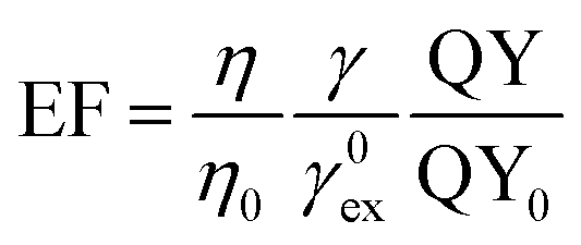
The first term, η, is associated with the radiation directionality and in the case of the dipolar plasmon resonances most energy is radiated along the direction perpendicular to the dipole axis.55 The second term, γex, is related to the electric field  at the laser excitation wavelength. This is enhanced by the Ga NPs, which act as nanoscale optical pumps that increase photon absorption and generation rates of electron–hole pairs in MoS2.8 However, the last term, QY, is understood as an intrinsic MoS2 property, which could also be modified not only with plasmonic material but also with chemical treatments, thickness variation or defect engineering procedures. This factor has also been expressed as an increase of the internal quantum efficiency due to the plasmonic material, which means an increase of spontaneous emission rate.20 In our case, we likely have an increase of the QY in all of the samples since they all show an EF higher than 1 after Ga evaporation and independent of the LSPR. However, only the two samples whose LSPR wavelength overlaps with the laser wavelength exhibit an extra EF that results in a total average EF ∼ 5. Therefore, we attribute this last prominent enhancement of the PL intensity to the LSPR of Ga NPs.
With the goal of demonstrating that the electric field is enhanced by the Ga NPs, we have performed simulations with the DDA method in two scenarios: a sapphire substrate 40 × 100 × 100 nm with a MoS2 monolayer on top and the same system but with a hemispherical Ga NP with a radius of 40 nm and 2 nm of native Ga2O3 on top of the flake as described in the Experimental part. This radius is comparable to the representative case of the SEM analysis in Fig. 1. Fig. 5 shows the calculated spatial distribution of the electric field intensity in a top view (first row) and in a lateral view (second row). The Ga/MoS2/sapphire system (Fig. 5(b)) shows that the electric field is enhanced in the vicinities of the Ga NP. In fact, the in-plane resonance overlaps the MoS2 thickness and the electric field is propagated along the 2D material since it shows hot-spots in the borders of the MoS2. These two factors make the light–matter interaction stronger, leading to an increased PL intensity.
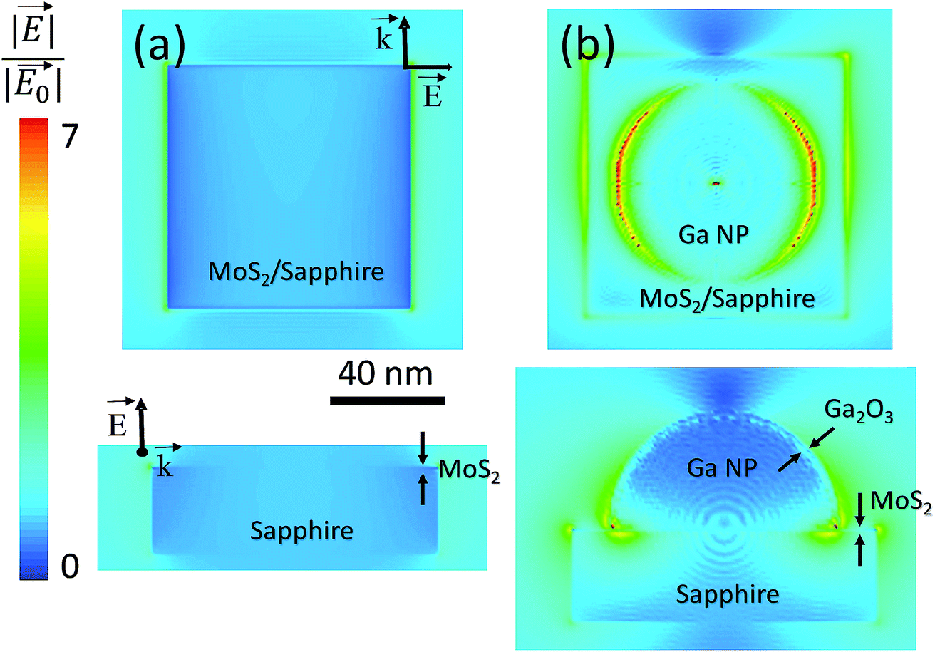 | ||
| Fig. 5 Simulation of the near local electromagnetic field distribution derived from the column (a) MoS2/sapphire system and (b) Ga NP/MoS2/sapphire system. The first row illustrates the top-view while the second row represents a lateral view of each case. The legend indicates the enhancement of the electric field. | ||
In order to get further information about the PL uniformity, we have used a confocal microscope to spectroscopically image μ-PL within the MoS2 flakes of the sample of 43 mg of Ga (LSPR at 463 nm) with a laser wavelength of 488 nm. Each map presents the integrated intensity of the PL peak of each point with a mapping step size of 1 μm. A PL map of a pristine monolayer MoS2 flake is shown in Fig. 6(a). Spatial variations in the intensity are observed across the flake in addition to an increase near the edges (marked with dashed black lines). Intensity variation could be as high as 20% between the centre (orange) and edges (intense yellow, in Fig. 6(a)). These trends are observed in all the flakes that were analyzed in this study and have been previously reported.56,57 The cause is typically ascribed to structural defects that lead to inhomogeneous charge transfer within the flakes. Fig. 6(b) shows the intensity PL map of a MoS2 flake entirely covered with Ga NPs. It can be seen that intensity variations are enhanced due to the plasmonic effect and reach 50%. These observed variations of intensity within the flakes indicate that the choice of the measurement point is crucial when comparing regions within the same flake and is likely the reason for the error bars shown in Fig. 4. In addition, we have constructed a PL map of a flake placed in the boundary with and without Ga NPs (Fig. 6(c)). It mainly shows an upper region with Ga NPs (magenta color) and a lower region (green color) without Ga NPs. Despite the intensity changes in the edges, the effect of the Ga NPs on the PL intensity is clear.
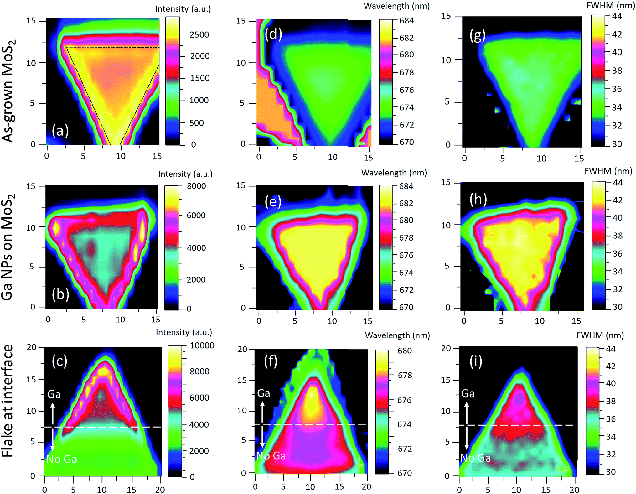 | ||
| Fig. 6 Intensity, wavelength and FWHM PL maps for the three different flakes. (a–c) Intensity images of an isolated as-grown MoS2 flake (a), a totally covered MoS2 flake with Ga NPs (b), and a half covered with Ga NPs (c). (d–f) Images corresponding to the wavelength peak center for the same flakes shown in (a–c). (g–i) Images corresponding to the FWHM of the PL peak of the same flakes shown in (a–c). Axes indicate the horizontal and the vertical distance in μm. | ||
In order to get further information about the PL enhancement origin, we have analyzed, we have analyzed the PL peak wavelength of the same flakes than Fig. 6(a–c) represented in Fig. 6(d–f). The flake without Ga NPs (Fig. 6(d)) shows a PL peak wavelength very homogeneous centered at 675 ± 1 nm while the PL peak of the flake entirely covered with Ga NPs (Fig. 6(e)) is placed at 683 ± 1 nm. Since this PL wavelength shift could be due to differences between flakes, we have mapped the flake located at the interface of Ga NPs/MoS2Fig. 6(f). It can be seen that in the lower half of the flake with no Ga the peak wavelength does not change. However, it shifts around 2–3 nm in the region with Ga NPs (upper half of the flake). This shift might be understood on the basis of the different work functions (ϕ) of Ga (ϕ = 4.25 eV)58 and MoS2 (ϕ = 4.7 eV).12 As a matter of fact, Su et al.56 showed that such a redshift takes place when using metals with a low work function, such as Ag (ϕ = 4.3 eV). They established that a decrease in the relative intensity of the A0 excitons and, therefore, a higher contribution of the A− trion results in a redshift due to the n-type doping produced by the electron injection from the metal (the opposite behavior was found for Au, with ϕ = 5.1 eV).56 Since the Ga work function is also lower than the one of MoS2 (and very similar to the one of Ag) the small redshift found in the map of Fig. 6(f) could be ascribed to the same mechanism. Peak fitting of PL spectra with and without Ga NPs evidences that the A− trion contribution to the overall peak is higher in the region with Ga NPs (not shown).
Furthermore, we have considered how the dielectric screening of the MoS2 could affect the enhancement of the PL. In the literature,59,60 it has been demonstrated that an increase of the dielectric screening increases the PL intensity and reduces the A− trion population, which experimentally results in a blueshift of the exciton-trion PL peak around 680 nm. Since in our case, the A− trion population increases, the dielectric screening may play a minor role in the PL enhancement.
In the last column in Fig. 6(g–i), the FWHM maps of the three scenarios are presented. The flake without Ga NPs in Fig. 6(g) shows a quite homogeneous FWHM of 34 ± 1 nm that increases to 42 ± 1 nm in the flake with Ga NPs in Fig. 6(h). The analysis of the flake half-covered with Ga NPs in Fig. 6(i) reveals a small effect in the FWHM, which only increases 3–4 nm when Ga is deposited (corresponding to 7–10% of the original FWHM).
As an additional confirmation of the EF origin, we have performed PL measurements on the same flake with different laser wavelengths. This procedure has been previously used to confirm that the PL enhancement is related to the LSPR.19Fig. 7(a) shows the microscope images of the chosen flake and the measurement region indicated with dashed squares. Fig. 7(b)–(d) illustrate the PL spectra of the sample whose maximum LSPR is at 463 nm (second point in Fig. 4(a)) with the 445, 532 and 660 nm laser wavelengths, respectively. We would expect a higher EF for the blue (445 nm) laser since the LSPR of this sample is closer in resonance to that laser. The comparison between graphs clearly shows that the EF of the 445 nm laser, 6.7-fold, is higher than the 2.6-fold EF produced by the other lasers with lower energy at the same point. Thus, this comparison is in very good agreement with the discussion shown in Fig. 4(a) and highlights the LSPR as the origin of the highest EF.
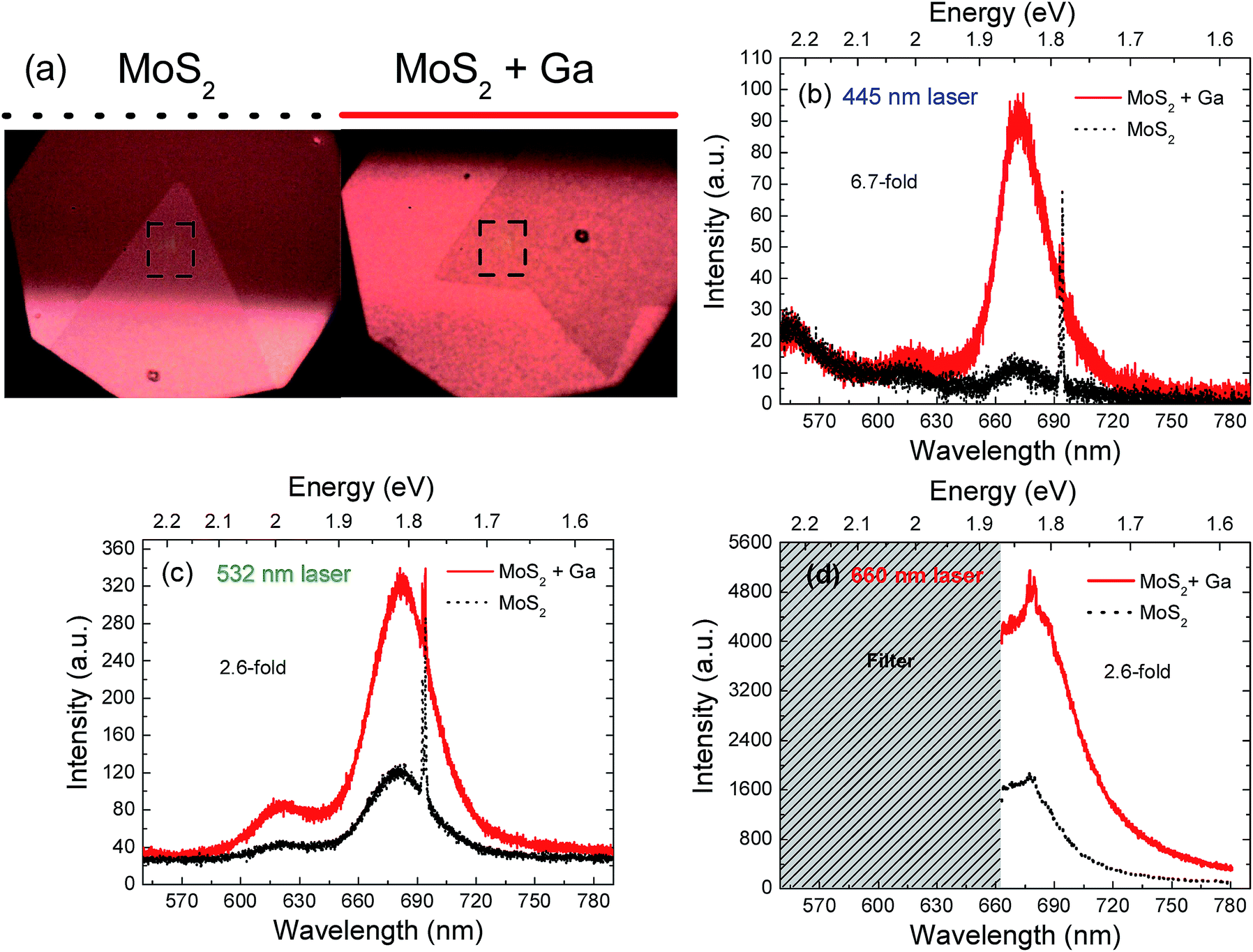 | ||
| Fig. 7 (a) Microscope images of the MoS2 flake without (left) and with Ga NPs (right). Frames indicate the measurement point. PL spectra of monolayer MoS2 with and without Ga NPs for the same flake with laser wavelengths of 445 nm (b), 532 nm (c) and 660 nm (d). The EF and peak wavelength are also indicated for each case. The maximum LSPR wavelength of the deposited Ga NPs is 463 nm. | ||
Conclusions
In summary, our work presents the localized surface plasmon-enhanced PL of monolayer MoS2 using hemispherical Ga NPs. As far as we know, this is the first time that MoS2 PL enhancement is produced by plasmonic metals apart from Au and Ag. We have systematically investigated the PL enhancement with the NP radius and consequently with the LSPR wavelength position. The obtained values are similar to the literature when using NPs on top of MoS2, although other reports have used noble metals and complex methods to obtain the NPs. Furthermore, the use of different excitation wavelengths helped us prove that the origin of the PL enhancement is the LSPR. Additionally, the PL mapping analysis on the Ga–MoS2 flakes shows a PL peak shift likely attributed to a charge transfer mechanism. We have successfully produced a Ga–MoS2 hybrid structure formed by a lithography-free, cost-effective and single-step process through facile thermal evaporation that can be synthesized in large quantities. This work paves the way to the use of other poor metals such as Al, In, Mg and Rh in high-performance plasmon enhanced optoelectronic applications.Conflicts of interest
There are no conflicts to declare.Acknowledgements
We thank Eduardo Ruiz for technical help during the sample preparation. The research is supported by the MINECO (CTQ2014-53334-C2-2-R, MAT2015-65356-C3-1-R and CTQ2017-84309-C2-2-R) and Comunidad de Madrid (NANOAVANSENS ref. S2013/MIT-3029) and UAM-Santander (2017/EEUU/14) projects. ARC acknowledges the Ramón y Cajal program (under contract number RYC-2015-18047). FN acknowledges support from the Marie Sklodowska-Curie grant agreement No. 641899 from the European Union's Horizon 2020 research and innovation programme.Notes and references
- S. Manzeli, D. Ovchinnikov, D. Pasquier, O. V. Yazyev and A. Kis, 2D transition metal dichalcogenides, Nat. Rev. Mater., 2017, 2, 17033 CrossRef CAS.
- F. Ebrahimi and E. Heidari, in Graphene-New Trends and Developments, ed. F. Ebrahimi, InTech, 2015, ch. 1 Search PubMed.
- J.-W. Jiang, Graphene versus MoS2: a short review, Front. Phys., 2015, 10, 287–302 CrossRef.
- A. Splendiani, L. Sun, Y. Zhang, T. Li, J. Kim, C.-Y. Chim, G. Galli and F. Wang, Emerging Photoluminescence in Monolayer MoS2, Nano Lett., 2010, 10, 1271–1275 CrossRef CAS PubMed.
- O. Lopez-Sanchez, D. Lembke, M. Kayci, A. Radenovic and A. Kis, Ultrasensitive photodetectors based on monolayer MoS2, Nat. Nanotechnol., 2013, 8, 497 CrossRef CAS PubMed.
- Z. Li, X. Meng and Z. Zhang, Recent development on MoS2-based photocatalysis: a review, J. Photochem. Photobiol., C, 2018, 35, 39–55 CrossRef CAS.
- M.-L. Tsai, S.-H. Su, J.-K. Chang, D.-S. Tsai, C.-H. Chen, C.-I. Wu, L.-J. Li, L.-J. Chen and J.-H. He, Monolayer MoS2 Heterojunction Solar Cells, ACS Nano, 2014, 8, 8317–8322 CrossRef CAS PubMed.
- W. Gao, Y. H. Lee, R. Jiang, J. Wang, T. Liu and X. Y. Ling, Localized and Continuous Tuning of Monolayer MoS2 Photoluminescence Using a Single Shape-Controlled Ag Nanoantenna, Adv. Mater., 2016, 28, 701–706 CrossRef CAS PubMed.
- K. F. Mak, C. Lee, J. Hone, J. Shan and T. F. Heinz, Atomically Thin MoS2: A New Direct-Gap Semiconductor, Phys. Rev. Lett., 2010, 105, 136805 CrossRef PubMed.
- P. Joo, K. Jo, G. Ahn, D. Voiry, H. Y. Jeong, S. Ryu, M. Chhowalla and B.-S. Kim, Functional Polyelectrolyte Nanospaced MoS2 Multilayers for Enhanced Photoluminescence, Nano Lett., 2014, 14, 6456–6462 CrossRef CAS PubMed.
- H. Nan, Z. Wang, W. Wang, Z. Liang, Y. Lu, Q. Chen, D. He, P. Tan, F. Miao, X. Wang, J. Wang and Z. Ni, Strong Photoluminescence Enhancement of MoS2 through Defect Engineering and Oxygen Bonding, ACS Nano, 2014, 8, 5738–5745 CrossRef CAS PubMed.
- S. Mouri, Y. Miyauchi and K. Matsuda, Tunable Photoluminescence of Monolayer MoS2via Chemical Doping, Nano Lett., 2013, 13, 5944–5948 CrossRef CAS PubMed.
- P. Hu, J. Ye, X. He, K. Du, K. K. Zhang, X. Wang, Q. Xiong, Z. Liu, H. Jiang and C. Kloc, Control of Radiative Exciton Recombination by Charge Transfer Induced Surface Dipoles in MoS2 and WS2 Monolayers, Sci. Rep., 2016, 6, 24105 CrossRef CAS PubMed.
- Y. Li, Z. Li, C. Chi, H. Shan, L. Zheng and Z. Fang, Plasmonics of 2D Nanomaterials: Properties and Applications, Adv. Sci., 2017, 4, 1600430 CrossRef PubMed.
- M. A. García, Surface plasmons in metallic nanoparticles: fundamentals and applications, J. Appl. Phys., 2012, 45, 389501 Search PubMed.
- X. Xu, Y. Shi, X. Liu and M. Sun, Femtosecond dynamics of monolayer MoS2-Ag nanoparticles hybrid probed at 532 nm, Chem. Phys. Lett., 2018, 692, 208–213 CrossRef CAS.
- W. Lin, Y. Shi, X. Yang, J. Li, E. Cao, X. Xu, T. Pullerits, W. Liang and M. Sun, Physical mechanism on exciton-plasmon coupling revealed by femtosecond pump-probe transient absorption spectroscopy, Materials Today Physics, 2017, 3, 33–40 CrossRef.
- X. Yang, H. Yu, X. Guo, Q. Ding, T. Pullerits, R. Wang, G. Zhang, W. Liang and M. Sun, Plasmon-exciton coupling of monolayer MoS2-Ag nanoparticles hybrids for surface catalytic reaction, Materials Today Energy, 2017, 5, 72–78 CrossRef.
- Y. Zeng, X. Li, W. Chen, J. Liao, J. Lou and Q. Chen, Highly Enhanced Photoluminescence of Monolayer MoS2 with Self-Assembled Au Nanoparticle Arrays, Adv. Mater. Interfaces, 2017, 4, 1700739 CrossRef.
- K. C. J. Lee, Y.-H. Chen, H.-Y. Lin, C.-C. Cheng, P.-Y. Chen, T.-Y. Wu, M.-H. Shih, K.-H. Wei, L.-J. Li and C.-W. Chang, Plasmonic Gold Nanorods Coverage Influence on Enhancement of the Photoluminescence of Two-Dimensional MoS2 Monolayer, Sci. Rep., 2015, 5, 16374 CrossRef CAS PubMed.
- A. Sobhani, A. Lauchner, S. Najmaei, C. Ayala-Orozco, F. Wen, J. Lou and N. J. Halas, Enhancing the photocurrent and photoluminescence of single crystal monolayer MoS2 with resonant plasmonic nanoshells, Appl. Phys. Lett., 2014, 104, 031112 CrossRef.
- S. Butun, S. Tongay and K. Aydin, Enhanced Light Emission from Large-Area Monolayer MoS2 Using Plasmonic Nanodisc Arrays, Nano Lett., 2015, 15, 2700–2704 CrossRef CAS PubMed.
- B. Mukherjee, N. Kaushik, R. P. N. Tripathi, A. M. Joseph, P. K. Mohapatra, S. Dhar, B. P. Singh, G. V. P. Kumar, E. Simsek and S. Lodha, Exciton Emission Intensity Modulation of Monolayer MoS2via Au Plasmon Coupling, Sci. Rep., 2017, 7, 41175 CrossRef CAS PubMed.
- J. Yan, C. Ma, P. Liu and G. Yang, Plasmon-Induced Energy Transfer and Photoluminescence Manipulation in MoS2 with a Different Number of Layers, ACS Photonics, 2017, 4, 1092–1100 CrossRef CAS.
- G. V. Naik, V. M. Shalaev and A. Boltasseva, Alternative Plasmonic Materials: Beyond Gold and Silver, Adv. Mater., 2013, 25, 3264–3294 CrossRef CAS PubMed.
- F. Hubenthal, T. Ziegler, C. Hendrich, M. Alschinger and F. Träger, Tuning the surface plasmon resonance by preparation of gold-core/silver-shell and alloy nanoparticles, Eur. Phys. J. D, 2005, 34, 165–168 CrossRef CAS.
- J. M. McMahon, G. C. Schatz and S. K. Gray, Plasmonics in the ultraviolet with the poor metals Al, Ga, In, Sn, Tl, Pb, and Bi, Phys. Chem. Chem. Phys., 2013, 15, 5415–5423 RSC.
- A. G. Marín, T. G. Mendiola, C. N. Bernabeu, M. J. Hernández, J. Piqueras, J. L. Pau, F. Pariente and E. Lorenzo, Gallium plasmonic nanoparticles for label-free DNA and single nucleotide polymorphism sensing, Nanoscale, 2016, 8, 9842–9851 RSC.
- A. G. Marín, M. J. Hernández, E. Ruiz, J. M. Abad, E. Lorenzo, J. Piqueras and J. L. Pau, Immunosensing platform based on gallium nanoparticle arrays on silicon substrates, Biosens. Bioelectron., 2015, 74, 1069–1075 CrossRef PubMed.
- B. F. Soares, F. Jonsson and N. I. Zheludev, All-optical phase-change memory in a single gallium nanoparticle, Phys. Rev. Lett., 2007, 98, 153905 CrossRef PubMed.
- A. V. Krasavin and N. I. Zheludev, Active plasmonics: controlling signals in Au/Ga waveguide using nanoscale structural transformations, Appl. Phys. Lett., 2004, 84, 1416–1418 CrossRef CAS.
- P. C. Wu, C. G. Khoury, T.-H. Kim, Y. Yang, M. Losurdo, G. V. Bianco, T. Vo-Dinh, A. S. Brown and H. O. Everitt, Demonstration of Surface-Enhanced Raman Scattering by Tunable, Plasmonic Gallium Nanoparticles, J. Am. Chem. Soc., 2009, 131, 12032–12033 CrossRef CAS PubMed.
- Y. Yang, J. M. Callahan, T.-H. Kim, A. S. Brown and H. O. Everitt, Ultraviolet Nanoplasmonics: A Demonstration of Surface-Enhanced Raman Spectroscopy, Fluorescence, and Photodegradation Using Gallium Nanoparticles, Nano Lett., 2013, 13, 2837–2841 CrossRef CAS PubMed.
- S. Catalán-Gómez, C. Bran, N. Gordillo, F. Nucciarelli, M. Vázquez, J. L. Pau and A. Redondo-Cubero, Self-assembly of highly ordered plasmonic gallium nanoparticles driven by nanopatterning, Nano Futures, 2018, 2, 041001 CrossRef.
- S. Catalán-Gómez, A. Redondo-Cubero, F. J. Palomares, F. Nucciarelli and J. L. Pau, Tunable plasmonic resonance of gallium nanoparticles by thermal oxidation at low temperatures, Nanotechnology, 2017, 28, 405705 CrossRef PubMed.
- J. L. Pau, A. García-Marín, M. J. Hernández, E. Lorenzo and J. Piqueras, Optical biosensing platforms based on Ga–graphene plasmonic structures on Cu, quartz and SiO2/Si substrates, Phys. Status Solidi B, 2016, 253, 664–670 CrossRef CAS.
- C. Yi, T.-H. Kim, W. Jiao, Y. Yang, A. Lazarides, K. Hingerl, G. Bruno, A. Brown and M. Losurdo, Evidence of Plasmonic Coupling in Gallium Nanoparticles/Graphene/SiC, Small, 2012, 8, 2721–2730 CrossRef CAS PubMed.
- S. Catalán-Gómez, A. Redondo-Cubero, F. J. Palomares, L. Vázquez, E. Nogales, F. Nucciarelli, B. Méndez, N. Gordillo and J. L. Pau, Size-selective breaking of the core–shell structure of gallium nanoparticles, Nanotechnology, 2018, 29, 355707 CrossRef PubMed.
- B. T. Draine and P. J. Flatau, Discrete-Dipole Approximation For Scattering Calculations, J. Opt. Soc. Am. A, 1994, 11, 1491–1499 CrossRef.
- J. Feser and A. N. Sobh, DDSCAT Convert: A Target Generation Tool, 2016, https://nanohub.org/resources/ddaconvert Search PubMed.
- B. T. Draine and P. J. Flatau, User Guide for the Discrete Dipole Approximation Code DDSCAT 7.2, 2012 Search PubMed.
- M. W. Knight, T. Coenen, Y. Yang, B. J. M. Brenny, M. Losurdo, A. S. Brown, H. O. Everitt and A. Polman, Gallium Plasmonics: Deep Subwavelength Spectroscopic Imaging of Single and Interacting Gallium Nanoparticles, ACS Nano, 2015, 9, 2049–2060 CrossRef CAS PubMed.
- M. F. Al-Kuhaili, S. M. A. Durrani and E. E. Khawaja, Optical properties of gallium oxide films deposited by electron-beam evaporation, Appl. Phys. Lett., 2003, 83, 4533–4535 CrossRef CAS.
- A. K. Harman, S. Ninomiya and S. Adachi, Optical constants of sapphire (α-Al2O3) single crystals, J. Appl. Phys., 1994, 76, 8032–8036 CrossRef CAS.
- A. R. Beal and H. P. Hughes, Kramers-Kronig analysis of the reflectivity spectra of 2H-MoS2, 2H-MoSe2 and 2H-MoTe2, J. Phys. C: Solid State Phys., 1979, 12, 881 CrossRef CAS.
- L. Yi-Hsien, Z. Xin-Quan, Z. Wenjing, C. Mu-Tung, L. Cheng-Te, C. Kai-Di, Y. Ya-Chu, W. J. Tse-Wei, C. Chia-Seng, L. Lain-Jong and L. Tsung-Wu, Synthesis of Large-Area MoS2 Atomic Layers with Chemical Vapor Deposition, Adv. Mater., 2012, 24, 2320–2325 CrossRef PubMed.
- M. Losurdo, A. Suvorova, S. Rubanov, K. Hingerl and A. S. Brown, Thermally stable coexistence of liquid and solid phases in gallium nanoparticles, Nat. Mater., 2016, 15, 995–1002 CrossRef CAS PubMed.
- P. C. Wu, T.-H. Kim, A. S. Brown, M. Losurdo, G. Bruno and H. O. Everitt, Real-time plasmon resonance tuning of liquid Ga nanoparticles by in situ spectroscopic ellipsometry, Appl. Phys. Lett., 2007, 90, 103119 CrossRef.
- M. Losurdo, Applications of ellipsometry in nanoscale science: needs, status, achievements and future challenges, Thin Solid Films, 2011, 519, 2575–2583 CrossRef CAS.
- H. Li, Q. Zhang, C. C. R. Yap, B. K. Tay, T. H. T. Edwin, A. Olivier and D. Baillargeat, From Bulk to Monolayer MoS2: Evolution of Raman Scattering, Adv. Funct. Mater., 2012, 22, 1385–1390 CrossRef CAS.
- C. Lee, H. Yan, L. E. Brus, T. F. Heinz, J. Hone and S. Ryu, Anomalous Lattice Vibrations of Single- and Few-Layer MoS2, ACS Nano, 2010, 4, 2695–2700 CrossRef CAS PubMed.
- K.-K. Liu, W. Zhang, Y.-H. Lee, Y.-C. Lin, M.-T. Chang, C.-Y. Su, C.-S. Chang, H. Li, Y. Shi, H. Zhang, C.-S. Lai and L.-J. Li, Growth of Large-Area and Highly Crystalline MoS2 Thin Layers on Insulating Substrates, Nano Lett., 2012, 12, 1538–1544 CrossRef CAS PubMed.
- M. Kadleíková, J. Breza and M. Veselý, Raman spectra of synthetic sapphire, Microelectron. J., 2001, 32, 955–958 CrossRef.
- Y. Yu, Z. Ji, S. Zu, B. Du, Y. Kang, Z. Li, Z. Zhou, K. Shi and Z. Fang, Ultrafast Plasmonic Hot Electron Transfer in Au Nanoantenna/MoS2 Heterostructures, Adv. Funct. Mater., 2016, 26, 6394–6401 CrossRef CAS.
- B. Paolo, H. Jer-Shing and H. Bert, Nanoantennas for visible and infrared radiation, Rep. Prog. Phys., 2012, 75, 024402 CrossRef.
- W. Su, N. Kumar, S. Mignuzzi, J. Crain and D. Roy, Nanoscale mapping of excitonic processes in single-layer MoS2 using tip-enhanced photoluminescence microscopy, Nanoscale, 2016, 8, 10564–10569 RSC.
- W. Bao, N. J. Borys, C. Ko, J. Suh, W. Fan, A. Thron, Y. Zhang, A. Buyanin, J. Zhang, S. Cabrini, P. D. Ashby, A. Weber-Bargioni, S. Tongay, S. Aloni, D. F. Ogletree, J. Wu, M. B. Salmeron and P. J. Schuck, Visualizing nanoscale excitonic relaxation properties of disordered edges and grain boundaries in monolayer molybdenum disulfide, Nat. Commun., 2015, 6, 7993 CrossRef CAS PubMed.
- J. Speight, Lange's Handbook of Chemistry, McGraw-Hill Professional, Boston, 2004 Search PubMed.
- Y. Lin, X. Ling, L. Yu, S. Huang, A. L. Hsu, Y.-H. Lee, J. Kong, M. S. Dresselhaus and T. Palacios, Dielectric Screening of Excitons and Trions in Single-Layer MoS2, Nano Lett., 2014, 14, 5569–5576 CrossRef CAS PubMed.
- M. Wang, W. Li, L. Scarabelli, B. B. Rajeeva, M. Terrones, L. M. Liz-Marzán, D. Akinwande and Y. Zheng, Plasmon–trion and plasmon–exciton resonance energy transfer from a single plasmonic nanoparticle to monolayer MoS2, Nanoscale, 2017, 9, 13947–13955 RSC.
| This journal is © The Royal Society of Chemistry 2019 |