
 Open Access Article
 This Open Access Article is licensed under a
 Creative Commons Attribution 3.0 Unported Licence
Developing colloidal nanoparticles for inkjet printing of devices with optical properties tuneable from the UV to the NIR†
Jonathan S. Austin a,
Weitong Xiaoab,
Feiran Wanga,
Nathan D. Cottamc,
Geoffrey Riversa,
Ellie B. Warda,
Tyler S. S. Jamesc,
Weiling Luanb,
Christopher J. Tucka,
Richard Haguea,
Oleg Makarovskyc and
Lyudmila Turyanska*a
a,
Weitong Xiaoab,
Feiran Wanga,
Nathan D. Cottamc,
Geoffrey Riversa,
Ellie B. Warda,
Tyler S. S. Jamesc,
Weiling Luanb,
Christopher J. Tucka,
Richard Haguea,
Oleg Makarovskyc and
Lyudmila Turyanska*a
aCentre for Additive Manufacturing, Faculty of Engineering, University of Nottingham, Jubilee Campus, Nottingham, NG8 1BB, UK. E-mail: Lyudmila.Turyanska@nottingham.ac.uk
bCPCIF Key Laboratory of Advanced Battery Systems and Safety, School of Mechanical and Power Engineering, East China University of Science and Technology, Shanghai 200237, China
cSchool of Physics and Astronomy, University of Nottingham, Nottingham, NG7 2RD, UK
First published on 27th June 2024
Abstract
Colloidal low-dimensional photo-sensitive nanomaterials have attracted significant interest for optoelectronic device applications where inkjet printing offers a high accuracy and low waste route for their deposition on silicon-based, as well as flexible, devices. However, to achieve photodetection and displays with absorption and emission tuneable across the range from the ultraviolet (UV) to the near infrared (NIR), the availability of printable optically active materials needs to be addressed. In this work we develop printable ink formulations of graphene quantum dots (GQDs), NaYF4:(20%Yb and/or 2%Er doped) upconverting nanoparticles (UCNPs), and PbS quantum dots (QDs) and demonstrate their use in devices such as graphene-based photodetectors and fluorescent displays. The ink formulations, printing strategies and post-deposition techniques were developed and optimised to enable the deposition of photo-sensitive nanomaterial layers in a controllable manner onto flexible polymeric, glass and silicon substrates. The nanomaterials retained their properties post deposition, as we exemplify by photosensitisation of single layer graphene (SLG) photodetector devices, with spectral responsivity tuneable from the UV for GQD/SLG to the NIR for UCNP/SLG and PbS/SLG devices, with photoresponsivity up to R ∼ 103 A W−1. Fluorescent displays were also demonstrated consisting of CsPbBr3 perovskite nanocrystals and UCNPs inkjet printed onto flexible transparent substrates, for selective sensing of UV and NIR light. This work successfully expands the material library of printable optically active materials and demonstrates their potential for printed optoelectronics, including flexible devices.
Introduction
Colloidal low-dimensional optically active nanoparticles are attracting significant attention for device applications such as solar cells,1 LED/displays,2,3 and photodetectors4,5 due to their band gap tunability across a wide range of the electromagnetic spectrum from the UV to the NIR.6 Inkjet printing is of particular interest and can offer manufacturing solutions for high accuracy and low waste deposition of nanomaterials onto a variety of substrates from silicon compatible wafers to flexible polymeric films,7–13 which cannot be easily achieved with traditional manufacturing. To date, several reports demonstrated inkjet deposition of colloidal nanoparticles. For example, graphene detectors with optically active layers, deposited using additive manufacturing technologies, were demonstrated with colloidal 0D quantum dots (e.g. ZnO QDs,12 PbS QDs,7,8 HgTe QDs9) and perovskite nanoparticles.10,11 For applications requiring narrow absorption, particularly in the NIR, lanthanide doped upconverting nanoparticles (UCNP) are being investigated,14,15 such as NaYF4:20%Yb3+, 2%Er3+; with an absorption peak centred at 976 nm and a full width at half maximum (FWHM) of 15 nm,16 they are of interest for a range of applications from bioimaging to fluorescent displays.14,15,17,18 More recently, carbon based materials, such as graphene quantum dots (GQDs), have emerged as biocompatible nanomaterials that are optically active in the UV range.19 However the availability of printable optically active materials is limited and requires bespoke ink formulations. To address the limited availability of inks of functional materials for inkjet manufacturing of optoelectronic devices, there is a need to explore strategies for versatile ink formulations that are applicable to nanoparticles with different composition. This will also allow new opportunities for the exploration of combined multiple nanoparticles in a single device to achieve specific spectral sensitivities.Here we develop printable ink formulations of GQDs, NaYF4:(20%Yb and/or 2%Er doped) UCNPs, and PbS QDs inks and demonstrate their use for devices such as graphene-based photodetectors and fluorescent displays. By developing and optimising ink formulations, printing strategies and post-deposition techniques, photo-sensitive nanomaterial layers were deposited in a controllable manner onto glass, silicon and flexible polymeric substrates, and were also integrated into printed heterostructures. We exemplify the potential of our nanomaterial ink formulations by using them as surface functionalisation layers in single layers graphene (SLG) photodetectors, where photoresponsivity up to R ∼ 103 A W−1 can be achieved and spectral range is tuneable from the UV for GQD/SLG to the NIR for UCNP/SLG and PbS/SLG devices. We also explore deposition of multiple inks into one structure, illustrating that devices such as fluorescent displays can be produced, as we report here with CsPbBr3 perovskite NCs and UCNP inkjet printed onto flexible transparent substrates. This work expands the material library of printable optically active nanomaterials and showcases their prospective use for printed optoelectronics, including flexible devices.
Results and discussion
For this work we selected a number of optically active colloidal nanomaterials including water dispersed GQDs and PbS QDs as well as non-polar organic solvent dispersed UCNPs and perovskite NCs10 (Fig. 1a). Optical properties of the nanoparticles depend on their size and composition, and our four selected materials have absorption and emission that is tuneable across the wavelength range from the UV to the NIR. This selection allows us to establish protocols for the formulation and inkjet deposition of water-based and non-polar solvent-based nanoparticle inks (Fig. 1a–c). Inkjet printing offers a high degree of geometric freedom, where versatile designs can be deposited in a drop-on-demand manner, also bringing material saving benefits. Here we demonstrate these advantages by printing designs from GQD honeycomb lattices to CsPbBr3 and PbS QD geometric shapes to recreating building outlines with UCNPs (Fig. 1d–g).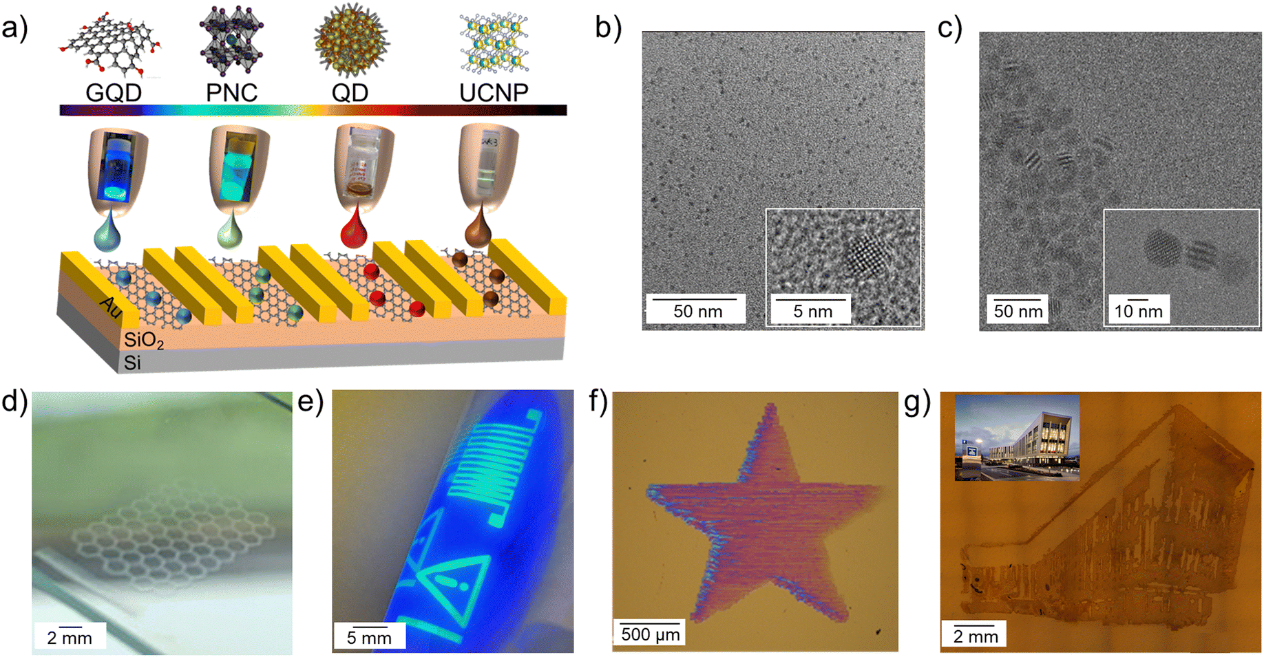 | ||
| Fig. 1 (a) Schematic diagram of nanoparticles formulated for inkjet printing, including graphene QDs sensitive in the UV range, perovskite NCs sensitive in the visible range, and semiconductor QDs and upconverting NPs sensitive in the NIR range. Representative TEM and (insets) HR TEM images of (b) PbS QDs and (c) β-NaYF4:20%Yb3+, 2%Er3+ UCNPs. Optical images of (d) 5 printed layers of GQD-PVP in honeycomb pattern (14 × 10 mm pattern size) on glass, (e) 5 printed layers of CsPbBr3 NCs on PEN (32 × 10 mm pattern size), with green fluorescence under λex = 365 nm illumination, (f) 4 printed layers of PbS QD in a star pattern on Si/SiO2 substrate, and (g) 5 printed layers of UCNP pattern on flexible Kapton substrate printed in the design of Advanced Manufacturing Building at the University of Nottingham (photo in the inset). | ||
Ink formulations need to satisfy the rheological requirements for inkjet deposition,20 while ensuring compositional and colloidal stability of the nanoparticles. For water based inks, GQDs (size of < 10 nm) and PbS QDs capped with dihydrolipoic-acid polyethylene-glycol-amine (DHLA-PEG400-NH2) ligands (average diameter d = 3.0 ± 1.0 nm)21 were used (Fig. 1b and SI1, Fig. S1, ESI†). To formulate the inks, QDs were added to a mixture of water, butanol and isopropyl alcohol (IPA) (8.6![[thin space (1/6-em)]](https://www.rsc.org/images/entities/char_2009.gif) :0.32:1.1 v/v) to form a solution with final QD concentration of 1 mg mL−1. The solvents were selected for ink formulation based on their distinct boiling points and surface tensions (80 °C, 100 °C, 120 °C and 22 mN m−1, 72 mN m−1, 24 mN m−1 for IPA, water, and butanol, respectively) in order to inhibit the coffee ring effect.22 The inks had an inverse Ohnesorge number of Z = 31.5 for PbS QDs and Z = 19 for GQDs, which allowed consistent drop formation without any satellite droplets or instability over time. The drop formation and contact angle analysis were performed (SI1, Fig. S2, ESI†). As expected, the contact angle for water-based inks was ∼40°, while organic solvent-based inks had low contact angles of < 5° on Si/SiO2 substrates. The printing was performed on a Dimatix inkjet printer in air with a substrate temperature of Tsubstrate = 60 °C to facilitate solvent evaporation during printing. After printing, films were annealed in air at 100 °C for 30 minutes to remove any residual solvents.
:0.32:1.1 v/v) to form a solution with final QD concentration of 1 mg mL−1. The solvents were selected for ink formulation based on their distinct boiling points and surface tensions (80 °C, 100 °C, 120 °C and 22 mN m−1, 72 mN m−1, 24 mN m−1 for IPA, water, and butanol, respectively) in order to inhibit the coffee ring effect.22 The inks had an inverse Ohnesorge number of Z = 31.5 for PbS QDs and Z = 19 for GQDs, which allowed consistent drop formation without any satellite droplets or instability over time. The drop formation and contact angle analysis were performed (SI1, Fig. S2, ESI†). As expected, the contact angle for water-based inks was ∼40°, while organic solvent-based inks had low contact angles of < 5° on Si/SiO2 substrates. The printing was performed on a Dimatix inkjet printer in air with a substrate temperature of Tsubstrate = 60 °C to facilitate solvent evaporation during printing. After printing, films were annealed in air at 100 °C for 30 minutes to remove any residual solvents.
Continuous printed films of PbS QDs were achieved on Kapton, polyethylene naphthalate (PEN), glass and Si/SiO2 substrates after the deposition of the number of printed layers nL = 4 (Fig. 1f). Note that a single printed droplet has a spot size of ∼30 μm on Si/SiO2 (Fig. S2, ESI†). Importantly, the optical properties of the PbS QDs were preserved following ink formulation and the inkjet deposition process, with PbS QD films displaying an optical emission peak centred at λ ∼ 990 nm (SI1, Fig. S1b, ESI†).
For GQDs, de-wetting was observed on Kapton, PEN and Si/SiO2 substrates; printed films formed many isolated islands with a diameter ∼15 μm (Fig. S2, ESI†). The difference in wetting between the two inks is due to the PEG ligands on the PbS QDs resulting in reduced viscosity and increased surface tension of the ink. More favourable wetting was observed for the GQD ink on glass, where a single printed droplet has a diameter of ∼40 μm and continuous films were achieved after the deposition of nL = 5 printed layers. However, non-optimal wetting still caused non-uniformity in printed films. This was accompanied by quenching of PL emission, due to aggregation of GQDs. To ensure colloidal stability and dispersion of the GQDs in the ink, and to improve substrate wetting, a small amount (0.86 mg mL−1) of the polymers PEG or polyvinylpyrrolidone (PVP) was added to form the GQD-PEG and GQD-PVP inks, respectively. The inks had Z = 47 for GQD-PEG and Z = 21 for GQD-PVP, which allowed consistent jetting to be achieved. The GQD-PVP ink displayed the best wetting and film uniformity; a single printed droplet left a spot size of ∼30 μm on Si/SiO2 and Kapton substrates, and continuous GQD films were printed on Si/SiO2, glass, Kapton and PEN substrates after the deposition of nL = 5 printed layers (Fig. 1d and 2a). Some non-uniformity of the intensity of optical emission was revealed by PL mapping (SI1, Fig. S3, ESI†), likely due to the high surface tension and low viscosity of the ink, which causes a capillary force that pulls the ink towards the start of the printing swathe (left) during drying.23 Both printed films, GQD-PEG and GQD-PVP, displayed visible fluorescence and PL peak centred at λ = 485 nm under UV excitation (λex = 365 nm) (Fig. 2a and b). For GQD films stored at ambient conditions, a PL peak was also recorded at λ = 610 nm which is attributed to QD oxidation. The emission and absorption spectra of the GQD-PEG and GQD-PVP do not show any evidence of QD oxidation (Fig. 2b and SI1, Fig. S3c, ESI†). Hence, the addition of these polymers into the ink formulation not only improves the uniformity and optical properties of the printed films, but also prevents the QDs oxidation, enhancing their environmental stability.
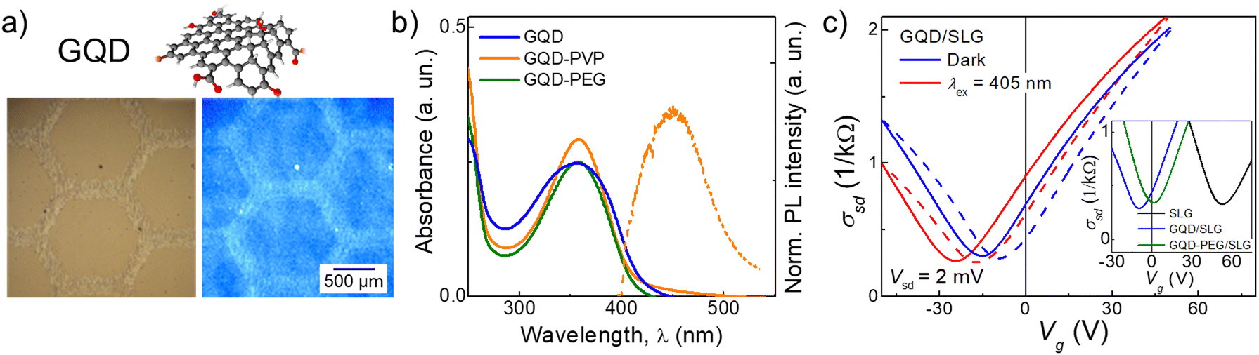 | ||
| Fig. 2 (a) Optical image of 5 printed layers of GQD-PVP film in honeycomb pattern on glass substrate under white light (left) and under illumination with λex = 365 nm (right). (b) Optical absorbance (solid lines) and PL intensity (dashed line) of printed GQD, GQD-PEG, and GQD-PVP films. (c) Dependence of GQD/SLG source–drain current, σsd, on applied gate voltage, Vg, in the dark (blue), and under constant (λex = 405 nm, P = 56.6 W m−2) excitation (red). Vg is swept from −50 V to +50 V (+90 V for SLG) (solid lines) and then back to −50 V (dashed lines) (Vsd = 2 mV, sweep rate = 0.17 V s−1). Inset: Dependence of σsd on Vg for SLG, before and after deposition of GQDs and GQDs-PEG on top. Vg swept from −50 V to +50 V (+90 V for SLG). | ||
Nanomaterials dispersed in non-polar solvents were formulated following the modified protocol, which we developed for perovskite NCs.10 We used CsPbBr3 NCs (size ∼11 ± 1 nm)10 (Fig. 1e), NaYF4:20%Yb, 2%Er UCNPs, (Fig. 1g), and NaYF4:2%Er UCNPs synthesized by a thermal coprecipitation method (diameter d = 18.8 ± 1.7 nm) (Fig. 1c and SI1, Fig. S4, ESI†).24 UCNP inks were formulated in a mixture of hexane, cyclohexanone, and terpineol (1:3:1 v/v) with a final UCNP concentration of 20 mg mL−1 and inverse Ohnesorge number of Z = 7. This is lower than the Z = 17 observed in the perovskite ink, which is due to the increased nanoparticle size and higher concentration of the UCNPs leading to a greater ink viscosity. A single droplet of UCNPs on Si/SiO2 substrate has a diameter of ∼35 μm, comparable to the drop of perovskite ink (∼40 μm). Higher nanoparticle loading in the UCNP ink enabled deposition of continuous thin films with a single printed layer, as well as films produced with nL ≥10. Both UCNPs inks showed a sharp absorption peak at 980 nm and the printed films displayed fluorescence under λex = 980 nm illumination with two PL peaks centered at 540 nm and 654 nm (SI1, Fig. S4b, ESI†), confirming that the optical properties of the UCNP are retained in inkjet printed films. The printed NaYF4:20%Yb 2%Er UCNP films displayed green fluorescence and printed NaYF4:2%Er UCNP films displayed orange fluorescence due to the different ratios of PL peak intensities. Raman spectroscopy mapping indicated that the uniformity of the UCNPs distribution in the printed film is increased with increasing number of printed layers from nL = 1 to 10 (SI1, Fig. S5, ESI†), however, small areas of UCNP aggregates are observed, which can be attributed to the coffee ring effect.
To demonstrate the potential of our nanoparticle inks for device application, we explore their performance in two types of devices: photodetectors and fluorescent displays. For photon detection, the nanoparticle inks were printed onto a SLG device, discussed below, and act as a photosensitive layer. In this type of detector, the spectral range is defined by the absorption profile of the nanoparticles, and the photoresponsivity is affected by the transfer efficiency of photoexcited charges from the nanoparticles into graphene. Other parameters, such as nanoparticle PL lifetime, surface doping and carrier mobility of graphene also contribute to device performance.25,26
Graphene field effect transistors (GFET) fabricated using CVD grown SLG placed on Si/SiO2 substrate (SiO2 layer thickness 285 nm)27 were used as platforms for ink deposition. Pristine GFET devices demonstrated p-type conductivity with Dirac point (minimum conductivity) at Vg ≈ +50 V (Fig. 2c, inset, black line) corresponding to p ≈ 4 × 1012 cm−2 and mobility μ ≈ 2000 cm2 V−1 s−1, as is typical for this type of device.27 Following the deposition of nanoparticle inks, the position of the Dirac point shifted toward negative gate voltages suggesting a strong n-type surface doping effect. For example, the Dirac point of a SLG device shifted from Vg = +55 V to Vg = −5 V (n = 3.6 × 1011 cm−2) after deposition of GQD ink (Fig. 2c, inset, blue line). The electron mobility increased from μe = 2100 cm2 V−1 s−1 to μe = 3500 cm2 V−1 s−1, while hole mobility decreased from μh = 3500 cm2 V−1 s−1 to μh = 2300 cm2 V−1 s−1. We note that the difference in carrier mobility is likely due to the presence of both positive and negative impurities in SLG, which has different scattering rates for electrons and holes.
Deposition of GQD-PEG and GQD-PVP also resulted in surface doping and affected carrier mobility in graphene (Fig. 2c, inset, green line and SI2 Fig. S6, ESI†). We note that these changes are accompanied by an increase in hysteresis of σsd(Vg), which is affected by the sweep rate (SI2, Fig. S7, ESI†), and was previously observed in perovskite/graphene detectors and attributed to the slow charge accumulation in the layer of deposited nanocrystals acting as a top gate.25,26 To explore the charge dynamics of these devices, AC electrical measurements were performed (SI2, Fig. S7, ESI†), revealing constant capacitance of C = 16 pF for all frequencies in the range 10 Hz–100 kHz measured for pristine SLG GFET. Following deposition of GQD and GQD-PEG, the capacitance increased to C > 100 pF at low frequencies (f < 50 Hz), but remained similar, C ≈ 20 pF, at high frequencies (f > 10 kHz). This result confirms that charge accumulation in the top QD or nanocrystal layer can be observed only at low frequencies due to slow charge transfer between the SLG and nanoparticles.25 σsd(Vg) dependence of GQD/SLG devices was also studied under constant illumination with λex = 405 nm (Fig. 2c) which caused a further n-type shift in the position of the Dirac point by ∼−10 V. This photo-response is attributed to the transfer of photoexcited electrons from the GQDs into graphene, as was observed previously in perovskite/SLG devices.10,25 The largest photo-response was recorded close to the Dirac point, at Vg = −4 V during forward Vg sweeps.
Similar results were observed for SLG devices decorated with PbS QDs and UCNP, however, the magnitude of their effect on the electrical properties of the SLG is different, which is likely due to the different sizes of the nanoparticles and capping ligands used. It is known that for insulating nanoparticle films, the surface doping arises due to charge transfer from the nanoparticles in the immediate vicinity to the SLG, hence, the nanoparticle size and the packing density can affect the magnitude of the observed effect.28 Indeed, for SLG devices decorated with PbS QDs (QD diameter ∼3 nm; nL = 5), a large n-type shift of the Dirac point was observed from Vg = +30 V to Vg = −40 V (corresponding to charge transfer Δn = 5 × 1012 cm−2). A smaller positive shift of the minimum of the σsd(Vg) by Vg ∼ 10 V (Δn = 7 × 1011 cm−2) was observed for the NaYF4:20%Yb 2%Er UCNP decorated device (NP diameter 19 nm; nL = 2). These concentrations are in qualitative agreement with the surface density of the used QDs calculated assuming a hexagonal close packed (hcp) lattice (filling factor 0.74): 4.2 × 1012 cm−2 for PbS QDs (size with capping ligands ∼5.5 nm) and 2.9 × 1011 cm−2 for UCNP (size with capping ligands ∼21 nm).
These surface decorated FETs are photosensitive. The GQD decorated devices are photosensitive in the UV range, with responsivity R up to 5.3 × 10² A W−1 recorded with λex = 405 nm (Fig. 3a) and response time of τON = 50 s and τOFF = 800 s (SI2, Fig. S8a, ESI†). The long response times are ascribed to the slow QD-SLG charge transfer and resulting photo-gating effect,25 which is also associated with very large (≫1 A W−1) responsivity due to long (>1 s) life time of the photoexcited charges. Among the three studied GQD formulations, the highest photo-response R = 5.3 × 10² A W−1 was measured for the GQD-PEG/SLG, compared to R = 1.7 × 10² A W−1 for the GQD/SLG (Fig. 3a), which can be attributed to the beneficial effects of PEG preventing the oxidation of the QDs. It should be noted that the length of the polymer used can affect the charge transfer process by creating a dielectric barrier. Since we used short chain PEG (Mw = 1000 Da), this has not affected the charge transfer, unlike longer chain PVP (Mw = 40000 Da), where lower maximum responsivity R ∼ 28 A W−1 was observed.
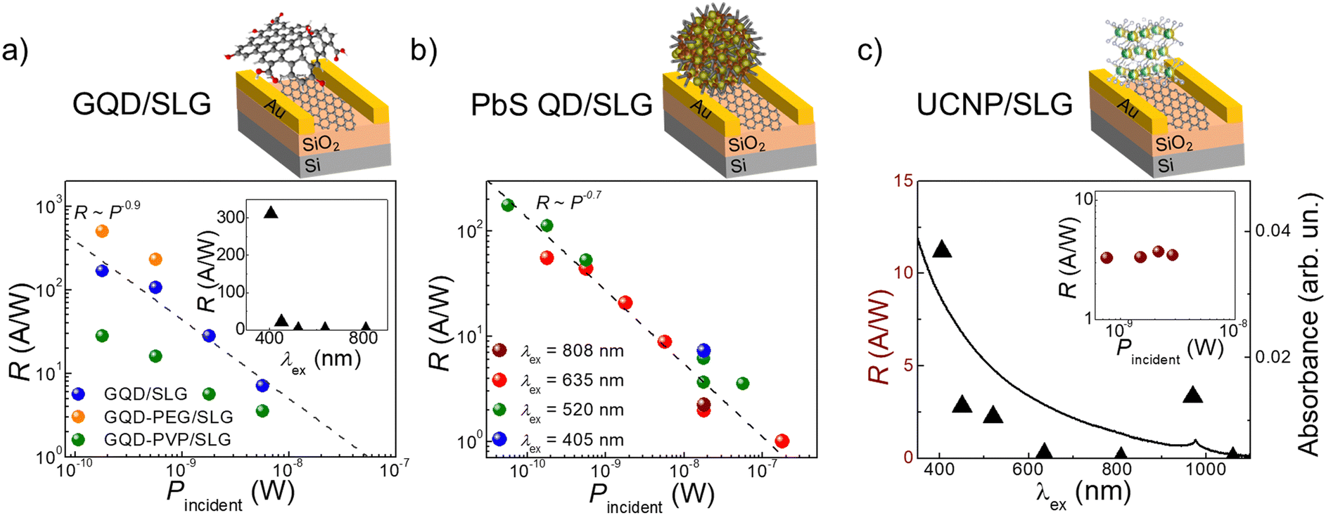 | ||
| Fig. 3 (a) Photoresponsivity, R, as a function of incident light power on the sample, Psample, for the GQD/SLG, GQD-PEG/SLG and GQD-PVP/SLG devices. (Vsd = 2 mV, Vg = 0 V, λex = 405 nm). Inset: R as a function of excitation wavelength, λex, for the GQD/SLG (Vsd = 2 mV, Vg = 0 V, P = 179 W m−2) device. (b) R as a function of Psample for printed PbS QD/SLG device (Vsd = 4 mV, Vg = 0 V) for different λex values (Vsd = 4 mV, Vg = 0 V). (c) R as a function of λex for printed UCNP/SLG device (Vsd = 2 mV, Vg = 0 V, P = 5.7 W m−2), with absorption spectra of UCNPs shown for comparison. Inset: R as a function of Psample for printed UCNP/SLG device (Vsd = 2 mV, Vg = 0 V, λex = 970 nm). | ||
Photoresponsivity across the visible and NIR range was recorded for PbS/SLG from 405 nm to 808 nm (Fig. 3b), with no recorded photoresponse at λex = 1060 nm. These devices reached a photoresponsivity of R ≤ 1.8 × 10² A W−1 and demonstrated recoverable ON/OFF response with τON = 40 s and τOFF ∼300 s (SI2, Fig. S8b, ESI†). All decorated SLG photodetectors had similar power dependence R ∼ P−0.7, which was previously reported for this type of devices prepared using conventional drop-casting or spin-coating methods.28–30 As expected from the absorption profile with a narrow absorption band at 980 nm (FWHM = 15 nm), the UCNPs/SLG device is photosensitive only in this wavelength range (Fig. 3c). Under illumination with λex = 970 nm, the device has R ∼ 3 A W−1 and response times of τON = τOFF = 20 s (SI2, Fig. S8c, ESI†). Interestingly, in these devices, R is independent of illumination power (Fig. 3c, inset). This is an uncommon observation for decorated SLG photodetectors, which might indicate the presence of a photovoltaic effect,31 and merits further detailed studies.
As such, we successfully used our formulated nanoparticle inks to deposit the photosensitive layers onto SLG devices producing photodetectors sensitive across the wavelength range from the UV to the NIR. The difference in photoresponsivity values observed in these devices is affected by a variety of factors, such as nanoparticle size, capping molecules, and dielectric properties of the medium in which nanoparticles are embedded. We envisage that R can be further enhanced by optimising these parameters, to increase the packing density in the layer in immediate proximity to the SLG and pre-select capping material with a lower dielectric constant and shorter chain length.
To demonstrate the versatility of the formulated nanomaterial inks and benefits of geometric design freedom of the inkjet deposition method, we designed and printed a fluorescent UV and NIR sensor, in the shape of a laser-warning sign pattern onto a flexible and transparent PEN substrate, using the NaYbF4:2%Er3+ UCNP, with orange fluorescence, and the CsPbBr3 perovskite NC, with green fluorescence, inks (Fig. 4). We note that for the selected pair of materials, no energy transfer is expected: CsPbBr3 with λ = 514 nm, λabs < 510 nm and NaYbF4:2%Er3+ UCNP with λ = 654 nm, absorption band centred at λabs = 970 nm. Under λex = 365 nm and λex = 980 nm, the sensor exhibited bright green and orange fluorescence, respectively, with well-defined patterns corresponding to the photoluminescence of the perovskite NCs and UCNPs (Fig. 4). Alternative pairs of materials can be selected to enable resonant energy transfer, which could be beneficial for applications, such as energy harvesting, biosensing etc. This work illustrates the opportunities that can be enabled by combining geometric design freedom with novel functional inks developed in this work.
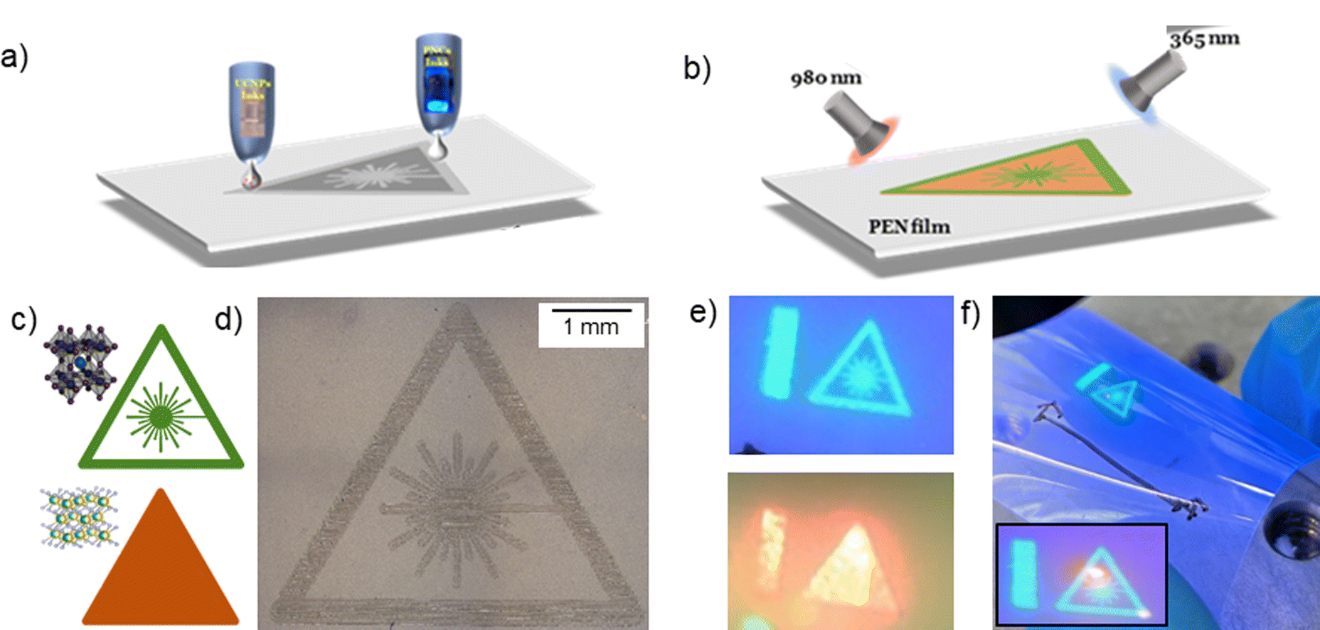 | ||
| Fig. 4 (a) Schematic diagram of inkjet fabrication process of fluorescence sensors containing CsPbBr3 perovskite NCs and NaYbF4:2%Er3+ UCNPs on flexible PEN substrate. (b) Schematic diagram showing the functionality of the sensors: upon 980 nm illumination, the solid triangle displays orange fluoresce from the UCNPs. Under UV illumination the outline and pattern display green fluorescent from the perovskite NCs. (c) Bitmaps used to print fluorescent sensor. The solid triangle of UCNPs was deposited first, and the laser warning pattern of perovskite NCs was printed on top. (d) Optical image of printed laser warning pattern of perovskite NCs with nL = 5 printed layers. (e) Optical images of fluorescence sensor under λex = 365 nm illumination (top) and under λex = 980 nm illumination (bottom). (f) Optical images of fluorescence sensor undergoing bending, under dispersive λex = 365 nm torch illumination with and focussed λex =980 nm laser illumination. | ||
These results demonstrate that inkjet deposition of optically active nanoparticles can provide a route for precise deposition and low-waste sustainable manufacturing, bringing the material advancements achieved in colloidal synthesis to industry relevant processes such as inkjet deposition. Increased availability of functional materials for additive manufacturing could offer exciting opportunities for the development of next generation optoelectronic devices, fluorescence sensing and optical encoding among many others.
The results reported here demonstrate the benefits that can be achieved with inkjet printing of functional materials. Inkjet printing offers high degree of geometric design freedom combined with high precision of drop deposition (∼10 μm), which is not achievable by other solution processing technologies, such as drop-casting and spin coating. The drop-on-demand deposition provides low material waste and multi-material capabilities for fast (20 kHz) and scalable manufacturing of required pattern designs. In addition, compatibility of inkjet deposition with substrates used in traditional silicon-based technologies, offers unique opportunities for functionalisation of devices. For example, multiple SLG devices, typically produced on a single chip, can be selectively and accurately decorated with nanoparticles, for customisable photodetection, as demonstrated in our work.
Experimental methods
Substrates and materials
Prime grade silicon wafers (200 nm SiO2 thickness, PI-KEM) were cleaned by sonicating in acetone for 30 minutes at room temperature followed by washing with IPA and drying with N2. Other substrates, including polyimide (Kapton® HN, DUPONT), borosilicate glass slides (1 mm thickness, Fisher Scientific) and polyethylene terephthalate (PET, 125 μm thickness, GTS Flexible Materials Ltd) were washed with acetone, followed by IPA and dried with N2. Polyethylene naphthalate (PEN, 75 μm thickness, GTS Flexible Materials Ltd) substrates were washed with IPA and dried in N2. High quality CVD grown SLG on Si/SiO2 (285 nm SiO2) field effect transistors (FET) were provided by the Center for Nanotechnology Innovation at NEST, Italy.27Graphene quantum dot, GQD, solution (1 mg mL−1 in water, product number 900560) and graphene ink (2.4 wt% solid content in 85:15 mixture of cyclohexanone/terpineol, product number 793663) were purchased from Sigma Aldrich.
Synthesis of PbS QDs
The following chemicals were used for colloidal synthesis: Alfa Aesar: poly(ethylene glycol); Fisher Chemical: triethylamine, sodium bicarbonate, magnesium sulfate, chloroform, ethyl acetate, hydrochloric acid, dichloromethane, ethanol; Sigma Aldrich: tetrahydrofuran, sodium azide, triphenylphosphine, potassium hydroxide, sodium borohydride, sodium sulfide; Acros Organics: methane sulfonyl chloride, lipoic acid, lead acetate, EDC hydrochloride, 4-(N,N-dimethylamino)-pyridine. The chemical were used as received, without further purifications. Synthesis of NH2-PEG400-DHLA capped PbS QDs with a Pb:S:L ratio of 1:0.3:3 was performed using the method reported previously.21 Briefly, PEG400 (5.00 g, 12.5 mmol), methanesulfonyl chloride (5.8 mL, 75.0 mmol), tetrahydrofuran (THF), triethylamine (TEA), Sodium azide (4.4 g, 68.0 mmol), triphenylphosphine (first addition – 8.58 g, 32.7 mmol; second addition – second time: 3.18 g, 12.1 mmol), 4-(N,N-dimethylamino)-pyridine (0.27 g, 2.1 mmol) and EDC hydrochloride (2.26 g, 2.1 mmol) and lipoic acid (LA, 2.26 g, 11.0 mmol) were reacted through a novel multiple steps ligand exchange routes. N3-PEG400-N3, N3-PEG400-NH2, N3-PEG400-LA and NH2-PEG400-LA were obtained as the reaction intermediates. The final NH2-PEG400-DHLA (0.0864 g, 0.143 mmol) was dissolved in water (10 mL) and the solution was degassed and stirred for 15 min. Pb(OAc)2 (0.1 M, 0.48 mL) was added. The pH was adjusted to 11 with triethylamine (TEA). Na2S (0.15 mL, 0.1 M) was added dropwise to form the nanocrystal under constant stirring. The reaction is performed under N2 flow. The solution of QDs was stored under N2 at 4 °C.
Synthesis of the UCNPs
Yttrium(III) chloride hexahydrate (YCl3·6H2O, 99.9%), ytterbium(III) chloride hexahydrate (YbCl3·6H2O, 99.9%), erbium(III) chloride hydrate (YbCl3·6H2O, 99.9%), oleic acid (OA, 90%) and 1-octadecene (ODE, 90%) were purchased from Sigma Aldrich. Ammonium fluoride (NH4F, ≥98%) and sodium hydroxide (NaOH) were purchased from General Reagent, and hexane, methanol and acetone were purchased from Adams. All chemicals were used as received without further purification. The synthesis of NaYF4:20%Yb3+, 2%Er3+ nanoparticles and NaYbF4:2%Er3+ nanoparticles were performed by thermal coprecipitation method.32 Briefly, for synthesis of NaYF4:20%Yb3+, 2%Er3+ nanoparticles, 970.6 mg YCl3·6H2O (3.12 mmol), 310.0 mg of YbCl3·6H2O (0.80 mmol) and 30.5 mg ErCl3·6H2O (0.08 mmol) solid were combined with 20 mL oleic acid (OA) and 30 mL 1-octadecene (ODE) in a 250 mL three neck round bottom flask, and stirred under Ar atmosphere at temperature T = 120 °C for 1 hour. After cooling to 50 °C, 20 mL NaOH (0.5 M) methanol solution and 32 mL NH4F (0.5 M) methanol solution added dropwise into the flask and stirred for 1 h until the solution became clear. Then the solution was degassed at T = 110 °C for 15 min to remove the residual oxygen, water and methanol. Then the solution was heated to 300 °C for 1 h under continuous string. After cooling to room temperature, the nanoparticles were precipitated by acetone, and collected by centrifugation at 5000 rpm for 5 min and washed three times with hexane/acetone (v/v: 1/4) solution and centrifugation. The final product was dried and collected powder was stored at room temperature in the ambient conditions.Ink formulations
GQD inks were formulated by mixing 1 mg mL−1 GQD solution in water (0.86 mL) with butanol (0.032 mL) and IPA (0.11 mL), and sonicating at room temperature for 30 minutes. By adding 0.86 mg mL−1 of PEG (Mw = 1000), or by adding 0.86 mg mL−1 PVP (Mw = 40000) and sonicating for 30 minutes at room temperature, GQD-PEG and GQD-PVP inks were formulated, respectively. The inks were stored in sealed Dimatix inkjet printing cartridges in ambient conditions. The GQD ink had a viscosity of 1.23 mPa s, a surface tension of 30.9 mN m−1, and density of 1.04 g mL−1. The GQD-PEG ink had a viscosity of 0.75 mPa s, a surface tension of 71.2 mN m−1, and density of 1.06 g mL−1. The GQD-PVP ink had a viscosity of 1.18 mPa s, a surface tension of 32.6 mN m−1, and density of 1.06 g mL−1.
Inks for PbS QDs capped with PEG were made by mixing 1 mg mL−1 of PbS QDs (1 mL) with butanol (0.032 mL) and IPA (0.11 mL). The solution was then sonicated for 30 minutes at room temperature and stored under N2. The ink had a density of 1.01 g cm−3, a viscosity of 0.97 mPa S and a surface tension of 54.5 mN m−1 at room temperature.
UCNP inks were formulated for inkjet printing by dispersing 20 mg mL−1 of UCNPs in 1 mL mixture of hexane, cyclohexanone, and terpineol (1:3:1 v/v) and sonicating for 30 minutes at room temperature. The inks were stable and stored in ambient conditions.
Perovskite nanoparticle inks were formulated by dispersing 5 mg mL−1 CsPbBr3 NCs in a mixture of hexane, cyclohexanone, and terpineol (1:3:1 v/v) and sonicating for 30 minutes at room temperature, and stored at room temperature under N2 atmosphere.10
Inkjet printing process
All nanoparticle inks were deposited using piezo-driven Fujifilm Dimatix DMP-2800 inkjet printer. Printing of all inks was performed with 2.4 pL drop volume Dimatix Samba cartridges. For printing of GQD, GQD-PEG, and GQD-PVP inks the drop spacing of 20 μm and substrate temperature, Tsubstrate = 60 °C were used. A 60 s pause was used between layers to prevent cartridge heating. Printed films were annealed at Tanneal = 100 °C for 30 minutes in air to evaporate the solvents.Printing of PbS QDs was performed with 20 μm drop spacing, Tsubstrate = 60 °C. Printed PbS films were annealed at Tanneal = 100 °C for 30 minutes in air. For printing of UCNP inks, 20 μm drop spacing and Tsubstrate = 60 °C were used. Cleaning cycles were performed with purge for 0.1 s every layer. For post deposition, the UCNPs films were annealed at 250 °C for 1 hour. Perovskite inks were printed under N2 atmosphere with 20 μm drop spacing and Tsubstrate = 60 °C. Cleaning cycles were performed with purge for 0.1 s every layer and films were dried on the print bed for 30 minutes after printing.10
Transmission electron microscopy and energy dispersive X-ray spectroscopy: The transmission electron microscopy (TEM) and energy dispersive X-ray spectroscopy (EDX) were performed on the JEOL 2100F operating at 200 kV equipped with a Gatan K3-IS direct detection camera. And 3 microliters dispersion of sample was drop-casting onto ultrathin carbon support (Agar Scientific ultrathin carbon on lacey amorphous carbon on 400 mesh Cu).
Raman spectroscopy
Micro Raman spectroscopy was performed using a HORIBA LabRAM HR Raman microscope. Spectra were acquired using a 532 nm laser, a 100× objective, and a 200 μm confocal pinhole. To simultaneously scan a range of Raman shifts, rotatable diffraction grating (300 lines per mm) along a path length of 800 mm was employed. Spectra were detected using a Synapse CCD detector (1024 pixels) thermoelectrically cooled to −60 °C. Before spectra collection, the instrument was calibrated using the zero order line and a standard Si(100) reference band at 520.7 cm−1. The spectral resolution is better than 3.8 cm−1 in this configuration.Optical characterisation
Photoluminescence (PL) mapping of GQDs was performed under vacuum using a 405 nm pulsed delta diode laser as the excitation source (pulse rate of 100 MHz with a time-averaged power ∼10 μW and a spot size of ∼2 μm) and a Horiba MicOS optical spectrometer with Si CCD array detector and 50× objective, NA: 0.5, and 150/mm grating. The samples were moved in steps of 20 μm using a motorised Zaber stage attached to the vacuum chamber/cryostat. PL specta of UCNPs was obtained using Edinburgh FLS 1000 with excitation provided by 980 nm continuous laser diode (MDL-III-2W, China).Optical absorbance measurements were conducted with a Cary 3500 UV-Vis spectrophotometer. GQD absorption measurements were obtained by loading 0.01 mg mL−1 solution of GQD inks into quartz cuvettes (Hellma Analytics) and thin film absorption measurements were made by drop-casting onto quartz substrates. UCNP absorption measurements were obtained for 20 mg mL−1 UCNPs inks in Kartell PS 1.5 mL cuvettes.
Electrical measurements
Electrical measurements and photocurrent measurements were performed using Keithley-2400 Source-Meters and Keitheley-2010 multimeters in DC mode. Fixed wavelength excitations were provided by a set of six fibre-coupled diode-pumped solid state DPSS lasers with calibrated output power controlled in the range 1 mW to 30 mW for all output wavelengths (λex = 405, 450, 532, 635, 808, 1060 nm). A 970 nm fibre coupled laser (Thorlabs, M970F3, Pmin = 5.9 mW) with a USB led driver (Thorlabs, upSERIES 1.4) was used as the NIR light source. Responsivity (R) was calculated by R = Ipc/Psample where Ipc is the maximum change in source–drain current (Isd) recorded after one minute of constant illumination and Psample is the total light power incident on the sample. Frequency dependent AC measurements of resistance and capacitance were performed using a Rohde & Schwarz HM8118 Bench LCR Meter.Conclusions
In this work we formulated aqueous and non-polar solvent based inks of colloidal nanoparticles, and demonstrated inkjet printable optically active graphene QDs, PbS QDs, and lanthanide doped upconverting nanoparticles. The developed deposition and optimised post-deposition strategy enabled an exploration of the potential of these inks as photosensitive layers in graphene-based photon detectors with spectral responsivity tuneable by nanoparticle composition and size from the UV to the NIR, and in fluorescent displays using a combination of two nanoparticle layers. Further, these formulations demonstrate a framework by which future breakthroughs in optically active colloidal nanoparticle synthesis can be readily translated into reliable inkjet formulations for further device development. This work is of fundamental and technological interest, as it addresses current challenges by expanding the library of optically active materials for additive manufacturing technologies and provides advantages for the functionalisation of devices compatible with conventional Si-technologies as well as potential applications in flexible and wearable optoelectronics.Author contributions
J. A. and G. R. formulated inks. J. A., W. X., and F. W performed inkjet printing. W. X. synthesised UCNPs and E. W. synthesised PbS QDs. J. A., N. C, and W. X performed electrical measurements. J. A., W. X, and T. J performed optical measurements. F. W., C. T., R. H., W. L., O. M., and L. T. conceptualised the studies. All authors analysed the results, co-wrote the manuscript and approved its submission.Data availability
Data used in the manuscript are available from the corresponding author on request.Conflicts of interest
Authors declare no conflict of interest.Acknowledgements
This work was funded by the Engineering and Physical Sciences Research Council [grant number EP/P031684/1], Quantum Sensors Challenge Program of the National Research Council of Canada and the National Natural Science Foundation of China (52130511, 52375144), China Scholarship Council. The authors acknowledge access to facilities at the Nanoscale and Microscale Research Centre (nmRC) of the University of Nottingham and School of Pharmacy. C. Coletti and V. Miseikis for providing CVD graphene devices; Dr C Zhang for perovskite nanocrystals; Dr G. Rance and Dr M. Fay for Raman and TEM studies, respectively, Mr O. Nelson-Dummett for assistance with absorption measurement, and Dr G. Gordon for useful discussions.References
- S. Singh, Z. H. Khan, M. B. Khan, P. Kumar and P. Kumar, Bull. Mater. Sci., 2022, 45, 81 CrossRef CAS.
- M. A. Triana, E.-L. Hsiang, C. Zhang, Y. Dong and S.-T. Wu, ACS Energy Lett., 2022, 7, 1001–1020 CrossRef CAS.
- J. Zhao, L. Lo, H. Wan, P. Mao, Z. Yu and C. Wang, Adv. Mater., 2021, 33, 2102095 CrossRef CAS PubMed.
- J. Kim, J. Lee, J. Lee, A. Facchetti, T. J. Marks and S. K. Park, Small Methods, 2024, 8, 2300246 CrossRef CAS PubMed.
- B. Cook, M. Gong, D. Ewing, M. Casper, A. Stramel, A. Elliot and J. Wu, ACS Appl. Nano Mater., 2019, 2, 3246–3252 CrossRef CAS.
- J. M. Pietryga, Y. S. Park, J. Lim, A. F. Fidler, W. K. Bae, S. Brovelli and V. I. Klimov, Chem. Rev., 2016, 116, 10513–10622 CrossRef CAS PubMed.
- M. J. Grotevent, C. U. Hail, S. Yakunin, D. N. Dirin, K. Thodkar, G. Borin Barin, P. Guyot-Sionnest, M. Calame, D. Poulikakos, M. V. Kovalenko and I. Shorubalko, Adv. Opt. Mater., 2019, 7, 1900019 CrossRef.
- G. Kara, S. Bolat, K. Sharma, M. J. Grotevent, D. N. Dirin, D. Bachmann, R. Furrer, L. F. Boesel, Y. E. Romanyuk, R. M. Rossi, M. V. Kovalenko, M. Calame and I. Shorubalko, Adv. Mater. Technol., 2023, 8, 2201922 CrossRef CAS.
- M. J. Grotevent, C. U. Hail, S. Yakunin, D. Bachmann, M. Calame, D. Poulikakos, M. V. Kovalenko and I. Shorubalko, Adv. Sci., 2021, 8, 2003360 CrossRef CAS PubMed.
- J. S. Austin, N. D. Cottam, C. Zhang, F. Wang, J. H. Gosling, O. Nelson-Dummet, T. S. S. James, P. H. Beton, G. F. Trindade, Y. Zhou, C. J. Tuck, R. Hague, O. Makarovsky and L. Turyanska, Nanoscale, 2022, 15, 2134–2142 RSC.
- A. M. Alamri, S. Leung, M. Vaseem, A. Shamim and J. H. He, IEEE Trans. Electron Devices, 2019, 66, 2657–2661 CAS.
- H. Lee, W. Harden-Chaters, S. D. Han, S. Zhan, B. Li, S. Y. Bang, H. W. Choi, S. Lee, B. Hou, L. G. Occhipinti and J. M. Kim, ACS Appl. Nano Mater., 2020, 3, 4454–4464 CrossRef CAS.
- E. Schlake and N. Kandadai, IEEE J. Flex. Electron., 2024, 1 Search PubMed.
- P. Peng, N. Wu, L. Ye, F. Jiang, W. Feng, F. Li, Y. Liu and M. Hong, ACS Nano, 2020, 14, 16672–16680 CrossRef CAS PubMed.
- B. Chen and F. Wang, Trends Chem., 2020, 2, 427–439 CrossRef CAS.
- A. Schroter, S. Märkl, N. Weitzel and T. Hirsch, Adv. Funct. Mater., 2022, 32, 2113065 CrossRef CAS.
- J. Xu, J. Zhou, Y. Chen, P. Yang and J. Lin, Coord. Chem. Rev., 2020, 415 Search PubMed.
- F. Wang and X. Liu, J. Am. Chem. Soc., 2008, 130, 5642–5643 CrossRef CAS PubMed.
- Y. Liu and D. Y. Kim, Chem. Commun., 2015, 51, 4176–4179 RSC.
- A. Bastola, Y. He, J. Im, G. Rivers, F. Wang, R. Worsley, J. S. Austin, O. Nelson-Dummett, R. D. Wildman, R. Hague, C. J. Tuck and L. Turyanska, Mater. Today Electron., 2023, 6, 100058 CrossRef.
- F. Zamberlan, L. Turyanska, A. Patanè, Z. Liu, H. E. L. Williams, M. W. Fay, P. A. Clarke, Y. Imamura, T. Jin, T. D. Bradshaw, N. R. Thomas and A. M. Grabowska, J. Mater. Chem. B, 2018, 6, 550–555 RSC.
- X. Yu, R. Xing, Z. Peng, Y. Lin, Z. Du, J. Ding, L. Wang and Y. Han, Chin. Chem. Lett., 2019, 30, 135–138 CrossRef CAS.
- W. K. Hsiao, G. D. Martin and I. M. Hutchings, Langmuir, 2014, 30, 12447–12455 CrossRef CAS PubMed.
- W. Xiao, J. Chen, F. Wang, W. Luan, Y. Wu and L. Turyanska, Adv. Opt. Mater., 2024, 2303132 CrossRef CAS.
- N. D. Cottam, C. Zhang, L. Turyanska, L. Eaves, Z. Kudrynskyi, E. E. Vdovin, A. Patane and O. Makarovsky, ACS Appl. Electron. Mater., 2020, 2, 147–154 CrossRef CAS.
- N. D. Cottam, J. S. Austin, C. Zhang, A. Patanè, W. Escoffier, M. Goiran, M. Pierre, C. Coletti, V. Mišeikis, L. Turyanska and O. Makarovsky, Adv. Electron. Mater., 2023, 9, 2200995 CrossRef CAS.
- S. Pezzini, V. Mišeikis, S. Pace, F. Rossella, K. Watanabe, T. Taniguchi and C. Coletti, 2D Mater., 2020, 7, 041003 CrossRef CAS.
- L. Turyanska, O. Makarovsky, S. A. Svatek, P. H. Beton, C. J. Mellor, A. Patanè, L. Eaves, N. R. Thomas, M. W. Fay, A. J. Marsden and N. R. Wilson, Adv. Electron. Mater., 2015, 1, 1500062 CrossRef.
- S. H. Cheng, T. M. Weng, M. L. Lu, W. C. Tan, J. Y. Chen and Y. F. Chen, Sci. Rep., 2013, 3, 2694 CrossRef PubMed.
- M. Kataria, K. Yadav, G. Haider, Y. M. Liao, Y. R. Liou, S. Y. Cai, H. I. Lin, Y. H. Chen, C. R. Paul Inbaraj, K. P. Bera, H. M. Lee, Y. T. Chen, W. H. Wang and Y. F. Chen, ACS Photonics, 2018, 5, 2336–2347 CrossRef CAS.
- H. Yao, G. Peng, Z. Li, G. Zhu, W. Li, Z. Ci, W. Lan, H. Jia, B. Dong and Z. Jin, J. Energy Chem., 2022, 65, 524–531 CrossRef CAS.
- F. Wang, R. Deng and X. Liu, Nat. Protoc., 2014, 9, 1634–1644 CrossRef CAS PubMed.
Footnote |
| † Electronic supplementary information (ESI) available. See DOI: https://doi.org/10.1039/d4tc01917b |
| This journal is © The Royal Society of Chemistry 2024 |