
Regulating the microscopic structure of solutions to synthesize centimeter-sized low-dimensional CsmSbnClm+3n perovskite single crystals for visible-blind ultraviolet photodetectors†
Wenzhen
Wang
 abd,
Shanhu
Xu
a,
Ziyi
Lai
a,
Xiaoxi
Feng
a,
Huanzhen
Qi
a,
Qiutao
Pan
a,
Zichen
Yang
c,
Jiaxing
Kang
c,
Yue
Li
c,
Xin
Shu
c,
Zifa
Zhang
c,
Yan
Zhu
d,
Jiaxin
Bai
e,
Feng
Hong
c,
Juan
Qin
b,
Run
Xu
*ab,
Ying
He
c,
Fei
Xu
c and
Linjun
Wang
abc
abd,
Shanhu
Xu
a,
Ziyi
Lai
a,
Xiaoxi
Feng
a,
Huanzhen
Qi
a,
Qiutao
Pan
a,
Zichen
Yang
c,
Jiaxing
Kang
c,
Yue
Li
c,
Xin
Shu
c,
Zifa
Zhang
c,
Yan
Zhu
d,
Jiaxin
Bai
e,
Feng
Hong
c,
Juan
Qin
b,
Run
Xu
*ab,
Ying
He
c,
Fei
Xu
c and
Linjun
Wang
abc
aSchool of Materials Science and Engineering, Shanghai University, 333 Nanchen Road, Shanghai 200444, China. E-mail: runxu@shu.edu.cn
bZhejiang Institute of Advanced Materials, SHU, 1588 Huaxiang Street, Jiashan 314113, China
cDepartment of Physics, College of Sciences, Shanghai University, 99 Shangda Road, Shanghai 200444, China
dShanghai Technical Institute of Electronics & Information, 3098 Wahong Road, Shanghai 201411, China
eHebei Institute of Pure Iron Materials and Application Industry Technology, Handan 056300, China
First published on 27th November 2023
Abstract
Chlorine-based all-inorganic lead-free halide perovskites exhibit excellent properties in visible-blind ultraviolet detectors. However, the quality and size of these solution-grown single crystals are still far from meeting commercial standards due to their low solubility, and a fundamental understanding of the underlying causes of low solubility is still lacking. Herein, the effects of the microscopic structure of solutions on the solubility have been systematically investigated, and it has been demonstrated that a hybrid solvent consisting of dimethyl sulfoxide and hydrochloric acid can significantly improve the solubility of the raw materials of CsmSbnClm+3n (SbCl3 and CsCl). Centimeter-sized high-quality α-Cs3Sb2Cl9 and Cs5Sb2Cl11 single crystals are grown by the effective hybrid solvent. The low dark current density (91 pA cm−2), excellent wavelength selectivity (R360/R480 = 150), and fast response speed (tr = 21.7 ms, td = 104.4 ms) of the photodetector based on the Au/α-Cs3Sb2Cl9/Au structure powerfully demonstrate the great potential of CsmSbnClm+3n in ultraviolet applications. Furthermore, the method of using hybrid solvents to increase solubility can be extended to the growth of all inorganic chloride perovskite single crystals, thereby driving the exploration of their future optoelectronic applications.
Introduction
Compared to polycrystalline films, nanocrystals, and nanowires, high-quality metal halide perovskite (PVK) single crystals with lower trap density may be considered to be the most attractive emerging materials for detection applications.1 Solution growth has become a mainstream method for the growth of PVK single crystals due to the low cost of the equipment, the simplicity of operation and the ease of growth into crystals with good homogeneity and complete shape.2,3 The choice of solvent, solubility and temperature are critical factors affecting the growth rate and quality of single crystals, with solubility being particularly crucial. Excessive solute solubility makes it challenging to precipitate crystals from the solution, while low solubility restricts the size and growth rate of the crystals. Ideally, the growing material should have moderate solubility in the solvent, with a sufficient solubility gradient. Compared to organic–inorganic hybrid PVKs, all-inorganic perovskites are more stable and less prone to decomposition, thus making it difficult for them to grow into large sized crystals in solution due to the relatively low solubility.4 In particular, chlorine-based inorganic perovskites have a larger bandgap than iodine- and bromine-based inorganic PVK, making them more suitable for visible-blind ultraviolet5,6 (UV) detector applications. Fang et al. have demonstrated that it is difficult to fabricate high-quality wide bandgap CsPbCl3 because of the poor solubility of CsCl and PbCl2 in dimethylsulfoxide (DMSO).7 Actually, the UV detectors prepared by chlorine-based inorganic perovskite single crystals have been rarely reported due to their low solubilities, which limit the quality and size of solution-grown single crystals and seriously hinder their commercial applications. Therefore, understanding the reasons for the low solubility of chlorine-based inorganic perovskites and exploring effective ways to increase their solubility are critical priorities for improving single crystal growth. In this work, we chose the environmentally friendly CsmSbnClm+3n (CSC) perovskite as a typical material to investigate the dissolution conditions in single crystal growth, as it has the lowest solubility among the reported chlorine-based inorganic PVKs.CsmSbnClm+3n is a low-dimensional perovskite structure material derived from the traditional three-dimensional (3D) ABX3 (A = CH3NH3+, CH(NH2)2+, Cs+; B = Pb2+, Sn2+; X = I−, Br−, Cl−) perovskite, which overcomes the issues of phase transformation and instability of 3D PVKs.8 Sb-based PVKs have the same lone-pair ns2 outermost electronic configuration of the Sb3+ element as for Pb2+, resulting in similar photoelectric properties to those of Pb-based PVK materials.9 The history of the synthesis of trigonal and orthorhombic Cs3Sb2Cl9 could be backtracked to 1970,10 while most reports have focused on the preparation of nanowires,11 nanocrystals,12 and thin films.13 Pradhan and co-workers synthesized Cs3Sb2Cl9 PVK nanowires with lengths up to several microns by a colloidal route and fabricated a Cs3Sb2Cl9 nanowire-based photodetector with a detectivity of 1.25 × 10⁶ Jones, as well as the rise time and decay time of 0.13 s and 0.23 s, respectively.11 There are still no relevant reports on the growth of centimeter-sized Cs3Sb2Cl9 single crystals and the fabrication of the corresponding UV detector. As mentioned above, the main challenge comes from the fact that the raw materials of CSC (CsCl and SbCl3) are difficult to dissolve in a conventional single solvent simultaneously, and the solubility of the precursor solution is too low to grow CSC single crystals.13 The solution-based growth of single crystals depends strongly on the precursor solvent, which can be divided into aqueous acid solvents (e.g., hydroiodic acid, hydrobromic acid, and hydrochloric acid) and organic solvents (e.g., N,N-dimethylformamide (DMF), γ-butyrolactone (GBL), DMSO, N-methyl pyrrolidone (NMP), acetone, ethanol, isopropanol, etc.). Unfortunately, neither of the aforementioned solvent types can dissolve the Cs3Sb2Cl9 precursor at high concentrations. Among only a few reports, Cs3Sb2Cl9 is obtained by cooling or evaporating a mixed solution of CsCl and SbCl310,14 or Sb2O315,16 dissolved in dilute hydrochloric acid, while the solubility is still insufficient to grow large-sized Cs3Sb2Cl9 single crystals. Therefore, it is imperative to improve the solubility of the precursor solution and grow high-quality centimeter-sized Cs3Sb2Cl9 single crystals for application in ultraviolet photodetectors.
In this work, we have successfully prepared clear PVK precursor solutions using hybrid solvents with enhanced solubility due to the presence of both SbClx3−x colloids and Cs+ ions in the solution. By controlling the molar ratio of the raw materials, the centimeter-sized all-inorganic α-Cs3Sb2Cl9 and Cs5Sb2Cl11 perovskite single crystals were grown through the gradient cooling temperature crystallization method (GCTCM). The structural characterization and optical properties of the prepared CSC single crystals have been systematically investigated, confirming that CSC is an ideal material for photodetectors sensing UV light radiation. The visible-blind ultraviolet photodetectors based on CSC single crystals were fabricated, demonstrating good wavelength selectivity and fast response speed.
Experimental
Materials and chemicals
Cesium chloride (CsCl, 99.9%, Xi'an Polymer Light Technology Corp), Antimony(III) chloride (SbCl3, 99.99%, Aladdin), dimethylsulfoxide (DMSO, 99.9%, Aladdin), ethyl alcohol (GR, Sinopharm), isopropanol (AR, Sinopharm), N-methyl pyrrolidone (NMP, 99.9%, Aladdin), N,N-dimethylformamide (DMF, 99.9%, Aladdin), γ-butyrolactone (GBL, 99%, TCI), hydrochloric acid (HCl, 37 wt%, Sinopharm).Perovskite precursor solution preparation
It was obvious that the inherent concentration of dilute hydrochloric acid and the volume ratio of hydrochloric acid to DMSO directly affect the concentration of the precursor solution, therefore, their effects on the solubility were investigated. The solubility of the mixed powders of CsCl and SbCl3 exhibited an increasing-then-decreasing trend as the inherent concentration of hydrochloric acid decreased, while maintaining the fixed volume ratio of DMSO to dilute hydrochloric acid (4![[thin space (1/6-em)]](https://www.rsc.org/images/entities/char_2009.gif) :1). It reached its maximum value at a concentration of 8 wt%, as shown in Fig. S1 in the ESI.† Subsequently, the inherent concentration of hydrochloric acid in the hybrid solvent was set to 8 wt%, and the optimal solubility of CsCl and SbCl3 mixed powders was attained at a DMSO to HCl volume ratio of 3:1. This ratio was found to be the most effective after considering alternative ratios of 2:1, 3:1, 4:1, and 1:4.
:1). It reached its maximum value at a concentration of 8 wt%, as shown in Fig. S1 in the ESI.† Subsequently, the inherent concentration of hydrochloric acid in the hybrid solvent was set to 8 wt%, and the optimal solubility of CsCl and SbCl3 mixed powders was attained at a DMSO to HCl volume ratio of 3:1. This ratio was found to be the most effective after considering alternative ratios of 2:1, 3:1, 4:1, and 1:4.
As a result, the DMSO:HCl (8 wt%) mixture with a volume ratio of 3:1 was finally selected as the hybrid solvent for the preparation of the precursor solution. Then CsCl and SbCl3 are dissolved in the as prepared 3DMSO:HCl (8 wt%) solvent mixture with molar ratios of 3:2 and 5:2, respectively. The mixture solution was stirred at 90 °C overnight.
Single crystal growth
CSC single crystals were prepared via the controlled gradient cooling temperature crystallization method. The as-prepared perovskite precursor solution was maintained at 95 °C, then the temperature was decreased by 5 °C every 6 hours to 80 °C, and then lowered by 4 °C every 12 hours to 60 °C, and subsequently cooled at a rate of 2 °C day−1 until 54 °C, at which stage single crystals began to appear, and then continuously cooled at a rate of 2 °C day−1 to allow the single crystals to slowly grow. Centimeter-sized single crystals of pale-yellow color α-Cs3Sb2Cl9 and colorless Cs5Sb2Cl11 were obtained after 14 days.Characterization
Powder XRD patterns were recorded using an X'Pert3 powder X-ray diffractometer (Malvern Panalytical) equipped with a Cu tube operated at 40 kV and 30 mA. The X-ray intensity data of CSC single crystals were measured on a Bruker D8 VENTURE DUO PHOTON III Bruker APEX-II CCD system equipped with an Incoatec Ius 3.0 Microfocus sealed tube (Mo Kα, λ = 0.71073 Å) and a Helios MX Multilayer Optical monochromator. The Rietveld refinements were performed by using a Bruker SHELXTL software package. The high-resolution X-ray rocking curve (XRC) was obtained using an Empyrean multifunctional X-ray diffractometer (Malvern Panalytical), with a Cu Kα1 line operated at V = 40 kV and I = 20 mA. The Raman spectroscopy studies were performed by using a Horiba Jobin Yvon LabRAM HR800 Raman spectrometer with an ultraviolet pulsed 355 nm laser beam as the excitation source. XRF spectra were measured with MXF-2400 multi-channel X-ray fluorescence spectrometer (Shimadzu). XPS spectra were measured using an Escalab 250Xi photoelectron spectrometer (Thermo Scientific). The UV-Vis absorbance and transmittance spectra were recorded at room temperature using a PerkinElmer Lambda 950 UV–vis–NIR spectrophotometer with a scan speed 300 nm min−1 and a slit width quantitative 5 nm in a wavelength range of 200–900 nm at room temperature. A highly refined barium sulfate (BaSO4) plate was used as the reference (100% reflectance). The temperature-dependent steady-state photoluminescence (PL) spectra were recorded on an RF-5301pc spectrofluorometer (Shimadzu) with the operating temperature ranging from 10 K to 275 K using the 266 nm laser beam. Time-resolved emission data were collected at room temperature using a FluoroMax spectrofluorometer (Horiba). The dynamics of emission decay was monitored by using a FluoroMax spectrofluorometer with time-correlated single-photon counting capability (4096 channels) with data collection for 10000 counts.
Theoretical calculations
Defect calculations were performed in the framework of DFT using the projector-augmented wave (PAW) method, and the screened hybrid Heyd–Scuseria–Ernzerhof (HSE) functionals, as implemented in the Vienna Ab initio simulation package (VASP).17 The plane-wave cutoff energy was set to 450.0 eV. The van der Waals (vdWs) dispersion correction was applied and described by the DFT-D3 correction.18 The employed primitive cell and Γ-centered k-mesh are 7 × 7 × 5 for α-Cs3Sb2Cl9 and 4 × 4 × 4 for Cs5Sb2Cl11, respectively. The lattice parameters and atomic positions of all the structures were relaxed until the Hellmann–Feynman forces on them were smaller than 0.01 eV Å−1. The calculated lattice constants are a = b = 7.7966 Å, c = 9.5322 Å for α-Cs3Sb2Cl9, and a = 13.6997 Å, b = 12.8955 Å, and c = 14.7419 Å for Cs5Sb2Cl11, respectively.Device fabrication and detection performance characterization
To prepare CSC photodetectors, these polished single crystals were sandwiched between the rectangular electrodes (2 mm × 2 mm) Au (50 nm), and then deposited on both sides of the single crystal using a thermal evaporator. The current–voltage (I−V) curves of photodetectors in the dark and under different irradiation were measured (2400 Series source meter, Keithley Instruments Inc.) by using a 266 nm laser beam with the bias voltage in the range from −30 V to 30 V. The time-dependent photoresponse signal was recorded using a 1 GHz digital oscilloscope with a Keithley 428 current amplifier. The spectral responsivity was measured using a monochromator combined with an optical chopper and a lock-in amplifier. The light intensity was calibrated by a UV enhanced silicon photodetector in the wavelength range of 200–700 nm. All the optoelectronic properties were measured under the atmospheric environment.Results and discussion
Solvent for the preparation of the precursor solution
In the process of growing single crystals by the solution method, the preparation of the precursor solution is of crucial importance. According to the “like dissolves like” rule, solutes composed of polar molecules are easily soluble in polar solvents and difficult to dissolve in nonpolar solvents. Therefore, polar solvents should be employed to dissolve SbCl3, while CsCl, an ionic crystal, can be ionized in polar solvents to produce charged anions and cations. Since solvent molecules in polar solvents have positive and negative polarity, there is a strong attraction between solvent molecules and solute ions. This attraction allows the anions and cations to overcome the Coulomb attraction between each other and diffuse into the solvent. Therefore, CsCl can be dissolved in solvents with large polarity. In order to obtain stable precursor solutions with high concentrations, a variety of polar solvents are used in the experiment for the dissolution of the CsCl, SbCl3, CsCl and SbCl3 mixture with a mole ratio of 3:2, and Cs3Sb2Cl9 powder synthesized as reported, including DMSO, DMF, NMP, GBL, hydrochloric acid, ethanol, isopropanol, and deionized water, etc. As listed in Table S1 in the ESI,† CsCl is highly soluble in deionized water and hydrochloric acid, but hardly dissolves in organic solvents due to the different polarities of these solvents. The order of polarity of the solvents is as follows, water > DMSO > NMP > DMF > ethanol > isopropanol > GBL, the solubility of CsCl decreases with the decrease of solvent polarity. Also note that SbCl3 with more covalent bonds is easily soluble in both organic solvents and hydrochloric acid at high concentrations, while it is difficult to dissolve in deionized water and undergoes a hydrolysis reaction as indicated by the following eqn (1),| SbCl3 + H2O = SbOCl↓ + HCl. | (1) |
Since either CsCl or SbCl3 is easily soluble in hydrochloric acid, it could be supposed that the mixture of CsCl and SbCl3 can dissolve well in this solution. Unfortunately, the mixture of CsCl and SbCl3, as well as Cs3Sb2Cl9 powder, are all much more difficult to dissolve in hydrochloric acid, and organic solvents as well (Table S1† and Fig. 1a). It is noteworthy that the solubility of CsCl and SbCl3 mixed powders in DMSO is the lowest, only 0.019 g ml−1, which can give rise to the difficulty of dissolving CsCl in DMSO (0.005 g ml−1). Therefore, the low solubility of the Cs3Sb2Cl9 precursor solution by using a single solvent makes the growth of a large single crystal almost impossible.
 | ||
| Fig. 1 Dissolution conditions in different solvents. (a) Solubilities of CsCl, SbCl3, CsCl and SbCl3 mixed powders in different solvents at 75 °C. For a clearer presentation, the solubility values of CsCl are multiplied by 10, and that of CsCl + SbCl3 mixed powders are multiplied by 100. (b) Solubility curve and concentration at different temperatures. (c) Raman spectra of the upper clear layers of the well-stirred solutions prepared by CsCl, SbCl3, and CsCl and SbCl3 mixed powders. Black: pure solvent, red: SbCl3 solution, blue: CsCl solution, green: solution prepared using CsCl and SbCl3 mixed powders. (d) Schematic diagram of the precursor solution state. | ||
Then, several hybrid solvents were investigated, and it was found that the hybrid solvent mixed with DMSO and hydrochloric acid can improve the solubility of Cs3Sb2Cl9, as shown in Fig. 1a, b, and Fig. S1.† The solubility of the mixed powders in the hybrid solvent of DMSO and hydrochloric acid (8 wt%) is 0.135 g ml−1, which is more than 6 times higher than that in DMSO and almost 2.5 times as high as that in hydrochloric acid (8 wt%).
In order to reveal the reason for the increase in solubility in the hybrid solvent, the existing modes of solutes in each solvent were investigated. As shown in Fig. S2,† the typical Tyndall effect was observed for SbCl3 in all three solvents, indicating that SbCl3 could be coordinated in the solvent19 and form various coordination products of SbClx3−x, such as SbCl2+, SbCl2+, SbCl3, SbCl4−, SbCl52−, and SbCl63−, similar to that reported for PbI2.20 In contrast, after the addition of CsCl, the intensity of the Tyndall effect has become lower, indicating that the addition of CsCl disrupts part of the SbClx3−x framework and reduces the number of colloids, especially in hydrochloric acid, where the Tyndall effect is no longer observed, suggesting that colloids are completely decomposed by the combined action of H+ and Cs+,21,22 and the solute exists in the ionic state in hydrochloric acid.
In addition, the Raman spectra of the prepared well-stirred solutions can confirm the above results about the type of solute particles present in solutions. As shown in Fig. 1c, the Raman peak positions of CsCl in solution basically overlap with those of the pure solvent, regardless of whether it is dissolved in a single solvent or a hybrid solvent, since CsCl is an ionic crystal that presents in the solvent as Cs+ and Cl− ions. In contrast, the Raman spectra of SbCl3 in all solutions show a noticeable peak shape variation at the region of 230, 276, and 339 cm−1 shift, which should be assigned to the Sb–Cl stretching vibrational bands.23,24 It is worth noting that the peak position and shape of the Raman spectra of the CsCl and SbCl3 mixed powders in DMSO and DMSO:HCl (8 wt%) are consistent with that of SbCl3 in the corresponding solvent under the same SbCl3 mole concentration, with only a slight decrease in the intensity of the Sb–Cl peak, confirming that the addition of CsCl causes the partial decomposition of the SbClx3−x colloids and a decrease in the number of colloids. In comparison, the peak positions of the CsCl and SbCl3 mixed powders in hydrochloric acid basically overlap with that of the hydrochloric acid itself, but are very different from that of SbCl3 dissolved in hydrochloric acid, with no characteristic Sb–Cl peak, indicating the absence of colloids, which is consistent with the results of the Tyndall effect.
A schematic diagram shown in Fig. 1d can then demonstrate the evolution of the type of solute particles present in precursor solutions from a single solvent to a hybrid solvent, as evidenced by the Raman spectra and the Tydnall effect described above. As shown in Fig. 1c, the solubility of either CsCl or SbCl3 powders alone is high in hydrochloric acid (8 wt%), while the solubility decreases substantially once these two powders are mixed. This is because the addition of Cs+ into SbCl3 solution can decompose a large number of SbClx3−x frameworks into ions, so that the ion concentration reaches supersaturation, thus forming CSC precipitates. When DMSO is added to the hydrochloric acid precursor, a small amount of SbClx3−x colloids could exist stably in the hybrid solvent, leading to the improvement of solubility. This result is consistent with the report by Snaith et al.,21 from which it can also be deduced that the presence of colloids can lead to the improvement of the solute solubility. On the other hand, CsCl is almost completely insoluble in DMSO, while the addition of hydrochloric acid into DMSO can raise the solubility of CsCl substantially (0.088 g ml−1), thus greatly improving the solubility of the mixed powders in the hybrid solvent of DMSO and hydrochloric acid. These results strongly suggest that the hybrid solvent of DMSO and hydrochloric acid is more suitable as the precursor solution to grow large-sized CSC single crystals.
The saturated solubility curve of CSC in this hybrid solvent measured at different temperatures is shown in Fig. 1b, which increases with the increase of temperature, showing the positive temperature crystallization characteristics of CSC. The solubility curve and the super-solubility curve divide the diagram into three regions, i.e., the unsaturated, supersaturated, and metastable regions. It is the metastable region that is much more suitable for large crystal growth, in agreement with CH3NH3PbI3.25 In this study, pale-yellow color single crystals with the size of 10 × 8 × 2 mm3 and colorless single crystals with the size of 11 × 9 × 4 mm3 were prepared via the controlled gradient cooling temperature crystallization method using the CsCl and SbCl3 mixture in stoichiometric ratios of 3:2 and 5:2, respectively, for details see the Materials and methods section. Different cooling rates are used to step down the temperature at different stages of crystal growth. At the initial stage, the temperature was lowered at a fast rate (5 °C every 6 hours) to near the solubility curve, then at a slow rate (4 °C every 12 hours) in the metastable region to near the super-solubility curve, and finally at a very low rate (2 °C day−1) before and after the precipitation of the seed crystals, so that the crystals were grown slowly in the metastable region to grow large single crystals.
Structural characterization of Cs3Sb2Cl9 and Cs5Sb2Cl11
These as-grown single crystals were characterized using single-crystal X-ray diffraction (SCXRD) and double-axis high-resolution X-ray rocking curve (XRC) for the study of the structure, while powders milled from the crystals were characterized by powder X-ray diffraction (PXRD) technology. The PXRD results shown in Fig. 2a demonstrate that the as-obtained pale-yellow color single crystals are in perfect agreement with the theoretical data of α-Cs3Sb2Cl9, which possesses a crystal structure with the trigonal space group of P321. The θ–2θ X-ray measurement for the surface growth plane of the crystal shows only five sharp and narrow diffraction peaks along the (001) plane, indicating the good crystallinity of α-Cs3Sb2Cl9 single crystals. As shown in Fig. 2b and Fig. S3,† the crystal structure of the 2D layered α-Cs3Sb2Cl9 is derived from the hypothetical perovskite compound CsSbCl3 (i.e., Cs3Sb3Cl9) by removing every third Sb layer along 〈111〉 to achieve correct charge balance.26,27 The trigonal unit cell is built of isolated layers formed by six-membered rings of SbCl6 octahedra pointed up and down alternatively with respect to the plane of common atoms Cl, and the monovalent cesium cations are located in the large cavities formed in the center of those rings and below or above each SbCl6 octahedra thus filling all empty folds within the layer.28 The unit cell parameters, a = b = 7.809 Å, c = 9.574 Å, α = β = 90°, γ = 120°, are presented in Table S2 in the ESI.† As a result of distortion, two different bond lengths for the Sb–Cl bonds are observed in the SbCl6 octahedron, which for Sb–Cl1 and Sb–Cl2 are calculated to be 2.847 Å and 2.528 Å, respectively.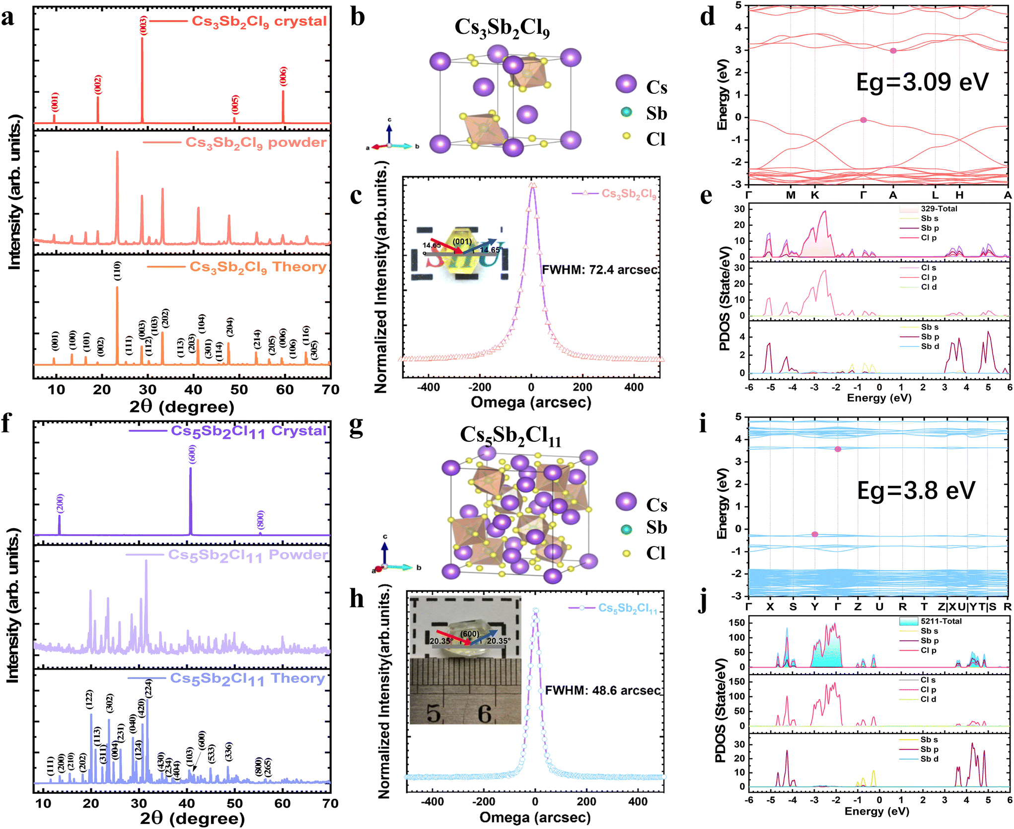 | ||
| Fig. 2 Structural Characterization of Cs3Sb2Cl9 and Cs5Sb2Cl11. (a) and (f) X-ray diffraction curve of calculated data, ground powder from large CSC single crystals, and as-grown single crystals. (b) and (g) Crystal structure of the CSC unit cell. (c) and (h) X-ray rocking curves of CSC single crystals. Insets: photographs of the as-grown crystals. (d) and (i) The electronic band structures of CSC and the band edge positions are indicated by the red and blue dots, highlighting the nature of indirect band gaps in these materials. (e) and (j) Electronic DOS for CSC crystals. (a)–(e) Cs3Sb2Cl9. (f)–(j) Cs5Sb2Cl11. | ||
The structure of the colorless single crystal was solved and refined using the Bruker SHELXTL Software Package, the SCXRD data are shown in Fig. 2f, fitting the space group Pbca, with Z = 4 for the formula unit, Cs5Sb2Cl11, which are also consistent with the PXRD measurements. The X-ray 2θ scan on the growth plane of Cs5Sb2Cl11 (CCDC 2307326) shows only (200), (600), and (800) diffraction peaks, suggesting good single crystalline quality, as do the grown α-Cs3Sb2Cl9 crystals. The XRD studies reveal that Cs5Sb2Cl11 crystallizes at room temperature in orthorhombic symmetry with the following lattice constants: a = 13.1584 (3) Å, b = 12.4187 (4) Å, c = 14.4150 (4) Å, volume = 2355.56 (11) Å3, as shown in Fig. 2g and Tables S3–S5 in the ESI.† The Cs5Sb2Cl11 crystal is built up of cesium cations and discrete [Sb2Cl11]5− groups, which represent a new type of halide complex, such as (CH3NH3)5Bi2X11 type crystals.29–31 [Sb2Cl11]5− consists of two SbCl6 octahedra joined via one chlorine bridge, in which the bridging Sb–Cl (1) bond is longer (2.8920 Å) and the Sb–Cl (4) bond along the direction of the Sb–Cl (1) bond is shorter (2.4592 Å) than the other four terminal bonds (between 2.5629 and 2.7057 Å), and most of these bond angles are about 90 or 180°.32
The phase purity and crystallinity of the as-grown crystals were confirmed by XRD scans of the growth plane and corresponding power, and the crystalline quality was evaluated by XRC. We performed the XRC of (003) diffraction for as-grown Cs3Sb2Cl9 crystals and (600) diffraction for Cs5Sb2Cl11 crystals, respectively, as illustrated in Fig. 2c and h. The full width at half maximum (FWHM) of the XRC peak was found to be 72.4 arcsec for as-grown Cs3Sb2Cl9 crystals, and 48.6 arcsec for Cs5Sb2Cl11 crystals, demonstrating good crystalline quality comparable to conventional Pb-based halide PVK crystals.25,33
To explore the elemental compositions of the crystals, they were measured by X-ray fluorescence (XRF) techniques. As shown in Fig. S4,† the XRF data show an atomic ratio of Cs/Sb/Cl ≈ 2.9:2:8.9, which matches closely to the Cs3Sb2Cl9 chemical composition. As for the XRF data of as-grown Cs5Sb2Cl11 crystals, the atomic ratio of Cs/Sb/Cl is about 5:2.1:12.7, close to the stoichiometric ratio of Cs5Sb2Cl11, but there is a slight excess of SbCl3 on the crystal surface. Further evidence of component analysis shows the characteristic peaks for Cs, Sb, and Cl via X-ray photoelectron spectroscopy (XPS) measurements (Fig. S5†). XPS spectra confirm the presence of Cs+, Sb3+ and Cl− states within the CSC crystals, for example, the Sb 3d3/2 and 3d5/2 doublet peak with binding energies of 539.7 and 530.5 eV are corresponding to the Sb3+ state.34 Note that the calculated atomic ratio of Cs/Sb/Cl for the Cs5Sb2Cl11 crystal is around 5:2.9:12.5, which is similar to the result of XRF. Excess SbCl3 may be resulting from the etching process35 during the removal of the crystals from the growth solution, and the same phenomenon was found for CH3NH3PbI3.
Since the band gap is the key quantity for selecting photodetector materials, it is hence calculated using the Heyd–Scuseria–Ernzerhof (HSE) hybrid functional,36–38 with full details provided in the Experimental section, as the hybrid density functional usually gives the accurate fundamental band gaps for most semiconductors. As illustrated in Fig. 2d and i, band edge positions in band structures are indicated by the red and blue dots, highlighting the nature of indirect band gaps of CSC materials. The indirect bandgap of Cs3Sb2Cl9 is 3.09 eV, while that of Cs5Sb2Cl11 is 3.80 eV, both of which are well suited for UV detectors. The projected density of states (PDOS) for CSC are shown in Fig. 2e and j. The semi core state of Cs p states forms a narrow band located at a deep energy of −8 eV, and have almost no contribution to the valence band maximum (VBM) and conduction band minimum (CBM), the same as other CsBX3 PVKs.36 With regard to Cs3Sb2Cl9, there is a couple of Sb s peaks located at positions ranging from −2 to 0 eV, which overlap the Cl p state, indicating a hybrid state of Sb s and Cl p states. The valence band edge (−2 to 0 eV) of Cs3Sb2Cl9 is dominated by the Cl p and Sb s hybrid state, while the contribution of Sb p to the VBM is also identifiable but fairly small. The conduction band edge is predominantly derived from a hybrid state of Sb p and Cl p states, which can be observed in the energy range between 3 and 6 eV. When it comes to Cs5Sb2Cl11, a hybrid state of Sb s and Cl p states is observed in the energy range from −1.3 to 0 eV, dominating the valence band edge, whereas the Sb p and Cl p hybrid state contributes to the conduction band edge, which localizes in the energy range between 3.3 and 5 eV. As reported by Saparov and his co-workers, smaller lattice constants indicate stronger cation–anion bonding, resulting in more dispersive bands.27 The calculated band structure shown in Fig. 2d reveals a dispersive character for the upper valence band of the 2D Cs3Sb2Cl9 perovskite, which can be understood by the strong Cl p–Sb s antibonding coupling,39 similar to the case of 3D CH3NH3PbI3. Whereas Cs5Sb2Cl11 has flatter valence bands (Fig. 2i) than 2D Cs3Sb2Cl9, due to its zero-dimensional structural characteristic, which is consistent with other 0D materials.39,40
Optical properties of Cs3Sb2Cl9 and Cs5Sb2Cl11
The optical absorbance and transmittance of as-grown single crystals were further investigated by UV–vis spectroscopy as shown in Fig. 3a. The transmittances of Cs5Sb2Cl11 and Cs3Sb2Cl9 can approach 93% and 87% at 600 nm, respectively, both higher than those of the typical lead-free PVK single crystals reported.41–44 It should be noted that both the absorption and transmittance spectra of Cs5Sb2Cl11 exhibit a noticeable blue shift compared with those of Cs3Sb2Cl9. Such a blue shift in the absorption and transmittance spectra is consistent with the blue shift observed in the photoluminescence (PL) spectra, confirming that the absorption edge shift results from a larger bandgap of Cs5Sb2Cl11. The optical bandgaps of the CSC crystals are fitted by Tauc45eqn (2),| (αhv)1/2 = A(hv − Eg) | (2) |
 | ||
| Fig. 3 Optical properties of as-grown Cs3Sb2Cl9 and Cs5Sb2Cl11 single crystals. (a) Absorbance and transmittance properties of CSC crystals. Black line: absorbance, light violet line: transmittance, line with hollow triangle: Cs3Sb2Cl9, line with hollow foursquare: Cs5Sb2Cl11. (b) The corresponding Tauc plots display the extrapolated optical band gap. (c) and (d) Temperature-dependent PL spectra of CSC crystals with operating temperatures ranging from 10 K to 275 K. λex = 266 nm. (e) and (f) Projection mapping of PL spectra in the CSC crystals. (g) and (h) Decay curves and fitting lines of CSC single crystals excited by a 380 nm laser beam. (c), (e) and (g) Cs3Sb2Cl9. (d), (f) and (h) Cs5Sb2Cl11. | ||
Temperature-dependent photoluminescence spectra excited using a 266 nm laser beam were recorded to investigate the properties of exciton and electron–phonon interactions. The broad emission spectrum (from 450 to 750 nm for Cs3Sb2Cl9, from 400 to 700 nm for Cs5Sb2Cl11) suggests that near edge defects levels related to surface states or vacancies take part in the emission process. The emission peak is located at 542 nm for Cs3Sb2Cl9 and 532 nm for Cs5Sb2Cl11 at 225 K, respectively (Fig. 3c and d). All CSC crystals exhibit a similar behavior that the integrated PL intensity decreases while the FWHM increases with the operating temperature (Fig. 3e, f and Fig. S6†), and the PL peak position exhibits a small blueshift, which is attributed to the effects of electron–phonon interactions. Decreasing temperature leads to a decrease in thermal ionization energy, enabling more excitons to compound and resulting in a gradual increase in luminescence at low temperatures. This suggests that the luminescence is associated with self-trapped excitons (STEs) originating from excited-state structural distortions of the SbCl6 octahedra at room temperature.40,46,47
Furthermore, the normalized time resolved PL (TRPL) decay plots were measured under ambient conditions at an excitation wavelength of 380 nm and the decay traces were fitted using multiexponential decay kinetics as reported (Fig. 3g and h). For the Cs3Sb2Cl9 crystal, the decay time extracted from the fitting curve showed an initially fast component with a lifetime of 0.96 ns, followed by two slow components with lifetimes of 4.96 ns and 26.22 ns, while for the Cs5Sb2Cl11 crystal, a fast component with a lifetime of 1.18 ns and a slow component with a lifetime of 5.16 ns were obtained. In general, the fast component is regarded as originating from the high trap density related to the crystal surface, and the slow component represents the carrier transportation in the bulk crystal with fewer traps.48,49 All CSC crystals exhibit PL decay times on the nanosecond scale with the value of 1.71 ns for Cs3Sb2Cl9 and 2.31 ns for Cs5Sb2Cl11, respectively, which are in good agreement with the ones reported recently for the Pb-free PVK single crystals.43,50,51
Device performances of CSC single-crystal photodetectors
To characterize the electrical properties of CSC single-crystal detectors, two 50 nm Au electrodes with 2 × 2 mm2 were deposited on the surface of polished 2 mm thick CSC single crystals to fabricate photodetectors based on the Au/CSC/Au structure, as shown in the inset of Fig. 4a. It is common knowledge that dark current and photocurrent are important parameters to characterize the performance of semiconductor photodetectors, and are the representations of the carrier transport capacity. In Fig. 4a and Fig. S7,† the typical current–voltage curves of the prepared CSC single-crystal photodetectors clearly show its nonlinear behaviors, indicating the formation of a back-to-back Schottky contact.52 Moreover, the Cs3Sb2Cl9 single crystal shows a very low dark current density of around 9.08 × 10⁻¹¹ A cm−2 at 30 V, and a photocurrent density of 9.35 × 10⁻⁹ A cm−2 under illumination with 266 nm UV light with an irradiance of 0.35 mW cm−2. In terms of Cs5Sb2Cl11, the lower leakage current density is around 8.86 × 10⁻¹¹ A cm−2 and the photocurrent density is 2.18 × 10⁻⁹ A cm−2 at −30 V, larger than that of 1.10 × 10⁻⁹ A cm−2 at 30 V (Fig. S7†). It is worth noting that the photocurrents of the Cs3Sb2Cl9 devices are asymmetrical, and the photocurrents at a positive voltage bias at the irradiated crystal plane are significantly larger than those at a negative bias, and this case is the same even after reversing the crystal plane. The non-symmetry photocurrent with a larger photocurrent at a positive bias reflects the characteristics of a hole-determined photocurrent for this metal–semiconductor heterojunction.25 In contrast, the Cs5Sb2Cl11 photodetector exhibits a larger photocurrent at a negative voltage, revealing an electron-determined photocurrent. All of the dark current densities of photodetectors are as low as around 90 pA cm−2, which is advantageous for detecting very weak signals. The ratio of Ilight/Idark of the Cs3Sb2Cl9 device reaches up to two orders of magnitudes, while it is only 24 for the Cs5Sb2Cl11 sample, implying that Cs3Sb2Cl9 is more suitable as a photodetector material, and thus Cs3Sb2Cl9 is chosen for further electrical testing.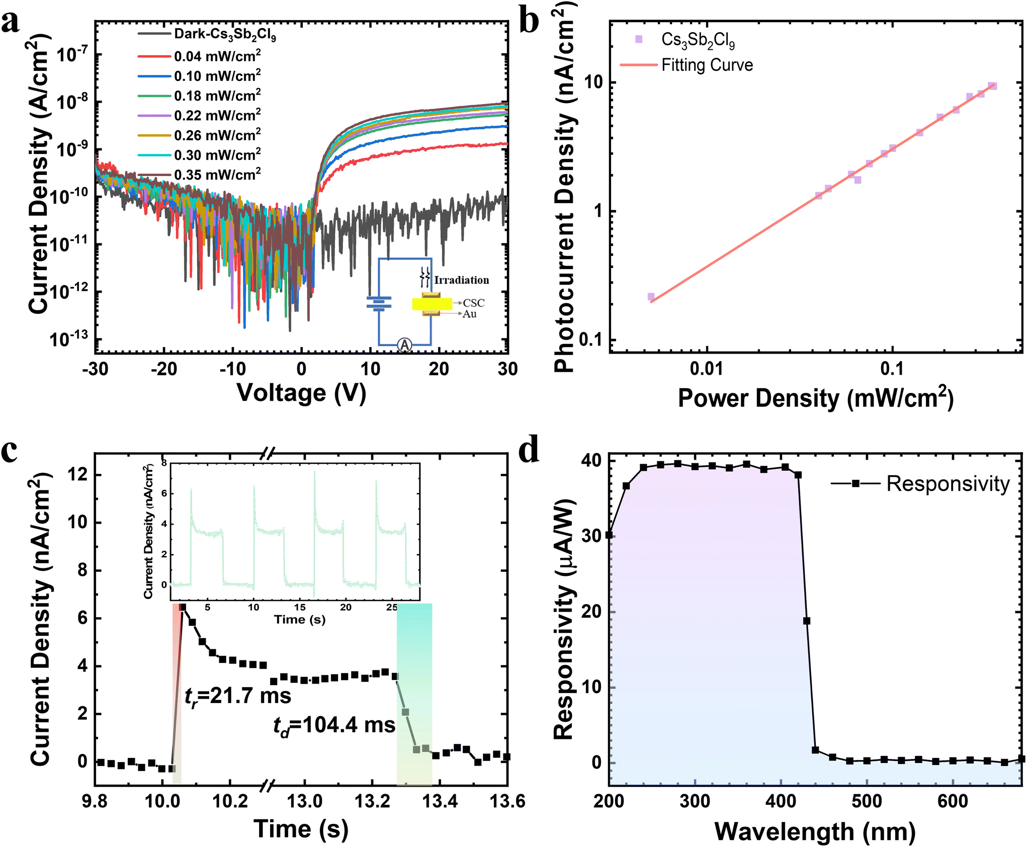 | ||
| Fig. 4 Device performance of Cs3Sb2Cl9 single-crystal photodetectors. (a) I–V curves of the detector in the dark and under different irradiation at 266 nm for bias voltages in the range from −30 V to 30 V. The inset is the device structure. (b) Photocurrent density dependence on the power density of the 266 nm laser. (c) Single photocurrent response cycle with light irradiation ON and OFF, showing rise time (21.7 ms) and decay time (104.4 ms) of the photodetector measured at a bias of 30 V and a light intensity of 0.30 mW cm−2. The inset is the time response of the photodetector with a light irradiance of 0.30 mW cm−2. (d) Responsivity of a Cs3Sb2Cl9 single-crystal photodetector as a function of wavelength. | ||
The relationship between the photocurrent density (Jph) and the irradiance power density (P) can be well fitted by the power law, i.e., Jph ∝ Pα, with an ideal index α of 0.96, as depicted in Fig. 4b. The fitting factor is very close to the ideal value of 1, implying that there is no space-charge limit effect or defect induced recombination.53,54 The time response behaviors of the as-prepared photodetectors were determined by periodically turning on and off the 266 nm laser beam under ambient conditions at a drain voltage of 30 V, as shown in the inset of Fig. 4c. When the pulsed laser is on, the current curve rises very sharply and rapidly, and when it is off, the current intensity quickly returns to the normal dark current value. The photodetector shows a good cycling response and repeatability upon multiple switching cycles. Herein, the rise time and decay time of the photodetector are defined as the time taken for the initial current to increase or decrease to 90% of the peak value, respectively. As shown in Fig. 4c, the rise time is 21.7 ms after triggering and the decay time is 104.4 ms after termination of irradiation. The response speed is consistent with the reported lead-free PVK PDs.11,55,56 Key performance parameters of the typical lead-free PVK PDs reported previously,11,42,53–60 as well as our Cs3Sb2Cl9 single crystal devices are listed in Table 1. As shown in Table 1, Bi-based single-crystal PDs are more common, while Sb-based PDs are mainly prepared using nanocrystals, nanoplates, nanowires, and thin films, and Sb-based single-crystal PD is less reported. Compared with thin films and nanowires, charge carrier lifetimes in single crystals are longer due to less defects and hence a lower trap-induced recombination rate, while the carriers in single crystals can be smoothly transported through shorter paths, which shortens the transport time and improves the response speed, making single crystals more favorable for preparing PDs.1 Compared to the Cs3Sb2Cl9 nanowires-based PDs11 with a rise time of 130 ms and a decay time of 230 ms, the Cs3Sb2Cl9 single-crystal PD exhibits a shorter response time, which is a good demonstration that high-quality single crystals can improve the response speed.
 | (3) |
| Photodetector | Bandgap (eV) | Voltage (V) | Wavelength of light source (nm) | On–off ratio | Rise time (ms) | Decay time (ms) | Responsivity (A W−1) | Ref. |
|---|---|---|---|---|---|---|---|---|
| Notes: single crystals (SC), thin films (TF), microcrystals (MC), microplates (MP), nanowires (NW), nanoplates (NP). | ||||||||
| Cs3BiBr6 SC | 2.55 | 6 | 400 | 3 | 50 | 60 | 2.5 × 10⁻⁵ | 55 |
| Cs3Bi2I9 SCTF | 2.13 | −2 | White light | 11000 |
0.247 | 0.230 | 7.2 × 10⁻³ | 57 |
| Cs3Bi2I9 SC | 1.96 | 10 | 462 | 1000 | — | — | 1.1 | 58 |
| Cs3Bi2I9 SC | 1.94 | 10 | 420 | 24 | — | — | 1.2 × 10⁻³ | 42 |
| Cs3Sb2I9 MP | 2.10 | 1.5 | 450 | 105 | 0.149 | 0.158 | 0.446 | 59 |
| Cs3Sb2I9−xClx TF | 1.99 | 0 | 505 | 106 | — | — | 0.205 | 54 |
| Cs3Sb2I9 MP | 2.24 | 1 | 532 | 104 | 0.096 | 0.058 | 0.01 | 60 |
| Cs3Sb2Br9 NP | 2.65 | 10 | 450 | — | 48 | 24 | 3.8 | 56 |
| Cs3Sb2Br9 SC | 2.26 | 6 | 480 | 104 | 0.2 | 3.0 | 2.29 | 53 |
| Cs3Sb2Cl9 NW | 3.40 | 0.9 | 410 | — | 130 | 230 | 3616 | 11 |
| Cs3Sb2Cl9 SC | 2.86 | 30 | 266 | 103 | 21.7 | 104.4 | 3.95 × 10⁻⁵ | This Work |
The responsivity is expressed as eqn (3), where R is the responsivity, Ilight and Idark are the photocurrent (A) and the dark current (A), respectively, P is the incident light intensity (W cm−2), and S is the effective illuminated area (cm2). The responsivity of Cs3Sb2Cl9 single crystal PD reaches 3.95 × 10⁻⁵ A W−1 under 266 nm laser irradiation at 30 V with a low irradiance of 0.005 mW cm−2. The value of responsivity is of the same order of magnitude as the value of 2.5 × 10⁻⁵ A W−1 for the Cs3BiCl6 single crystal PD at 6 V.55 Compared to iodine- and bromine-based halide perovskites, the surface states of chlorine-based perovskites are often not so stable and are more susceptible to deterioration under an air atmosphere. This relatively low responsivity may result from severe surface recombination at the interface of the Cs3Sb2Cl9 single crystal and the Au electrode. The spectral responsivity of the photodetector under the ambient environment is shown in Fig. 4d. A very sharp cutoff in the spectral responsivity wavelength can be observed at around 430 nm, corresponding to a photon energy of 2.88 eV. This result agrees well with the absorbance and transmittance spectra of Cs3Sb2Cl9 single crystal shown in Fig. 3a, indicating that the detector has obvious wavelength selectivity and shows good sensitivity to UV light. The UV (360 nm) to visible (480 nm) rejection ratio (R360/R480) is about 150, indicating an intrinsic visible-blind characteristic of the Cs3Sb2Cl9 single crystal UV detector.
Conclusions
In summary, the issue of low solubility of CSC materials has been overcome by using a hybrid solvent consisting of DMSO and hydrochloric acid, and limpid perovskite precursor solutions with high solubility have been successfully prepared. Centimeter-sized high-quality α-Cs3Sb2Cl9 and Cs5Sb2Cl11 single crystals have been prepared via the controlled gradient cooling temperature crystallization method using the prepared hybrid solvent. These as-grown single crystals exhibited superior optical and electrical characteristics, and are ideal materials for detecting UV light. The α-Cs3Sb2Cl9 single-crystal photodetector shows a low dark current density of 91 pA cm−2 at a bias of 30 V, a high UV/visible rejection ratio of 150, a high photo-to-dark current ratio of two orders of magnitude and a fast response speed with a rise time of 21.7 ms and a decay time of 104.4 ms. All results demonstrate that the α-Cs3Sb2Cl9 single crystal photodetector is a competitive candidate for the application of visible-blind UV detectors. In addition, the successful use of hybrid solvents to enhance solubility suggests the potential for their application to the growth of all chlorine-based perovskite single crystals, thereby facilitating future exploration of these materials in optoelectronic devices.Author contributions
Conceptualization: W. Wang, S. Xu, and R. Xu; data curation and methodology: W. Wang, S. Xu, Z. Lai, X. Feng, H. Qi, Q. Pan, Z. Yang, J. Kang, Y. Li, X. Shu, and J. Bai; formal analysis, investigation and funding acquisition: W. Wang and R. Xu; visualization: W. Wang, H. Qi, Z. Zhang, and F. Hong; supervision and validation: R. Xu and L. Wang; writing—original draft: W. Wang; writing—review & editing: W. Wang, F. Hong, R. Xu, J. Qin, Y. Zhu, F. Xu, and Y. He.Conflicts of interest
There are no conflicts to declare.Acknowledgements
This work was supported by the National Natural Science Foundation of China (Grant No. 12175131), the Postdoctoral Research Foundation of China (Grant No. 2021M692021), and the Hebei Provincial Key Research Project (Grant No. 20311009D).References
- G. Maculan, A. D. Sheikh, A. L. Abdelhady, M. I. Saidaminov, M. A. Haque, B. Murali, E. Alarousu, O. F. Mohammed, T. Wu and O. M. Bakr, CH3NH3PbCl3 Single Crystals: Inverse Temperature Crystallization and Visible-Blind UV-Photodetector, J. Phys. Chem. Lett., 2015, 6, 3781–3786 CrossRef CAS PubMed.
- H. Wei, Y. Fang, P. Mulligan, W. Chuirazzi, H.-H. Fang, C. Wang, B. R. Ecker, Y. Gao, M. A. Loi, L. Cao and J. Huang, Sensitive X-ray detectors made of methylammonium lead tribromide perovskite single crystals, Nat. Photonics, 2016, 10, 333–339 CrossRef CAS.
- M. I. Saidaminov, M. A. Haque, J. Almutlaq, S. Sarmah, X.-H. Miao, R. Begum, A. A. Zhumekenov, I. Dursun, N. Cho, B. Murali, O. F. Mohammed, T. Wu and O. M. Bakr, Inorganic Lead Halide Perovskite Single Crystals: Phase-Selective Low-Temperature Growth, Carrier Transport Properties, and Self-Powered Photodetection, Adv. Opt. Mater., 2017, 5, 1600704 CrossRef.
- B. Zhou, D. Ding, Y. Wang, S. Fang, Z. Liu, J. Tang, H. Li, H. Zhong, B. Tian and Y. Shi, A Scalable H2O–DMF–DMSO Solvent Synthesis of Highly Luminescent Inorganic Perovskite–Related Cesium Lead Bromides, Adv. Opt. Mater., 2021, 9, 2001435 CrossRef CAS.
- M. Deng, Z. Li, X. Deng, Y. Hu and X. Fang, Wafer-scale heterogeneous integration of self-powered lead-free metal halide UV photodetectors with ultrahigh stability and homogeneity, J. Mater. Sci. Technol., 2023, 164, 150–159 CrossRef.
- Z. Li, T. Yan and X. Fang, Low-dimensional wide-bandgap semiconductors for UV photodetectors, Nat. Rev. Mater., 2023, 8, 587–603 CrossRef.
- P. Gui, H. Zhou, F. Yao, Z. Song, B. Li and G. Fang, Space–Confined Growth of Individual Wide Bandgap Single Crystal CsPbCl3 Microplatelet for Near–Ultraviolet Photodetection, Small, 2019, 15, 1902618 CrossRef PubMed.
- J. Dziedzic, J. Mróz and R. Jakubas, Pyroelectric and dilatometric studies on the low temperature ferroelectric phase transition of (CH3NH3)5Bi2Br11, Acta Phys. Pol., A, 2005, 108, 505–511 CrossRef CAS.
- C. Wu, Q. Zhang, G. Liu, Z. Zhang, D. Wang, B. Qu, Z. Chen and L. Xiao, From Pb to Bi: A Promising Family of Pb–Free Optoelectronic Materials and Devices, Adv. Energy Mater., 2019, 10, 1902496 CrossRef.
- K. Kihara and T. Sudo, Two structure types of cesium antimony nonachloride, Cs3Sb2Cl9, Z. Kristallogr., 1971, 134, 155–158 CAS.
- B. Pradhan, G. S. Kumar, S. Sain, A. Dalui, U. K. Ghorai, S. K. Pradhan and S. Acharya, Size Tunable Cesium Antimony Chloride Perovskite Nanowires and Nanorods, Chem. Mater., 2018, 30, 2135–2142 CrossRef CAS.
- A. Pradhan, S. C. Sahoo, A. K. Sahu and S. L. Samal, Effect of Bi Substitution on Cs3Sb2Cl9: Structural Phase Transition and Band Gap Engineering, Cryst. Growth Des., 2020, 20, 3386–3395 CrossRef CAS.
- A. Singh, N. C. Chiu, K. M. Boopathi, Y. J. Lu, A. Mohapatra, G. Li, Y. F. Chen, T. F. Guo and C. W. Chu, Lead-Free Antimony-Based Light-Emitting Diodes through the Vapor-Anion-Exchange Method, ACS Appl. Mater. Interfaces, 2019, 11, 35088–35094 CrossRef CAS PubMed.
- X. Wang, N. Ali, G. Bi, Y. Wang, Q. Shen, A. Rahimi-Iman and H. Wu, Lead-Free Antimony Halide Perovskite with Heterovalent Mn2+ Doping, Inorg. Chem., 2020, 59, 15289–15294 CrossRef CAS PubMed.
- B. Ptaszyński, Thermoanalytical studies of compounds of general formula Cs3[SbxBi2−xCl9], Thermochim. Acta, 1987, 116, 225–233 CrossRef.
- B. Ptaszyński, A study of thermal decomposition of complex compounds of Cs3[Sb2−xPbxCl9−x] type, Thermochim. Acta, 1988, 130, 299–307 CrossRef.
- G. Kresse and J. Furthmüller, Efficient iterative schemes for ab initio total-energy calculations using a plane-wave basis set, Phys. Rev. B: Condens. Matter Mater. Phys., 1996, 54, 11169–11186 CrossRef CAS PubMed.
- C. Freysoldt, B. Grabowski, T. Hickel, J. Neugebauer, G. Kresse, A. Janotti and C. G. Van de Walle, First-principles calculations for point defects in solids, Rev. Mod. Phys., 2014, 86, 253–305 CrossRef.
- R. P. Oertel, Vibrational spectra of dimethyl sulfoxide complexes of antimony(III) and bismuth(III) halides, Spectrochim. Acta, Part A, 1970, 26, 659–669 CrossRef CAS.
- J. C. Hamill, J. Schwartz and Y.-L. Loo, Influence of Solvent Coordination on Hybrid Organic–Inorganic Perovskite Formation, ACS Energy Lett., 2017, 3, 92–97 CrossRef.
- P. K. Nayak, D. T. Moore, B. Wenger, S. Nayak, A. A. Haghighirad, A. Fineberg, N. K. Noel, O. G. Reid, G. Rumbles, P. Kukura, K. A. Vincent and H. J. Snaith, Mechanism for rapid growth of organic-inorganic halide perovskite crystals, Nat. Commun., 2016, 7, 13303 CrossRef CAS PubMed.
- M. A. Flatken, E. Radicchi, R. Wendt, A. G. Buzanich, E. Härk, J. Pascual, F. Mathies, O. Shargaieva, A. Prause, A. Dallmann, F. De Angelis, A. Hoell and A. Abate, Role of the Alkali Metal Cation in the Early Stages of Crystallization of Halide Perovskites, Chem. Mater., 2022, 34, 1121–1131 CrossRef CAS.
- M. Fontana, G. Maisano, P. Migliardo, C. Vasi and F. Wanderlingh, Raman Scattering and Melting Point in SbCl3, Optica Acta: Int J Opt, 1980, 27, 1087–1093 CrossRef CAS.
- J. Milne, Spectrophotometric Studies on Sb(III) in Hydrochloric Acid Solutions, Can. J. Chem., 1975, 53, 888–893 CrossRef CAS.
- W. Wang, H. Meng, H. Qi, H. Xu, W. Du, Y. Yang, Y. Yi, S. Jing, S. Xu, F. Hong, J. Qin, J. Huang, Z. Xu, Y. Zhu, R. Xu, J. Lai, F. Xu, L. Wang and J. Zhu, Electronic-Grade High-Quality Perovskite Single Crystals by a Steady Self-Supply Solution Growth for High-Performance X-ray Detectors, Adv. Mater., 2020, 32, 2001540 CrossRef CAS PubMed.
- B. Vargas, E. Ramos, E. Pérez-Gutiérrez, J. C. Alonso and D. Solis-Ibarra, A Direct Bandgap Copper−Antimony Halide Perovskite, J. Am. Chem. Soc., 2017, 139, 9116–9119 CrossRef CAS PubMed.
- B. Saparov, F. Hong, J.-P. Sun, H.-S. Duan, W. Meng, S. Cameron, I. G. Hill, Y. Yan and D. B. Mitzi, Thin-Film Preparation and Characterization of Cs3Sb2I9: A Lead-Free Layered Perovskite Semiconductor, Chem. Mater., 2015, 27, 5622–5632 CrossRef CAS.
- P. E. Tomaszewski, Crystal Structure and Phase Transitions in the A3B2X9 Family of Crystals, Phys. Status Solidi B, 1994, 181, 15–21 CrossRef CAS.
- R. Jakubas, A new ferroelectric compound (CH3NH3)5Bi2Br11, Solid State Commun., 1989, 69, 267–269 CrossRef CAS.
- R. Jakubas, L. Sobczyk and J. Lefebvre, A new ferroelectric crystal (CH3NH3)5Bi2Cl11, Ferroelectrics, 1989, 100, 143–149 CrossRef CAS.
- J. Mróz and R. Jakubas, Ferroelectricity in (CH3NH3)5Bi2Br11 crystals, Solid State Commun., 1989, 72, 813–816 CrossRef.
- J. Lefebvre, P. Carpentier and R. Jakubas, Structures and phase transition in the ferroelectric crystal of pentakis(methylammonium) undecachlorodibismuthate(III) [NH3(CH3)]5Bi2Cl11, Acta Crystallogr., Sect. B: Struct. Sci., 1991, 47, 228–234 CrossRef.
- Y. Liu, Y. Zhang, Z. Yang, J. Feng, Z. Xu, Q. Li, M. Hu, H. Ye, X. Zhang, M. Liu, K. Zhao and S. Liu, Low-temperature-gradient crystallization for multi-inch high-quality perovskite single crystals for record performance photodetectors, Mater. Today, 2019, 22, 67–75 CrossRef CAS.
- B. Su, M. Li, E. Song and Z. Xia, Sb3+ Doping in Cesium Zinc Halides Single Crystals Enabling High–Efficiency Near–Infrared Emission, Adv. Funct. Mater., 2021, 31, 2105316 CrossRef CAS.
- R. Xu, Z. Hong, X. Tong, W. Wang, H. Meng, J. Qin, X. Wang, X. Shu, J. Cai, Z. Zhang, F. Xu, H. Xu, F. Hong, H. Qi, J. Lai and D. Li, Uncovering the Formation Mechanism of Striations and Pyramidal Pits on a Native MAPbI3 Single-Crystal Surface, J. Phys. Chem. C, 2022, 126, 7319–7325 CrossRef CAS.
- Y. Yuan, R. Xu, H. Xu, F. Hong, F. Xu and L. Wang, Nature of the band gap of halide perovskites ABX3 (A = CH3NH3,Cs; B = Sn, Pb; X = Cl, Br, I): First-principles calculations, Chin. Phys. B, 2015, 24, 116302 CrossRef.
- D. O. Scanlon, C. W. Dunnill, J. Buckeridge, S. A. Shevlin, A. J. Logsdail, S. M. Woodley, C. R. Catlow, M. J. Powell, R. G. Palgrave, I. P. Parkin, G. W. Watson, T. W. Keal, P. Sherwood, A. Walsh and A. A. Sokol, Band alignment of rutile and anatase TiO2, Nat. Mater., 2013, 12, 798–801 CrossRef CAS PubMed.
- Z. Yang, W. Meng, J. Kang, X. Wang, X. Shu, T. Chen, R. Xu, F. Xu and F. Hong, Unraveling the Defect-Dominated Broadband Emission Mechanisms in (001)-Preferred Two-Dimensional Layered Antimony-Halide Perovskite Film, J. Phys. Chem. Lett., 2022, 13, 11736–11744 CrossRef CAS PubMed.
- K. M. McCall, Z. Liu, G. Trimarchi, C. C. Stoumpos, W. Lin, Y. He, I. Hadar, M. G. Kanatzidis and B. W. Wessels, α-Particle Detection and Charge Transport Characteristics in the A3M2I9 Defect Perovskites (A = Cs, Rb; M = Bi, Sb), ACS Photonics, 2018, 5, 3748–3762 CrossRef CAS.
- L. Zhou, J. Liao, Z. Huang, J. Wei, X. Wang, H. Chen and D. Kuang, Intrinsic Self-Trapped Emission in 0D Lead-Free (C4H14N2)2In2Br10 Single Crystal, Angew. Chem., Int. Ed., 2019, 58, 15435–15440 CrossRef CAS PubMed.
- X. Li, X. Du, P. Zhang, Y. Hua, L. Liu, G. Niu, G. Zhang, J. Tang and X. Tao, Lead-free halide perovskite Cs3Bi2Br9 single crystals for high-performance X-ray detection, Sci. China Mater., 2021, 64, 1427–1436 CrossRef CAS.
- H. Zhang, Y. Xu, Q. Sun, J. Dong, Y. Lu, B. Zhang and W. Jie, Lead free halide perovskite Cs3Bi2I9 bulk crystals grown by a low temperature solution method, CrystEngComm, 2018, 20, 4935–4941 RSC.
- H. Li, J. Song, W. Pan, D. Xu, W. Zhu, H. Wei and B. Yang, Sensitive and Stable 2D Perovskite Single-Crystal X-ray Detectors Enabled by a Supramolecular Anchor, Adv. Mater., 2020, 32, 2003790 CrossRef CAS PubMed.
- A. CiŻman, R. Poprawski and A. Sieradzki, Ferroelectric phase transition in (CH3NH3)5Bi2Cl11 and (CH3NH3)5Bi2Br11 crystals, Phase Transitions, 2007, 80, 171–176 CrossRef.
- J. Tauc, R. Grigorovici and A. Vancu, Optical Properties and Electronic Structure of Amorphous Germanium, Phys. Status Solidi B, 1966, 15, 627–637 CrossRef CAS.
- J. Luo, X. Wang, S. Li, J. Liu, Y. Guo, G. Niu, L. Yao, Y. Fu, L. Gao, Q. Dong, C. Zhao, M. Leng, F. Ma, W. Liang, L. Wang, S. Jin, J. Han, L. Zhang, J. Etheridge, J. Wang, Y. Yan, E. H. Sargent and J. Tang, Efficient and stable emission of warm-white light from lead-free halide double perovskites, Nature, 2018, 563, 541–545 CrossRef CAS PubMed.
- S. Li, J. Luo, J. Liu and J. Tang, Self-Trapped Excitons in All-Inorganic Halide Perovskites: Fundamentals, Status, and Potential Applications, J. Phys. Chem. Lett., 2019, 10, 1999–2007 CrossRef CAS PubMed.
- H.-H. Fang, S. Adjokatse, H. Wei, J. Yang, G. R. Blake, J. Huang, J. Even and M. A. Loi, Ultrahigh sensitivity of methylammonium lead tribromide perovskite single crystals to environmental gases, Mat. Sci., 2016, 2, 1–9 Search PubMed.
- D. Shi, V. Adinolfi, R. Comin, M. Yuan, E. Alarousu, A. Buin, Y. Chen, S. Hoogland, A. Rothenberger, K. Katsiev, Y. Losovyj, X. Zhang, P. A. Dowben, O. F. Mohammed, E. H. Sargent and O. M. Bakr, Low trap-state density and long carrier diffusion in organolead trihalide perovskite single crystals, Science, 2015, 347, 519–522 CrossRef CAS PubMed.
- Y. Jiang, M. Cui, S. Li, C. Qin, Y. Liu and M. Yuan, Reducing the impact of Auger recombination in quasi-2D perovskite light-emitting diodes, Nat. Commun., 2021, 12, 1–10 CrossRef PubMed.
- M. Keshavarz, E. Debroye, M. Ottesen, C. Martin, H. Zhang, E. Fron, R. Kuchler, J. A. Steele, M. Bremholm, J. Van de Vondel, H. I. Wang, M. Bonn, M. B. J. Roeffaers, S. Wiedmann and J. Hofkens, Tuning the Structural and Optoelectronic Properties of Cs2 AgBiBr6 Double-Perovskite Single Crystals through Alkali-Metal Substitution, Adv. Mater., 2020, 32, 2001878 CrossRef CAS PubMed.
- Y. Feng, L. Pan, H. Wei, Y. Liu, Z. Ni, J. Zhao, P. N. Rudd, L. R. Cao and J. Huang, Low defects density CsPbBr3 single crystals grown by an additive assisted method for gamma-ray detection, J. Mater. Chem. C, 2020, 8, 11360–11368 RSC.
- P. Liu, Y. Liu, S. Zhang, J. Li, C. Wang, C. Zhao, P. Nie, Y. Dong, X. Zhang, S. Zhao and G. Wei, Lead–Free Cs3Sb2Br9 Single Crystals for High Performance Narrowband Photodetector, Adv. Opt. Mater., 2020, 8, 2001072 CrossRef CAS.
- J. Mei, M. Liu, P. Vivo and V. Pecunia, Two–Dimensional Antimony–Based Perovskite–Inspired Materials for High–Performance Self–Powered Photodetectors, Adv. Funct. Mater., 2021, 31, 2106295 CrossRef CAS.
- Y. Tang, M. Liang, B. Chang, H. Sun, K. Zheng, T. Pullerits and Q. Chi, Lead-free double halide perovskite Cs3BiBr6 with well-defined crystal structure and high thermal stability for optoelectronics, J. Mater. Chem. C, 2019, 7, 3369–3374 RSC.
- Z. Zheng, Q. Hu, H. Zhou, P. Luo, A. Nie, H. Zhu, L. Gan, F. Zhuge, Y. Ma, H. Song and T. Zhai, Submillimeter and lead-free Cs3Sb2Br9 perovskite nanoflakes: inverse temperature crystallization growth and application for ultrasensitive photodetectors, Nanoscale Horiz., 2019, 4, 1372–1379 RSC.
- W. G. Li, X. D. Wang, J. F. Liao, Y. Jiang and D. B. Kuang, Enhanced On–Off Ratio Photodetectors Based on Lead–Free Cs3Bi2I9 Single Crystal Thin Films, Adv. Funct. Mater., 2020, 30, 1909701 CrossRef CAS.
- Y. Zhang, Y. Liu, Z. Xu, H. Ye, Z. Yang, J. You, M. Liu, Y. He, M. G. Kanatzidis and S. F. Liu, Nucleation-controlled growth of superior lead-free perovskite Cs3Bi2I9 single-crystals for high-performance X-ray detection, Nat. Commun., 2020, 11, 2304 CrossRef CAS PubMed.
- Z. Lai, Y. Meng, F. Wang, X. Bu, W. Wang, P. Xie, W. Wang, C. Liu, S. Yip and J. C. Ho, Direct drop-casting synthesis of all-inorganic lead and lead-free halide perovskite microcrystals for high-performance photodetectors, Nano Res., 2021, 15, 3621–3627 CrossRef.
- S. K. Shil, F. Wang, Z. Lai, Y. Meng, Y. Wang, D. Zhao, M. K. Hossain, K. O. Egbo, Y. Wang, K. M. Yu and J. C. Ho, Crystalline all-inorganic lead-free Cs3Sb2I9 perovskite microplates with ultra-fast photoconductive response and robust thermal stability, Nano Res., 2021, 14, 4116–4124 CrossRef CAS.
Footnote |
| † Electronic supplementary information (ESI) available: Solubilities in different solvents, Tyndall effect, crystal structure, XRF, XPS, PL intensity and FWHM, and electronic performance. See DOI: https://doi.org/10.1039/d3qi02153j |
| This journal is © the Partner Organisations 2024 |