
 Open Access Article
 This Open Access Article is licensed under a
 Creative Commons Attribution 3.0 Unported Licence
Sb 5s2 lone pairs and band alignment of Sb2Se3: a photoemission and density functional theory study†
Christopher H.
Don‡
a,
Huw
Shiel‡
a,
Theodore D. C.
Hobson
 a,
Christopher N.
Savory
bc,
Jack E. N.
Swallow
a,
Matthew J.
Smiles
a,
Leanne A. H.
Jones
a,
Thomas J.
Featherstone
a,
Pardeep K.
Thakur
d,
Tien-Lin
Lee
d,
Ken
Durose
d,
Jonathan D.
Major
a,
Vinod R.
Dhanak
a,
David O.
Scanlon
bcd and
Tim D.
Veal
*a
a,
Christopher N.
Savory
bc,
Jack E. N.
Swallow
a,
Matthew J.
Smiles
a,
Leanne A. H.
Jones
a,
Thomas J.
Featherstone
a,
Pardeep K.
Thakur
d,
Tien-Lin
Lee
d,
Ken
Durose
d,
Jonathan D.
Major
a,
Vinod R.
Dhanak
a,
David O.
Scanlon
bcd and
Tim D.
Veal
*a
aStephenson Institute for Renewable Energy and Department of Physics, University of Liverpool, Liverpool L69 7ZF, UK. E-mail: T.Veal@liverpool.ac.uk
bDepartment of Chemistry, University College London, 20 Gordon Street, London WC1H 0AJ, UK
cThomas Young Centre, University College London, Gower Street, London WC1E 6BT, UK
dDiamond Light Source Ltd, Diamond House, Harwell Science and Innovation Campus, Didcot, Oxfordshire OX11 0DE, UK
First published on 18th August 2020
Abstract
The presence of a lone pair of 5s electrons at the valence band maximum (VBM) of Sb2Se3 and the resulting band alignments are investigated using soft and hard X-ray photoemission spectroscopy in parallel with density functional theory (DFT) calculations. Vacuum-cleaved and exfoliated bulk crystals of Sb2Se3 are analysed using laboratory and synchrotron X-ray sources to acquire high resolution valence band spectra with both soft and hard X-rays. Utilising the photon-energy dependence of different orbital cross-sections and corresponding DFT calculations, the various orbital contributions to the valence band could be identified, including the 5s orbital's presence at the VBM. The ionization potential is also determined and places the VBM at 5.13 eV below the vacuum level, similar to other materials with 5s2 lone pairs, but far above those of related materials without lone pairs of electrons.
1 Introduction
Antimony selenide (Sb2Se3) is a candidate thin film photovoltaic (PV) material, which has the desirable properties of being Earth abundant, low toxicity and stable.1Beyond that, the material has relatively simple low-cost production methods due to it being a binary V–VI compound and its potential as a thin-film PV absorber is high due to its high absorption coefficient (>105 cm−1 below 2 eV), which is 1000 times greater than that of silicon.3,4 This makes it of great interest to those seeking to diversify the field of photovoltaics and find a scalable thin film technology to aid in achieving the target of terawatt scale-up. It has also attracted attention in the field of photocatalytic hydrogen evolution.5–7 A recent paper reports a direct band gap for Sb2Se3 of 1.180 eV at 320 K, increasing to 1.316 eV at 20 K (ref. 8), nearly ideal for a single-junction device. The maximum recorded solar cell power conversion efficiency (PCE) for this material has already reached 9.2% using core–shell structured nanorod array solar cells,9 and the improvement has been rapid as efficiencies of just 2.1% were reported in 2014 (ref. 10). The number of papers published on Sb2Se3 is now increasing exponentially and several labs have now independently reported planar Sb2Se3 solar cells with PCE in excess of 6% (ref. 11–19).
One of the most intriguing properties of Sb2Se3 is its one-dimensional nanoribbon structure as shown in Fig. 1. Strongly covalently bonded ‘ribbons’ along the c-axis are held together parallel to each other by weaker van der Waals interactions. It has been reported that this ribbon structure causes anisotropic conductivity in the bulk material because of the low carrier mobility across ribbons, resulting in crystal orientation-dependence of the solar cell performance of this material, along with potential benign or self-healing grain boundaries.15,20 The origin of this anisotropic crystal structure is attributed to the presence of a stereochemically active ns2 lone pair orbital at the upper edge of the valence band, a property that has been shown to have a significant influence on the optoelectronic properties of materials possessing it.21–24
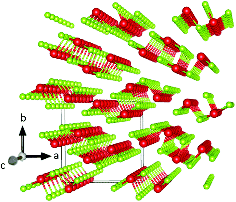 | ||
| Fig. 1 Sb2Se3 crystal structure drawn in VESTA 3 (ref. 2) – antimony atoms are shown in red and selenium atoms in green. The solid line cuboid represents the unit cell. The axes labels correspond to the Pbnm setting of space group 62. | ||
The aim of this study is to show experimentally the presence of a stereochemically active lone pair orbital at the valence band edge of Sb2Se3 and how this influences the ionization potential and natural band alignment of the material. The ionization potential – the separation between valence band maximum and vacuum level – for Sb2Se3 was measured using X-ray photoemission spectroscopy (XPS) (hν = 1.487 keV) of the valence band and secondary electron cutoff. Valence-band and core-level data were obtained from an Sb2Se3 bulk crystal, exposed to surface oxidation effects and cleaved in vacuum, using hard X-ray photoemission spectroscopy (HAXPES) (hν = 5.921 keV). As well as providing slightly better spectral resolution than conventional lab-based XPS, the synchrotron photoemission beamline could be adjusted to deliver soft X-rays (hν = 0.800 keV) to the same position on the crystal, without changing any other experimental conditions. Using multiple energies allows for the exploitation of the photon-energy-dependence of the orbital cross-sections. This can be used to discriminate between different orbitals within the valence band when comparing to density functional theory (DFT) calculations.
The energy dependence of photoionization cross-sections refers to the way in which an orbital's photoionization probability varies with different incident photon energies. The rate of photoemission tends to decrease with increasing incident photon energy (at least sufficiently far from the threshold energy). This decrease is the result of the wavelength of the incident photon becoming more comparable with the radial extension of the valence band orbitals and the resulting cancellation of terms contributing to the transition matrix element. In general, s-orbital photoionization cross-sections decrease more gradually with increasing photon energy relative to other orbitals because of the more contracted nature of the orbitals (see Fig. 2). Therefore, the relative contribution to the valence band photoemission spectrum from s-orbitals is generally expected to be greater in measurements taken with hard X-rays than with soft X-rays. The cross sections for the Sb and Se orbitals are also compared in Table 1 for the two photon energies used in our synchrotron radiation measurements.
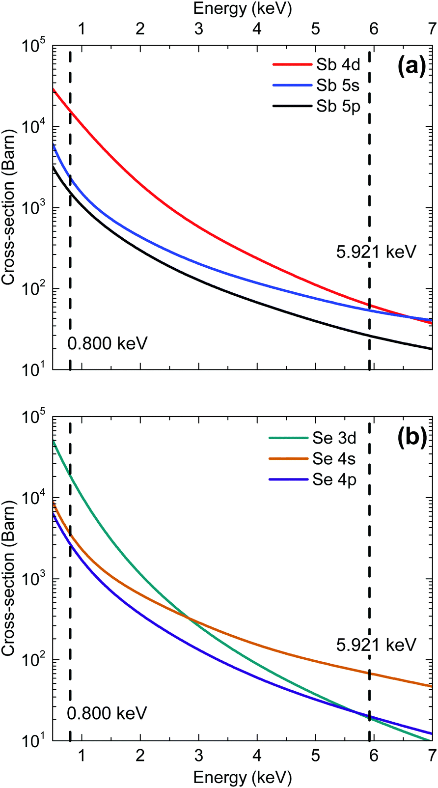 | ||
| Fig. 2 Photoionization cross-section energy dependence for each valence orbital in (a) antimony and (b) selenium.25 | ||
| Orbital | Cross section (barns) | |
|---|---|---|
| 0.800 keV | 5.921 keV | |
| Sb 4d | 15![[thin space (1/6-em)]](https://www.rsc.org/images/entities/char_2009.gif) 466 466 |
63 |
| Sb 5s | 2311 | 54 |
| Sb 5p | 1507 | 26 |
| Se 3d | 18576 |
19 |
| Se 4s | 3600 | 68 |
| Se 4p | 2646 | 20 |
Another area of interest is to what extent surface oxidation of the Sb2Se3 material affects cell performance. Photoemission spectroscopy is a commonly used tool for identifying elemental composition and chemical states present at the surface of a sample. However, the XPS investigations of Sb2Se3 surface oxidation have thus far seen some conflicting results. A 2014 study by Liu et al. stated that the presence of an O 1s peak in their data (532.9 eV) suggests the existence of Sb2O3. However, Sb 3d and Sb 4d states would be expected to exhibit additional chemically shifted components to higher binding energy if this were the case, corresponding to the two different chemical environments present in the sample.10 We therefore argue that the O 1s peak observed is a result of surface physisorbed oxygen that is not interacting chemically with the Sb2Se3 crystal. Further studies carried out in 2017 by Wang et al.26 and Chen et al.27 show conflicting assignments in their reported peak positions of elemental Se, despite both studies coming from the same group, as later highlighted in detail by Shiel et al.13 The XPS interpretation by Shiel et al. is consistent with Wang et al. and others,28,29 though the oxide components only contributed a minor proportion of the measured Sb 3d signals. The results presented here, comparing as-received oxidised crystals with oxygen-free in-vacuum cleaved Sb2Se3 crystals, provide additional information to inform future photoemission analysis of Sb2Se3.
2 Experimental and computational details
The Sb2Se3 single crystals utilised in this work were prepared via the Bridgman melt-growth technique using a single-zone vertical furnace. Granular Sb2Se3 source material (5N purity, Alfa Aesar) was manually ground in a mortar and pestle with the resulting powder placed in a quartz tube with 4 mm internal diameter. The tube was flushed three times with Ar gas then evacuated to ∼10−5 mbar to evaporate residual volatile compounds. The tube was filled with Ar at a pressure of 100 mbar immediately before sealing, intended to suppress the sublimation of Sb2Se3 that occurs at low pressure due to the high vapour pressure of Sb2Se3 (ref. 10). This was necessary to avoid the formation of large gas bubbles in the crystal boules and also to prevent unwanted vapour transport of material away from the melt-grown crystals. The sealed ampoule was placed with the bottom tip in line with the peak of the temperature profile in the furnace and heated to 620 °C (the melting point of Sb2Se3 is 611 °C). It was then held for around 6 hours to allow full melting and homogenisation of the powder. The ampoule was then lowered through the natural temperature gradient of the furnace, at 0.6 °C mm−1 in the working range, towards the lower, open end of the furnace (at room temperature), at a rate of 1.15 mm h−1 for 7 days. The ampoule was rotated at a low speed throughout to ensure homogeneous heating. The identity and crystallographic orientation of Sb2Se3 was confirmed by X-ray diffraction and Raman spectroscopy as described in detail for these crystals by Fleck et al. in ref. 30. Its chemical composition was further confirmed as 40% Sb and 60% Se by energy dispersive X-ray (EDX) analysis in a scanning electron microscope (SEM), this being consistent with the expected 2:3 stoichiometry. An SEM image and some EDX data are shown in Fig. S1 (ESI†). This used an Oxford INCA X-act EDX detector in a JEOL JSM 6610 SEM. The Sb2Se3 manufacturers’ purity was 99.999% by metals basis analysis. We identified chlorine as being the most important non-metallic impurity using secondary ion mass spectroscopy, making the crystals n-type with n = 1017 cm−3 (ref. 31). Extracted crystals were found to cleave easily in one plane to reveal parallel reflective facets, demonstrated to be the (010) crystal plane (using the Pbnm space group setting).32 Given that the weakest van der Waals interactions lie along the b axis, this behaviour is expected.33 This (010) crystal surface was exposed to air and is the “as-received” crystal referred to below as opposed to the “in situ cleaved” crystal which refers to the crystal cleaved in ultrahigh vacuum. For the synchrotron photoemission measurements, this was done by gluing a post to the crystal surface, and cleaving by hitting the post with a wobble stick. For the laboratory XPS measurements, this was done by exfoliating surface layers of the crystal using carbon tape attached to a sample-transfer arm.
Hard X-ray photoemission spectroscopy was carried out at the I09 beamline at the Diamond Light Source facility. X-ray energies of 5.921 keV and 0.800 keV were selected using double-crystal Si(111) monochromator followed by a Si(004) channel-cut crystal. The energy resolution was 250 meV, determined by fitting a Gaussian-broadened Fermi–Dirac distribution to the Fermi edge of a gold reference sample. The spectra were acquired using a Scienta Omicron EW4000 high-energy analyser with an acceptance angle of ±28°. The crystals were first measured as-received and then were cleaved in situ to expose a pristine (010) surface and to prevent any re-oxidation of the surface. All peak positions from curve fitting are reported with an error of ±0.05 eV. XPS was performed using a SPECS monochromatic Al Kα source (hν = 1486.6 eV) and data was collected with a PSP Vacuum Technologies hemispherical electron-energy analyser with an acceptance angle of ±3°. The energy resolution was 400 meV, determined by fitting a Gaussian-broadened Fermi–Dirac distribution to the Fermi edge of a silver reference sample. Photoemission spectra were curve fitted using CASAXPS software with Voigt lineshapes after subtracting a Shirley background.34
DFT calculations were performed within periodic boundary conditions using the Vienna Ab initio Simulation Package (VASP).35–38 The screened hybrid exchange correlation functional HSE06 was used,39 for geometry optimization and electronic structure calculations of Sb2Se3. To account for the ribbon nature of the Sb2Se3 structure, the D3 dispersion correction from Grimme et al. was also included in density of states (DoS) calculations,40 while spin–orbit coupling (SOC) was included for all calculations. A plane wave energy cutoff of 350 eV was used for all calculations, with a Γ-centered k-point mesh with spacing between k-points of 0.27 Å−1 used for bulk calculations of Sb2Se3. These values were obtained through convergence testing on the total energy, using criteria of 1 meV per atom and 10 meV per atom for k-mesh and energy cutoff, respectively. Prior to the calculation of the electronic density of states, the structure was relaxed (during which the plane-wave energy cutoff was increased to 455 eV to avoid errors arising from Pulay stress) with HSE06+D3 until the forces per atom were below 0.01 eV Å−1, which results in lattice parameters in agreement with experiment.41
3 Results
3.1 Core-level HAXPES
Core-level analysis of photoemission measurements allows for the identification of surface chemical composition and the extent to which surface contamination has chemically altered the surface through examination of the chemical shift in characteristic elemental lines. Materials largely unaffected by a moderate level of contamination are favoured since they may not necessarily need manufacturing in ultra clean environments – thus minimising production costs and increasing viability of widespread adoption. Surface contamination can also have an effect on the formation of favourable interfaces in photovoltaic devices.13 Therefore, a good understanding of how to identify these contaminants is essential. A list of core level peak positions and full widths at half maximum (FWHM) values for an as-received and in situ cleaved Sb2Se3 bulk crystal can be found in Table 2.| Peak | As-received | In situ cleaved | ||
|---|---|---|---|---|
| BE (eV) | Width (eV) | BE (eV) | Width (eV) | |
| Sb(Se) 3d5/2 | 529.53 | 0.71 | 529.71 | 0.62 |
| Sb(O) 3d5/2 | 530.72 | 0.90 | — | — |
| Sb(Se) 4d5/2 | 33.41 | 0.56 | 33.47 | 0.46 |
| Sb(O) 4d5/2 | 34.62 | 0.83 | — | — |
| Se(Sb) 3d5/2 | 54.11 | 0.68 | 54.16 | 0.58 |
| Se(Elem.) 3d5/2 | 55.78 | 1.13 | — | — |
| O(Sb) 1s | 530.66 | 0.60 | — | — |
| O(Adv.) 1s | 531.17 | 0.60 | — | — |
Fig. 3 shows Sb 3d3/2 and 3d5/2 peaks before and after in situ cleaving to expose a pristine surface. In both Fig. 3(a) and (b), the agreement between data and the fitted envelope is good. The highest intensity peaks seen in both Fig. 3(a) and (b) are from antimony bonded to selenium (red line). The spectrum recorded from the contaminated sample in Fig. 3(a) is complicated by the overlap of peaks due to the O 1s state (magenta and cyan), as well as chemically shifted Sb 3d states bonded to oxygen (blue lines). This feature is attributed to Sb2O3 due to the 3d5/2 peak position of 530.7 eV coinciding with literature values for Sb2O3.42 Despite this agreement, the evidence is not enough to be conclusive – a previous paper reported Sb 3d3/2 positions of Sb2O3 and Sb2O5 as 539.8 eV and 540.4 eV respectively,43 compared to a position measured here of 540.1 eV. The smallest of the fitted peaks in Fig. 3(a) (cyan) has a measured peak position also of 530.7 eV which broadly agrees with current literature for the O 1s state in an Sb2O3 environment (529.8 eV)44 and this same conclusion has been reached in related work.24 The remaining O 1s peak (magenta) has been labelled as adventitious oxygen weakly adsorbed on the surface, but could also be a result of atmospheric CO2 surface physisorption. However, the position of the carbon 1s peak at 285.4 eV, indicates this is unlikely. The assignment of all these extra peaks in Fig. 3(a) to oxygen-related species caused by atmospheric exposure is further supported by the data from the in situ cleaved crystal in Fig. 3(b) which shows only clean, sharply defined selenium bound antimony 3d peaks in this binding energy region.
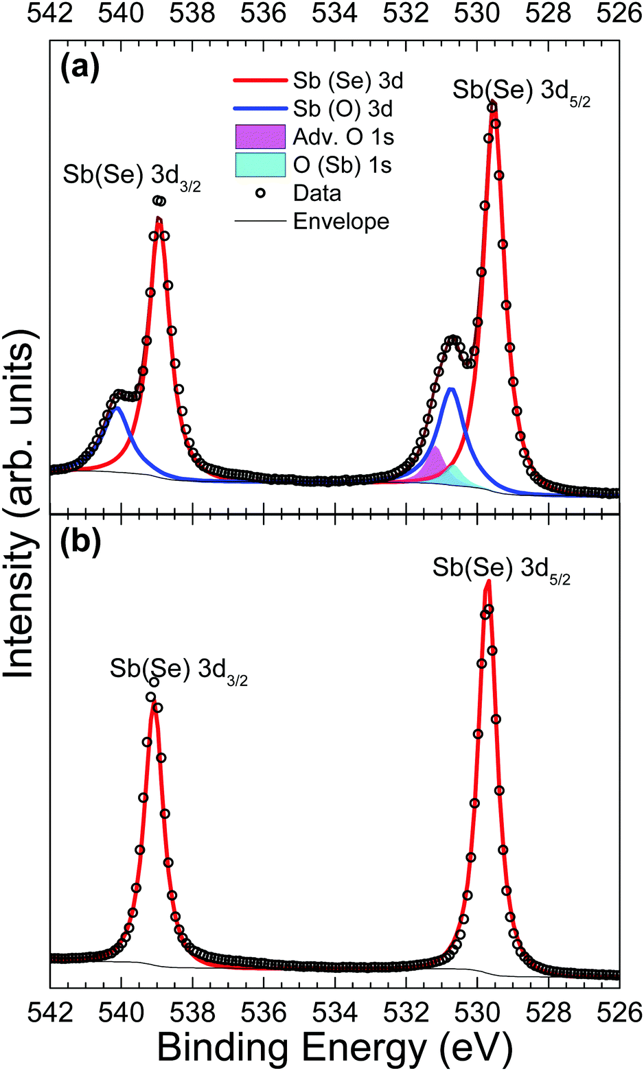 | ||
| Fig. 3 Sb 3d HAXPES data from an Sb2Se3 crystal (a) before and (b) after in situ cleaving. | ||
A comparison of Se 3d data from a contaminated as-received and an in situ cleaved crystal is presented in Fig. 4. Unfortunately, the spectra are complicated by the presence of plasmon loss features from the Sb 4d states. The valence band plasmon energy is found to be 17.9 eV. This is confirmed by the observation of loss features at a binding energy 17.9 eV higher than each core level peak, as shown in the survey scan in Fig. S2 of the ESI.† However, these have been accounted for by fitting them according to the same doublet separation and FWHM of the Sb 4d core levels. It was initially thought that the chemically shifted peaks in Fig. 4a (blue line) were caused by SeO2 states, similar to those seen in the Sb 3d data, however related literature suggests that a SeO2 chemically shifted Se 3d5/2 peak should appear at higher binding energy (∼59 eV29,45,46) than that observed. Shiel et al. identified these peaks as free elemental selenium13 which corresponds well with the presence of Sb2O3 seen in the Sb 3d state; since the selenium from the pure Sb2Se3 crystal must become unbound when it is replaced by oxygen to form the Sb2O3 on the surface. As expected, the peaks associated with elemental Se are also absent after in situ cleaving, further confirming that exposure to standard atmospheric conditions does not impact the bulk chemistry of the material, only the surface.
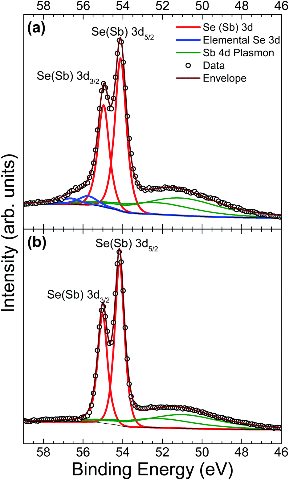 | ||
| Fig. 4 Se 3d HAXPES data from an Sb2Se3 crystal (a) before and (b) after in situ cleaving. | ||
3.2 Valence band photoemission
Valence band (VB) spectra were obtained by collecting photoelectrons excited by monochromatic X-rays of 5.921 keV both before and after in situ cleaving of the crystal, to look at the effects of surface contamination on VB states. An additional data set was taken from the in situ cleaved crystal at a softer X-ray energy of 0.800 keV to utilise the energy dependence of photoionization cross sections as a way of verifying valence orbital contributions from the changing intensities of VB features. The valence band maximum (VBM) is set to 0 eV on the binding energy scale for both theoretical and experimental data in order to compare their spectral features. DFT is used here to calculate the contributions of the different orbitals to the overall valence band occupation in Sb2Se3. Then, comparison of the theory with experimental results enables orbital hybridization and its effect on the VB spectra and band alignment to be determined.In Fig. 5(a) it can be seen that there are broad similarities in the data from as-received and in situ cleaved crystals. This is expected because the 5.921 keV X-ray energy is not very surface sensitive – the resulting photoelectron inelastic mean free path is such that the effective probing depth is about 20 nm. Therefore, the contribution to the spectrum from the surface oxidised layer is relatively small. The main differences can be seen between 3 eV and 1 eV where the data from the in situ cleaved crystal is of significantly lower intensity. The additional intensity for the as-received crystal is attributed to a thin surface layer of Sb2O3. No significant change in the spectra at low binding energy is seen after in situ cleaving, which indicates that the Sb2O3 contribution to the data from the contaminated crystal does not affect the spectrum in the vicinity of the VBM.
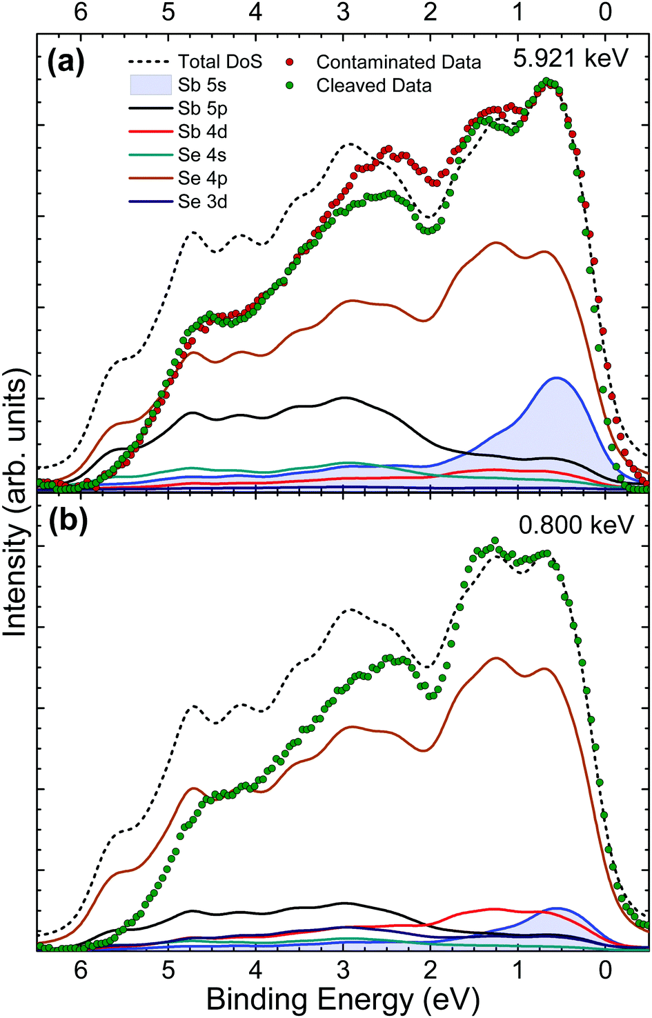 | ||
| Fig. 5 VB XPS spectra from an Sb2Se3 single crystal sample for (a) hard X-rays with a photon energy of 5.921 keV (HAXPES), before and after in situ crystal cleaving; and (b) soft X-rays with a 0.800 keV photon energy after in situ cleaving. Both are plotted with total and partial theoretical VB DoS calculations. | ||
The data from the in situ cleaved crystal agrees well with the theoretically predicted DoS at low binding energies, however the intensities fall off increasingly with binding energy despite replicating the overall shape of the total DoS (black short dashed line) fairly well. This effect is most likely due to final-state relaxation effects which have been observed to shift high binding energy valence band features to lower binding energies.23,24,47 Other possible contributors to this lack of intensity arise from DFT inaccuracies in dealing with the van der Waals bonding present in this material and also the lack of a well established or optimal method for background subtraction of valence band photoemission data. The DoS predicts a large contribution to the spectra from the Sb 5s state at low binding energy which is supported by the strong agreement with the experimental data in this region. This result is significant because it suggests a lone pair of electrons in the Sb 5s state, causing this group V element to be in an Sb(III) oxidation state, instead of the naïvely expected Sb(V) state for a group V element. The presence of this lone pair Sb 5s state contributes to the observed layer-like ribbon structure as summarised by Walsh et al.21
Due to the photoionization cross-section energy dependence (Fig. 2), the cross-section corrected DoS for 0.800 keV in Fig. 5(b) predicts lower relative contributions to the spectra from s orbitals, and additional intensity from d and p orbitals, compared with the calculated cross-section corrected DoS for 5.921 keV in Fig. 5(a). This is consistent with the experimental data, which shows reduced relative intensity in the initial feature near the VB onset, confirming that the Sb 5s lone pair state is in fact occupied and contributing intensity in this region. Strong interaction between the cation s and anion p orbitals results in high-energy anti-bonding states with a considerable degree of cation s character at the top of the upper valence band.21 The hybridization of the Sb 5s states with Se 4p states results in intensity from the Se 4p states also occurring at the VBM. In other words, in the absence of the Sb 5s lone pair states at top of the valence band, the VBM would be lower in energy, further from the vacuum level.
The implications of the presence of stereochemically active lone pairs at the valence band edge has been explored previously, such as the work on the different tin sulfide phases.23,48 The mixing of the p-orbitals with the ns2 lone pair effectively ‘drags’ the valence band edge to a lower binding energy and leads to the phases that possess this lone pair to have a significantly lower band gap and ionization potential than those without. By comparing this work with those results and similar work performed by the same group on CuSbS2,24 it can be seen that the ionization potentials of CuSbS2, SnS and Sn2S3 (the tin sulfide phases possessing a lone pair) range from 4.66 eV to 4.98 eV. However, chalcogenide materials that are similar but lack an ns2 lone pair at the top of the valence band, such as SnS2 and CdS, have ionization potentials ranging from 5.67 eV to 6.70 eV. In order to see how Sb2Se3 fits in with this trend, the ionization potential of an identical crystal as used in the HAXPES was determined. By measuring the valence band edge and secondary electron cut-off (SEC) of the XPS spectrum, as shown in Fig. 6, and using eqn (1) (in which hν is the incident X-ray excitation energy, hν = 1486.6 eV) the ionization potential can be calculated.
| IP = hν − (SEC − VBM) | (1) |
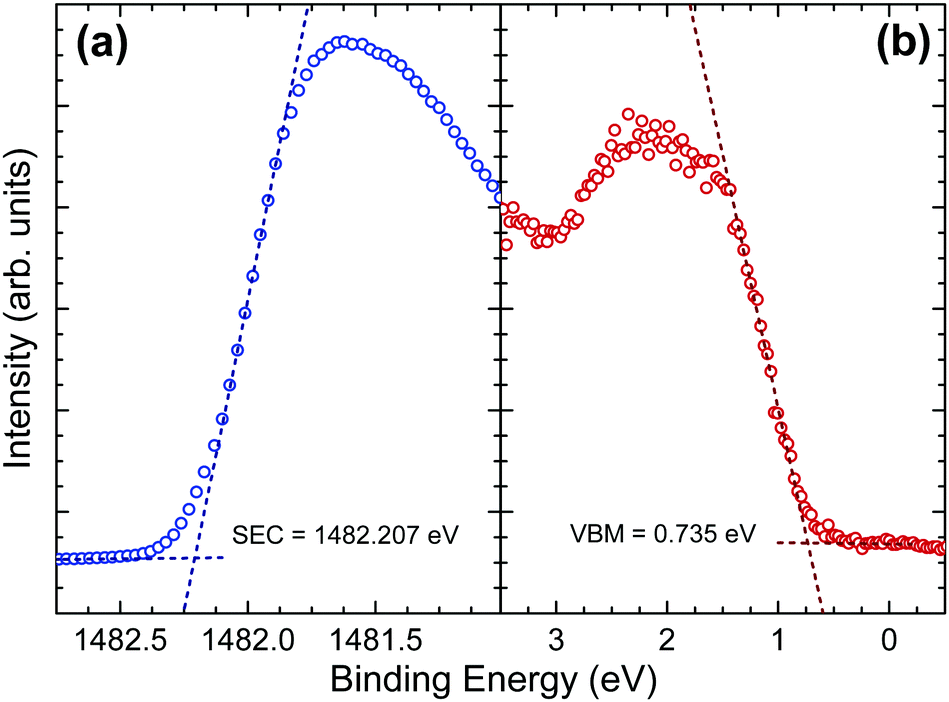 | ||
| Fig. 6 (a) Secondary electron cut-off (blue) and (b) valence band maximum (red) of in situ cleaved Sb2Se3 bulk crystals with straight line fits used to determine the binding energy of the cut-offs. The incident photon energy is 1486.6 eV. | ||
The measured ionization potential for the Sb2Se3 crystal in this study was found to be 5.13 eV. As shown in Fig. 7, this is towards the upper end of the values for other 5s2 lone-pair-containing materials, but certainly well below many of the materials without lone pairs. This demonstrates that not only is understanding the lone pair model important from a structural perspective, but it also affects the electronic properties. In the context of photovoltaics, understanding the dependence of ionization potential on the lone pairs could inform band alignment engineering between absorber and window layers for improving performance of solar cells. For example, based on unfavourable band alignments, CdS has previously been suggested to be a non-optimal solar cell junction partner for SnS (ref. 23 and 51) and CuSbS2 (ref. 24).
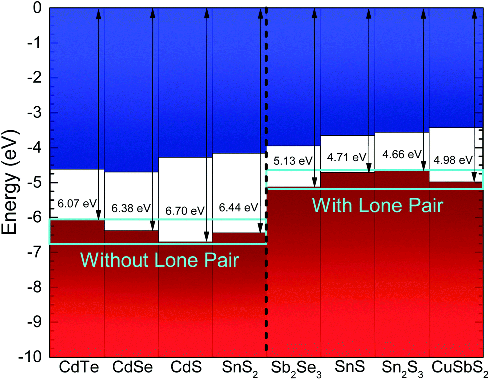 | ||
| Fig. 7 Ionization potential for Sb2Se3 from the photoemission results in Fig. 6, compared with literature values for other materials.23,24,49,50 The zero of the energy scale corresponds to the vacuum level. The materials are labelled as without or with lones pair 5s2 electrons. | ||
4 Conclusion
To better understand the electrical properties, chemical composition and effects of surface contamination on Sb2Se3, high-resolution core-level and valence band photoemission results have been analysed, and the latter has been compared with theoretical calculations. In situ cleaving of an Sb2Se3 crystal, that had been exposed to atmospheric conditions, removes all observed effects from surface oxidation in our core-level HAXPES results, indicating that this exposure does not significantly impact the bulk of the crystal.Using the energy dependence of photoionization cross-sections, shifts in valence band photoemission features have been linked to bonding mechanisms. The agreement observed between the theoretical VB DoS and the experimental photoemission data near the VBM provides strong evidence that Sb2Se3 exhibits contributions to the VB spectra from a lone pair of electrons in the Sb 5s state.
The Sb 5s lone pair states at the top of the valence band are responsible for the relatively high VBM on an absolute energy scale and low ionization potential of 5.13 eV, as measured by XPS. This band alignment has been compared with related materials and will inform future design of Sb2Se3 solar cells and other devices.
Author contributions
The crystals were grown by TDCH under the guidance of KD. The synchrotron photoemission data was collected by HS, LAHJ, JENS, MJS, TJF, PKT and T-LL and analysed by CHD and HS with input from TDV. The XPS data was collected by HS under the guidance of VRD. The DFT calculations were performed and analysed by CNS and DOS. Photovoltaic device-related band alignment insights were provided by JDM and KD. The manuscript was written by CHD, HS and TDV. All authors commented on and edited the manuscript.Conflicts of interest
The authors have no conflicts of interest.Acknowledgements
HS, TDCH, JENS, MJS, LAHJ and TJF acknowledge studentship funding from the Engineering and Physical Sciences Research Council (EPSRC) (EP/L01551X/1, EP/R513271/1). VRD and TDV acknowledge funding from EPSRC grant no. EP/N015800/1 and JDM from Grant No. EP/N014057/1. We acknowledge Diamond Light Source for time on Beamline I09 under Proposal No. SI21431-1. The authors acknowledge the use of the UCL Legion and Grace High Performance Computing Facility (Legion@UCL and Grace@UCL) in the production of computational work. This work was also performed on the ARCHER UK National Supercomputing Service, via our membership of the UK's HEC Materials Chemistry Consortium, funded by EPSRC grants EP/L000202 and EP/R029431. CNS is grateful to the Department of Chemistry at UCL for the provision of a DTA studentship (ref no. 1492829). DOS acknowledges support from the SUPERSOLAR Solar Energy Hub (EP/J017361/1) and EPSRC grant EP/N01572X/1. DOS and TDV acknowledge membership of the Materials Design Network.References
- X. Wang, R. Tang, C. Wu, C. Zhu and T. Chen, J. Energy Chem., 2018, 27, 713–721 CrossRef.
- K. Momma and F. Izumi, J. Appl. Crystallogr., 2011, 44, 1272–1276 CrossRef.
- Y. Zhou, M. Leng, Z. Xia, J. Zhong, H. Song, X. Liu, B. Yang, J. Zhang, J. Chen, K. Zhou, J. Han, Y. Cheng and J. Tang, Adv. Energy Mater., 2014, 4, 1301846 CrossRef.
- H. El-Shair, A. Ibrahim, E. A. El-Wahabb, M. Afify and F. A. El-Salam, Vacuum, 1991, 42, 911–914 CrossRef.
- R. R. Prabhakar, W. Septina, S. Siol, T. Moehl, R. Wick-Joliat and S. D. Tilley, J. Mater. Chem. A, 2017, 5, 23139–23145 RSC.
- L. Zhang, Y. Li, C. Li, Q. Chen, Z. Zhen, X. Jiang, M. Zhong, F. Zhang and H. Zhu, ACS Nano, 2017, 11, 12753–12763 CrossRef PubMed.
- W. Yang, J. H. Kim, O. S. Hutter, L. J. Phillips, J. Tan, J. Park, H. Lee, J. Major and J. S. Lee, Nat. Commun., 2020, 11, 861 CrossRef PubMed.
- M. Birkett, W. M. Linhart, J. Stoner, L. J. Phillips, K. Durose, J. Alaria, J. D. Major, R. Kudrawiec and T. D. Veal, APL Mater., 2018, 6, 084901 CrossRef.
- Z. Li, X. Liang, G. Li, H. Liu, H. Zhang, J. Guo, J. Chen, K. Shen, X. San, W. Yu, R. E. I. Schropp and Y. Mai, Nat. Commun., 2019, 10, 125 CrossRef PubMed.
- X. Liu, J. Chen, M. Luo, M. Leng, Z. Xia, Y. Zhou, S. Qin, D.-J. Xue, L. Lv, H. Huang, D. Niu and J. Tang, ACS Appl. Mater. Interfaces, 2014, 6, 10687–10695 CrossRef PubMed.
- C. Chen, L. Wang, L. Gao, D. Nam, D. Li, K. Li, Y. Zhao, C. Ge, H. Cheong, H. Liu, J. Song and H. Tang, ACS Energy Lett., 2017, 2, 2125–2132 CrossRef.
- O. S. Hutter, L. J. Phillips, K. Durose and J. Major, Sol. Energy Mater. Sol. Cells, 2018, 188, 177–181 CrossRef.
- H. Shiel, O. Hutter, L. Phillips, M. Al Turkestani, V. R. Dhanak, T. D. Veal, K. Durose and J. D. Major, J. Phys. Energy, 2019, 1, 045001 CrossRef.
- D.-B. Li, X. Yin, C. R. Grice, L. Guan, Z. Song, C. Wang, C. Chen, K. Li, A. J. Cimaroli, R. A. Awni, D. Zhao, H. Song, W. Tang, Y. Yan and J. Tang, Nano Energy, 2018, 49, 346–353 CrossRef CAS.
- R. E. Williams, Q. M. Ramasse, K. P. McKenna, L. J. Phillips, P. J. Yates, O. S. Hutter, K. Durose, J. D. Major and B. G. Mendis, ACS Appl. Mater. Interfaces, 2020, 12, 21730–21738 CrossRef CAS.
- J. Tao, X. Hu, Y. Guo, J. Hong, K. Li, J. Jiang, S. Chen, C. Jing, F. Yue, P. Yang, C. Zhang, Z. Wu, J. Tang and J. Chu, Nano Energy, 2019, 60, 802–809 CrossRef CAS.
- K. Li, S. Wang, C. Chen, R. Kondrotas, M. Hu, S. Lu, C. Wang, W. Chen and J. Tang, J. Mater. Chem. A, 2019, 7, 9665–9672 RSC.
- X. Wen, C. Chen, S. Lu, K. Li, R. Kondrotas, Y. Zhao, W. Chen, L. Gao, C. Wang, J. Zhang, G. Niu and J. Tang, Nat. Commun., 2018, 2018, 2179 CrossRef PubMed.
- K. Shen, Y. Zhang, X. Wang, C. Ou, F. Guo, H. Zhu, C. Liu, Y. Gao, R. Schropp, Z. Li, X. Liu and Y. Mai, Adv. Sci., 2020, 2001013 CrossRef PubMed.
- Y. Zhou, L. Wang, S. Chen, S. Qin, X. Liu, J. Chen, D.-J. Xue, M. Luo, Y. Cao, Y. Cheng, E. H. Sargent and J. Tang, Nat. Photonics, 2015, 9, 409 CrossRef CAS.
- A. Walsh, D. J. Payne, R. G. Egdell and G. W. Watson, Chem. Soc. Rev., 2011, 40, 4455–4463 RSC.
- J. J. Carey, D. O. Allen, J. P. Scanlon and G. W. Watson, J. Solid State Chem., 2014, 213, 116–125 CrossRef CAS.
- T. J. Whittles, L. A. Burton, J. M. Skelton, A. Walsh, T. D. Veal and V. R. Dhanak, Chem. Mater., 2016, 28, 3718–3726 CrossRef CAS.
- T. J. Whittles, T. D. Veal, C. N. Savory, A. W. Welch, F. W. S. Lucas, J. T. Gibbon, M. Birkett, R. J. Potter, D. O. Scanlon, A. Zakutayev and V. R. Dhanak, ACS Appl. Mater. Interfaces, 2017, 9, 41916–41926 CrossRef CAS.
- J. H. Scofield, Theoretical photoionization cross sections from 1 to 1500 keV, California Univ., Livermore, Lawrence Livermore Lab., technical report, 1973.
- L. Wang, D.-B. Li, K. Li, C. Chen, H.-X. Deng, L. Gao, Y. Zhao, F. Jiang, L. Li and F. Huang, et al. , Nat. Energy, 2017, 2, 17046 CrossRef CAS.
- C. Chen, Y. Zhao, S. Lu, K. Li, Y. Li, B. Yang, W. Chen, L. Wang, D. Li and H. Deng, et al. , Adv. Energy Mater., 2017, 7, 1700866 CrossRef.
- R. J. Mehta, C. Karthik, W. Jiang, B. Singh, Y. Shi, R. W. Siegel, T. Borca-Tasciuc and G. Ramanath, Nano Lett., 2010, 10, 4417–4422 CrossRef CAS.
- J. F. Moulder, W. F. Stickle, P. E. Sobol and K. D. Bomben, Handbook of X-ray Photoelectron Spectroscopy, PerkinElmer Corporation, 1992, p. 261 Search PubMed.
- N. Fleck, T. D. C. Hobson, C. N. Savory, J. Buckeridge, T. D. Veal, M. R. Correia, D. O. Scanlon, K. Durose and F. Jäckel, J. Mater. Chem. A, 2020, 8, 8337–8344 RSC.
- T. D. C. Hobson, L. J. Phillips, O. S. Hutter, H. Shiel, J. E. N. Swallow, C. N. Savory, P. K. Nayak, S. Mariotti, B. Das, L. Bowen, L. A. H. Jones, T. J. Featherstone, M. J. Smiles, M. A. Farnworth, G. Zoppi, P. K. Thakur, T.-L. Lee, H. J. Snaith, C. Leighton, D. O. Scanlon, V. R. Dhanak, K. Durose, T. D. Veal and J. D. Major, Chem. Mater., 2020, 32, 2621–2630 CrossRef CAS.
- T. D. C. Hobson, O. S. Hutter, M. Birkett, T. D. Veal and K. Durose, 2018 IEEE 7th World Conference on Photovoltaic Energy Conversion (WCPEC) (A Joint Conference of 45th IEEE PVSC, 28th PVSEC & 34th EU PVSEC), 2018, 0818–0822.
- H. Song, T. Li, J. Zhang, Y. Zhou, J. Luo, C. Chen, B. Yang, C. Ge, Y. Wu and J. Tang, Adv. Mater., 2017, 29, 1700441 CrossRef PubMed.
- D. A. Shirley, Phys. Rev. B: Solid State, 1972, 5, 4709–4714 CrossRef.
- G. Kresse and J. Hafner, Phys. Rev. B: Condens. Matter Mater. Phys., 1993, 47, 558–561 CrossRef CAS.
- G. Kresse and J. Hafner, Phys. Rev. B: Condens. Matter Mater. Phys., 1994, 49, 14251–14269 CrossRef CAS PubMed.
- G. Kresse and J. Furthmüller, Phys. Rev. B: Condens. Matter Mater. Phys., 1996, 54, 11169–11186 CrossRef CAS PubMed.
- G. Kresse and J. Furthmüller, Comput. Mater. Sci., 1996, 6, 15–50 CrossRef CAS.
- A. V. Krukau, O. A. Vydrov, A. F. Izmaylov and G. E. Scuseria, J. Chem. Phys., 2006, 125, 224106 CrossRef.
- S. Grimme, J. Comput. Chem., 2004, 25, 1463–1473 CrossRef CAS.
- C. N. Savory and D. O. Scanlon, J. Mater. Chem. A, 2019, 7, 10739–10744 RSC.
- W. Jianqi, F. Daming, W. Wenhui, Z. Minxiu and L. Yiz, Polym. Degrad. Stab., 1991, 31, 129–140 CrossRef.
- R. Delobel, H. Baussart, J.-M. Leroy, J. Grimblot and L. Gengembre, J. Chem. Soc., Faraday Trans. 1, 1983, 79, 879–891 RSC.
- C. D. Wagner, D. A. Zatko and R. H. Raymond, Anal. Chem., 1980, 52, 1445–1451 CrossRef CAS.
- H. Iwakuro, C. Tatsuyama and S. Ichimura, Jpn. J. Appl. Phys., 1982, 21, 94 CrossRef CAS.
- M. Shenasa, S. Sainkar and D. Lichtman, J. Electron Spectrosc. Relat. Phenom., 1986, 40, 329–337 CrossRef CAS.
- L. Ley, R. A. Pollak, F. R. McFeely, S. P. Kowalczyk and D. A. Shirley, Phys. Rev. B: Solid State, 1974, 9, 600 CrossRef CAS.
- L. A. H. Jones, W. M. Linhart, N. Fleck, J. E. N. Swallow, P. A. E. Murgatroyd, H. Shiel, T. J. Featherstone, M. J. S. Smiles, P. K. Thakur, T.-L. Lee, L. J. Hardwick, J. Alaria, F. Jäckel, R. Kudrawiec, L. A. Burton, A. Walsh, J. M. Skelton, T. D. Veal and V. R. Dhanak, Phys. Rev. Mater., 2020, 4, 074602 CrossRef CAS.
- J. D. Major, L. J. Phillips, M. Al Turkestani, L. Bowen, T. J. Whittles, V. R. Dhanak and K. Durose, Sol. Energy Mater. Sol. Cells, 2017, 172, 1–10 CrossRef CAS.
- V. Stevanović, S. Lany, D. S. Ginley, W. Tumas and A. Zunger, Phys. Chem. Chem. Phys., 2014, 16, 3706–3714 RSC.
- L. A. Burton and A. Walsh, Appl. Phys. Lett., 2013, 102, 132111 CrossRef.
Footnotes |
| † Electronic supplementary information (ESI) available: SEM image and EDX spectrum, indicating Sb and Se weight and atomic percentages. Survey HAXPES spectrum, illustrating the plasmon loss feature at a binding energy of 17.9 eV higher than each core level peak. See DOI: 10.1039/d0tc03470c |
| ‡ Contributed equally to this work. |
| This journal is © The Royal Society of Chemistry 2020 |