DOI:
10.1039/D2TC02144G
(Paper)
J. Mater. Chem. C, 2022,
10, 10888-10894
Highly sensitive broadband photomultiplication type all-polymer photodetectors and their applications in optical pulse counting†
Received
24th May 2022
, Accepted 7th July 2022
First published on 7th July 2022
1. Introduction
Polymer photodetectors (PPDs) present a remarkable commercial potential due to the typical characteristics of flexibility and eco-friendliness.1–3 Photomultiplication type PPDs (PM-PPDs) have emerged as the research hotspot in recent years, exhibiting the prominent advantages such as high-sensitivity, low-power consumption and tunable spectral-response-range.4–6 PM-PPDs can be obtained on the basis of active layers possessing single charge carrier transport channels, which were firstly reported by Zhang's group.7–9 The weight difference between the donor and the acceptor is dozens of times in active layers of PM-PPDs, which prefer to form some isolated traps for one kind of charge and also retain continuous transport channels for the opposite charge. The interfacially trapped-charge can produce a Coulomb-force to cause enough interfacial band-bending for opposite charge tunneling-injection into active layers, generating considerable light current density (JL) of PM-PPDs. The PM phenomenon with external-quantum-efficiency (EQE) higher than unity is achieved with the number of charge traversing the active layers being more than that of incident photons per unit-time.10 EQE values of PM-PPDs could be increased by the means of optimizing the charge tunneling-injection as well as the charge-transport in the active layers.11,12 The EQE of PM-PPDs is tripled by incorporating a transparent hole-transporting polymer into active layers, resulting from the simultaneously improved hole tunneling-injection and transport in active layers.13 Charge injection barrier is one of key factors that control charge tunneling-injection, which can be adjusted by employing an electrode modification layer.14 Miao et al. employed PFN as the ITO modification layer to fabricate PM-PPDs based on the configuration of ITO/PFN/active layer/Al, which can work well under both forward and reverse applied bias due to the optimized hole injection barrier.15 Recently, Chung et al. employed PFN-Br as the interfacial layer to modify the ITO work function, leading to the further improved EQE values of P3HT![[thin space (1/6-em)]](https://www.rsc.org/images/entities/char_2009.gif) :PCBM (100:1, wt/wt) based PM-PPDs under forward applied bias because of the decreased charge injection barrier.16 Meanwhile, the spectral-response-range of PM-PPDs could be altered via adjusting the distribution of trapped-charge in the vicinity of the opposite charge injection electrode.17 Narrowband PM-PPDs could be obtained by applying the charge injection narrowing (CIN) concept, which can retain the narrowband response characteristic under a large applied bias.12 The near-infrared (NIR) narrowband PM-PPDs based on the CIN concept exhibit a full-width-at-half-maximum narrower than 30 nm and EQE of over 15300% at 850 nm under −13 V applied bias, which were prepared using 3 μm-thick active layers based on P3HT:PTB7-Th:BEH (100:0.5:3, wt/wt/wt).18 Many efforts have been devoted to preparing broadband PM-PPDs, such as ternary strategy and double-layered scheme.19–23 Ternary strategy is usually utilized to expand the absorption spectra of active layers via incorporating narrow bandgap materials as the third component,19,20 leading to an extended spectral response of PM-PPDs.21,22 The broadband PM-PPDs based on the double-layered scheme contain an absorber layer to cover a wide spectral range and a multiplication layer to achieve EQEs greater than 100%. The broadband PM-PPDs can be fabricated via PM6:Y6 (1:1.5, wt/wt) acting as an absorber layer and P3HT:PC71BM (5:100, wt/wt) acting as a multiplication layer, exhibiting a broad spectral response covering the ultraviolet (UV) to the NIR range with a peak EQE value of 1200% under a 10 V applied bias.23 The absorption spectral range of active layers can be further extended with the development of narrow bandgap materials,24,25 which is conducive to preparing high-performance broadband PM-PPDs.26,27 It's challenging to concurrently achieve broad spectral response and relatively large EQE values of PM-PPDs, especially under a small applied bias.
:PCBM (100:1, wt/wt) based PM-PPDs under forward applied bias because of the decreased charge injection barrier.16 Meanwhile, the spectral-response-range of PM-PPDs could be altered via adjusting the distribution of trapped-charge in the vicinity of the opposite charge injection electrode.17 Narrowband PM-PPDs could be obtained by applying the charge injection narrowing (CIN) concept, which can retain the narrowband response characteristic under a large applied bias.12 The near-infrared (NIR) narrowband PM-PPDs based on the CIN concept exhibit a full-width-at-half-maximum narrower than 30 nm and EQE of over 15300% at 850 nm under −13 V applied bias, which were prepared using 3 μm-thick active layers based on P3HT:PTB7-Th:BEH (100:0.5:3, wt/wt/wt).18 Many efforts have been devoted to preparing broadband PM-PPDs, such as ternary strategy and double-layered scheme.19–23 Ternary strategy is usually utilized to expand the absorption spectra of active layers via incorporating narrow bandgap materials as the third component,19,20 leading to an extended spectral response of PM-PPDs.21,22 The broadband PM-PPDs based on the double-layered scheme contain an absorber layer to cover a wide spectral range and a multiplication layer to achieve EQEs greater than 100%. The broadband PM-PPDs can be fabricated via PM6:Y6 (1:1.5, wt/wt) acting as an absorber layer and P3HT:PC71BM (5:100, wt/wt) acting as a multiplication layer, exhibiting a broad spectral response covering the ultraviolet (UV) to the NIR range with a peak EQE value of 1200% under a 10 V applied bias.23 The absorption spectral range of active layers can be further extended with the development of narrow bandgap materials,24,25 which is conducive to preparing high-performance broadband PM-PPDs.26,27 It's challenging to concurrently achieve broad spectral response and relatively large EQE values of PM-PPDs, especially under a small applied bias.
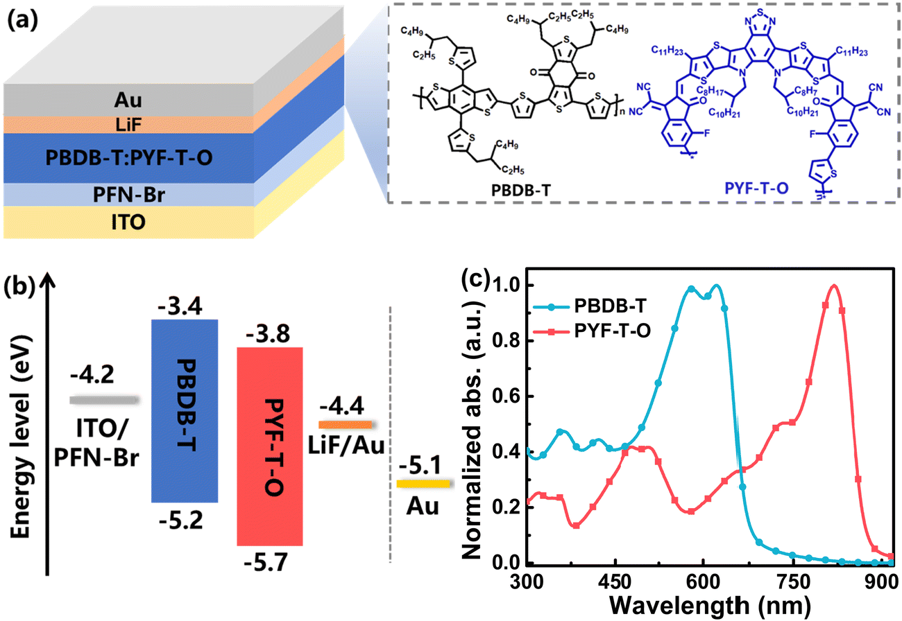
Here, broadband PM type all-polymer photodetectors (PM-APDs) are realized with the active layers containing wide bandgap polymer PBDB-T as the donor and narrow bandgap polymer PYF-T-o as the acceptor.28,29 The device configuration diagram of PM-APDs as well as the chemical structural formulas of polymer PBDB-T and PYF-T-o are depicted in Fig. 1a. The incorporation weight ratio between PBDB-T and PYF-T-o is kept constant at 3:100 in active layers. Hole traps could be formed with rather small amounts of PBDB-T encircled by PYF-T-o due to the 0.5 eV level difference between the highest occupied molecular orbitals (HOMOs). The energy level alignments of materials used in the PM-APDs are sketched in Fig. 1b. The trapped-holes at the vicinity of the Au electrode can produce a Coulomb-force to cause interfacial band-bending for electron tunneling-injection, leading to the PM phenomenon with EQE values higher than 100%. The PM-APDs exhibit a broad spectral response covering 310–900 nm, benefitting from the wide photon harvest range of polymers PBDB-T and PYF-T-o, as shown in Fig. 1c. The performance of PM-APDs is improved via decreasing the active layer thickness to 160 nm, benefiting from the improved electron tunneling-injection and collection. An ultrathin (1 nm) LiF layer was selected as the interfacial layer to decrease the electron injection barrier, leading to the markedly improved EQE values from 600% to 18000% at 360 nm and from 300% to 9000% at 850 nm under 4 V applied bias. The PM-APDs with the LiF layer can achieve high EQE values under small forward applied bias, exhibiting the advantage of low power-consumption. PM-APDs with the LiF layer exhibit a specific detectivity (D*) greater than 1.0 × 10¹² Jones in the spectral-response-range of 310–900 nm under 4 V applied bias, which are successfully applied in an optical pulse counting circuit due to the sensitive photodetection capability.
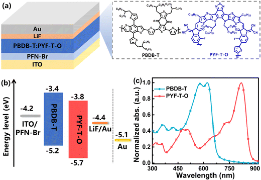 |
| | Fig. 1 (a) Device configuration schematic of PM-APDs, chemical structural formulas of PBDB-T and PYF-T-o. (b) Energy level alignments of materials employed in PM-APDs. (c) Absorption spectra of PBDB-T and PYF-T-o neat films. | |
2. Results and discussion
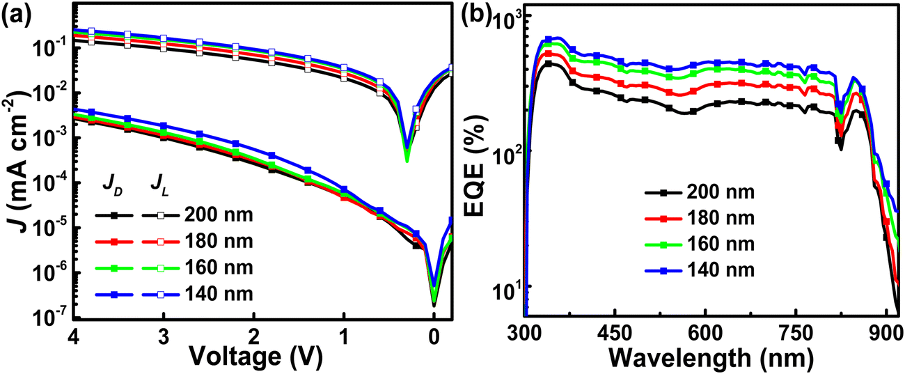
A set of PM-APDs were prepared with ITO/PFN-Br/PBDB-T:PYF-T-o (3:100, wt/wt)/Au as the configuration based on different active layer thicknesses. The current density (J)–voltage (V) curves of all the PM-APDs were tested under the conditions of darkness or white light-illumination with the intensity of 1 mW cm−2, as displayed in Fig. 2a. The JL values of PM-APDs are far larger than the dark current density (JD) values under the identical forward applied bias, which should originate from electron tunneling-injection assisted by the trapped-holes in the vicinity of the Au electrode under light illumination conditions. To intuitively describe the operation principle of PM-APDs, the schematics of charge injection and transport process are sketched in Fig. S1 (ESI†). Both electrons and holes are hardly injected into the active layers under forward applied bias due to the large injection barriers of 1.3 eV for electrons and 1.0 eV for holes. Meanwhile, hole-transport is hindered because of the lack of hole-transport channels in active layers containing rather low PBDB-T content. The rather low JD of PM-APDs mainly results from the blocked charge injection and limited hole-transport in the active layers. Photogenerated holes in active layers may prefer to be trapped in PBDB-T encircled by PYF-T-o under light-illumination. The trapped-holes in the vicinity of the Au electrode can produce Coulomb-force to cause enough interfacial band-bending for efficient electron tunneling-injection from the Au electrode into active layers. Tunneling-injected electrons are effectively transported along the channels formed by PYF-T-o and then collected by the ITO electrode under a forward applied bias, leading to the large JL of PM-APDs. The JL values of PM-APDs are increased by decreasing active layer thickness, resulting from the simultaneously optimized electron tunneling-injection and collection by the ITO electrode. The density of trapped-holes in the vicinity of the Au electrode can be improved due to the more photon transmission to a nearby Au electrode with the decrement of the active layer thickness,30,31 resulting in the enhanced electron tunneling-injection. More tunneling-injected electrons could be effectively collected by the ITO electrode, benefiting from the shortened electron-transport distance in thin active layers.
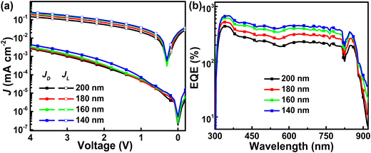 |
| | Fig. 2 (a) J–V curves and (b) EQE spectra under 4 V applied bias of PM-APDs. | |
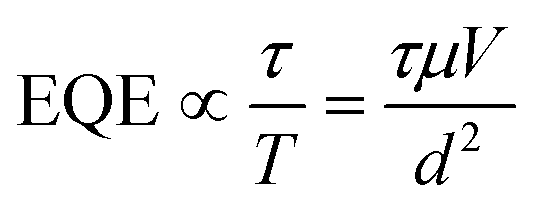
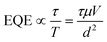
The EQE spectra of PM-APDs were explored under a 4 V applied bias, displayed in Fig. 2b. The EQE values of all the PM-APDs are much larger than unity in the entire spectral-response range. The EQE values of PM-APDs are increased by decreasing active layer thickness, resulting from the increased number of tunneling-injected electrons traversing active layers per unit-time. The EQE of PM-APDs can also be estimated from the formula32
| |  | (1) |
where
τ is lifetime of trapped-holes,
μ is electron mobility in the active layers,
V is applied bias,
T is time for tunneling-injected electrons transporting in the active layers, and
d is active layer thickness. The transporting time of tunneling-injected electrons could be shortened
via decreasing the thickness of active layers, leading to the improved EQE of PM-APDs. PM-APDs exhibit a broad spectral response covering 310–900 nm, resulting from the wide trapped-hole distribution in the vicinity of Au electrode. There is an apparent EQE spectral dip at 825 nm of all PM-APDs, well corresponding to the emission peak of the xenon lamp, as shown in Fig. S2 (ESI
†). It can be envisaged that hole traps could be rapidly filled by photogenerated holes under a strong light-illumination. Redundant photogenerated holes will be recombined by the tunneling-injected electrons, leading to weakened EQE values of PM-APDs. The experimental phenomenon has already been referred to in previous works on PM-APDs.
23,33,34 To further explore the active layer thickness on the performance of PM-APDs, the responsivity (
R) and
D* of PM-APDs with different active layer thickness were investigated under a 4 V applied bias and are shown in Fig. S3a and b (ESI
†).
R values of photodetectors can be obtained by the following equation:
| |  | (2) |
in which
λ is incident light wavelength. The
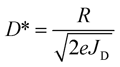
D* was estimated using
JD according to the equation
| |  | (3) |
where
e is the elementary charge. The
R values of PM-APDs are increased with the decrement of the active layer thickness, which is consistent with the increasing trend of EQE dependence on the active layer thickness due to the proportional relationship between the
R and EQE. The
D* values of PM-APDs are improved and then slightly declined with the decreased active layer thickness, which mainly resulted from the variation of
JD and
JL with active layer thickness. The improved
D* values of PM-APDs should primarily benefit from the increased
JL and negligible increment of
JD with the active layer thickness decreased from 200 to 160 nm. The
JD is obviously increased with the active layer thickness decreased to 140 nm, leading to the slightly declined
D* values of PM-APDs. The optimal active layer thickness of PM-APDs is about 160 nm for achieving considerable EQE and
R values, also obtaining the optimized
D* values.
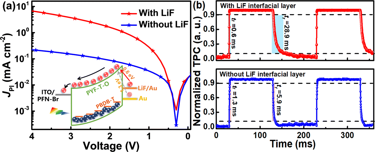
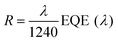
The injection barrier plays a critical role in determining charge tunneling-injection for PM-APDs.35 The performance of PM-APDs could be further optimized via enhancing electron tunneling-injection under light-illumination. The ultrathin (∼1 nm) LiF layer acts as an interfacial layer to modify the work function of the Au electrode. The work functions of Au and LiF/Au are commonly reported as about −5.1 eV and −4.4 eV, respectively.36 The electron injection barrier can be markedly decreased by inserting the LiF layer under forward applied bias.37,38 The J–V curves of PM-APDs with 1 nm LiF as the interfacial layer were tested in the dark and under white light-illumination with the intensity of 1 mW cm−2, shown in Fig. S4 (ESI†). The JL and JD values of PM-APDs with the LiF layer are simultaneously improved in contrast to those of PM-APDs without the LiF layer, resulting from the decreased electron injection barrier under a forward applied bias. The photoinduced-current density (JPI) of PM-APDs can be obtained from JL subtracted JD.39 The JPI–V curves of PM-APDs with or without the LiF layer are plotted as Fig. 3a. The JPI of PM-APDs can be markedly improved from 0.2 to 6.7 mA cm−2 under 4 V applied bias by employing the LiF layer, owing to the markedly decreased electron injection barrier from 1.3 to 0.6 eV. To further explore the influence of the LiF layer on the PM-APD performance, the normalized transient photocurrent (TPC) of PM-APDs with or without the LiF layer was obtained at 850 nm light-illumination with an intensity of 1 mW cm−2 under a 4 V applied bias, plotted in Fig. 3b. The rising time (tr) and falling time (tf) could be acquired from the normalized TPC, which represent the response-speed of PM-APDs when the incident light is switched on or off. The tr (tf) is the time period for photocurrent varying from 10% (90%) to 90% (10%) of maximal values, respectively.40,41 The tr of PM-APDs mainly comprises the time of accumulating enough trapped-holes near the Au electrode to induce efficient interfacial band-bending for electron tunneling-injection and the time of electron-transport in active layers. The tf of PM-APDs mainly depends on the time for the trapped-holes to be released from traps and collected by the Au electrode or recombined with the injected electrons from the external circuit. The tr and tf are individually 0.6 and 28.9 ms for PM-APDs with the LiF layer, 1.3 and 5.9 ms for PM-APDs without the LiF layer. The PM-APDs evince a relatively rapid response-speed when the incident light is switched on, because the hole traps at the vicinity of the LiF/Au or the Au electrode can be rapidly filled to cause interfacial band-bending for efficient electron tunneling-injection. The response-speed of PM-APDs is relatively slow when the incident light is switched off, because the trapped-holes will undergo a slow release process from traps or recombined with the tunneling-injected electrons. The response-speed of PM-APDs could be improved by employing the LiF layer when the incident light is switched on, primarily resulting from efficient electron tunneling-injection with the lower injection barrier from LiF/Au onto the lowest unoccupied molecular orbital (LUMO) of PYF-T-o. The electron injection barrier is decreased from 1.3 to 0.6 eV by inserting LiF layer, leading to a more rapid electron tunneling-injection under a forward applied bias. The response-speed of PM-APDs becomes slower by employing an LiF layer when the incident light is switched off, resulting from the suppressed collection of released holes from the traps by the LiF layer under a forward applied bias. Part of released holes remain in the active layer and still assist electron tunneling-injection although the incident light is switched off, leading to the slower decaying process of tf for the PM-APDs with the LiF layer.
 |
| | Fig. 3 PM-APDs with or without LiF layer: (a) JPI–V curves, the inset depicts the effect of electron injection barrier on electron tunneling-injection. (b) Normalized TPC obtained at 850 nm light-illumination with the intensity of 1 mW cm−2 under 4 V applied bias. | |
To further estimate the performance of the optimal PM-APDs with the LiF layer, the EQE spectra were investigated under different forward applied biases, shown as Fig. 4a. The EQE values of optimal PM-APDs are increased by raising the forward applied bias, which should be on account of the optimized electron tunneling-injection and electron-transport in active layers under a large applied bias.34,42 The EQE values of the optimal PM-APDs are increased from 1000% to 18000% at 360 nm and from 500% to 9000% at 850 nm with a forward applied bias increased from 1 to 4 V, which are much larger than 600% at 360 nm and 300% at 850 nm for the PM-APDs without the LiF layer under a 4 V applied bias. The markedly improved EQE values of PM-APDs with the LiF layer mainly benefit from the enhanced electron tunneling-injection under the increased forward applied bias, which can be explained via two aspects: (i) The trapped-hole density near the Au electrode will be improved with more photogenerated holes transported towards the Au electrode under a high forward applied bias, assisting more electrons being tunneling-injected into active layers. (ii) The interfacial band will become more tilted along with the increased forward applied bias, leading to the narrowed electron injection barrier. More electrons can be easily tunneling-injected into active layers due to the narrowed injection barrier under a high forward applied bias. R is a critical parameter for estimating the photoelectric response ability of photodetectors.43 The R spectra of the optimal PM-APDs under different forward applied bias are exhibited in Fig. 4b. The optimal PM-APDs exhibit the R values of 54.4 A W−1 at 360 nm and 64.6 A W-−1 at 850 nm under a 4 V applied bias, displaying the good photoelectric response performance.44D* is the figure of merit to represent the capability of photodetectors detecting weak optical signals, which could be calculated from the following equation:45
| |  | (4) |
where
A is active area,
B is the measured electrical bandwidth,
in is total noise current. The
D* spectrum of optimal PM-APDs was investigated by employing
in under a 4 V applied bias, presented in
Fig. 4c. The
in of optimal PM-APDs was measured as shown in the inset of
Fig. 4c, which is 2.4 × 10
−11 A Hz
−1/2 at 70 Hz under a 4 V applied bias.
D* values of optimal PM-APDs are 3.6 × 10
12 Jones at 360 nm and 4.2 × 10
12 Jones at 850 nm, indicating the sensitive photodetection capability of optimal PM-APDs. The
R and
D* of PM-APDs with the LiF layer were investigated under 850 nm incident light illumination with different intensities under a 4 V applied bias, as summarized in Table S1 (ESI
†). The
R and
D* of PM-APDs with the LiF layer are improved with decreased incident light intensity, indicating the excellent detection sensitivity in weak light. The stability of optimal PM-APDs was explored under the condition of storage in a nitrogen-filled glove box without any encapsulation. The EQE values of optimal PM-APDs at 360 and 850 nm under a 4 V applied bias dependent on the exposure time are plotted in
Fig. 4d, which are maintained at about 90% of the initial EQE values after being exposed for 120 h. The good stability of optimal PM-APDs benefits from the stable morphology of all-polymer active layers with strong interchain packing.
46–48 The optimal PM-APDs exhibit excellent photoelectric response capability, weak light detection capability and stability, which should have potential applications in practical photoelectric detection.
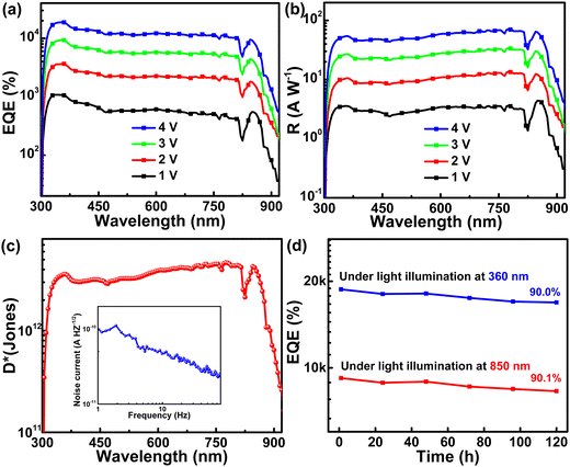 |
| | Fig. 4 Optimal PM-APDs: (a) EQE and (b) R spectra under different forward applied biases. (c) D* spectrum and noise current under a 4 V applied bias. (d) EQE values at 360 and 850 nm under a 4 V applied bias dependent on the exposure time in a nitrogen-filled glove box. | |
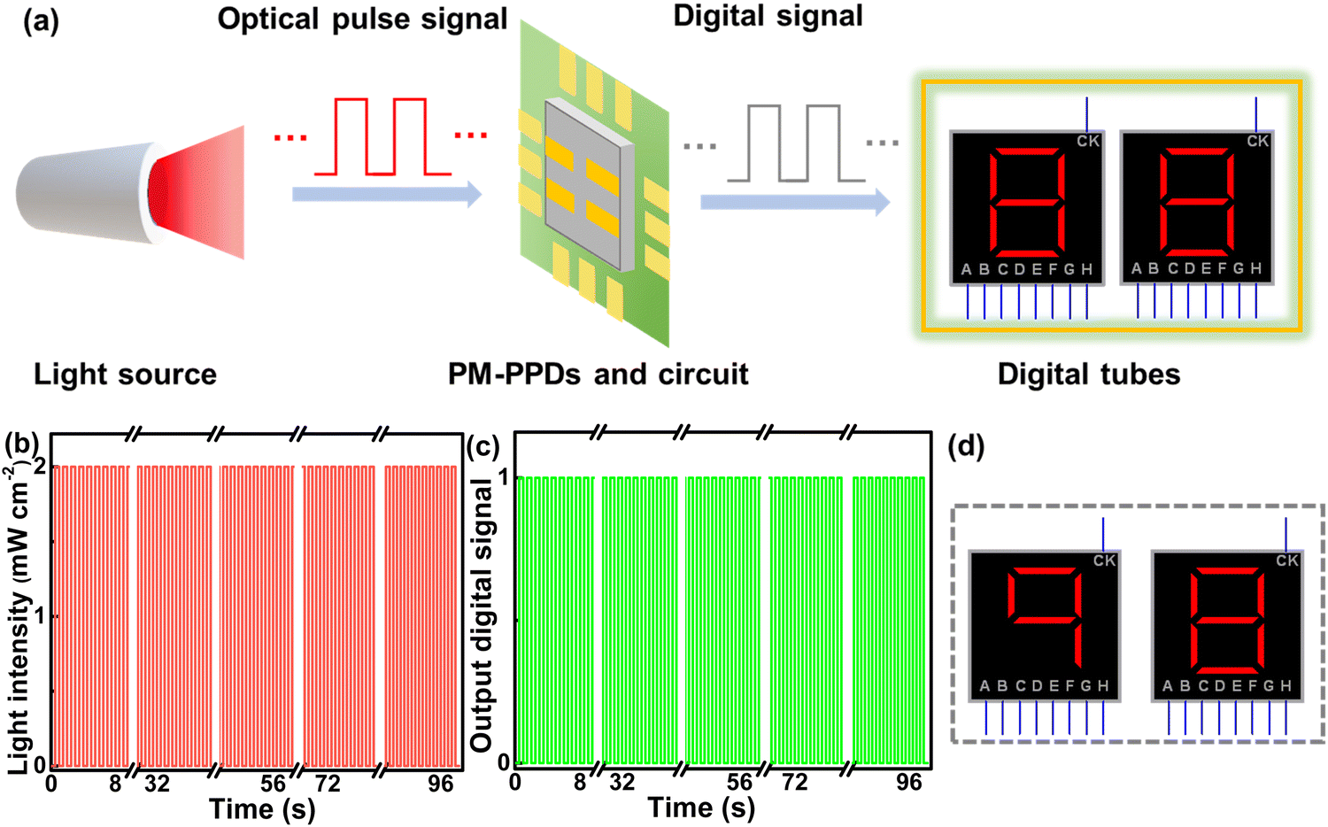
The optimal PM-APDs are applied as optical sensors in an optical pulse counting circuit to demonstrate the feasibility in practical application. The working process of the optimal PM-APD based optical pulse counting circuit is depicted in Fig. 5a. The optical pulse signals are provided by light-emitting-diodes (LEDs), which can be converted into digital electronic signals by the optimal PM-APD based circuit. The digital tubes are driven via digital electronic signals to display the number of input optical pulses. The photograph of the optical pulse counting circuit and detailed circuit diagram are exhibited in Fig. S5a and b (ESI†). LEDs provide the input optical pulse signals at the wavelength of 630 nm with maximum intensity of 2 mW cm−2, as shown in Fig. 5b, which can be converted into a pulse current by the optimal PM-APDs. The current flows through the resistance R0 to induce the variation of the potential at point A. When the potential at point A is higher or lower than the reference voltage, high or low voltage levels of digital electronic signals will be output by the voltage comparator LM393 as exhibited in Fig. 5c. The rising edges of digital electronic signals trigger the counter CD4518 to record the number of received rising edges, which is just the number of input optical pulses. The counter CD4518 commands the decoder CD4511 to drive the seven segment digital tubes for displaying the number of input optical pulses. As shown in Fig. 5d, the readings on digital tubes are exactly the number of input optical pulses. The optical pulse counting circuit can accurately count the number of incident optical pulses and display the number on the digital tubes, as recorded in Movie S1 (ESI†). The optimal PM-APDs operate well in the optical pulse counting circuit, demonstrating sensitive photodetection capability and potential application in the fields of laser ranging, automatic control and biosensing.
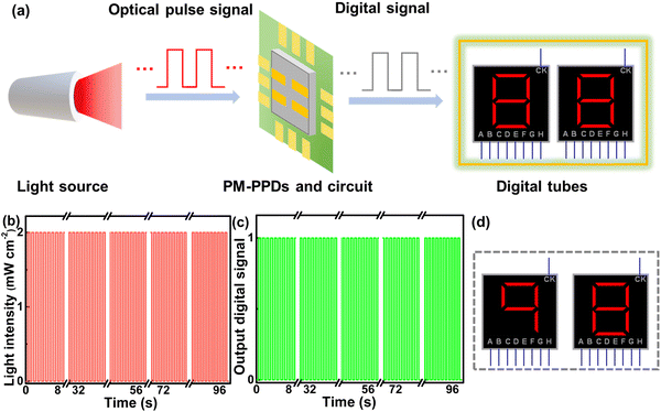 |
| | Fig. 5 (a) Schematic of optical pulse counting circuit based on optimal PM-APDs. (b) Optical pulse signals provided by LEDs and (c) the corresponding digital signals generated by optimal PM-APDs coupled with voltage comparator LM393. (d) Readings displayed on digital tubes. | |
3. Conclusions
The broadband PM-APDs were achieved with the configuration of ITO/PFN-Br/PBDB-T:PYF-T-o (3:100, wt/wt)/LiF/Au, exhibiting a broad spectral response covering 310–900 nm. The operation principle of PM-APDs is based on electron tunneling-injection assisted by trapped-holes in the vicinity of Au electrode. The performance of PM-APDs is improved by decreasing the active layer thickness to 160 nm, resulting from the optimized electron tunneling-injection, transport and collection. The EQE values of PM-APDs are improved by more than one magnitude by employing the LiF layer, benefitting from the enhanced electron tunneling-injection by the decreasing electron injection barrier. The PM-APDs with the LiF layer achieve EQE values of 18000% at 360 nm and 9000% at 850 nm under a 4 V applied bias, accompanied by D* values of over 1.0 × 10¹² Jones in the entire spectral-response-range. The PM-APDs with the LiF layer are successfully applied in the optical pulse counting circuit, exhibiting potential practicality and sensitive detection capability.
Author contributions
Kaixuan Yang proposed the conception of this research, carried out the experiments, performed theoretical analyses, and wrote the manuscript; Xiaoling Ma, Zijin Zhao, and Ming Liu provided suggestions for this research; Xingchao Zhao fabricated some samples; Lianbin Niu provided the organic materials; Lianbin Niu, Guangcai Yuan and Fujun Zhang assisted in the experimental analyses and manuscript writing. All authors discussed the experimental results and reviewed this manuscript.
Conflicts of interest
The authors declare no conflict of interest.
Acknowledgements
This work was supported by the Fundamental Research Funds for the Central Universities (2022JBZY012) and the National Natural Science Foundation of China (61975006 and 62175011).
Notes and references
- C. Fuentes-Hernandez, W. F. Chou, T. M. Khan, L. Diniz, J. Lukens, F. A. Larrain, V. A. Rodriguez-Toro and B. Kippelen, Science, 2020, 370, 698 CrossRef CAS PubMed.
- J. X. Chen, W. X. Ouyang, W. Yang, J. H. He and X. S. Fang, Adv. Funct. Mater., 2020, 30, 1909909 CrossRef CAS.
- P. C. Y. Chow and T. Someya, Adv. Mater., 2020, 32, 1902045 CrossRef CAS PubMed.
- Z. J. Zhao, M. Liu, K. X. Yang, C. Y. Xu, Y. X. Guan, X. L. Ma, J. Wang and F. J. Zhang, Adv. Funct. Mater., 2021, 31, 2106009 CrossRef CAS.
- S. Xing, J. Kublitski, C. Hanisch, L. C. Winkler, T. Y. Li, H. Kleemann, J. Benduhn and K. Leo, Adv. Sci., 2022, 9, 2105113 CrossRef CAS PubMed.
- S. Yoon, G. S. Lee, K. M. Sim, M. J. Kim, Y. H. Kim and D. S. Chung, Adv. Funct. Mater., 2021, 31, 2006448 CrossRef CAS.
- Z. J. Zhao, C. Y. Xu, Y. Ma, K. X. Yang, M. Liu, X. X. Zhu, Z. J. Zhou, L. Shen, G. C. Yuan and F. J. Zhang, Adv. Funct. Mater., 2022, 32, 2203606 CrossRef.
- L. L. Li, F. J. Zhang, J. Wang, Q. S. An, Q. Q. Sun, W. B. Wang, J. Zhang and F. Teng, Sci. Rep., 2015, 5, 9181 CrossRef CAS PubMed.
- W. B. Wang, F. J. Zhang, M. D. Du, L. L. Li, M. Zhang, K. Wang, Y. S. Wang, B. Hu, Y. Fang and J. S. Huang, Nano Lett., 2017, 17, 1995–2002 CrossRef CAS PubMed.
- J. F. Huang, J. Lee, J. Vollbrecht, V. V. Brus, A. L. Dixon, D. X. Cao, Z. Y. Zhu, Z. F. Du, H. B. Wang, K. Cho, G. C. Bazan and T. Q. Nguyen, Adv. Mater., 2020, 32, 1906027 CrossRef CAS PubMed.
- K. X. Yang, Z. J. Zhao, M. Liu, Z. J. Zhou, K. Wang, X. L. Ma, J. Wang, Z. Q. He and F. J. Zhang, Chem. Eng. J., 2022, 427, 131802 CrossRef CAS.
- W. B. Wang, M. D. Du, M. Zhang, J. L. Miao, Y. Fang and F. J. Zhang, Adv. Opt. Mater., 2018, 6, 1800249 CrossRef.
- K. X. Yang, J. Wang, Z. J. Zhao, Y. P. Sun, M. Liu, Z. J. Zhou, X. L. Zhang and F. J. Zhang, Chem. Eng. J., 2022, 435, 134973 CrossRef CAS.
- J. B. Wang and Q. D. Zheng, J. Mater. Chem. C, 2019, 7, 1544–1550 RSC.
- J. L. Miao, F. J. Zhang, Y. Z. Lin, W. B. Wang, M. L. Gao, L. L. Li, J. Zhang and X. W. Zhan, Adv. Opt. Mater., 2016, 4, 1711–1717 CrossRef CAS.
- J. Kim, M. Kang, S. Lee, C. So and D. S. Chung, Adv. Mater., 2021, 33, 2104689 CrossRef CAS PubMed.
- Z. Lan, Y. Lei, W. K. E. Chan, S. Chen, D. Luo and F. Zhu, Sci. Adv., 2020, 6, eaaw8065 CrossRef CAS PubMed.
- M. Liu, J. Wang, Z. J. Zhao, K. X. Yang, P. Durand, F. Ceugniet, G. Ulrich, L. B. Niu, Y. Ma, N. Leclerc, X. L. Ma, L. Shen and F. J. Zhang, J. Phys. Chem. Lett., 2021, 12, 2937–2943 CrossRef CAS PubMed.
- X. L. Wang, Q. Q. Sun, J. H. Gao, J. Wang, C. Y. Xu, X. L. Ma and F. J. Zhang, Energies, 2021, 14, 4200 CrossRef CAS.
- S. P. Zhang, X. L. Ma, C. Y. Xu, W. J. Xu, S. Y. Jeong, H. Y. Woo, Z. J. Zhou, X. L. Zhang and F. J. Zhang, Macromol. Rapid Commun., 2022, 43, 2200345 CrossRef PubMed.
- J. B. Wang, S. C. Chen, Z. G. Yin and Q. D. Zheng, J. Mater. Chem. C, 2020, 8, 14049–14055 RSC.
- J. Y. Wang and X. W. Zhan, Acc. Chem. Res., 2021, 54, 132–143 CrossRef CAS PubMed.
- Z. J. Zhao, J. Wang, C. Y. Xu, K. X. Yang, F. G. Zhao, K. Wang, X. L. Zhang and F. J. Zhang, J. Phys. Chem. Lett., 2020, 11, 366–373 CrossRef CAS PubMed.
- X. L. Ma, C. Q. Tang, Y. L. Ma, X. X. Zhu, J. Wang, J. H. Gao, C. Y. Xu, Y. S. Wang, J. Zhang, Q. D. Zheng and F. J. Zhang, ACS Appl. Mater. Interfaces, 2021, 13, 57684–57692 CrossRef CAS PubMed.
- W. J. Xu, X. X. Zhu, X. L. Ma, H. Zhou, Z. J. Zhou, X. Li, S. Y. Jeong, H. Y. Woo, Z. J. Zhou, Q. Q. Sun and F. J. Zhang, J. Mater. Chem. A, 2022, 10, 13492–13499 Search PubMed.
- J. Kublitski, A. Fischer, S. Xing, L. Baisinger, E. Bittrich, D. Spoltore, J. Benduhn, K. Vandewal and K. Leo, Nat. Commun., 2021, 12, 4259 CrossRef CAS PubMed.
- S. G. Han, H. Lee, W. Choi, D. Lee, S. Kim, Y. Sung, S. Kim and K. Cho, Adv. Funct. Mater., 2021, 31, 2102087 CrossRef CAS.
- M. Zhang, W. Gao, F. J. Zhang, Y. Mi, W. B. Wang, Q. S. An, J. Wang, X. L. Ma, J. L. Miao, Z. H. Hu, X. F. Liu, J. Zhang and C. L. Yang, Energ. Environ. Sci., 2018, 11, 841–849 RSC.
- H. Yu, M. A. Pan, R. Sun, I. Agunawela, J. Q. Zhang, Y. H. Li, Z. Y. Qi, H. Han, X. H. Zou, W. T. Zhou, S. S. Chen, J. Y. L. Lai, S. W. Luo, Z. H. Luo, D. H. Zhao, X. H. Lu, H. Ade, F. Huang, J. Min and H. Yan, Angew. Chem., Int. Ed., 2021, 133, 10225–10234 CrossRef.
- J. Wang, S. Ullbrich, J. L. Hou, D. Spoltore, Q. W. Wang, Z. F. Ma, Z. Tang and K. Vandewal, ACS Photonics, 2019, 6, 1393–1399 CrossRef CAS.
- B. M. Xie, R. H. Xie, K. Zhang, Q. W. Yin, Z. C. Hu, G. Yu, F. Huang and Y. Cao, Nat. Commun., 2020, 11, 2871 CrossRef CAS PubMed.
- Y. Xu and Q. Lin, Appl. Phys. Rev., 2020, 7, 011315 CAS.
- M. Liu, Q. P. Fan, K. X. Yang, Z. J. Zhao, X. C. Zhao, Z. J. Zhou, J. Zhang, F. Lin, A. K.-Y. Jen and F. J. Zhang, Sci. China: Chem., 2022 DOI:10.1007/s11426-022-1296-2.
- K. X. Yang, J. Wang, Z. J. Zhao, F. G. Zhao, K. Wang, X. L. Zhang and F. J. Zhang, Org. Electron., 2020, 83, 105739 CrossRef CAS.
- J. Kim, C. So, M. Y. Kang, K. M. Sim, B. Lim and D. S. Chung, Mater. Horiz., 2021, 8, 276–283 RSC.
- S. Prada, U. Martinez and G. Pacchioni, Phys. Rev. B: Condens. Matter Mater. Phys., 2008, 78, 235423 CrossRef.
- S. I. Lee, K. Y. Liang, L. S. Hui, R. Arbi, M. Munir, S. J. Lee, J. W. Kim, K. J. Kim, W. Y. Kim and A. Turak, J. Mater. Sci.: Mater. Electron., 2021, 32, 1161–1177 CrossRef CAS.
- Z. Y. Sun, B. F. Ding, B. Wu, Y. T. You, X. M. Ding and X. Y. Hou, J. Phys. Chem. C, 2012, 116, 2543–2547 CrossRef CAS.
- Z. J. Zhao, B. Q. Liu, C. L. Xie, Y. Ma, J. Wang, M. Liu, K. X. Yang, Y. H. Xu, J. Zhang, W. W. Li, L. Shen and F. J. Zhang, Sci. China: Chem., 2021, 64, 1302–1309 CrossRef CAS.
- M. H. Shou, Q. L. Zhang, S. C. Xiong, T. Han, J. D. Zhou, N. Zheng, Z. Q. Xie and L. L. Liu, ACS Appl. Mater. Interfaces, 2021, 13, 5293–5301 CrossRef CAS PubMed.
- J. S. Liu, J. Z. Jiang, S. P. Wang, T. F. Li, X. Jing, Y. L. Liu, Y. X. Wang, H. Wen, M. N. Yao and X. W. Zhan, Small, 2021, 17, 2101316 CrossRef CAS PubMed.
- K. X. Yang, J. Wang, Z. J. Zhao, Z. J. Zhou, M. Liu, J. Zhang, Z. Q. He and F. J. Zhang, ACS Appl. Mater. Interfaces, 2021, 13, 21565–21572 CrossRef CAS PubMed.
- C. L. Li, H. L. Wang, F. Wang, T. F. Li, M. J. Xu, H. Wang, Z. Wang, X. W. Zhan, W. D. Hu and L. Shen, Light: Sci. Appl., 2020, 9, 31 CrossRef CAS PubMed.
- B. W. Pan, M. G. Wu, G. J. Yang, D. Zhao and J. S. Yu, Opt. Lett., 2020, 45, 5860–5863 CrossRef PubMed.
- Y. J. Fang, A. Armin, P. Meredith and J. S. Huang, Nat. Photonics, 2019, 13, 1–4 CrossRef CAS.
- X. L. Ma, Q. J. Jiang, W. J. Xu, C. Y. Xu, S. Y. Jeong, H. Y. Woo, Q. H. Wu, X. L. Zhang, G. C. Yuan and F. J. Zhang, Chem. Eng. J., 2022, 442, 136368 CrossRef.
- Y. Zhao, T. Liu, B. Wu, S. Zhang, N. Prine, L. Zhang, S. Pang, B. Yin, L. Ye, X. Gu, G. Yu, C. Duan, F. Huang and Y. Cao, Chem. Mater., 2021, 33, 3746–3756 CrossRef CAS.
- C. Y. Xu, K. Jin, Z. Xiao, Z. J. Zhao, Y. J. Yan, X. X. Zhu, X. Li, Z. J. Zhou, S. Y. Jeong, L. M. Ding, H. Y. Woo, G. C. Yuan and F. J. Zhang, Sol. RRL, 2022, 6, 2200308 CrossRef.
Footnote |
| † Electronic supplementary information (ESI) available: Operation principle diagram of PM-APDs, emission spectrum of incident light, J–V curves of PM-APDs with LiF layer, photograph and detailed circuit diagram of optical pulse counting. See DOI: https://doi.org/10.1039/d2tc02144g |
|
| This journal is © The Royal Society of Chemistry 2022 |
Click here to see how this site uses Cookies. View our privacy policy here. 
 a,
Zijin
Zhao
a,
Ming
Liu
a,
Zijin
Zhao
a,
Ming
Liu