
 Open Access Article
 This Open Access Article is licensed under a Creative Commons Attribution-Non Commercial 3.0 Unported Licence
Boron nanostructures obtained via ultrasonic irradiation for high performance chemiresistive methane sensors†
Ravindra Kumar
Jha
 ,
Aman
Nanda
and
Navakanta
Bhat
*
,
Aman
Nanda
and
Navakanta
Bhat
*
Nano-Devices and Sensors Laboratory, Centre for Nano Science and Engineering, Indian Institute of Science, Bangalore, India-560012. E-mail: navakant@iisc.ac.in
First published on 10th March 2020
Abstract
We report on a chemiresistive gas sensor using boron nanostructures as the sensing layer, to detect methane gas down to 50 ppm. The sensor showed an excellent response of 43.5–153.1% for a methane concentration of 50 ppm to 105 ppm, with linear behaviour and good response and recovery time. The stability, repeatability, reproducibility, and shelf life of the sensor are promising for next generation methane gas detection.
Methane is a flammable, colourless, and odourless greenhouse gas which is also the major constituent of natural gas. The detection of methane gas at lower concentration is very important as it can cause a fatal explosion if its concentration reaches 4.9% (49
![[thin space (1/6-em)]](https://www.rsc.org/images/entities/char_2009.gif) 000 ppm).1 Apart from this, it has been identified as an excellent biomarker for identifying constipation related diseases.2 Mostly, detection of a low concentration of methane is possible only by spectroscopy techniques (like mass spectroscopy, radiation spectroscopy etc.); however the high cost and erroneous result when detecting molecules with an identical mass number to atomic number ratio (M/Z) compelled researchers to look for alternative techniques like electrochemical, chemiresistive diode laser, IR-absorption, optical fiber, fiber-grating, and cataluminescence based methane sensors.3–8 Among them, chemiresistive sensors have several advantages over others including easy fabrication, integration with the current CMOS technology, and cost effectiveness. Most of the chemiresistive methane sensing devices employ metal oxides and their derivatives as the sensing element. Unfortunately, sensor devices based on these materials usually operate at high temperature which incurs extra cost during fabrication (since the device needs to be integrated with a micro heater), as well as during operation (due to extra power consumed by the micro heater). Recently, layered materials, in particular graphene, boron nitride (BN), transition metal dichalcogenides (TMDs) like WS2 and MoS2, and MXenes like transition metal carbides, nitrides, or carbonitrides have emerged as alternatives to these conventional materials.9–15 Apart from these compounds, nanostructures of many elements have also been investigated for various electronic applications. For instance, sheets of phosphorene which is the most stable allotrope of phosphorous (i.e. black phosphorous) have shown excellent NO2 gas sensing properties with a limit of detection as low as 20 ppb at room temperature.16 This has triggered interest in nanostructures of other elements like boron, arsenic etc.17,18 In particular, recent theoretical reports on prediction of the gas sensing capabilities of borophene are really a great motivation to investigate boron nanostructures for this particular application. Valadbeigi et al. have shown via DFT studies that borophene could possess good selectivity towards carbon monoxide (CO), oxygen (O2), and nitrogen monoxide (NO),19 while Kootenaei et al. demonstrated its sensitivity towards formaldehyde (HCHO) vapors.20 Rostami et al. found that the surface of borophene is better for NH3 adsorption at room temperature,21 while Omidvar has predicted its sensitivity and selectivity towards hydrogen cyanide (HCN).22 Shukla et al. used a combination of ab initio DFT and a nonequilibrium Green's function (NEGF) based method to predict the gas sensing behaviour of monolayer borophene for analytes like CO, NO, CO2, NO2, and NH3 and demonstrated promising results in terms of adsorption energy, except for CO2.23
000 ppm).1 Apart from this, it has been identified as an excellent biomarker for identifying constipation related diseases.2 Mostly, detection of a low concentration of methane is possible only by spectroscopy techniques (like mass spectroscopy, radiation spectroscopy etc.); however the high cost and erroneous result when detecting molecules with an identical mass number to atomic number ratio (M/Z) compelled researchers to look for alternative techniques like electrochemical, chemiresistive diode laser, IR-absorption, optical fiber, fiber-grating, and cataluminescence based methane sensors.3–8 Among them, chemiresistive sensors have several advantages over others including easy fabrication, integration with the current CMOS technology, and cost effectiveness. Most of the chemiresistive methane sensing devices employ metal oxides and their derivatives as the sensing element. Unfortunately, sensor devices based on these materials usually operate at high temperature which incurs extra cost during fabrication (since the device needs to be integrated with a micro heater), as well as during operation (due to extra power consumed by the micro heater). Recently, layered materials, in particular graphene, boron nitride (BN), transition metal dichalcogenides (TMDs) like WS2 and MoS2, and MXenes like transition metal carbides, nitrides, or carbonitrides have emerged as alternatives to these conventional materials.9–15 Apart from these compounds, nanostructures of many elements have also been investigated for various electronic applications. For instance, sheets of phosphorene which is the most stable allotrope of phosphorous (i.e. black phosphorous) have shown excellent NO2 gas sensing properties with a limit of detection as low as 20 ppb at room temperature.16 This has triggered interest in nanostructures of other elements like boron, arsenic etc.17,18 In particular, recent theoretical reports on prediction of the gas sensing capabilities of borophene are really a great motivation to investigate boron nanostructures for this particular application. Valadbeigi et al. have shown via DFT studies that borophene could possess good selectivity towards carbon monoxide (CO), oxygen (O2), and nitrogen monoxide (NO),19 while Kootenaei et al. demonstrated its sensitivity towards formaldehyde (HCHO) vapors.20 Rostami et al. found that the surface of borophene is better for NH3 adsorption at room temperature,21 while Omidvar has predicted its sensitivity and selectivity towards hydrogen cyanide (HCN).22 Shukla et al. used a combination of ab initio DFT and a nonequilibrium Green's function (NEGF) based method to predict the gas sensing behaviour of monolayer borophene for analytes like CO, NO, CO2, NO2, and NH3 and demonstrated promising results in terms of adsorption energy, except for CO2.23
It should be noted that borophene is a two-dimensional allotrope of boron which possesses extraordinary electrical, mechanical and electronic properties due its highly anisotropic structure.24,25 Ultrathin borophene sheets have been realized on noble metal substrates (Ag and Au) by thermal deposition from an ultrapure boron source by electron-beam evaporation.26–29 However, it can't be realized via liquid exfoliation techniques since a bulk layered counterpart is absent for this synthetic material.27 Recently, a well-established sonication assisted liquid exfoliation technique was used to fabricate few layered boron sheets using DMF and IPA as the solvent.30 This stable nanomaterial has shown superior performance to the bulk boron when utilized as the supercapacitor electrode material.
In this work we have obtained boron nanostructures by a bath sonication assisted liquid exfoliation method using IPA as the solvent from its bulk counterpart which is a non-layered material in nature. The nanomaterial was characterized with different microscopy techniques, (including field emission scanning electron microscopy (FESEM), transmission electron microscopy (TEM), and atomic force microscopy (AFM)) and spectroscopy techniques (Raman spectroscopy, X-ray photoelectron spectroscopy (XPS), and ultra-violet-visible spectroscopy (UV-Vis)). Subsequently, boron nanostructures have been utilized as the sensing element to detect methane gas down to 50 ppm.
The FESEM image of the bulk boron micron powder (which was used for exfoliation) is shown in Fig. 1(a). After sonication (of this bulk powder without any further processing) for 32 hours in a bath sonicator (250 watt @ 22 °C), and subsequent centrifugation (at 2000 rpm for 30 minutes), a brown suspension from the top (one-third) was collected which is shown in Fig. 1(b). The figure clearly reveals the flat sheet kind of structure; however more morphological data were needed to confirm the 2D-nature. Therefore, the nanostructure of boron was further studied with TEM. The low magnification TEM image, as shown in Fig. 1(c), indicates the true two-dimensional nature of the liquid exfoliated material with lateral dimension in the range of hundreds of nanometres with some of them being ultrathin in nature (as shown in the inset of Fig. 1(c)). TEM was further exploited in studying the crystallinity of the as-obtained boron nanostructures.
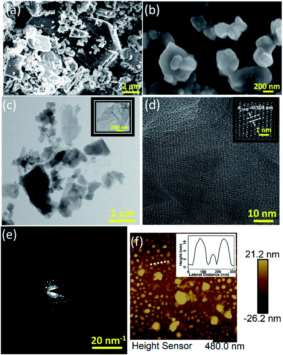 | ||
| Fig. 1 FESEM image of (a) bulk boron and (b) exfoliated boron nanostructures, (c) Large area low magnification TEM image of the as-exfoliated nanostructure (inset: magnified image of an individual nanoparticle) (d) its HR-TEM image (inset: atomic resolution image) (e) corresponding SAED pattern and (f) AFM image (inset: height profile) of the as-obtained nanomaterial. | ||
The continuous lattice fringe (as shown in Fig. 1(d)) clearly indicates the high crystallinity of the nanostructures, which is further confirmed by the SAED pattern in reciprocal space as shown in Fig. 1(e). A zoomed version of this HRTEM image gives us a lattice spacing of 0.504 nm which corresponds to the (104) plane of β-rhombohedral boron as also reported in the literature recently.30
The AFM results indicate that most of the sheets are 4–10 nm thick with their lateral dimension in the range of a few hundred nanometres to a few microns (thickness vs. lateral dimension plot of a nanostructure is shown in Fig. 1(f)) which is well suited for device fabrication. Seeing the irregular shapes and concave edges of boron nanostructures, we performed Raman measurements of a sample which was scanned by AFM to avoid any confusion with solvent marks. The corresponding Raman data (Fig. S4(b)†) of the sample whose AFM image is shown in Fig. S4(a)† clearly indicate that the nanostructures are truly elemental boron. After morphological confirmation of exfoliation, it was necessary to ascertain the extent of exfoliation. Fig. 2(a) shows the comparison of the X-ray diffraction patterns of bulk boron and exfoliated nanostructures. It is clearly seen that the XRD peaks in the exfoliated boron have shifted to lower two-theta values due to nanostructuring (2θ for bulk boron = 56.28°; 2θ value for the exfoliated boron nanostructure = 56.17°, with change in Δ2θ = 0.11° for (107)). However, the crystallinity of the boron nanostructure is maintained which corroborates the TEM results. We couldn't observe any sharp absorption peak in its UV/Vis absorption spectra (as shown in Fig. 2(b)); however, Raman spectroscopy has shown a few notable differences. A comparison of the Raman spectra of bulk boron and boron nanostructures is shown in Fig. 2(c). It is evident that a few suppressed peaks (like those at 531.32 cm−1) have evolved due to new lattice vibrations in boron nanostructures upon exfoliation. Apart from this, the ratio of X and Y peaks (X & Y peaks in boron nanostructures and corresponding peaks in bulk boron are denoted by X′ and Y′) of A1g + E1g Raman active modes and their ratio seem to be very crucial in explaining the extent of exfoliation. For instance, in this case, the intensity ratio of peaks X and Y (IX/IY) in nanostructured boron is found to be greater than one (IX/IY > 1) while the ratio of the same peak in bulk boron is less than one (IX′/IY′ < 1). This may be due to the difference in inter-icosahedral vibration levels in bulk and nanostructured boron. Also, the peak positions of the two peaks are found to be shifted after nanostructuring. A red shift of 1.91 cm−1 is observed in the X peak, while the Y peak shifts significantly (5.94 cm−1) in nanostructured boron compared to its bulk counterpart. However, more systematic studies on the Raman spectrum of boron are needed in the future.
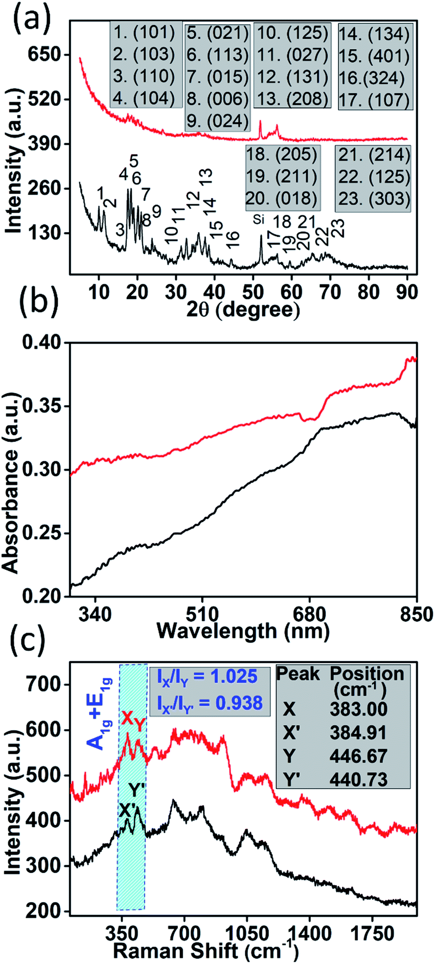 | ||
| Fig. 2 Comparative data for bulk boron (shown by the black line) and boron nanostructures (shown by the red line): (a) XRD, (b) UV/Vis and (c) Raman spectra (Ij, j = X, Y, X′, and Y′ represent the intensity of the corresponding peak, for instance IX = intensity of the X peak). | ||
The purity of the element was confirmed through high-angle annular dark-field imaging (HAADF)-scanning transmission electron microscope (STEM) elemental mapping as shown in Fig. 3. It is clearly evident that abundant oxygen is present in the sample along with the elemental boron. However, the sample hasn't been oxidised as observed by XRD and spectroscopic characterization. These oxygen molecules may play a crucial role in gas sensing similar to other good gas sensing materials like metal oxides, TMDs, carbon derivatives etc.
 | ||
| Fig. 3 (a) Large area HAADF image, (b) elemental mapping of boron nanostructures (as obtained via sonication), (c) elemental mapping of oxygen, and (d) imposition of elemental mapping on the HAADF image. | ||
The exfoliated boron nanostructure remained well dispersed even after 3 months. No deviation in XRD data of the exfoliated boron nanomaterial after such a long time (as shown in Fig. S9 (ESI†)) clearly indicates that it is stable in ambient atmosphere which further suggests that it is a good choice for receptor materials in chemical sensors.
The exfoliated boron nanostructures were further dropcast on a Ti/Pt (10 nm/90 nm) interdigitated electrode (IDE) of 5 μm gap and calcined at 100 °C for half-an-hour to obtain a two-terminal chemiresistive gas sensing device (more details in ESI Note S1 and optical micrographs in S6, ESI†).
The device was exposed to several oxidising and reducing gases in a custom-built gas sensing set-up (Fig. S1, ESI†), out of which it was found to be selectively responding to CH4 (Fig. S5, ESI†). The dynamic response (%) of the device was obtained by subjecting the device to variable methane concentrations from 105 ppm to 50 ppm and again back to 105 ppm which is shown in Fig. 4(a). It should be noted here that the response (R%) percentage of the device was calculated as
 | (1) |
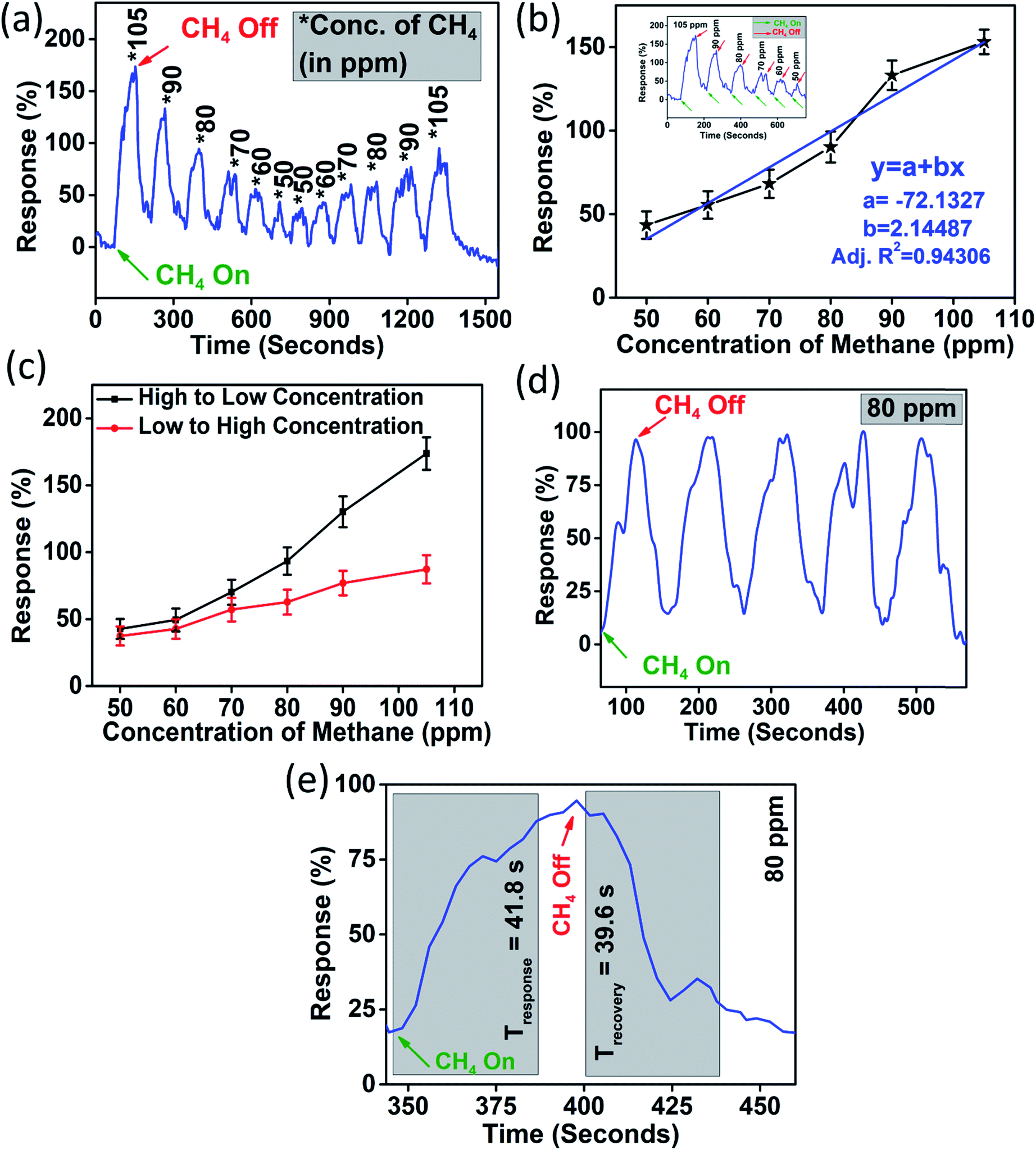 | ||
| Fig. 4 (a) Dynamic response of the device to methane gas when it is subjected to 105 ppm to 50 ppm and again 50 ppm to 105 ppm, (b) linearity of the device for one cycle of response (105 ppm to 50 ppm), (c) hysteresis of the device, (d) repeatability of the device when subjected to 80 ppm of methane gas for five consecutive cycles and (e) response and recovery time for 80 ppm of methane gas. | ||
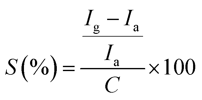
The first cycle of the device response was fitted to a linear equation (as shown in Fig. 4(b)) and it showed a coefficient of correlation greater than 0.9 (∼0.94). The sensitivity (S) of the device is calculated as
 | (2) |
We observe a sensitivity of 2.14% ppm−1 for the device in the methane concentration range of 50–105 ppm. Another important factor which limits sensor performance is the hysteresis associated with it. Hysteresis depth (Hmax) associated with the device can be calculated as
 | (3) |
Furthermore, it was necessary to ascertain the repeatability of the device. Fig. 4(d) shows the gas sensor response for five consecutive methane exposures (of 80 ppm). The device retained a similar rise and fall times for all five cycles in the repeatability test. The sensor was found to be quick enough to respond and recover. The response time and recovery time for 80 ppm methane gas were measured and they were found to be 41.8 seconds and 39.6 seconds, respectively, as shown in Fig. 4(e).
Methane is a non-polar symmetric molecule where a high enthalpy carbon–hydrogen bond gives it more stability in the gaseous phase which makes its dissociation and subsequently its detection tough.32
To understand the gas sensing behaviour, it was necessary to understand the chemical and textural properties at the surface of the exfoliated boron nanostructure and its bulk counterpart, which could be done by XPS analysis and nitrogen adsorption–desorption analysis, respectively. The surface states of the exfoliated and bulk boron don't vary chemically as interpreted from the XPS (XPS survey data are shown in Fig. S10†) signature in B 1s and O 1s spectra as shown in Fig. 5(a–d). The O 1s spectra in both the samples showed a large quantity of surface adsorbed oxygen species. The electron paramagnetic resonance (EPR) measurements in the literature33 showed that these surface adsorbed oxygen species easily obtain electrons from the surface of the nanomaterial as follows:
| O2(gas) → O2(ads) | (4) |
| O2(ads) + e− → O2(ads)− | (5) |
 | ||
| Fig. 5 (a) B 1s XPS spectrum of boron and (b) O 1s spectrum of bulk boron, (c) B 1s XPS spectrum and (d) O 1s spectrum of the exfoliated boron nanostructure; nitrogen adsorption–desorption characterization of (e) bulk boron and (f) exfoliated boron nanostructures. | ||
When the sensing device is exposed to methane gas, it reacts with the adsorbed oxygen ion species on the boron nanostructures as follows:
| CH4 + 2O2(ads)− → 2H2O + CO2 + 2e− | (6) |
The electrons released in this interaction further increase the conductivity of the boron nanostructures where electrons are the major current carrier. This ionosorption model is widely followed by the sensor community and is highly dependent on the density of oxygen species on the surface which in turn demands high specific area of the nanostructures used as the receptor film.34 According to the adsorption–desorption isotherms (Fig. 5(e and f)), the BET surface area of the exfoliated boron sample was determined to be 15.69 m2 g−1 which is almost 1.74 times that of the bulk boron sample (with BET surface area = 9.04 m2 g−1).
The ultrathin nature of the nanostructures ensures the high surface-to-volume ratio which ultimately results in good response. We compared the boron nanostructure based device with other high performance chemiresistive methane sensors as shown in Fig. 6 (with further details in Tables S1 and S2, ESI†) and found that this device is highly competitive, with better or comparable performance with existing technology in terms of experimental limits of detection, response and recovery time, sensitivity, and operating temperature.35–46
 | ||
| Fig. 6 Benchmarking (on log–log plot) of our work with the literature reports on methane gas sensors. Star (★) shows the data points and operating temperatures are represented with marks as shown in the figure. Data points are labelled with [Reference, Limit of Detection] which indicates the corresponding reference number and its LOD (in ppm). | ||
Conclusions
We synthesized boron nanostructures via ultrasonic irradiation in a low boiling point solvent medium. A chemiresistive device fabricated with this nanomaterial as the sensing film showed promising methane sensing. In particular, excellent linear response (43.5–153.1%) for a large range of methane concentrations (50 ppm to 105 ppm), repeatability, and good response and recovery time make this device attractive for the said application. The room temperature operation of the device makes it less power hungry. However, the high hysteresis depth and cross sensitivity associated with the device remain a challenge for the research community and should be addressed for the development of next generation methane sensors.Conflicts of interest
There are no conflicts to declare.Acknowledgements
The authors acknowledge funding support from MHRD, DeitY, DST Nano mission through NNetRA. NB would also like to thank the INAE and SERB for Abdul Kalam Technology Innovation National Fellowship. RJ would like to acknowledge SERB for the national postdoctoral fellowship. We acknowledge the technical support provided by staff members at National Nano Fabrication Facility (NNFC) and Micro and Nano Characterization Facility (MNCF) at the Centre for Nano Science and Engineering (CeNSE), Indian Institute of Science, Bangalore, India. We thank Ms Nithya Gorur from the National Institute of Engineering, Mysore for her support in materials preparation during her internship at the CeNSE. We also thank Dr R. J. Deshpande, Senior Scientific Officer, Materials Engineering Department, IISc, Bangalore.References
- K. L. Cashdollar, I. A. Zlochower, G. M. Green, R. A. Thomas and M. Hertzberg, J. Loss Prev. Process Ind., 2000, 13, 327–340 CrossRef.
- D. Kunkel, R. J. Basseri, M. D. Makhani, K. Chong, C. Chang and M. Pimentel, Dig. Dis. Sci., 2011, 56, 1612–1618 CrossRef CAS PubMed.
- T. Iseki, H. Tai and K. Kimura, Meas. Sci. Technol., 2000, 11, 594 CrossRef CAS.
- P. K. Sekhar, J. Kysar, E. L. Brosha and C. R. Kreller, Sens. Actuators, B, 2016, 228, 162–167 CrossRef CAS.
- C. Zheng, W. Ye, N. P. Sanchez, C. Li, L. Dong, Y. Wang, R. J. Griffin and F. K. Tittel, Sens. Actuators, B, 2017, 244, 365–372 CrossRef CAS.
- J. Yang, L. Zhou, X. Che, J. Huang, X. Li and W. Chen, Sens. Actuators, B, 2016, 235, 717–722 CrossRef CAS.
- G. Gong and H. Zhu, Luminescence, 2016, 31, 183–189 CrossRef CAS PubMed.
- Y. Xia, J. Wang, L. Xu, X. Li and S. Huang, Sens. Actuators, B, 2020, 304, 127334 CrossRef.
- T. Järvinen, G. S. Lorite, J. Peräntie, G. Toth, S. Saarakkala, V. K. Virtanen and K. Kordas, Nanotechnology, 2019, 30, 405501 CrossRef PubMed.
- M. G. Stanford, K. Yang, Y. Chyan, C. Kittrell and J. M. Tour, ACS Nano, 2019, 13, 3474–3482 CrossRef CAS PubMed.
- W. Yuan and G. Shi, J. Mater. Chem. A, 2013, 1, 10078–10091 RSC.
- R. K. Jha and N. Bhat, Adv. Mater. Interfaces, 2020, 1901992 CrossRef.
- H.-J. Koh, S. J. Kim, K. Maleski, S.-Y. Cho, Y.-J. Kim, C. W. Ahn, Y. Gogotsi and H.-T. Jung, ACS Sens., 2019, 4, 1365–1372 CrossRef CAS PubMed.
- E. Lee, A. VahidMohammadi, Y. S. Yoon, M. Beidaghi and D.-J. Kim, ACS Sens., 2019, 4, 1603–1611 CrossRef CAS PubMed.
- M. Sajjad and P. Feng, Mater. Res. Bull., 2014, 49, 35–38 CrossRef CAS.
- S. Cui, H. Pu, S. A. Wells, Z. Wen, S. Mao, J. Chang, M. C. Hersam and J. Chen, Nat. Commun., 2015, 6, 8632 CrossRef CAS PubMed.
- B. Kiraly, X. Liu, L. Wang, Z. Zhang, A. J. Mannix, B. L. Fisher, B. I. Yakobson, M. C. Hersam and N. P. Guisinger, ACS Nano, 2019, 13, 3816–3822 CrossRef CAS PubMed.
- S. M. Beladi-Mousavi, A. M. Pourrahimi, Z. Sofer and M. Pumera, Adv. Funct. Mater., 2019, 29, 1807004 Search PubMed.
- Y. Valadbeigi, H. Farrokhpour and M. Tabrizchi, J. Chem. Sci., 2015, 127, 2029–2038 CrossRef CAS.
- A. Shahbazi Kootenaei and G. Ansari, Phys. Lett. A, 2016, 380, 2664–2668 CrossRef CAS.
- Z. Rostami and H. Soleymanabadi, J. Mol. Model., 2016, 22, 70 CrossRef PubMed.
- A. Omidvar, Comput. Theor. Chem., 2017, 1115, 179–184 CrossRef CAS.
- V. Shukla, J. Wärnå, N. K. Jena, A. Grigoriev and R. Ahuja, J. Phys. Chem. C, 2017, 121, 26869–26876 CrossRef CAS.
- B. Peng, H. Zhang, H. Shao, Y. Xu, R. Zhang and H. Zhu, J. Mater. Chem. C, 2016, 4, 3592–3598 RSC.
- E. S. Penev, S. Bhowmick, A. Sadrzadeh and B. I. Yakobson, Nano Lett., 2012, 12, 2441–2445 CrossRef CAS PubMed.
- Z. Zhang, A. J. Mannix, Z. Hu, B. Kiraly, N. P. Guisinger, M. C. Hersam and B. I. Yakobson, Nano Lett., 2016, 16, 6622–6627 CrossRef CAS PubMed.
- B. Kiraly, X. Liu, L. Wang, Z. Zhang, A. J. Mannix, B. L. Fisher, B. I. Yakobson, M. C. Hersam and N. P. Guisinger, ACS Nano, 2019, 13, 3816–3822 CrossRef CAS PubMed.
- B. Feng, J. Zhang, Q. Zhong, W. Li, S. Li, H. Li, P. Cheng, S. Meng, L. Chen and K. Wu, Nat. Chem., 2016, 8, 563 CrossRef CAS PubMed.
- X. Liu, L. Wang, S. Li, M. S. Rahn, B. I. Yakobson and M. C. Hersam, Nat. Commun., 2019, 10, 1–7 CrossRef PubMed.
- H. Li, L. Jing, W. Liu, J. Lin, R. Y. Tay, S. H. Tsang and E. H. T. Teo, ACS Nano, 2018, 12, 1262–1272 CrossRef CAS PubMed.
- Y. Jiang, N. Tang, C. Zhou, Z. Han, H. Qu and X. Duan, Nanoscale, 2018, 10, 20578–20586 RSC.
- P. Hong, Y. Li, X. Zhang, S. Peng, R. Zhao, Y. Yang, Z. Wang, T. Zou and Y. Wang, J. Mater. Sci.: Mater. Electron., 2019, 30, 14325–14334 CrossRef CAS.
- M. Kooti, S. Keshtkar, M. Askarieh and A. Rashidi, Sens. Actuators, B, 2019, 281, 96–106 CrossRef CAS.
- A. Gurlo and R. Riedel, Angew. Chem., Int. Ed., 2007, 46, 3826–3848 CrossRef CAS PubMed.
- P. Bhattacharyya, P. K. Basu, B. Mondal and H. Saha, Microelectron. Reliab., 2008, 48, 1772–1779 CrossRef CAS.
- A. Biaggi-Labiosa, F. Sola, M. Lebrón-Colón, L. Evans, J. Xu, G. Hunter, G. Berger and J. Gonzalez, Nanotechnology, 2012, 23, 455501 CrossRef CAS PubMed.
- N. Shaalan, M. Rashad and M. Abdel-Rahim, Mater. Sci. Semicond. Process., 2016, 56, 260–264 CrossRef CAS.
- N. Shaalan, M. Rashad, A. Moharram and M. Abdel-Rahim, Mater. Sci. Semicond. Process., 2016, 46, 1–5 CrossRef CAS.
- J. Hu, F. Gao, Z. Zhao, S. Sang, P. Li, W. Zhang, X. Zhou and Y. Chen, Appl. Surf. Sci., 2016, 363, 181–188 CrossRef CAS.
- D. Zhang, H. Chang, C. Jiang, Y. Yao and Y. Zhang, Sens. Actuators, B, 2017, 252, 624–632 CrossRef CAS.
- D. Zhang, H. Chang, P. Li and R. Liu, J. Mater. Sci.: Mater. Electron., 2016, 27, 3723–3730 CrossRef CAS.
- K. C. Lam, B. Huang and S.-Q. Shi, J. Mater. Chem. A, 2017, 5, 11131–11142 RSC.
- J. Liang, J. Liu, N. Li and W. Li, J. Alloys Compd., 2016, 671, 283–290 CrossRef CAS.
- T. Sen, S. Mishra, S. Sonawane and N. G. Shimpi, Polym. Eng. Sci., 2018, 58, 1438–1445 CrossRef CAS.
- A. Mosahebfard, H. D. Jahromi and M. H. Sheikhi, IEEE Sens. J., 2016, 16, 4174–4179 Search PubMed.
- Z. P. Tshabalala, K. Shingange, B. Dhonge, O. Ntwaeaborwa, G. H. Mhlongo and D. E. Motaung, Sens. Actuators, B, 2017, 238, 402–419 CrossRef CAS.
Footnote |
| † Electronic supplementary information (ESI) available. See DOI: 10.1039/c9na00749k |
| This journal is © The Royal Society of Chemistry 2020 |