
 Open Access Article
 This Open Access Article is licensed under a
 Creative Commons Attribution 3.0 Unported Licence
Phosphorus doped SnO2 thin films for transparent conducting oxide applications: synthesis, optoelectronic properties and computational models†
Michael J.
Powell
 a,
Benjamin A. D.
Williamson
ab,
Song-Yi
Baek
a,
Joe
Manzi
a,
Dominic B.
Potter
a,
David O.
Scanlon
abc and
Claire J.
Carmalt
*a
a,
Benjamin A. D.
Williamson
ab,
Song-Yi
Baek
a,
Joe
Manzi
a,
Dominic B.
Potter
a,
David O.
Scanlon
abc and
Claire J.
Carmalt
*a
aDepartment of Chemistry, University College London, 20 Gordon Street, London WC1H 0AJ, UK. E-mail: c.j.carmalt@ucl.ac.uk
bThomas Young Centre, University College London, Gower Street, London WC1E 6BT, UK
cDiamond Light Source Ltd, Diamond House, Harwell Science and Innovation Campus, Didcot, Oxfordshire OX11 0DE, UK
First published on 23rd August 2018
Abstract
Phosphorus doped tin(IV) oxide (P:SnO2) films have been synthesised by an aerosol assisted chemical vapour deposition route. Triethyl phosphate was used as the phosphorus dopant source. The phosphorus concentration in solution was found to be key to electrical properties, with concentrations between 0.25–0.5 mol% phosphorus giving the lowest resistivities of the deposited films. The conductivity of the films synthesised improved on doping SnO2 with phosphorus, with resistivity values of 7.27 × 10⁻⁴ Ω cm and sheet resistance values of 18.2 Ω □−1 achieved for the most conductive films. Phosphorus doping up to 1.0 mol% was shown to improve visible light transmission of the deposited films. The phosphorus doping also had a significant effect on film morphology, with varying microstructures achieved. The films were characterised by X-ray diffraction, scanning electron microscopy, UV/vis spectroscopy, Hall effect measurements and X-ray photoelectron spectroscopy. The data generated was used to build computational models of phosphorus as a dopant for SnO2, showing that the phosphorus acts as a shallow one-electron n-type donor allowing for good conductivities. Phosphorus does not suffer from self-compensation issues associated with other dopants, such as fluorine.
1. Introduction
Transparent conducting oxides (TCOs) are fundamentally important in solar cells,1–3 flat-screen displays,4,5 organic light emitting diodes,6,7 touchscreen displays8,9 and liquid crystal displays.10 There are several techniques for depositing thin films of TCO materials, including, magnetron sputtering,11–13 spray pyrolysis,14,15 atmospheric pressure chemical vapour deposition,16,17 aerosol assisted chemical vapour deposition (AACVD)18,19 and sol–gel synthesis.20,21For industrial production of TCO materials high throughput techniques, such as chemical vapour deposition and magnetron sputtering, are favoured for producing conformal coatings over large areas of substrate. Atmospheric pressure CVD can deliver high growth rates, with highly conformal coatings and are used commercially in the production of functional coatings, such as Pilkington Activ™. Doping of materials by atmospheric pressure CVD techniques is not a trivial matter. This is due to the incorporation of the dopant being controlled by the vapour pressure of the precursor, small changes in temperature or gas flow rate can lead to dramatic changes in incorporation of dopants into the host matrix.
Aerosol assisted CVD relies on the ability to produce an aerosol from a solution containing a suitable metal precursor. This eliminates the need for the precursor to be volatile, with the precursor only needing to be soluble in a suitable solvent, i.e. a solvent that can be atomised to generate a mist, for synthesis to be achieved.22 This allows for a far larger range of precursors to be used for the synthesis of functional thin film coatings. In a typical AACVD reaction, the aerosol is carried to the reaction chamber by a carrier gas, where it passes over a heated substrate resulting in nucleation, reaction and film growth. AACVD has several advantages for depositing materials, such as greater sustainability,23 a wider range of precursors, precise control over dopant concentrations and ease of co-doping materials.22 AACVD also has the potential to be a scalable process, although consideration of the choice of solvent would be critical, with water being the ideal solvent for sustainability, safety and reduction of unwanted waste products.24
Wide-bandgap (above 3.1 eV) semiconductor metal oxides, such as indium tin oxide (ITO),25–27 Al-doped zinc oxide (AZO)28–30 and F-doped tin oxide (FTO)5,31,32 are commonly employed for use as TCOs. ITO has been shown to have film resistivities as low as 5 × 10⁻⁵ Ω cm, mobilities of ca. 100 cm2 V−1 s−1 and charge carrier densities of 1.5 × 1021 cm−3.33 For AZO, film resistivities of 2 × 10⁻⁴ Ω cm, mobilities of ca. 50 cm2 V−1 s−1 and charge carrier densities of 5 × 1020 cm−3 have been reported.34 FTO has been shown to have film resistivities as low as 4 × 10⁻⁴ Ω cm, mobilities of ca. 40 cm2 V−1 s−1 and charge carrier densities of 4 × 1020 cm−3.5 ITO is the most commonly used TCO material in industry, owing to the low resistivity, high charge carrier concentration and high charge carrier mobility of the material.35 ITO, however, is expensive due to the high price of extracting and processing indium.36 There are also concerns over the relative scarcity of indium and the competing demands for indium from flat-screen displays and photovoltaic applications.37 As a consequence, there has been a focus on producing TCO materials that do not require the use of indium.
Tin(IV) oxide is an ideal candidate for use as a TCO material. Undoped SnO2 has a band-gap of ∼3.6 eV making it transparent to visible wavelengths,38 it is also intrinsically an n-type semiconductor and can be doped to improve its electrical properties. Common dopants to improve the electrical properties include; fluorine,5,31,39 antimony,40–42 tantalum43–46 and niobium.46–48 Although there have been limited reports on the use of phosphorus as a dopant to improve electrical properties,49–53 to the best of our knowledge, there has yet to be a report on the use of phosphorus doping of tin(IV) oxide synthesised by AACVD. Outlined in this paper is the effect that the phosphorus precursor, triethyl phosphate, has on the electrical, visible and morphological properties of SnO2 thin films deposited by AACVD. Coupled to the experimental work are computational studies that explore why phosphorus is an effective n-type dopant for SnO2 and showing how the phosphorus contributes to the improvement of the functional properties of the deposited films. Combining the experimental and computational results displays the potential of further increasing the functional properties of SnO2 thin films for TCO materials.
2. Experimental
All chemicals were used as bought, without further purification: monobutyltin trichloride (95%, Sigma-Aldrich), triethyl phosphate (99.8%, Sigma-Aldrich) and methanol (99.9%, Fisher), were used as the tin and phosphorus precursors and solvent respectively. Compressed air (21% (±0.5%) O2 in N2) was used as the carrier gas for all reactions, supplied from BOC. The glass substrate used for depositions was 3.2 mm thick plain float glass with a 50 nm thick SiO2 barrier layer (Pilkington/NSG).2.1 Thin film synthesis
In a typical deposition, triethyl phosphate (0.0136 g, 7.5 mmol) was added to BuSnCl3 (0.3 g, 1.1 mmol) dissolved in methanol (20 mL) with stirring. The methanol solution was allowed to stir for ca. 10 min. Varying molar ratios of the P to Sn precursor were used to deposit a range of films. In the 7.5 mol% P:Sn film, the amount of triethyl phosphate to use (0.0136 g, 7.5 mmol) was calculated from the amount of BuSnCl3 in the solution. Precursor solutions containing 0.0, 0.1, 0.25, 0.5, 1, 1.5, 5 and 7.5 mol% P:Sn content were prepared in this manner.The AACVD thin film depositions were carried out as detailed elsewhere.31 Briefly, a carbon block heater comprising the lower half of the reactor was used to maintain the substrate temperature using a k-type thermocouple. Depositions were carried out on Pilkington silica-coated barrier glass (50 nm SiO2 coated on one side of float glass) in order to prevent unwanted leaching of ions from the glass into the thin film.54 Prior to deposition, the glass substrates were cleaned with soapy water, isopropanol and acetone and were then left to air dry. The substrate was then loaded into the reaction chamber along with a second piece of float glass suspended 8 mm above (silica barrier layer pointing down) to ensure laminar flow during deposition. An aerosol mist of the precursor solution was generated using a ‘Liquifog’ piezo ultrasonic atomizer from Johnson Matthey, which uses an operating frequency of 1.6 MHz to produce a mode droplet size of ca. 3 μm. The mist was transported into the reactor via a baffle, using compressed air, as the carrier gas, at a constant flow-rate of 1.0 L min−1. The exhaust of the reactor was vented into a fume cupboard. When the precursor solution and associated aerosol mist had been completely emptied from the bubbler, the coated substrate was cooled to below 100 °C before being removed from the reactor. Deposition temperatures were fixed at 550 °C, as below this temperature carbon contamination made the films less visibly transparent. Typical deposition times were between 30–40 min. Sample descriptions can be found in Table 1.
![[thin space (1/6-em)]](https://www.rsc.org/images/entities/char_2009.gif) :Sn ratio from EDX. All samples were deposited at 550 °C with compressed air used as the carrier gas. The mol% of triethyl phosphate in precursor solution is given and the at% P in the resulting film as determined from EDX. Undoped lattice parameters and cell volume values were obtained from ICSD reference SnO2 (9163-ICSD)
:Sn ratio from EDX. All samples were deposited at 550 °C with compressed air used as the carrier gas. The mol% of triethyl phosphate in precursor solution is given and the at% P in the resulting film as determined from EDX. Undoped lattice parameters and cell volume values were obtained from ICSD reference SnO2 (9163-ICSD)
| Sample description mol% of triethyl phosphate in solution | Lattice parameter a = b (Å) | Lattice parameter c (Å) | Cell volume (Å3) | P:Sn ratio in film/at% |
|---|---|---|---|---|
| Undoped SnO2 thin film | 4.738(1) | 3.187(2) | 71.53 | — |
| 0.1% P:SnO2 thin film | 4.749(1) | 3.181(1) | 71.75(2) | — |
| 0.25% P:SnO2 thin film | 4.7444(5) | 3.1905(6) | 71.82(1) | — |
| 0.5% P:SnO2 thin film | 4.7449(4) | 3.1880(7) | 71.78(2) | 0.26:99.74 |
| 1.0% P:SnO2 thin film | 4.7419(1) | 3.190(1) | 71.70(3) | 0.62:99.38 |
| 1.5% P:SnO2 thin film | 4.737(1) | 3.188(1) | 71.53(3) | 0.69:99.31 |
| 5.0% P:SnO2 thin film | 4.740(2) | 3.184(2) | 71.55(4) | 1.42:98.58 |
| 7.5% P:SnO2 thin film | 4.745(2) | 3.182(2) | 71.65(5) | — |
2.2 Thin film characterisation
Scanning electron microscope images were recorded on a Jeol JSM-6301F SEM at an acceleration voltage of 5 kV. X-ray diffraction (XRD) patterns were recorded using a Bruker D8 Discover X-ray diffractometer using monochromatic Cu Kα1 and Cu Kα2 radiation of wavelengths 1.54056 and 1.54439 Å respectively, emitted in an intensity ratio of 2:1 with a voltage of 40 kV and a current of 40 mA. The incident beam angle was 1° and data was collected between 5° and 66° 2θ with a step size of 0.05° at 1.0 s per step. All diffraction patterns obtained were compared with database standards (ICSD). Unit cell volumes and lattice parameters were calculated from the XRD data using GSAS and EXPGUI programs. X-ray photoelectron spectroscopy was conducted on a Thermo Scientific K-alpha spectrometer with monochromated Al Kα radiation, a dual beam charge compensation system and constant pass energy of 50 eV (spot size 400 μm). Survey scans were collected in the binding energy range 0–1200 eV. High-resolution peaks were used for the principal peaks of Sn (3d), O (1s), P (2s) and C (1s). Data was calibrated against C 1s (285.0 eV). Data was fitted using CASA XPS software. UV/vis spectra were recorded on a Perkin Elmer Lambda 950 UV/vis/NIR Spectrophotometer in both transmission and diffuse reflectance mode. A Labsphere reflectance standard was used as a reference for the UV/vis measurements. Room temperature Hall effect measurements were carried out on an Ecopia HMS-3000 set up in the Van der Pauw configuration. Measurements were taken using a 0.58 T permanent magnet and a current of 1 μA. Tests were carried out on square-cut samples measuring ≈1 × 1 cm. Silver paint (Agar Scientific) was used to form ohmic contacts, which were tested on the in-built software prior to measurement. The Hall effect method was used to find the ρ, μ and n using measured film thickness values as obtained from a Filmetrics F20 machine operating in reflectance mode in air against an as-supplied SnO2 standard.
2.3 Computational modelling
 | (1) |
| μSn + 2μO = ΔHSnOf2 = −5.27 eV (experiment = 5.98 eV (ref. 77)) | (2) |
Two growth conditions; Sn-rich/O-poor (n-type favourable) and Sn-poor/O-rich (p-type favourable) regimes can therefore be defined limited by the growth of Sn(s) and O2(g) respectively:
| Sn-rich/O-poor conditions: μSn = 0 eV; μO = −2.64 eV | (3) |
| Sn-poor/O-rich conditions: μSn = −5.27 eV; μO = 0 eV | (4) |
The solubilities of the phosphorus species are limited by the formation of a secondary phase, P2O5:
| 2μP + 5μO = ΔHPf2O5 = −14.80 eV (experiment = −15.59 eV (ref. 78)) | (5) |
The thermodynamic transition levels (q/q′) can be calculated using the equation:
 | (6) |
And show the evolution of a defect from charge state q to q′ at a certain Fermi level position. These are useful experimentally as they can be seen in techniques such as deep level transient spectroscopy (DLTS).
Dependence on oxygen partial pressure and temperature. In order to gain a snapshot of the defect chemistry under experimental conditions, the dependence of μO on the oxygen partial pressure and temperature can be determined using the equation:79
 | (7) |
 .80,81 The P:SnO2 films were carried out using AACVD at ∼900 K/1 atm allowing us to determine the oxygen chemical potential using data from thermochemical tables,82 therefore: μO(T,p0) = −0.97 eV.
3. Results and discussion
3.1 Thin film characterisation
Thin films of P-doped SnO2 (P:SnO2) were synthesised from monobutyltin trichloride and triethyl phosphate by aerosol assisted chemical vapour deposition (AACVD) with compressed air as the carrier gas. The concentration of the phosphorus was varied in solution. All films were synthesised at 550 °C, with typical deposition times being 30–40 min.The films were analysed for their elemental content via energy-dispersive X-ray spectroscopy (EDX) and X-ray photoelectron spectroscopy (XPS). XPS was also used to determine the oxidation state and environments for the elements present in the synthesised film, as shown in Fig. 1. In the XPS, the Sn 3d and P 2s environments were probed, since the Sn 3d and P 2p regions overlap and hence the P 2s had to be used to determine the oxidation state of the phosphorus. For all films deposited, there was only a single Sn environment, which gave values of 487.0 and 495.2 eV for the Sn 3d5/2 and Sn 3d3/2 respectively. These values matched with literature values for SnO2 (±0.2 eV).83,84 The oxygen environment gave a combination of O–Sn and O–C at 530.6 and 532.4 eV respectively (±0.2 eV), in agreement with literature values.85,86 The P 2s peak occurred at a value of 191.2 eV (±0.2 eV), which is commonly seen for phosphorus in the 5+ state.87,88 As the phosphorus precursor, triethyl phosphate, also formally has the phosphorus as P5+, this suggests that the phosphorus was not reduced when it was incorporated into the SnO2 lattice. This is not surprising, as the depositions were performed in an oxygen rich environment, which should keep the phosphorus in its maximum oxidation state.
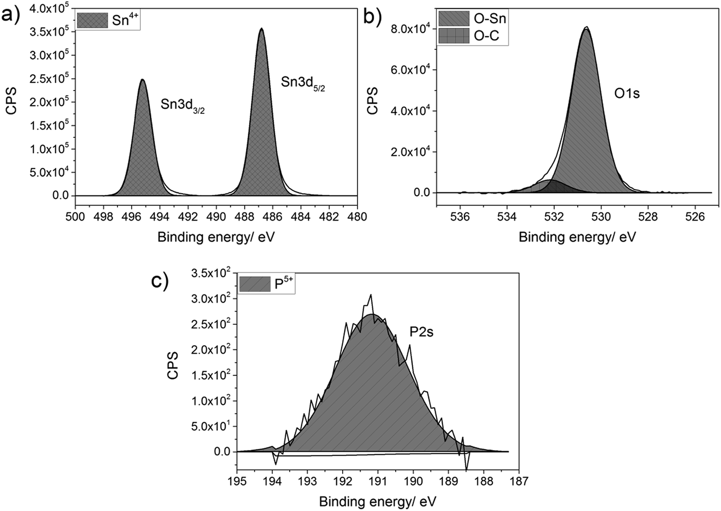 | ||
| Fig. 1 Typical X-ray photoelectron spectra for (a) Sn 3d environment, (b) O 1s environment and (c) P 2s environment for P-doped SnO2 films synthesised by AACVD at 550 °C. | ||
Although phosphorus was detected within the XPS data, the signal was weak with a high noise to signal ratio, which indicates that the at% of phosphorus in all the P-doped samples were ∼1 at% or below, since this is the threshold of reliable detection for XPS. Therefore, although the phosphorus can be detected and can be seen in both the change in morphology from the SEM images and change in electrical resistivity from the Hall effect data (vide infra), the measured values cannot be included as the error on these would be larger than the value calculated from the XPS data.
To determine whether the phosphorus was segregated in the films, or uniformly dispersed, depth profiling was performed on the samples. This showed that the phosphorus was bulk segregated, with the P to Sn ratio increasing on etching of the films. In order to determine the amount of P present in each of the films EDX was used. The EDX results showed a gradual increase in the P content in the films with increasing mol% P precursor in the AACVD precursor solution (Table 1) from 0.5 mol% until 5 mol%. For films deposited using ≤0.25 mol% and 7.5 mol% triethyl phosphate, the P content in the films was too low to be accurately reported (<0.1 at%) although XPS and the observed change in morphology and XRD (vide infra) provide evidence of low quantities of P in these films. AACVD precursor solutions containing 0.5, 1.0 and 1.5 mol% triethyl phosphate produced SnO2 films with 0.26, 0.62 and 0.69 at% P, respectively. The films formed from 5 mol% triethyl phosphate in the precursor solution contained 1.42 at% before doping to very low levels using 7.5 mol%, suggesting possible saturation was reached at 5 mol% P. A similar effect was observed in the deposition of Sb-doped TiO2 films via AACVD where precursor solutions with >2.5 mol% Sb inhibited the incorporation of Sb in the TiO2 and reduction of the Sb(OEt)3 precursor occurred.89
X-ray diffraction (XRD) was used to determine the phase present in the samples synthesised, Fig. 2. All XRD patterns displayed diffraction peaks that were referenced to the cassiterite phase of SnO2. The incorporation of phosphorus has several effects on the patterns displayed. The most obvious change was to the intensity of the (110) plane, this was the most intense diffraction peak for the undoped SnO2 film. On incorporation of phosphorus, however, the intensity of the reflection of this plane was significantly reduced in the XRD data. The intensity of this diffraction peak then remains low throughout the various phosphorus dopant concentrations. This suggests that phosphorus retards crystal growth in this direction.
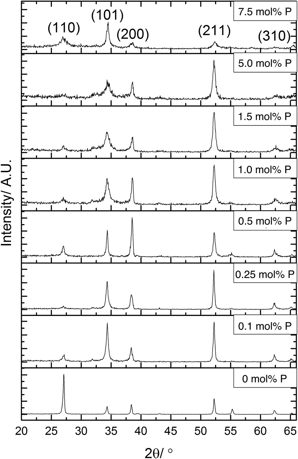 | ||
| Fig. 2 X-ray diffraction patterns for P:SnO2 thin films deposited by AACVD at 550 °C. A change in preferred orientation is observed between undoped, and inclusion of phosphorus into the crystal structure. | ||
Preferred orientation was observed in (101) and (211) planes for films formed using ≤0.25 mol% triethyl phosphate. The (200) plane was suppressed when using 1.5 mol% or higher P precursor, with preferred orientation occurring in the (101)/(200)/(211) planes for films formed with 0.5 mol% and 1.0 mol% triethyl phosphate. The highest amount of 7.5 mol% P precursor showed that the (211) plane was also suppressed. Preferred orientation in the (211) plane has been observed previously for Sb-doped SnO2 films.90,91 For F-doped SnO2 thin films, a preferential orientation towards the (200) is commonly observed for highly conductive films.5,92
It was noticeable that at high dopant concentrations, the phosphorus appeared to reduce the overall crystallinity of the films since all the diffraction peaks become weaker and less well defined. Interestingly, this effect was only displayed for the (211) plane at concentrations above 5 mol% triethyl phosphate in the precursor solution, whereas the (101) and (200) display this reduction in intensity at lower concentrations of phosphorus. This has been previously observed for phosphorus doped SnO2 films synthesised by the simultaneous oxidation of phosphine and tetramethyltin,49 where above 3.2 at% phosphorus content, the crystallinity of the films rapidly diminished.
From the XRD patterns a shifting of the diffraction peaks to higher angles at greater phosphorus concentrations was observed. This suggests that phosphorus was being incorporated into the SnO2 lattice, with the smaller ionic radius of P(V) (34 pm compared to Sn(IV) which is 71 pm) leading to a reduction in the lattice parameters.
The data from the XRD patterns was used to calculate the lattice parameters for the films and observe how these were affected by the inclusion of phosphorus, as shown in Table 1. Due to the poor crystallinity of the films at higher dopant concentrations, there was a higher error in the calculated unit cell volumes. The trend apparent in the data showed that phosphorus incorporation leads to a reduction of the crystal lattice. Although there is an apparent initial increase in lattice parameters, this is within the error for the data quality and so is most likely an artefact of the model used to calculate the lattice parameter data. As the phosphorus in the precursor is in the 5+ state, it will most likely replace on tin sites. With phosphorus being a smaller atom than tin, this would lead to a reduction in lattice parameters, which is seen for higher doping levels.
To determine the effect of phosphorus doping on the morphology of the deposited SnO2 films, scanning electron microscopy (SEM) images were obtained for all samples, Fig. 3. As with the XRD patterns, Fig. 2, the incorporation of phosphorus had a large effect, such that a variation in surface morphology of the deposited samples was observed. Undoped SnO2, Fig. 3a, displayed typical pyramidal structures associated with SnO2 deposited by AACVD processes.93
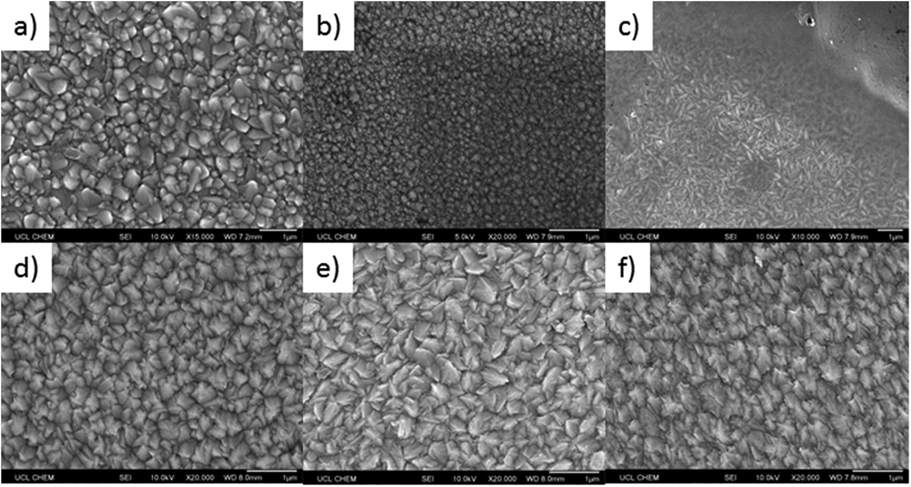 | ||
| Fig. 3 Typical SEM images showing the surface morphology for (a) undoped SnO2, (b) 0.1 mol% P:SnO2, (c) 0.25 mol% P:SnO2, (d) 0.5 mol% P:SnO2, (e) 1.0 mol% P:SO2, and (f) 1.5 mol% P:SnO2 thin films on glass. All samples were produced at 550 °C, by aerosol assisted CVD using compressed air as the carrier gas. | ||
Phosphorus doping has a remarkable effect on the morphology of the samples. Even at low %mol in solution (0.1 mol%), Fig. 3b, a lowering of the average size of the particles present was observed. The particles are also much rounder, with a loss of the pyramidal shape. With higher phosphorus %mol in the precursor solution, the particles become more rod-like in shape. This is supported in the XRD patterns for this sample (0.25 mol%), where the (101) plane had high intensity and the (110) plane was very low in intensity, this is known to favour rod-like particle formation for SnO2.94 Interestingly, although films formed using 0.1 mol% and 0.25 mol% P precursor in solution show similar XRD patterns and relative preferred orientations, the 0.1 mol% has a higher relative intensity in the (110) plane, which appears to prevent the growth of the rod-like particles.
The other feature in the morphology for films deposited using 0.25 mol% triethyl phosphate in solution (Fig. 3c) is the presence of a continuous layer that covers the rod-like particles; this is shown in the top right hand corner of the image. This uniform layer does not appear to be made of any obvious individual particles, which suggests that phosphorus incorporation can control grain boundary growth. Control of grain boundaries has been shown to improve the properties of graphene,95 silicon96 and zirconia97 layers/thin films.
With increasing phosphorus %mol in the starting precursor solution, the pyramidal particle shape was once again present. The particle shapes were not, however, identical to undoped SnO2. The particles were more angular and jagged, resembling shark's teeth, Fig. 3d–f. This coincides with a loss in intensity in the (101) plane for the XRD patterns for these samples and a change in preferential orientation to the (200) plane for films deposited using 0.5 mol% P precursor. This type of morphology has been previously observed for F-doped SnO2 with preferred orientation in the (200) plane.98
UV/vis spectra were obtained for all deposited films to determine the effect of the incorporation of phosphorus on the optical properties of the films, Fig. 4. As shown, the phosphorus incorporation initially led to a small increase in the visible light transmission of the films formed using 0.25 mol% triethyl phosphate in the precursor solution which gave visible light transmission ca. 82% (400–700 nm), this was above the visible light transmission of the undoped sample (80.8%). Further increasing the concentration, however, led to a significant worsening of the visible light transmission. Films that were deposited from solutions with higher than 1 mol% triethyl phosphate had a significant yellow hue to their colour, when observed in transmission, so it is not surprising that these films were poorer at allowing visible light to be transmitted. Colour centres are known to be caused by defects, such as oxygen vacancies, with doping of metal oxides often leading to an increase in the number of these defects.99,100
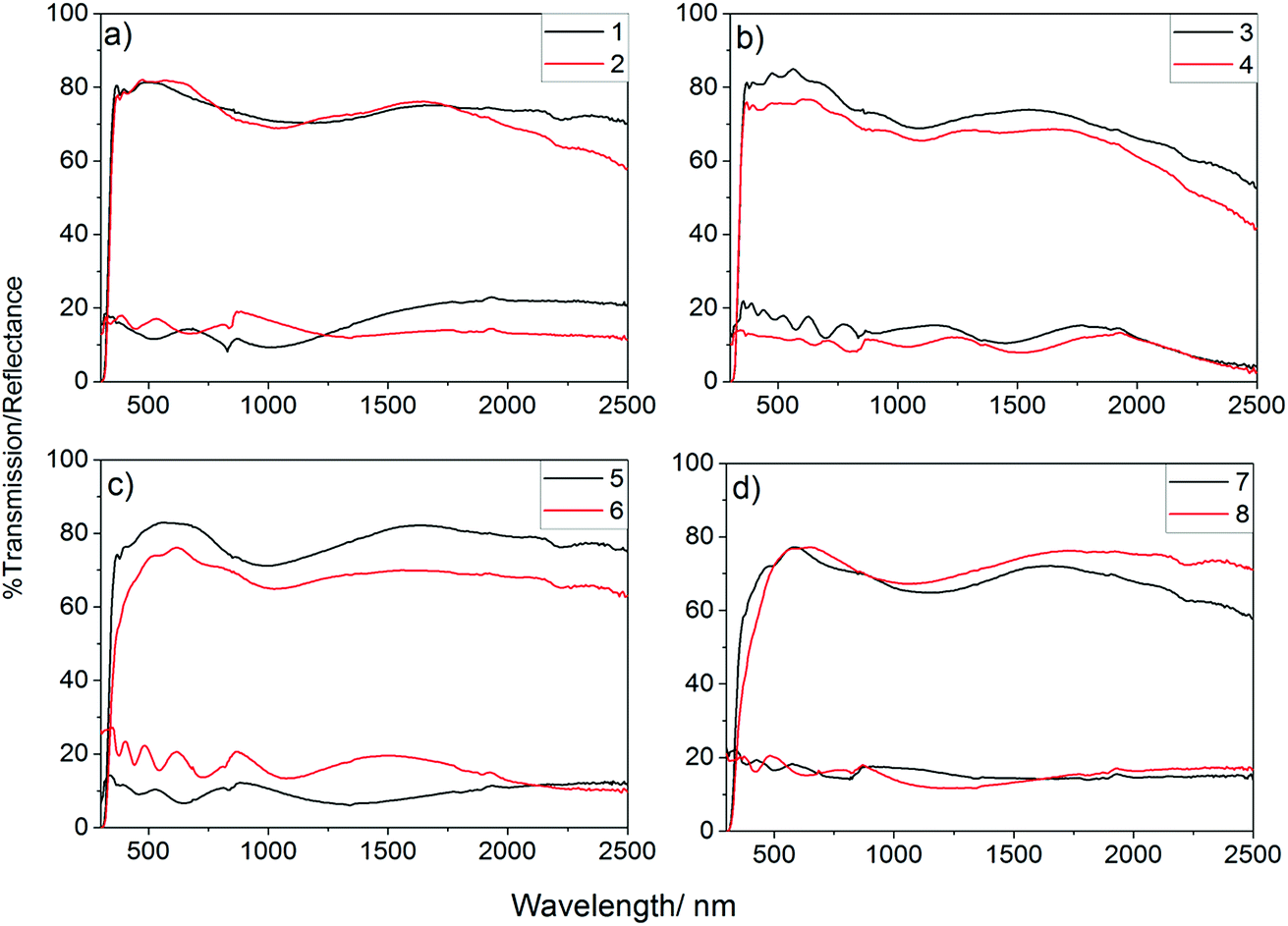 | ||
| Fig. 4 UV/vis/NIR spectra for P-doped SnO2 films; (a) undoped SnO2 (1) and 0.1 mol% P:SnO2 (2); (b) 0.25 mol% P:SnO2 (3) and 0.5 mol% P:SnO2 (4); (c) 1 mol% P:SnO2 (5) and 1.5 mol% P:SnO2 (6); and (d) 5 mol% P:SnO2 (7) and 7.5 mol% P:SnO2 (8). In all cases the films showed high transmission (ca. 80%) and low reflection (<20%). All films deposited by AACVD at 550 °C using air as carrier gas. | ||
3.2 Functional testing
In order to determine the electrical properties of the deposited films, Hall effect measurements were obtained, shown in Table 2. Undoped SnO2 and the use of high concentrations of triethy phosphate (7.5 mol% P) led to films that were too resistive for the Hall effect to measure the electrical properties. Increasing the amount of phosphorus doping (0.26–1.42 at% P in the films from 0.5–5 mol% triethyl phosphate precursor), however, had a dramatic impact on the resistivity values, as shown in Fig. 5. There was a clear trend observed in the data, where by increasing the phosphorus level from 0.1 to 0.5 mol% in solution led to films with improved electrical properties. The reduction in resistivity was accompanied by an increase in carrier density and mobility. At higher phosphorus doping, the electrical properties deteriorated, such that a slight increase in resistivity and reductions in charge carrier densities and mobilities were observed (films formed from 1.0 and 1.5 mol% triethyl phosphorus). Interestingly, the values recovered again around 5 mol% phosphorus in solution, before again becoming highly resistive above 7 mol%. The lowest resistivity values were for the films that were formed using 0.5 mol% triethyl phosphorus resulting in 0.26 at% P in the films. These films had resistivity values of 7.27 × 10⁻⁴ Ω cm, sheet resistance of 18.2 Ω □−1 and charge carrier mobility of 35.2 μ cm−2 V1 s1, these values are comparable to industry standards for F-doped SnO2 thin films, as shown in Table 2.| Sample | d μm−1 | n/×1020 cm−3 | μ/cm2 V−1 s−1 | ρ/×10−3 Ω cm | R Sh/Ω □−1 | T λ550/% | T λ400–700/% |
|---|---|---|---|---|---|---|---|
| a d: film thickness (±0.02 μm); n: charge carrier concentration; μ: charge carrier mobility; ρ: bulk resistivity; Rsh: sheet resistance; Tλ550; transmittance at 550 nm; Tλ400–700: average transmittance over visible light range, 400–700 nm. | |||||||
| Undoped SnO2 | 0.40 | N/A | N/A | N/A | N/A | 80.9 | 80.8 |
| 0.1 mol% | 0.40 | 0.80 | 22.5 | 3.48 | 87.1 | 81.6 | 82.2 |
| 0.25 mol% | 0.40 | 2.23 | 27.6 | 1.00 | 25.0 | 84.5 | 83.8 |
| 0.5 mol% | 0.40 | 2.44 | 35.2 | 0.73 | 18.2 | 76.7 | 79.3 |
| 1.0 mol% | 0.40 | 1.70 | 34.1 | 1.08 | 27.0 | 82.8 | 82.4 |
| 1.5 mol% | 0.40 | 2.73 | 17.8 | 1.31 | 32.7 | 74.0 | 73.4 |
| 5.0 mol% | 0.40 | 2.76 | 23.6 | 0.96 | 24.0 | 76.0 | 74.4 |
| 7.5 mol% | 0.40 | N/A | N/A | N/A | N/A | 76.1 | 72.6 |
|
|||||||
| Commercial standards | |||||||
| TEC™8 | 0.65 | 5.3 | 28 | 0.52 | 8.0 | 83 | 82 |
| TEC™15 | 0.35 | 5.6 | 21 | 0.53 | 15.1 | 85 | 83 |
| Asahi U™ | 0.90 | 2.2 | 32 | 0.88 | 9.8 | ||
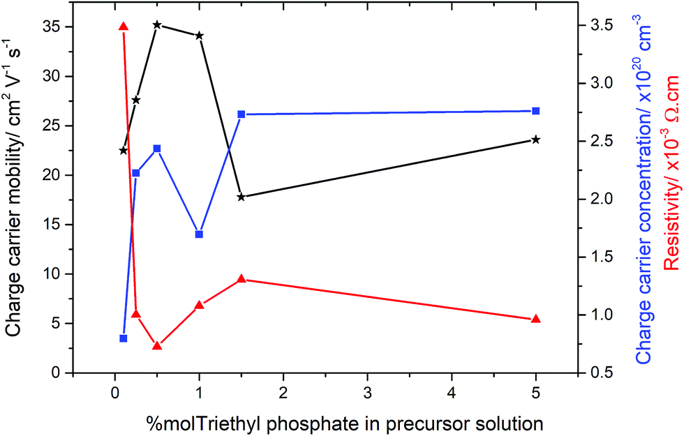 | ||
| Fig. 5 Electrical properties for the P-doped SnO2 films as obtained by Hall effect measurements. | ||
Interestingly, the most conductive film (from 0.5 mol% triethyl phosphate) displayed preferential orientation in the (200) plane, which is commonly seen for highly conductive SnO2 films.101,102 However, the other films formed from 0.25, 1.0, 1.5 and 5 mol% P precursor, display preferred orientation in the (211) plane but were still highly conductive. This suggests that the origin of the increased electrical conductivity is not the product of a particular crystallographic orientation, but a mix of morphological and electronic contributions.
The most surprising value about the doping of these films is the low level of phosphorus required to achieve improvements in electrical properties. Even using only 0.1 mol% P precursor resulted in a significant increase in the electrical conductivity of the deposited films. Conversely increasing phosphorus concentrations above 1.5 mol%, the electrical properties deteriorated. This was accompanied by the films becoming highly coloured, with a yellow hue obvious in the deposited films. This suggests that the phosphorus forms colour centres when in higher concentrations, with these colour centres also acting as places where either recombination or deflection of the electrons can occur.103 Although F-doping of SnO2 also requires low levels of incorporation, between 0.5–1 at%, phosphorus doping by AACVD requires even smaller levels of incorporation into the lattice.
Using the Hall effect data it was also possible to establish the dominant scattering mechanism for the films. This was achieved by plotting the mobility values against the charge carrier concentrations. For all the samples synthesised for this study, the mobilities were relatively low (17–35 cm2 V−1 s−1), whilst the charge carrier concentrations were relatively high (0.8–2.7 × 1020 cm−3), this suggests that the dominant scattering mechanism for all samples is due to grain boundary scattering. This type of scattering mechanism is typical of polycrystalline SnO2 thin films.104
These results show that phosphorus is an effective dopant for the synthesis of highly conductive n-type TCO thin films. Phosphorus doping also has a large impact on the preferred orientation and morphology of the films deposited, with low levels of phosphorus leading to round and rod-like particles with the development of pyramidal structures being observed at higher levels of doping, ca. 0.5 mol% triethyl phosphate in the precursor solution. Rod-like structures of SnO2 have been used for gas sensing applications,105,106 so being able to select for this kind of morphology by incorporation of a dopant is of potential interest.
Furthermore, phosphorus doping of SnO2 opens up a new direction for the development of TCO materials synthesised by aerosol assisted CVD. Although the electrical properties of these films were not as high as for the best quoted values for F-doped SnO2, they are still comparable to industry standards. The phosphorus dopant, triethyl phosphate has low toxicity, whereas many of the fluorine precursors are highly toxic. This makes the handling, storage and disposal of the phosphorus precursor easier, cheaper and safer than for common fluorine precursors, such as ammonium fluoride.
3.3 Computational modelling and results
The experimental work described above indicates that phosphorus is an effective n-type dopant for SnO2 and functional properties required for TCOs can be achieved. In order to explore how the phosphorus contributes to the improvement of the functional properties of the deposited films computational models of phosphorus as a dopant for SnO2 have been carried out. Phosphorus could potentially act both as an acceptor and donor dopant substituting on both O and Sn sites, as well as incorporating interstitially. Hence, theoretical calculations have been carried out on each of these defect environments as well as for the dominant intrinsic donor (VO) and acceptor (VSn) defects.The transition level diagrams under Sn-rich/O-poor, 900 K, 1 atm and Sn-poor/O-rich conditions are shown in Fig. 6.
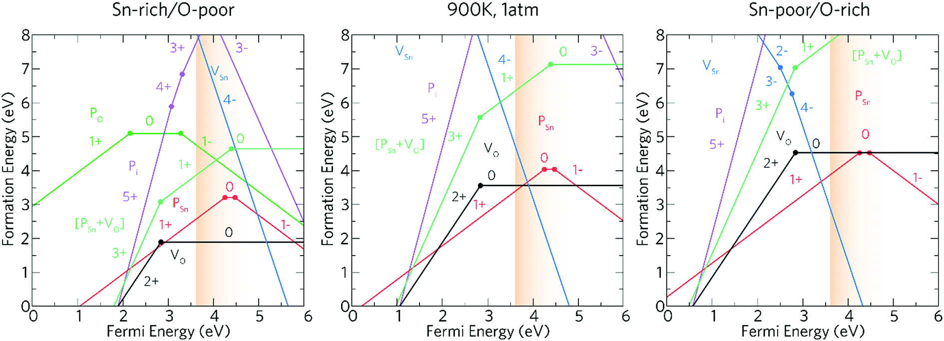 | ||
| Fig. 6 The charge transition level diagrams for Sn-rich/O-poor (left), 900 K, 1 atm (middle) and Sn-poor/O-rich (right). The Fermi energy goes from the VBM (0 eV) to ∼2.4 eV above the CBM (which is at 3.6 eV). The conduction band region is depicted by the graded orange area. | ||
Oxygen vacancies, VO, and tin vacancies, VSn, act as the two lowest energy intrinsic donor and acceptor defects respectively in SnO2. VO is a negative-U defect and a deep donor with the 2+/0 transition level occurring ∼0.76 eV below the conduction band minimum (CBM) and as such, does not contribute significantly to the conductivity. This behaviour is in keeping with other theoretical69,107,108 and experimental109,110 results. VO is a negative-U defect in other TCOs, such as ZnO,69,111–113 In2O3 (ref. 69 and 114–116) and BaSnO3 (ref. 67) and has been identified via positron annihilation spectroscopy.117 The neutral charge state of VSn occurs very high in energy under all growth regimes (under favourable Sn-poor/O-rich conditions, the formation energy is ∼8.37 eV) acting as a deep acceptor with the 0/1− transition level occurring ∼1.75 eV above the VBM.
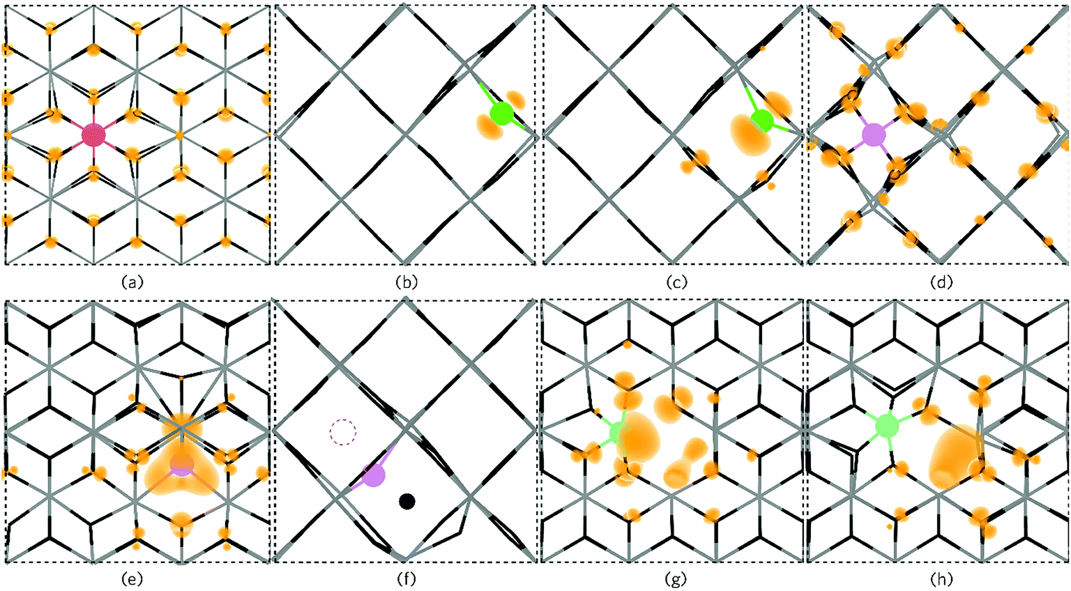 | ||
| Fig. 7 The partial electron charge densities (orange) for (a) PSn viewed along {010} with a charge density of 0.002 eV A−1, (b) P0O and (c) PO1− as viewed along the {001} direction with a charge density of 0.02 eV A−1. Pi3+ is depicted in (d) along the {001} direction with a charge density of 0.008 eV A−1 and Pi3− is shown in (e) along {010} with a charge density of 0.02 eV A−1 where a large triple polaron is seen. In (f), Pi3− is viewed along the {001} axis presenting the displacement of a lattice O to an interstitial site by P (the original interstitial position is shown by the dashed circle). (g) and (h) displays the defect cluster [PSn + VO] in both the neutral and 1+ charge states respectively as viewed along {010} and plotted from 0–0.01 eV A−1. In each panel the SnO2 is depicted by the grey (Sn) and black (O) wire frame model with the P species colour coded to Fig. 6. | ||
| EBE = E[SbSn+VO] + Ehost − ESbSn − EVO |
Under Sn-rich/O-poor, 900 K, 1 atm and Sn-poor/O-rich growth conditions, the neutral charge state of [PSn + VO] is 4.64 eV, 7.13 eV and 8.59 eV respectively.121,122 It is likely, therefore, that this defect complex will form in negligible quantities or possibly form at high doping concentrations. [PSn + VO] acts as a shallow one-electron donor in SnO2 with the 1+/0 transition level occurring around 0.74 eV above the CBM. A further transition level (3+/1+) occurs in the band gap at 0.82 eV below the CBM. Fig. 7g and h show the partial charge electron density for [PSn + VO] in both the neutral (Fig. 7g) and 1+ (Fig. 7h) charge states. In the neutral charge state, the electron density can be seen to localise on the P and in the oxygen vacancy. In the 1+ charge state, an electron has been removed from the P atom leaving two electrons in the oxygen vacancy. It is therefore reasonable to assume that phosphorus remains in the 5+ oxidation state and that the formation of this defect complex exists due to lattice strain.
Based on the above results, our calculations show that P:SnO2 is a shallow one-electron n-type donor allowing for good conductivities. Phosphorus does not suffer from self-compensation issues like F:SnO2,123 however, towards higher doping concentrations the incorporation of P may need a non-equilibrium deposition technique due to the increase in formation energy. The computational calculations agree with the experimental observations, such that phosphorus was incorporated as P5+ (from XPS), and the conductivity of the films synthesised improved on doping SnO2 with phosphorus, with resistivity values of 7.27 × 10⁻⁴ Ω cm and sheet resistance values of 18.2 Ω □−1 achieved for the most conductive films, as expected for a one-electron n-type dopant. Moreover, only low dopant levels of P in the SnO2 were achieved, which correlate with the theoretical results indicating that incorporation of P under equilibrium conditions could be difficult. Combining the experimental results with computational modelling allowed for the determination of the effectiveness of phosphorus as a dopant for SnO2.
4. Conclusions
P-doped SnO2 thin films with excellent optical and electrical properties were synthesised by aerosol assisted chemical vapour deposition. The best performing films had a sheet resistance of 18.2 Ω □−1, charge carrier mobility of 35.2 μ cm−2 V1 s1 and resistivity of 7.27 × 10⁻⁴ Ω cm−1 which is comparable to industry standards. The phosphorus was shown to have a significant impact on the preferential orientation, morphology and crystallinity of the films, with a range of different morphologies observed in the microstructure of the polycrystalline films. Combining the experimental results with computational modelling allowed the determination of the effectiveness of phosphorus as a dopant for SnO2. Phosphorus has been shown to be a shallow level n-type dopant with the electrons possessing excellent mobility. This synthetic route opens up the possibility of using a common element to dope SnO2 films for transparent conducting oxide applications.Author contributions
S. B., M. J. P., D. B. P. and J. M. contributed experimental and characterisation techniques, B. A. D. W. contributed the computational modelling, D. O. S. and C. J. C. supervised the work, all authors contributed to writing the manuscript.Conflicts of interest
The authors declare no conflict of interest.Acknowledgements
The authors would like to thank the EPSRC for grants EP/L017709 and EP/N01572X/1 and UCL for an impact studentship (D. B. P.). This work made use of the ARCHER UK National Supercomputing Service (http://www.archer.ac.uk) via our membership of the UK's HEC Materials Chemistry Consortium, which is also funded by the EPSRC (EP/L000202). The UCL Legion and Grace HPC Facilities (Legion@UCL and Grace@UCL) were also used in the completion of this work. Dr Sanjayan Sathivasam is thanked for the EDX measurements. Pilkington Glass NSG limited is thanked for supplying glass substrates.References
- Y. Ooyama, Y. Shimada, Y. Kagawa, I. Imae and Y. Harima, Org. Biomol. Chem., 2007, 5, 2046–2054 RSC.
- M. R. Leyden, L. K. Ono, S. R. Raga, Y. Kato, S. Wang and Y. Qi, J. Mater. Chem. A, 2014, 2, 18742–18745 RSC.
- D. J. Lewis and P. O'Brien, Chem. Commun., 2014, 50, 6319–6321 RSC.
- P. Marchand, I. A. Hassan, I. P. Parkin and C. J. Carmalt, Dalton Trans., 2013, 42, 9406–9422 RSC.
- N. Noor and I. P. Parkin, J. Mater. Chem. C, 2013, 1, 984–996 RSC.
- S. H. K. Park, M. Ryu, C. S. Hwang, S. Yang, C. Byun, J. I. Lee, J. Shin, S. M. Yoon, H. Y. Chu and K. I. Cho, Electrochem. Solid-State Lett., 2008, 11, H10–H14 CrossRef.
- B. Geffroy, P. Le Roy and C. Prat, Polym. Int., 2006, 55, 572–582 CrossRef.
- D. R. Cairns, D. C. Paine and G. P. Crawford, Appl. Phys. Lett., 2001, 78, 2643–2645 CrossRef.
- S. W. Heo, Y. D. Ko, Y. S. Kim and D. K. Moon, J. Mater. Chem. C, 2013, 1, 7009–7019 RSC.
- M. Bremer, P. Kirsch, M. Klasen-Memmer and K. Tarumi, Angew. Chem., Int. Ed., 2013, 52, 8880–8896 CrossRef PubMed.
- S. Lee, S.-H. Kim, Y. Kim, A. I. Kingon, D. C. Paine and K. No, Mater. Lett., 2012, 85, 88–90 CrossRef.
- R. Pandey, C. H. Wie, X. Lin, J. W. Lim, K. K. Kim, D. K. Hwang and W. K. Choi, Sol. Energy Mater. Sol. Cells, 2015, 134, 5–14 CrossRef.
- K.-J. Ahn, J.-H. Park, B.-K. Shin, W. Lee, G. Y. Yeom and J.-M. Myoung, Appl. Surf. Sci., 2013, 271, 216–222 CrossRef.
- H. Faber, B. Butz, C. Dieker, E. Spiecker and M. Halik, Adv. Funct. Mater., 2013, 23, 2828–2834 CrossRef.
- N. Rashidi, V. L. Kuznetsov, J. R. Dilworth, M. Pepper, P. J. Dobson and P. P. Edwards, J. Mater. Chem. C, 2013, 1, 6960–6969 RSC.
- A. Kafizas, N. Noor, P. Carmichael, D. O. Scanlon, C. J. Carmalt and I. P. Parkin, Adv. Funct. Mater., 2014, 24, 1758–1771 CrossRef.
- C. Sotelo-Vazquez, N. Noor, A. Kafizas, R. Quesada-Cabrera, D. O. Scanlon, A. Taylor, J. R. Durrant and I. P. Parkin, Chem. Mater., 2015, 27, 3234–3242 CrossRef.
- D. B. Potter, D. S. Bhachu, M. J. Powell, J. A. Darr, I. P. Parkin and C. J. Carmalt, Phys. Status Solidi A, 2016, 213, 1346–1352 CrossRef.
- C. E. Knapp, G. Hyett, I. P. Parkin and C. J. Carmalt, Chem. Mater., 2011, 23, 1719–1726 CrossRef.
- S. Salam, M. Islam and A. Akram, Thin Solid Films, 2013, 529, 242–247 CrossRef.
- M. M. Koebel, D. Y. Nadargi, G. Jimenez-Cadena and Y. E. Romanyuk, ACS Appl. Mater. Interfaces, 2012, 4, 2464–2473 CrossRef PubMed.
- C. E. Knapp and C. J. Carmalt, Chem. Soc. Rev., 2016, 45, 1036–1064 RSC.
- M. J. Powell and C. J. Carmalt, Chem.–Eur. J., 2017, 23, 15543–15552 CrossRef PubMed.
- M. J. Powell, D. B. Potter, R. L. Wilson, J. A. Darr, I. P. Parkin and C. J. Carmalt, Mater. Des., 2017, 129, 116–124 CrossRef.
- D. Angmo, S. A. Gevorgyan, T. T. Larsen-Olsen, R. R. Søndergaard, M. Hösel, M. Jørgensen, R. Gupta, G. U. Kulkarni and F. C. Krebs, Org. Electron., 2013, 14, 984–994 CrossRef.
- L. Barraud, Z. Holman, N. Badel, P. Reiss, A. Descoeudres, C. Battaglia, S. De Wolf and C. Ballif, Sol. Energy Mater. Sol. Cells, 2013, 115, 151–156 CrossRef.
- H. Kim, C. Gilmore, A. Pique, J. Horwitz, H. Mattoussi, H. Murata, Z. Kafafi and D. Chrisey, J. Appl. Phys., 1999, 86, 6451–6461 CrossRef.
- K. H. Kim, K. C. Park and D. Y. Ma, J. Appl. Phys., 1997, 81, 7764–7772 CrossRef.
- D. S. Bhachu, G. Sankar and I. P. Parkin, Chem. Mater., 2012, 24, 4704–4710 CrossRef.
- Y. Wu, S. Potts, P. Hermkens, H. Knoops, F. Roozeboom and W. Kessels, Chem. Mater., 2013, 25, 4619–4622 CrossRef.
- D. S. Bhachu, M. R. Waugh, K. Zeissler, W. R. Branford and I. P. Parkin, Chem.–Eur. J., 2011, 17, 11613–11621 CrossRef PubMed.
- T. Fukano and T. Motohiro, Sol. Energy Mater. Sol. Cells, 2004, 82, 567–575 Search PubMed.
- R. Bel Hadj Tahar, T. Ban, Y. Ohya and Y. Takahashi, J. Appl. Phys., 1998, 83, 2631–2645 CrossRef.
- T. Minami, H. Nanto and S. Takata, Jpn. J. Appl. Phys., 1984, 23, L280 CrossRef.
- K. Ellmer, Nat. Photonics, 2012, 6, 809–817 CrossRef.
- T. Minami, Thin Solid Films, 2008, 516, 5822–5828 CrossRef.
- C. Candelise, M. Winskel and R. Gross, Prog. Photovoltaics Res. Appl., 2012, 20, 816–831 CrossRef.
- Ç. Kılıç and A. Zunger, Phys. Rev. Lett., 2002, 88, 095501 CrossRef PubMed.
- M. Adnane, H. Cachet, G. Folcher and S. Hamzaoui, Thin Solid Films, 2005, 492, 240–247 CrossRef.
- B. Benrabah, A. Bouaza, A. Kadari and M. Maaref, Superlattices Microstruct., 2011, 50, 591–600 CrossRef.
- Y. Sun, W. D. Chemelewski, S. P. Berglund, C. Li, H. He, G. Shi and C. B. Mullins, ACS Appl. Mater. Interfaces, 2014, 6, 5494–5499 CrossRef PubMed.
- K. Peters, P. Zeller, G. Stefanic, V. Skoromets, H. Němec, P. Kužel and D. Fattakhova-Rohlfing, Chem. Mater., 2015, 27, 1090–1099 CrossRef.
- M. A. Gillispie, M. F. van Hest, M. S. Dabney, J. D. Perkins and D. S. Ginley, J. Mater. Res., 2007, 22, 2832–2837 CrossRef.
- S. woo Lee, Y.-W. Kim and H. Chena, Appl. Phys. Lett., 2001, 78, 350–351 CrossRef.
- A. Simões, A. Ries, E. Souza, L. Perazolli, M. Cilense, E. Longo and J. A. Varela, Ceram. Int., 2005, 31, 399–404 CrossRef.
- Y. Wang, T. Brezesinski, M. Antonietti and B. Smarsly, ACS Nano, 2009, 3, 1373–1378 CrossRef PubMed.
- M. Stefik, M. Cornuz, N. Mathews, T. Hisatomi, S. Mhaisalkar and M. Grätzel, Nano Lett., 2012, 12, 5431–5435 CrossRef PubMed.
- V. Gokulakrishnan, S. Parthiban, K. Jeganathan and K. Ramamurthi, J. Mater. Sci., 2011, 46, 5553–5558 CrossRef.
- Y. S. Hsu and S. K. Ghandhi, J. Electrochem. Soc., 1980, 127, 1592–1595 CrossRef.
- K. H. Yoon and D. J. Nam, J. Mater. Sci., 1995, 30, 3415–3420 CrossRef.
- L. Kőrösi, S. Papp, V. Meynen, P. Cool, E. F. Vansant and I. Dékány, Colloids Surf., A, 2005, 268, 147–154 CrossRef.
- J. Upadhyay, S. Vishwakarma and H. Prasad, Thin Solid Films, 1989, 169, 195–204 CrossRef.
- S. Vishwakarma and H. Prasad, J. Phys. D: Appl. Phys., 1993, 26, 959 CrossRef.
- A. Kafizas, C. Crick and I. P. Parkin, J. Photochem. Photobiol., A, 2010, 216, 156–166 CrossRef.
- G. Kresse and J. Furthmüller, Phys. Rev. B, 1996, 54, 11169 CrossRef.
- G. Kresse and J. Furthmüller, Comput. Mater. Sci., 1996, 6, 15–50 CrossRef.
- G. Kresse and J. Hafner, Phys. Rev. B: Condens. Matter Mater. Phys., 1993, 47, 558 CrossRef.
- G. Kresse and J. Hafner, Phys. Rev. B: Condens. Matter Mater. Phys., 1994, 49, 14251 CrossRef.
- P. E. Blöchl, Phys. Rev. B: Condens. Matter Mater. Phys., 1994, 50, 17953 CrossRef.
- C. Adamo and V. Barone, J. Chem. Phys., 1999, 110, 6158–6170 CrossRef.
- J. Paier, R. Hirschl, M. Marsman and G. Kresse, J. Chem. Phys., 2005, 122, 234102 CrossRef PubMed.
- D. O. Scanlon and G. W. Watson, J. Mater. Chem., 2012, 22, 25236–25245 RSC.
- A. M. Ganose and D. O. Scanlon, J. Mater. Chem. C, 2016, 4, 1467–1475 RSC.
- S. V. Farahani, T. D. Veal, J. J. Mudd, D. O. Scanlon, G. Watson, O. Bierwagen, M. White, J. S. Speck and C. F. McConville, Phys. Rev. B: Condens. Matter Mater. Phys., 2014, 90, 155413 CrossRef.
- Z. Lebens-Higgins, D. Scanlon, H. Paik, S. Sallis, Y. Nie, M. Uchida, N. Quackenbush, M. Wahila, G. Sterbinsky and D. A. Arena, Phys. Rev. Lett., 2016, 116, 027602 CrossRef PubMed.
- S. Sallis, D. Scanlon, S. Chae, N. Quackenbush, D. Fischer, J. Woicik, J.-H. Guo, S. Cheong and L. Piper, Appl. Phys. Lett., 2013, 103, 042105 CrossRef.
- D. O. Scanlon, Phys. Rev. B: Condens. Matter Mater. Phys., 2013, 87, 161201 CrossRef.
- J. Suffner, P. Ágoston, J. Kling and H. Hahn, J. Nanoparticle Res., 2010, 12, 2579–2588 CrossRef.
- P. Ágoston, K. Albe, R. M. Nieminen and M. J. Puska, Phys. Rev. Lett., 2009, 103, 245501 CrossRef PubMed.
- J. P. Allen, D. O. Scanlon, L. F. Piper and G. W. Watson, J. Mater. Chem. C, 2013, 1, 8194–8208 RSC.
- N. Quackenbush, J. Allen, D. Scanlon, S. Sallis, J. Hewlett, A. Nandur, B. Chen, K. Smith, C. Weiland and D. Fischer, Chem. Mater., 2013, 25, 3114–3123 CrossRef.
- R. M. Nieminen, Model. Simulat. Mater. Sci. Eng., 2009, 17, 084001 CrossRef.
- N. Hine, K. Frensch, W. Foulkes and M. Finnis, Phys. Rev. B: Condens. Matter Mater. Phys., 2009, 79, 024112 CrossRef.
- S. T. Murphy and N. D. Hine, Phys. Rev. B: Condens. Matter Mater. Phys., 2013, 87, 094111 CrossRef.
- S. Lany and A. Zunger, Phys. Rev. B: Condens. Matter Mater. Phys., 2008, 78, 235104 CrossRef.
- C. Freysoldt, J. Neugebauer and C. G. Van de Walle, Phys. Rev. Lett., 2009, 102, 016402 CrossRef PubMed.
- D. R. Lide, CRC Handbook of Chemistry and Physics, CRC Press, 86th edn, 2005 Search PubMed.
- M. W. Chase, NIST-JANAF Thermochemical Tables 2 Volume-Set (Journal of Physical and Chemical Reference Data Monographs), American Institute of Physics, 1998 Search PubMed.
- K. Reuter and M. Scheffler, Phys. Rev. B: Condens. Matter Mater. Phys., 2001, 65, 035406 CrossRef.
- F. H. Taylor, J. Buckeridge and C. R. A. Catlow, Chem. Mater., 2016, 28, 8210–8220 CrossRef.
- B. J. Morgan and G. W. Watson, J. Phys. Chem. C, 2010, 114, 2321–2328 CrossRef.
- D. R. Stull and H. Prophet, JANAF thermochemical tables, DTIC Document, 1971 Search PubMed.
- W.-K. Choi, J.-S. Cho, S.-K. Song, H.-J. Jung and S.-K. Koh, Jpn. J. Appl. Phys., 1996, 35, 5820 CrossRef.
- F. Vicent, E. Morallo, C. Quijada, J. Va, A. Aldaz and F. Cases, J. Appl. Electrochem., 1998, 28, 607–612 CrossRef.
- M. Kwoka, L. Ottaviano, M. Passacantando, S. Santucci, G. Czempik and J. Szuber, Thin Solid Films, 2005, 490, 36–42 CrossRef.
- P. Boulanger, J. Pireaux, J. Verbist and J. Delhalle, Polymer, 1994, 35, 5185–5193 CrossRef.
- T. Lindblad, B. Rebenstorf, Z.-G. Yan and S. L. T. Andersson, Appl. Catal., A, 1994, 112, 187–208 CrossRef.
- A. Osaka, Y. Miura and T. Tsugaru, J. Non-Cryst. Solids, 1990, 125, 87–92 CrossRef.
- D. S. Bhachu, R. G. Egdell, G. Sankar, C. J. Carmalt and I. P. Parkin, J. Phys. Chem. C, 2017, 5, 9694–9701 Search PubMed.
- D. Belanger, J. Dodelet, B. Lombos and J. Dickson, J. Electrochem. Soc., 1985, 132, 1398–1405 CrossRef.
- S.-Y. Lee and B.-O. Park, Thin Solid Films, 2006, 510, 154–158 CrossRef.
- A. Moholkar, S. Pawar, K. Rajpure, C. Bhosale and J. Kim, Appl. Surf. Sci., 2009, 255, 9358–9364 CrossRef.
- N. Noor and I. P. Parkin, Thin Solid Films, 2013, 532, 26–30 CrossRef.
- D. F. Zhang, L. D. Sun, J. L. Yin and C. H. Yan, Adv. Mater., 2003, 15, 1022–1025 CrossRef.
- Q. Yu, L. A. Jauregui, W. Wu, R. Colby, J. Tian, Z. Su, H. Cao, Z. Liu, D. Pandey and D. Wei, Nat. Mater., 2011, 10, 443–449 CrossRef PubMed.
- K. Kutsukake, N. Usami, Y. Ohno, Y. Tokumoto and I. Yonenaga, Appl. Phys. Express, 2013, 6, 025505 CrossRef.
- B. Alexandreanu, B. Capell and G. S. Was, Mater. Sci. Eng., 2001, 300, 94–104 CrossRef.
- E. Elangovan and K. Ramamurthi, Thin Solid Films, 2005, 476, 231–236 CrossRef.
- C. Fitzgerald, M. Venkatesan, L. S. Dorneles, R. Gunning, P. Stamenov, J. M. D. Coey, P. Stampe, R. Kennedy, E. C. Moreira and U. S. Sias, Phys. Rev. B: Condens. Matter Mater. Phys., 2006, 74, 115307 CrossRef.
- G. Liu, L. Wang, H. G. Yang, H.-M. Cheng and G. Q. M. Lu, J. Mater. Chem., 2010, 20, 831–843 RSC.
- S. Nakao, N. Yamada, T. Hitosugi, Y. Hirose, T. Shimada and T. Hasegawa, Appl. Phys. Express, 2010, 3, 031102 CrossRef.
- E. Elangovan and K. Ramamurthi, Appl. Surf. Sci., 2005, 249, 183–196 CrossRef.
- D. Lang and L. Kimerling, Phys. Rev. Lett., 1974, 33, 489 CrossRef.
- M. Prins, K.-O. Grosse-Holz, J. Cillessen and L. Feiner, J. Appl. Phys., 1998, 83, 888–893 CrossRef.
- Y. J. Chen, X. Y. Xue, Y. G. Wang and T. H. Wang, Appl. Phys. Lett., 2005, 87, 233503–233505 CrossRef.
- G. Xi and J. Ye, Inorg. Chem., 2010, 49, 2302–2309 CrossRef PubMed.
- P. Ágoston, C. Körber, A. Klein, M. J. Puska, R. M. Nieminen and K. Albe, J. Appl. Phys., 2010, 108, 053511 CrossRef.
- A. K. Singh, A. Janotti, M. Scheffler and C. G. Van de Walle, Phys. Rev. Lett., 2008, 101, 055502 CrossRef PubMed.
- S. Samson and C. Fonstad, J. Appl. Phys., 1973, 44, 4618–4621 CrossRef.
- P. King, R. Lichti, Y. Celebi, J. Gil, R. Vilão, H. Alberto, J. P. Duarte, D. Payne, R. Egdell and I. McKenzie, Phys. Rev. B: Condens. Matter Mater. Phys., 2009, 80, 081201 CrossRef.
- F. Oba, M. Choi, A. Togo and I. Tanaka, Sci. Technol. Adv. Mater., 2011, 12, 034302 CrossRef PubMed.
- F. Oba, S. R. Nishitani, S. Isotani, H. Adachi and I. Tanaka, J. Appl. Phys., 2001, 90, 824–828 CrossRef.
- A. Janotti and C. G. Van de Walle, Phys. Rev. B: Condens. Matter Mater. Phys., 2007, 76, 165202 CrossRef.
- A. Walsh, C. R. A. Catlow, A. A. Sokol and S. M. Woodley, Chem. Mater., 2009, 21, 4962–4969 CrossRef.
- S. Lany and A. Zunger, Phys. Rev. B: Condens. Matter Mater. Phys., 2009, 80, 085202 CrossRef.
- A. Goyal, P. Gorai, H. Peng, S. Lany and V. Stevanović, Comput. Mater. Sci., 2017, 130, 1–9 CrossRef.
- I. Makkonen, E. Korhonen, V. Prozheeva and F. Tuomisto, J. Phys.: Condens. Matter, 2016, 28, 224002 CrossRef PubMed.
- R. T. Shannon, Acta Crystallogr., Sect. A: Cryst. Phys., Diffr., Theor. Gen. Crystallogr., 1976, 32, 751–767 CrossRef.
- J. Varley, A. Janotti and C. Van de Walle, Phys. Rev. B: Condens. Matter Mater. Phys., 2010, 81, 245216 CrossRef.
- H. Peng, J. D. Perkins and S. Lany, Chem. Mater., 2014, 26, 4876–4881 CrossRef.
- J. Rockenberger, U. Zum Felde, M. Tischer, L. Tröger, M. Haase and H. Weller, J. Chem. Phys., 2000, 112, 4296–4304 CrossRef.
- V. Geraldo, V. Briois, L. V. D. A. Scalvi and C. Santilli, J. Eur. Ceram. Soc., 2007, 27, 4265–4268 CrossRef.
- J. E. Swallow, B. A. Williamson, T. J. Whittles, M. Birkett, T. J. Featherstone, N. Peng, A. Abbott, M. Farnworth, K. J. Cheetham and P. Warren, Adv. Funct. Mater., 2017, 28, 1701900 CrossRef.
- S. D. Ponja, B. O. Williamson, S. Sathasivam, D. O. Scanlon, I. P. Parkin and C. J. Carmalt, J. Mater. Chem. C, 2018, 6, 7257–7266 RSC.
Footnote |
| † Electronic supplementary information (ESI) available. See DOI: 10.1039/c8sc02152j |
| This journal is © The Royal Society of Chemistry 2018 |