
Side-chain engineering of perylenediimide-vinylene polymer acceptors for high-performance all-polymer solar cells†
Yikun
Guo
a,
Yunke
Li
b,
Omar
Awartani
c,
Han
Han
a,
Guangye
Zhang
b,
Harald
Ade
*c,
He
Yan
*b and
Dahui
Zhao
 *a
*a
aBeijing National Laboratory for Molecular Sciences, Chemistry, Centre for the Soft Matter Science and Engineering and the Key Laboratory of Polymer Chemistry and Physics of the Ministry of Education, College of Chemistry, Peking University, Beijing 100871, China. E-mail: dhzhao@pku.edu.cn
bDepartment of Chemistry and Hong Kong Branch of Chinese National Engineering Research Center for Tissue Restoration & Reconstruction, Hong Kong University of Science and Technology, Clear Water Bay, Kowloon, Hong Kong, China. E-mail: hyan@ust.hk
cDepartment of Physics, North Carolina State University, Raleigh, NC 27695, USA. E-mail: hwade@ncsu.edu
First published on 16th February 2017
Abstract
The side-chain structures of conjugated molecules are well recognized to sensitively influence the crystallinity, morphology and thus carrier transport properties of organic semiconductors. Here, by varying the alkyl side-chain length in the polymer acceptors, the effect of side-chain engineering on the photovoltaic performance is systematically studied in all-polymer solar cells. Clear trends of first an increase and then a decrease in the Jsc and FF values are observed as the branched alkyl groups are extended from 4 to 8 carbons. Correspondingly, the maximum average PCE (ca. 7.40%) is attained with an acceptor bearing a branched side-chain length of seven carbon atoms.
Introduction
The performance of all-polymer solar cells (all-PSCs) using n-type semiconducting polymers as the electron acceptor has witnessed significant improvements in the past few years.1 Compared to the fullerene derivatives, while offering comparable electron-transporting properties, polymeric acceptors boast many advantages, such as stronger light-absorption capability with tunable spectra, adjustable frontier orbital levels, solution-processing aptness, and higher active-layer morphological stability. All these features contribute to the great promise of further optimizing the device efficiency and the viable prospect of large-area fabrication.2–6 Recent studies have also shown that all-PSCs possess dramatically improved mechanical properties compared with fullerene-based PSCs, which makes them more suitable for flexible-device developments.7 Despite this promising potential, the best power conversion efficiency (PCE) reported to date for all-PSCs still lags behind the state-of-the-art values of fullerene-based PSCs.8–13 Only a few groups have realized all-PSCs with PCEs of over 7%.14–17 Therefore, developing high-performance polymeric acceptors and achieving higher PCEs are undoubtedly the most warranted tasks in the field of all-PSCs.Numerous studies with organic semiconductors have demonstrated that side-chain engineering can bring about prominent differences in a material’s properties and performance in devices, such as thin film transistors (TFTs)18,19 and PSCs.20–22 In particular, the length of the side chains is one of the key factors that can be tweaked to optimize the photovoltaic performance of fullerene-based PSCs.23–25 Similarly, fine tuning the side-chain structures of polymer donors and acceptors plays an important role in optimizing the PCE of all-PSCs.4,26–28 Since the side groups sensitively influence the inter-chain interactions among polymer backbones, minor structure modifications to the side groups may create dramatic changes to the overall nanoscale polymer-blend morphology in the active layer of all-PSCs, hence sensitively influencing the device performance. Therefore, side-chain engineering represents an effective protocol and indispensable step in material structure optimizations aimed at enhancing the PCE of all-PSCs.
Very recently, by employing PDI-V comprising a backbone of alternating perylenediimide (PDI) and vinylene units as the polymer acceptor, along with a classical polymer donor PTB7-Th,29 we obtained an all-PSC exhibiting an impressive PCE of 7.57% (with an average PCE of 7.3%). Most remarkably, these PDI-V-based solar cells exhibited extraordinary stability toward oxygen and water in the air. Under ambient conditions with 90% humidity, a PCE of up to 7.49% was realized with cells without any encapsulation. This is a unique property particularly valuable for industrial processing.15
In light of such distinguished cell performance, we were encouraged to conduct a systematic side-chain engineering study on the PDI-V acceptor. Previously, the side-chain optimizations of polymer acceptors have prevailingly been conducted with naphthalene diimide (NDI)-based polymers.4,26–28 As an emerging family of potent acceptor materials, the side-chain effects with PDI-based polymers are basically unexplored, and relevant investigations are highly warranted. A series of PDI-vinylene polymers with varied alkyl chain lengths (named as PDI-V-Cx, with x representing the number of carbons in the branched alkyl side chains) were synthesized and investigated (Fig. 1a). Again, using PTB7-Th as the donor material, the performance of these polymer acceptors was examined, and a set of side-chain length dependent cell parameters were observed and recorded. Basically, while open-circuit voltage (Voc) exhibits minimal variations, both short-circuit current (Jsc) and fill factor (FF) manifest consistent trends of variation, namely first increasing and then decreasing, as the number of carbon atoms in the branched alkyl groups increases from 4 to 8. Atomic force microscopy (AFM) and grazing-incidence wide angle X-ray scattering (GIWAXS) were employed to characterize the effect of varying the side-chain length on the surface morphology, molecular packing and polymer aggregation of the neat and blend films. Certain correlations can be drawn between the device performance and morphological data. Optimal morphology appears to emerge with medium side chain lengths, offering higher and more balanced hole and electron mobilities, as well as favourable FF. The highest average PCE of 7.40% is thus achieved with the acceptor with an alkyl chain length of 7 carbon atoms in the branched side groups. Importantly, the current work shows that all examined PDI-polymer acceptors afford impressive PCEs of 5.5 to 7.4%, regardless of the side chain length. Such robust device performance and structural flexibility related to side-chain diversity implies a great advantage for large-scale solar cell production, because a great variety of device fabrication conditions can be applied and tested.
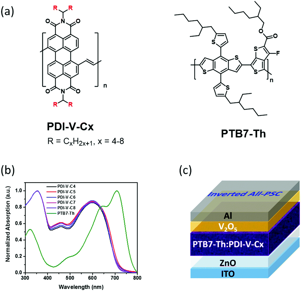 | ||
| Fig. 1 (a) Chemical structures of polymeric acceptors PDI-V-Cx (x = 4–8) and donor PTB7-Th. (b) Normalized absorption spectra of PDI-V-Cx and PTB7-Th in thin films. (c) The inverted all-PSC device structure used in the current study. | ||
Results and discussion
Synthesis and characterization
All polymers of PDI-V-Cx were synthesized via Stille reactions between trans-1,2-bis(tri-n-butylstannyl)ethylene and the corresponding dibromo-PDI monomers, PDI-Br2-Cx, with varied alkyl side chain lengths. Regio-isomer mixtures of PDI-Br2-Cx (with a 1,6-/1,7-dibromo- molar ratio of ca. 1![[thin space (1/6-em)]](https://www.rsc.org/images/entities/char_2009.gif) :4, according to 1H NMR spectroscopy)30 were used in the polymerization reactions to afford the corresponding regio-irregular polymers. More synthesis details can be found in the ESI.† Due to the “dove-tailed” alkyl side chains on PDI, all PDI-V-Cx exhibited adequate solubility in common organic solvents, including o-dichlorobenzene (DCB), chlorobenzene (CB) and chloroform. The number-average molecular weights (Mn) of the polymer series were measured with gel permeation chromatography (GPC) in 1,2,4-trichlorobenzene at an elevated temperature of 150 °C, and the data are summarized in Table 1. The results show that all polymers of PDI-V-Cx with different side chains showed similar Mn and polydispersity (Mw/Mn), which excluded significant device performance variations caused by molecular weight differences.
:4, according to 1H NMR spectroscopy)30 were used in the polymerization reactions to afford the corresponding regio-irregular polymers. More synthesis details can be found in the ESI.† Due to the “dove-tailed” alkyl side chains on PDI, all PDI-V-Cx exhibited adequate solubility in common organic solvents, including o-dichlorobenzene (DCB), chlorobenzene (CB) and chloroform. The number-average molecular weights (Mn) of the polymer series were measured with gel permeation chromatography (GPC) in 1,2,4-trichlorobenzene at an elevated temperature of 150 °C, and the data are summarized in Table 1. The results show that all polymers of PDI-V-Cx with different side chains showed similar Mn and polydispersity (Mw/Mn), which excluded significant device performance variations caused by molecular weight differences.
| Polymer | M n (kDa) | M w/Mn |
E
optga (eV) |
LUMOb (eV) | HOMOc (eV) | E-mobilityd (cm2 V−1 s−1) |
|---|---|---|---|---|---|---|
| a Optical bandgap obtained in the film state. b Measured with cyclic voltammetry. c Estimated from (LUMO − Eoptg). d Calculated using the SCLC model. | ||||||
| PDI-V-C4 | 13.4 | 2.03 | 1.73 | −4.04 | −5.77 | 1.2 × 10⁻³ |
| PDI-V-C5 | 13.4 | 1.96 | 1.72 | −4.04 | −5.76 | 1.1 × 10⁻³ |
| PDI-V-C6 | 15.1 | 2.03 | 1.73 | −4.03 | −5.76 | 1.9 × 10⁻³ |
| PDI-V-C7 | 13.7 | 2.23 | 1.73 | −4.02 | −5.75 | 2.7 × 10⁻³ |
| PDI-V-C8 | 15.2 | 2.08 | 1.73 | −4.04 | −5.77 | 1.1 × 10⁻³ |
Optical and electrochemical properties
On the basis of the UV-vis absorption spectra of the thin films (Fig. 1b), the five polymer acceptors exhibited almost identical absorption properties, suggesting that the intrinsic electronic properties governed by the polymer backbone were nearly unaffected by the variation in the alkyl side chain length. Similarly, the lowest unoccupied molecular orbitals (LUMOs) and highest occupied molecular orbitals (HOMOs) of PDI-V-Cx, which were determined by cyclic voltammetry to be approximately −4.03 eV and −5.76 eV, respectively, also showed minimal changes with the side chain length (Fig. S2, ESI†). In addition, the space-charge-limited-current (SCLC) method with a device structure of ITO/ZnO/PDI-V-Cx/Ca/Al was applied to examine the electron transport properties of PDI-V-Cx in the neat thin-film state. All PDI-V-Cx exhibit electron mobilities (μe) of over 1 × 10⁻³ cm2 V−1 s−1 (Table 1), comparable to those of fullerene derivatives, such as PCBM. Among all the different polymers, PDI-V-C7 shows the highest μe value, followed by PDI-V-C6, whereas the other three polymers having either longer or shorter side chains display slightly lower electron mobilities.Photovoltaic properties
The effects of alkyl side chain length in the acceptor polymers on the photovoltaic properties were then investigated by examining the all-PSC device performance. Bulk-heterojunction (BHJ) devices containing PDI-V-Cx as the acceptor and PTB7-Th as the donor were fabricated with an inverted device structure of ITO/ZnO/PTB7-Th:PDI-V-Cx/V2O5/Al. The active layer was spin-cast from a solution of CB with a D/A weight ratio of 1:1. Measurements of the device performance were carried out under the illumination of AM 1.5 simulated solar light at 100 mW cm−2. The J–V curves are shown in Fig. 2a, and the corresponding parameters are summarized in Table 2. In general, as both branches in the alkyl side chains are extended from 4 to 8 carbons, both Jsc and FF values are found to increase first before decreasing with chain length. As the Voc remains nearly constant over the entire range of examined side chain length, such variations in Jsc and FF naturally lead to a similar trend in the variation of average PCE, as the polymer side chain differs. In particular, among all examined devices, those comprising the active layers of PTB7-Th:PDI-V-C6 and PTB7-Th:PDI-V-C7 display Jsc values of 15.55 and 15.30 mA cm−2, respectively, which are evidently higher than those observed with the other three acceptors. Meanwhile, higher FF values ranging from 0.63 to 0.65 are obtained for PDI-V-C6/C7/C8, which are considerably higher than those for PDI-V-C4/C5. Overall, the polymers PDI-V-C7 and PDI-V-C6 provide better device performance than the other three acceptors bearing either longer or shorter side chains. The best average PCE of 7.40% is achieved with PTB7-Th:PDI-V-C7, which is slightly higher than the PCE of PTB7-Th:PDI-V-C6 devices (Table 2). Similar to the results shown in our previous work,15 the presence of various solvent additives, such as 1,8-diiodooctane and 1-chloronaphthalene, resulted in lowered PCEs for PTB7-Th:PDI-V-C7 (Table S1, ESI†). The fact that optimal device performance can be achieved without additives or post-treatments presents a great advantage for large-scale production.
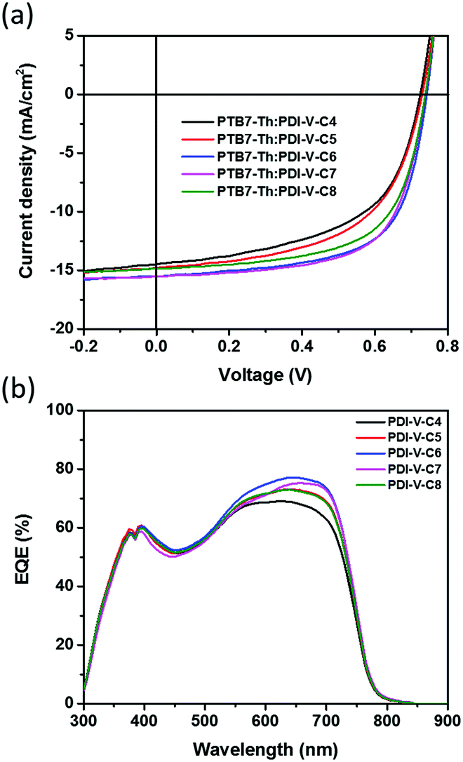 | ||
| Fig. 2 (a) J–V curves and (b) EQE spectra of all-PSCs comprising the active layer of PTB7-Th:PDI-V-Cx. | ||
| Blends | V oc (V) | J sc (mA cm−2) | FF | PCEa (%) | μ e (cm2 V−1 s−1) | μ h (cm2 V−1 s−1) | μ h/μe |
|---|---|---|---|---|---|---|---|
| a Data averaged over 10 cells, with the highest value shown in brackets. | |||||||
| PTB7-Th:PDI-V-C4 | 0.73 ± 0.01 | 14.44 ± 0.23 | 0.53 ± 0.03 | 5.58 ± 0.17 (5.75) | 0.8 × 10⁻⁴ | 6.9 × 10⁻⁴ | 8.6 |
| PTB7-Th:PDI-V-C5 | 0.73 ± 0.01 | 14.88 ± 0.17 | 0.55 ± 0.02 | 5.97 ± 0.13 (6.06) | 1.5 × 10⁻⁴ | 8.3 × 10⁻⁴ | 5.5 |
| PTB7-Th:PDI-V-C6 | 0.74 ± 0.01 | 15.55 ± 0.23 | 0.63 ± 0.02 | 7.25 ± 0.20 (7.38) | 1.8 × 10⁻⁴ | 7.6 × 10⁻⁴ | 4.2 |
| PTB7-Th:PDI-V-C7 | 0.74 ± 0.01 | 15.30 ± 0.07 | 0.65 ± 0.01 | 7.40 ± 0.06 (7.44) | 2.4 × 10⁻⁴ | 1.0 × 10⁻³ | 4.2 |
| PTB7-Th:PDI-V-C8 | 0.74 ± 0.01 | 14.83 ± 0.12 | 0.63 ± 0.03 | 6.91 ± 0.10 (6.99) | 2.1 × 10⁻⁴ | 1.1 × 10⁻³ | 5.2 |
The external quantum efficiency (EQE) was measured to compare the spectral response of different acceptors. As shown in Fig. 2b, devices containing different acceptors all exhibit a wide photo-responsive range of 300 to 800 nm, illustrating that both the donor and acceptor contribute to light harvesting in these all-PSCs. The maximum EQE values of the different devices all reach over 69%, and the variation of the maximum EQE is well correlated with the changes in Jsc values observed with different acceptors. The photocurrent values calculated from the EQE spectra are also found to be consistent with the Jsc values obtained from the J–V measurements of the corresponding acceptors, showing differences of less than 4% (see Table S2, ESI†).
Further insight into the relationship between the polymer structure and device performance was gained by measuring the hole (μh) and electron mobility (μe) of the polymer blends using the SCLC method. As shown in Table 2, the bulk charge carrier transport properties of the active layer blends are generally consistent with the observed photovoltaic properties, especially with the FF values. Among all fabricated devices, the PTB7-Th:PDI-V-C7 blend shows the highest μe and the most balanced μh/μe, suggesting rapid charge transport and efficient charge extraction with minimized charge recombination within this polymer blend.31–33 The combination of these effects results in the highest FF and highest PCE values at this side chain length.
Photoluminescence (PL) quenching experiments of the polymer blend films were also performed to assess the percentage of excitons that can reach and dissociate at the donor/acceptor interface (Fig. S3, ESI†). Blending PDI-V-C7 with PTB7-Th results in fluorescence quenching of about 95% compared with the neat PDI-V-C7 films, indicating highly efficient photo-induced charge transfer between PTB7-Th and PDI-V-C7 in the blend film. In general, the quenching efficiencies of the different blends are found to be similar in the range of 93–95% (Fig. S3a, ESI†).
Morphology
Atomic force microscopy (AFM) imaging of the BHJ films provides information on the surface morphology of the active layers in the all-PSCs. AFM height and phase images with a scan area of 1 μm × 1 μm are shown in Fig. 3. Generally, the root-mean-square (RMS) roughness of all the blends decreased initially and then increased with the increasing side-chain length of PDI-V-Cx, and the RMS roughness differences among the PDI-V-C6, PDI-V-C7 and PDI-V-C8 blends are very small. Relatively smooth and uniform surface morphologies with comparable domain sizes (∼20 nm) are observed for the three polymers with longer side chains, which reasonably accounts for their superior photovoltaic performance. In contrast, blends of the donor material with PDI-V-C5 and PDI-V-C4 both show noticeably higher RMS roughness and larger domain sizes (ca. 60–100 nm). The extra-large domain size hinders efficient exciton collection and dissociation at the interfaces, resulting in lower Jsc. The AFM characterization thus clearly reveals that the less optimal device performances of PDI-V-C4 and PDI-V-C5 are the results of their less favourable phase separation of the polymer blends. Their larger domains are presumably caused by the shorter alkyl chain lengths of PDI-V-C4 and PDI-V-C5, giving rise to higher self-aggregation propensity of the acceptor and low miscibility with the donor polymer. | ||
| Fig. 3 AFM height (upper) and phase (lower) images of the blend films (1 μm × 1 μm) of PTB7-Th:PDI-V-C4 (a and f); PTB7-Th:PDI-V-C5 (b and g); PTB7-Th:PDI-V-C6 (c and h); PTB7-Th:PDI-V-C7 (d and i); and PTB7-Th:PDI-V-C8 (e and j). | ||
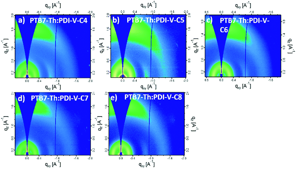
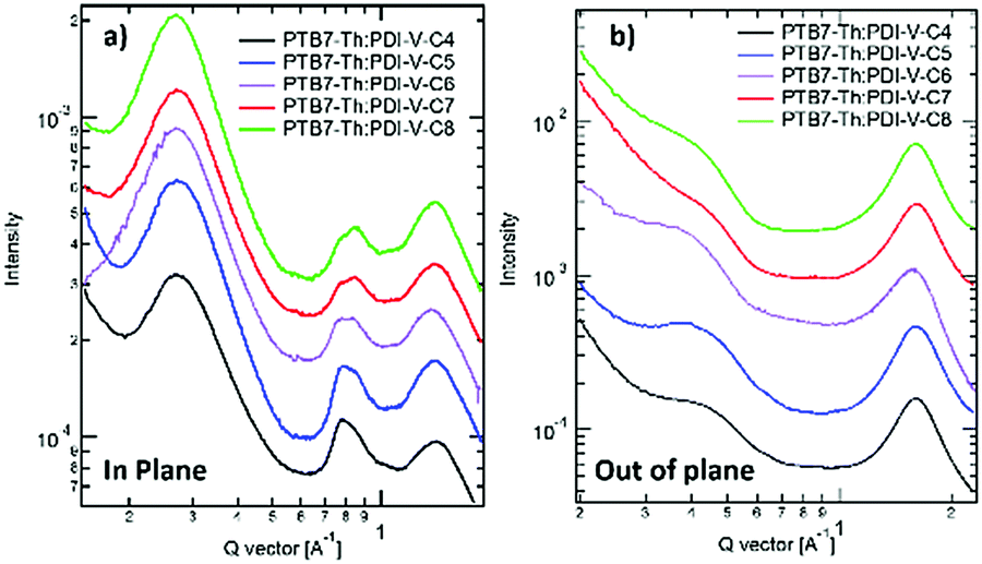
To understand the effect of side-chain length manipulation on molecular packing and device performance, GIWAXS34 measurements were carried out. The 2-D GIWAXS patterns and 1-D scattering profiles for neat PDI-V-C4-8 films are provided in Fig. 4 and 5, respectively. It is clear that all films have relatively low crystallinity, which is evident from the absence of higher order lamellar peaks in both the in-plane (IP) and out-of-plane (OOP) directions. The (100) lamellar peak is observed at a different q in the IP and OOP directions especially in PDI-V-C4 and PDI-V-C5, with an oval shape (100) signal in the 2D pattern. The difference between the IP and OOP (100) peak is reduced with an increased side-chain length. This is readily noticeable as the oval feature becomes more circular with increasing side-chain length. The IP lamellar spacing is reduced (from 23.4 Å to 22.6 Å) and the OOP lamellar spacing is increased (from 13.7 Å to 15.5 Å) with increasing side-chain length, especially from PDI-V-C5 to PDI-V-C6. Moreover, a (001) peak is present in all neat PDI-V-Cx films at q = 0.76–0.80 Å−1. This indicates that the polymer backbone direction is predominantly in the plane of the film. A relatively sharp feature is observed at q = 0.26 Å−1 and q = 0.25 Å−1 in the PDI-V-C4 and PDI-V-C5, respectively, and not in any of the other films. It is not entirely clear what these features are due to, but it is worth noting that the devices based on these two films have significantly lower FFs than those with the other films. It is possible that these features correspond to a polymorph with less interdigitated lamellar-packing. Further investigation is necessary to fully elucidate the nature of these features. The (010) peak in the OOP direction without a clear corresponding IP (100) signature indicates a preferential “rolling-log”, 2D orientation distribution in all five neat films. Increasing the side-chain length appears to also increase the (010) OOP spacing from 3.9 Å to 4.2 Å.
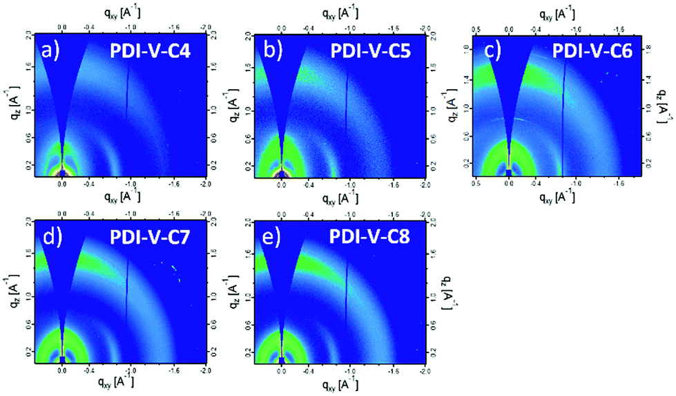 | ||
| Fig. 4 2-D GIWAXS patterns of neat PDI-V-Cx films: (a) PDI-V-C4, (b) PDI-V-C5, (c) PDI-V-C6, (d) PDI-V-C7 and (e) PDI-V-C8. | ||
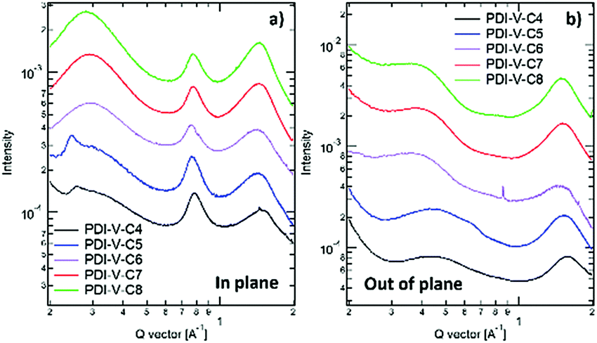 | ||
| Fig. 5 1-D GIWAXS profiles of neat PDI-V-Cx films: (a) in-plane and (b) out-of-plane. | ||
When blending PTB7-Th with PDI-V-Cx, we observe mostly similar morphological features to the neat PDI-V-Cx films as shown in Fig. 6 and 7. However, an important difference in the neat films is the appearance of two peaks at ∼0.8 Å−1. The lower q peak corresponds to the (001) peak of PDI-V-Cx and the second peak is attributed to a (001) peak of PTB7-Th (see Fig. S4, ESI†). It is noticeable that as the side chain length increases, the PDI-V-Cx (001) peak weakens and the intensity of the second peak increases. This suggests that the in-plane stacking order of the PDI-V-Cx backbone is distorted as the side-chain length is extended. Meanwhile, the backbone ordering of PTB7-Th is improved. The coherence length and the d-spacing in the π–π (010) direction are similar for all blend films, which are not substantially influenced by varying the side-chain length. However, correlations between the (100) peak of the neat PDI-V-Cx films and FF and Jsc can help illuminate some structure-performance dependence. As the side-chain length is increased the lamellar spacing in the IP direction is decreased and the OOP lamellar spacing is increased. The OOP lamellar spacing positively correlates with an increase in Jsc and FF. This can be attributed to better OOP charge transport along the thickness of the film, which is beneficial in a solar cell architecture. This is in agreement with the positive correlations between both electron and hole mobilities and OOP lamellar spacing. While it is more relevant to look at these features in the blend films, the scattering profiles of the lamellar and π–π stacking for PTB7-Th largely overlap with those for PDI-V-Cx, making it challenging to isolate each of the components’ morphological evolution separately in the blends.
 | ||
| Fig. 6 2-D GIWAXS patterns of PTB7-Th:PDI-V-Cx blend films: (a) PTB7-Th:PDI-V-C4, (b) PTB7-Th:PDI-V-C5, (c) PTB7-Th:PDI-V-C6, (d) PTB7-Th:PDI-V-C7 and (e) PTB7-Th:PDI-V-C8. | ||
 | ||
| Fig. 7 1-D GIWAXS profiles of PTB7-Th:PDI-V-Cx blend films: (a) in-plane and (b) out-of-plane. | ||
Conclusions
In summary, the effects of alkyl side chains of perylenediimide vinylene (PDI-V) polymeric acceptors on the performance of all-PSCs are studied. With PTB7-Th incorporated as the donor material for all the examined devices, a series of all-PSCs were fabricated using polymers PDI-V-Cx with different alkyl side-chain length as the acceptor. It is found that, while minimum change is detected in Voc, both Jsc and FF show a clear trend of first increasing and then decreasing with the alkyl side chain length extension. GIWAXS results show, among other correlations, that the IP lamellar spacing is decreased and the OOP lamellar spacing is increased with increasing side-chain length. Moreover, increasing the side-chain length increases the OOP (010) π–π spacing in the neat PDI-V-Cx films. All these trends correlate well with Jsc and FF, suggesting the beneficial effects of improved OOP charge transport for the device performance. While molecular packing parameters show complex correlations with the device performance parameters, an optimal morphology seems to have been met in PTB7-Th:PDI-V-C7, offering the highest PCE among all studied polymer acceptor analogues. Consistently, PDI-V-C7 showed superior charge transport properties in both neat films and blend materials. Our study demonstrated the effects of varying the side-chain length in the polymer acceptor in optimizing the performance of all-PSCs. In conjunction with the previously observed need to optimize side chains of donors in fullerene-based blends,23,24 our results indicate that side chains need to be optimized irrespective of whether a polymer serves as a donor or acceptor. Given the complex formation of an all-PSC morphology, it is conceivable that there is a kinetic or thermodynamic interaction between donors and acceptors and that more extensive side-chain studies are required to fully optimize all-PSCs.Experiments
Device fabrication and characterization
Pre-patterned ITO-coated glass with a sheet resistance of ∼15 Ω per square was used as the substrate. The substrates were cleaned by sequential cycles of sonication in soap water, deionized water, acetone, and isopropanol for 15 min each. After UV/ozone treatment for 60 min, ZnO electron transport layers were prepared on top of the ITO by spin-coating a ZnO precursor solution (diethyl zinc) at 5000 rpm. The active-layer solutions were prepared in CB (with a polymer concentration of 9 mg mL−1 and a D/A ratio at 1:1). To completely dissolve the polymers, the solutions were stirred on a hot plate at 110 °C for at least 3 hours. The active layers were spin-coated from the cooled polymer solution on the ZnO coated substrates in a glove-box under an N2 atmosphere at 1700 rpm to obtain a thickness of ∼120 nm. The blend films were then transferred to a vacuum chamber of a thermal evaporator in the same glove-box. At a vacuum level of ≤3 × 10⁻⁶ Torr, a thin layer (∼7 nm) of V2O5 was deposited as the anode interlayer, followed by the deposition of 100 nm of Al as the top electrode. All cells were encapsulated using epoxy inside the glove-box. The device J–V characteristics were measured under AM 1.5G (100 mW cm−2) using a Newport solar simulator. The light intensity was calibrated using a standard Si diode (with a KG5 filter purchased from PV Measurement) to bring spectral mismatch to unity. The J–V characteristics were recorded using a Keithley 2400 source meter unit. Typical cells have a device area of 5.9 mm2, which is defined by a metal mask with an aperture aligned with the device area. EQEs were measured using a Newport EQE system equipped with a standard Si diode. Monochromatic light was generated from a Newport 300 W lamp source.
Acknowledgements
This work at Peking University is supported by the National Natural Science Foundation of China (No. 21674001 and 51473003). We thank Hong Kong Innovation and Technology Commission for the support through ITC-CNERC14SC01. O. A. and H. A. acknowledge a UNC-GA Research Opportunity Initiative grant. X-ray data were acquired at beamline 7.3.3 at the Advanced Light Source, which is supported by the Director, Office of Science, Office of Basic Energy Sciences, of the U.S. Department of Energy under Contract No. DE-AC02-05CH11231. L. Ye and J. Kim are acknowledged for assisting with the measurements and data acquisition. E. Schaible, and C. Zhu are acknowledged for help with X-ray experimental setup and maintenance of the beamline.Notes and references
- A. Facchetti, Mater. Today, 2013, 16, 123 CrossRef CAS.
- Y. Zhou, T. Kurosawa, W. Ma, Y. Guo, L. Fang, K. Vandewal, Y. Diao, C. Wang, Q. Yan, J. Reinspach, J. Mei, A. L. Appleton, G. I. Koleilat, Y. Gao, S. C. B. Mannsfeld, A. Salleo, H. Ade, D. Zhao and Z. Bao, Adv. Mater., 2014, 26, 3767 CrossRef CAS PubMed.
- Y. Zhou, Q. Yan, Y. Q. Zheng, J. Y. Wang, D. Zhao and J. Pei, J. Mater. Chem. A, 2013, 1, 6609 CAS.
- C. Lee, H. Kang, W. Lee, T. Kim, K. H. Kim, H. Y. Woo, C. Wang and B. J. Kim, Adv. Mater., 2015, 27, 2466 CrossRef CAS PubMed.
- D. Mori, H. Benten, I. Okada, H. Ohkita and S. Ito, Energy Environ. Sci., 2014, 7, 2939 CAS.
- Y. Diao, Y. Zhou, T. Kurosawa, L. Shaw, C. Wang, S. Park, Y. Guo, J. A. Reinspach, K. Gu, X. Gu, B. C. K. Tee, C. Pang, H. Yan, D. Zhao, M. F. Toney, S. C. B. Mannsfeld and Z. Bao, Nat. Commun., 2015, 6, 7955 CrossRef CAS PubMed.
- T. Kim, J. H. Kim, T. E. Kang, C. Lee, H. Kang, M. Shin, C. Wang, B. Ma, U. Jeong, T. S. Kim and B. J. Kim, Nat. Commun., 2015, 6, 8547 CrossRef CAS PubMed.
- Y. Liu, J. Zhao, Z. Li, C. Mu, W. Ma, H. Hu, K. Jiang, H. Lin, H. Ade and H. Yan, Nat. Commun., 2014, 5, 5293 CrossRef CAS PubMed.
- S. H. Liao, H. J. Jhuo, P. N. Yeh, Y. S. Cheng, Y. L. Li, Y. H. Lee, S. Sharma and S. A. Chen, Sci. Rep., 2014, 4, 6813 CrossRef CAS PubMed.
- J. W. Jung, F. Liu, T. P. Russell and W. H. Jo, Energy Environ. Sci., 2012, 5, 6857 CAS.
- J. Huang, J. H. Carpenter, C. Z. Li, J. S. Yu, H. Ade and A. K. Y. Jen, Adv. Mater., 2016, 28, 967 CrossRef CAS PubMed.
- J. Zhao, Y. Li, G. Yang, K. Jiang, H. Lin, H. Ade, W. Ma and H. Yan, Nat. Energy, 2016, 1, 15027 CrossRef CAS.
- S. Zhang, L. Ye, W. Zhao, B. Yang, Q. Wang and J. Hou, Sci. China: Chem., 2015, 58, 248 CrossRef CAS.
- L. Gao, Z. Zhang, L. Xue, J. Min, J. Zhang, Z. Wei and Y. Li, Adv. Mater., 2016, 28, 1884 CrossRef CAS PubMed.
- Y. Guo, Y. Li, O. Awartani, J. Zhao, H. Han, H. Ade, D. Zhao and H. Yan, Adv. Mater., 2016, 28, 8483 CrossRef CAS PubMed.
- Z. Li, X. Xu, W. Zhang, X. Meng, W. Ma, A. Yartsev, O. Inganäs, M. R. Andersson, R. A. J. Janssen and E. Wang, J. Am. Chem. Soc., 2016, 138, 10935 CrossRef CAS PubMed.
- Y. J. Hwang, B. A. E. Courtright, A. S. Ferreira, S. H. Tolbert and S. A. Jenekhe, Adv. Mater., 2015, 27, 4578 CrossRef CAS PubMed.
- T. Lei, J. Dou and J. Pei, Adv. Mater., 2012, 24, 6457 CrossRef CAS PubMed.
- T. Kurosawa, Y. Chiu, Y. Zhou, X. Gu, W. Chen and Z. Bao, Adv. Funct. Mater., 2016, 26, 1261 CrossRef CAS.
- X. Guo, H. Xin, F. S. Kim, A. D. T. Liyanage, S. A. Jenekhe and M. D. Watson, Macromolecules, 2011, 44, 269 CrossRef CAS.
- J. Lee, M. Kim, B. Kang, S. B. Jo, H. G. Kim, J. Shin and K. Cho, Adv. Energy Mater., 2014, 4, 1400087 CrossRef.
- L. Fang, Y. Zhou, Y. X. Yao, Y. Diao, W. Y. Lee, A. L. Appleton, R. Allen, J. Reinspach, S. C. B. Mannsfeld and Z. Bao, Chem. Mater., 2013, 25, 4874 CrossRef CAS.
- W. Li, K. H. Hendriks, A. Furlan, W. S. C. Roelofs, S. C. J. Meskers, M. M. Wienk and R. A. J. Janssen, Adv. Mater., 2014, 26, 1565 CrossRef CAS PubMed.
- J. H. Kim, S. Wood, J. B. Park, J. Wade, M. Song, S. C. Yoon, I. H. Jung, J. S. Kim and D. H. Hwang, Adv. Funct. Mater., 2016, 26, 1517 CrossRef CAS.
- C. Kästner, C. Ulbricht, D. A. M. Egbe and H. Hoppe, J. Polym. Sci., Part B: Polym. Phys., 2012, 50, 1562 CrossRef.
- Y. Hwang, T. Earmme, S. Subramaniyan and S. A. Jenekhe, Chem. Commun., 2014, 50, 10801 RSC.
- J. W. Jung, J. W. Jo, C. C. Chueh, F. Liu, W. H. Jo, T. P. Russell and A. K. Y. Jen, Adv. Mater., 2015, 27, 3310 CrossRef CAS PubMed.
- W. Lee, C. Lee, H. Yu, D. J. Kim, C. Wang, H. Y. Woo, J. H. Oh and B. J. Kim, Adv. Funct. Mater., 2016, 26, 1543 CrossRef CAS.
- S. Zhang, L. Ye and J. Hou, Adv. Energy Mater., 2016, 6, 1502529 CrossRef.
- X. Zhang, C. Zhan, X. Zhang and J. Yao, Tetrahedron, 2013, 69, 8155 CrossRef CAS.
- T. Earmme, Y. Hwang, S. Subramaniyan and S. A. Jenekhe, Adv. Mater., 2014, 26, 6080 CrossRef CAS PubMed.
- C. Mu, P. Liu, W. Ma, K. Jiang, J. Zhao, K. Zhang, Z. Chen, Z. Wei, Y. Yi, J. Wang, S. Yang, F. Huang, A. Facchetti, H. Ade and H. Yan, Adv. Mater., 2014, 26, 7224 CrossRef CAS PubMed.
- B. Qi and J. Wang, Phys. Chem. Chem. Phys., 2013, 15, 8972 RSC.
- A. Hexemer, W. Bras, J. Glossinger, E. Schaible, E. Gann, R. Kirian, A. MacDowell, M. Church, B. Rude and H. Padmore, J. Phys.: Conf. Ser., 2010, 247, 012007 CrossRef.
Footnote |
| † Electronic supplementary information (ESI) available: Material syntheses and additional characterization data. See DOI: 10.1039/c6qm00355a |
| This journal is © the Partner Organisations 2017 |