
 Open Access Article
 This Open Access Article is licensed under a
 Creative Commons Attribution 3.0 Unported Licence
Layered 2D material heterostructures – a colloidal perspective
Eric H.
Hill
 ab
ab
aInstitute of Physical Chemistry, University of Hamburg, Grindelallee 117, 20146 Hamburg, Germany. E-mail: eric.hill@chemie.uni-hamburg.de
bThe Hamburg Center for Ultrafast Imaging (CUI), Luruper Chausee 149, 22761 Hamburg, Germany
First published on 1st July 2024
Abstract
The development and ongoing discovery of 2D materials and their emergent optical and electronic properties have led to intense interest in the stacking of different 2D materials into layered heterostructures. While the initial efforts focused on mechanical transfer of 2D materials and vapor-phase epitaxial growth, there is an increasing body of research on colloidal methods for the fabrication of layered heterostructures. This review gives insight into the history and development of layered heterostructures composed of stacked 2D materials, starting from the origins of 2D materials research and leading up to the current state-of-the-art methods for fabricating 2D material heterostructures. Particular attention is given to colloidal approaches, with emphasis on the importance of surface chemistry in controlling both the assembly of dispersed 2D materials and direct colloidal synthesis at 2D material interfaces to achieve well-defined heterostructures. Approaches from diverse fields of chemistry such as the synthesis of 2D Janus nanosheets, modification of interlayer spaces of 2D materials, and colloidal atomic layer deposition give insight into potential future colloidal strategies. In summary, this review provides an overview of the basics of 2D material heterostructures and their fabrication, while also suggesting future colloidal avenues for the development of hybrid nanomaterials which would greatly benefit applications in (photo)catalysis, energy storage, sensing, optoelectronics, and more.
 Eric H. Hill | Eric H. Hill studied chemistry at Southern Oregon University (2009), and completed his doctorate under David Whitten and Debi Evans at the University of New Mexico (2014). He joined the group of Luis Liz-Marzán at CIC-biomaGUNE in Donostia/San-Sebastian, Spain, as a postdoc from 2015 to 2017, followed by a brief postdoc with Yuebing Zheng at UT Austin. He moved to Hamburg, Germany, in 2018 as a MOPGA-GRI fellow funded by the DAAD/BMBF to start his group. He joined the Cluster of Excellence CUI:AIM at the University of Hamburg as a “Young Investigator Research Group Leader” in 2020, where his group currently focuses on colloidal synthesis and assembly of nanomaterials. |
1. Background
In order to clarify the state of the art of colloidal 2D material heterostructures, a brief history of the development of 2D materials and an overview of some of the different materials is given (Section 1.1), followed by a short overview of 2D material heterostructures and some of their unique properties (Section 1.2).1.1. 2D materials
The discovery of two dimensional (2D) materials such as graphene and MoS2 has led to an explosion in interest in the field, which has since led to the discovery and development of a broad variety of 2D and ultrathin materials.1–4 In general, the composition and structure of 2D materials are the same as those of their parent bulk compounds, while their thickness ranges from 0.3 nm (e.g. graphene) to 2.8 nm (e.g. Bi2Sr2CaCu2Ox).1,2,4–7 In particular, semiconductors and the unique physical and electronic properties which arise from the confinement of their dimensions to nanometer-thick layers have led to 2D materials attracting intense interest. This is particularly notable for graphene, single-atomic layer thick sheets that, when stacked, compose graphite, which have generated intense interest since their discovery.8 The theory of graphene was first developed by Wallace in 1947 to better describe the electronic properties of graphite,9 and the first electron microscopy studies of thin graphite samples were reported from 1948 to 1962.10,11 While the first reliable observations of graphene by electron microscopy were made in 2001,12 Novoselov, Geim, and co-workers were the first to properly isolate and characterize graphene in 2004,13 which led to their 2010 Nobel Prize in Physics.Although graphene is generally seen as the first 2D material, even before its discovery numerous researchers had explored layered metal oxides, finding that they could be exfoliated into unilamellar 2D crystals by using colloidal processes such as ion-exchange and osmotic swelling.14–19 MoS2, a transition metal dichalcogenide (TMD), was also of significant interest to researchers decades before graphene. The “Scotch tape technique” of mechanical exfoliation (which was later used for the production of graphene in the landmark study by Novoselov et al.) was first reported for the production of few-layer MoS2 in 1965,20 whereas the liquid-phase exfoliation (LPE) of MoS2via lithium ion intercalation resulting in “one-molecule-thick sheets” was reported in 1986.20 Despite these early observations, it was the intense interest generated by graphene and the wide range of methods developed for related research that sparked renewed interest in MoS2 and other 2D materials for their unique optical, electronic and mechanical properties.21–24 The discrete, quantized electronic structure of 2D materials including graphene and TMDs has led to the discovery of numerous unique electronic and magnetic effects, such as highly tunable bandgaps which can be tuned from indirect to direct,23–25 enhanced photoluminescence,23,26 and coupling of spin and valley physics for “spintronic” and “valleytronic” devices.27–30
2D or ultrathin materials comprise a broad range of different materials. They can vary in thickness, from single atom-thick layers in materials including graphene, g-C3N4, and h-BN, to periodic stacks of varying thickness, depending on the crystal structure. Non-layered materials can also exhibit interesting physical, optical, or electronic properties when deposited or grown as layers with nanometric thickness, particularly plasmonic metals31,32 and semiconductors.33,34 A significant number of layered bulk solids have been discovered and studied for their potential in the formation of hybrid nanomaterials. Phyllosilicates are a broad class of materials composed of 2D sheets of tetrahedral and octahedral coordination, to which minerals pyrophyllite, muscovite, talc, montmorillonite, and others belong.35 As phyllosilicates in general tend to have a wide bandgap, high dielectric constant, and high thermal stability, they have recently found increased use in electronic and optoelectronic applications, as well as incorporation into different 2D material heterostructures.35 Misfit layer chalcogenides, with the formula (MX)1+m TX2 or (MX)1+m (TX2)2 (where M = Sn, Pb, Sb, Bi, rare earth elements; T = Ti, V, Cr, Nb, Ta; X = S, Se), consist of alternating stacks of MX and TX2 layers.36–38 These can consist of multilayered misfit compounds, which show various polytypes, and the potential for non-stoichiometry in the MX layers due to M atom vacancies. Some misfit layer chalcogenides demonstrate interesting electronic and magnetic properties such as superconductivity and antiferromagnetic ordering,37 which have found application in thermoelectric energy conversion in recent years.39 Aurivillius- and Sillén-Aurivillius-type perovskites consist of a layered structure in which Bi2O2 layers are sandwiched between (Am−1 Bm O3m+1) layers, where A is a 12-atom coordinated cation such as Na+, K+, Ca2+, Sr2+, Pb2+, Ba2+, Ln3+, Bi3+, etc., and B is a combination of cations suitable for octahedral coordination, e.g., Fe3+, Cr3+, Ti4+, Nb5+, Mo6+, etc.40 Aurivillius perovskites have shown great potential as naturally layered multiferroics,41 and for applications in photocatalytic water oxidation42 and overall water splitting.8
Recently, the discovery of novel classes of materials such as MXenes has further transformed the field,43–45 and the potential of machine learning and computational approaches to predict possible new 2D materials has further opened the door to almost unlimited potential new 2D materials.46 The advantages of MXenes, with the chemical formula MnXn+1T, where M is a transition metal, X is C or N, and T is a terminal group (generally –OH or –F), are manifold. First, the different possible combinations of M and X elements with n varying from 2 to 5 means that a huge number of MXenes are theoretically possible. Second, as the MAX phases used to derive MXenes are synthesized at temperatures exceeding 800 °C, they exhibit very high temperature stability,47 which leds to numerous applications at elevated temperatures and opens the door to processing techniques that might damage more thermally sensitive materials. Furthermore, many different possible terminal groups can be introduced during synthesis, which allows for tunable surface chemistry; although in practice, this can be challenging to achieve and greatly depends on the target MXene and the synthetic approach. Finally, MXenes generally display a negative surface charge, similar to clay-like materials, which allows for electrostatic-based assembly and surface modifications towards fabrication of layered heterostructures, which is discussed in detail below.
For this review, the materials of focus are semiconductors, as changes in their electronic structure due to confinement can lead to significant changes in their properties,23–25 making the understanding of their synthesis critical for advancing applications. These thickness-dependent changes in their properties can lead to reduced recombination of photogenerated electrons and holes, decrease of the bandgap, and increased photoluminescence, which are potentially advantageous for applications such as photocatalysis, photovoltaics, and optoelectronics. These unique properties, and the potential for synergy and enhancement when two 2D materials are combined, make 2D heterostructures an exciting research direction. More detailed discussion of different 2D materials and their unique properties can be found in a number of reviews.2,4,5,48–50
1.2. 2D material heterostructures
The wide range of different 2D materials and their unique properties can allow a plethora of interesting combinations in 2D heterostructures (Fig. 1a). Initial studies on VdW heterostructures, focused on graphene, showed that bilayers or multilayers of graphene with a certain twist angle between the two layers can exhibit new properties such as high carrier emission, topological superconductivity,51,52 and tunable photoluminescence.51,52 An angle as low as 1.1° between 2D layers significantly alters the electronic structure of the bilayer, leading to distinct energy and momentum states known as flat bands.51,52 In so-called magic-angle-twisted bilayer graphene, superconducting and topological insulating states have been recently observed.53–60 The twisting of the two layers leads to a distinct Moiré pattern,61,62 which leads to a certain periodicity in the distances between different lattice positions of the two layers.53,56,63–66 This has also been shown in transition metal dichalcogenides such as MoS2 and WS2 (Fig. 1b–e).67 The changes in relative lattice position can also be used to block carriers with a specific electron spin, known as spin filtering.68,69 | ||
| Fig. 1 (a) Examples of 2D materials, grouped by basal surface charge; (b) example of a 2D layered heterostructure of two TMDs, where the twist angle is shown; (c) micrograph of a MoS2/WSe2 heterostructure formed by mechanical transfer; (d) electron diffraction showing the offset of the two 2D crystals in the heterostructure; (e) transmission electron micrograph of single-layer MoS2 (SL MoS2) and MoS2/WSe2 heterostructures displaying the Moiré pattern due to the twist angle between layers. Panel (a) is adapted with permission from The American Chemical Society.7 Panels (b)–(e) are adapted with permission from the Proceedings of the National Academy of Sciences of the United States of America.67 | ||
While 2D materials in twisted layered structures are highly interesting for the reasons mentioned above and more,70 the development of 2D heterostructures, i.e., two ultrathin layers of different material compositions, has also led to significant advances in materials science and solid-state physics that have reverberated across various scientific fields. Layered heterostructures were first reported by Koma and co-workers in 1984, via the growth of NbSe2 thin films on 2H-MoS2.71,72 However, the majority of reports since then naturally stem from the graphene community, as this material was extensively studied following its report in the early 2000s. In that sense, mechanical exfoliation and transfer of one material followed by the sequential laying of an individual sheet of another material atop it was first reported by Dean et al. with graphene and hexagonal boron nitride (h-BN).73 A variety of different stepwise mechanical transfer methods similar to this have been reported since then, which are detailed in Section 2. The colloidal synthesis and exfoliation of 2D materials is critical for the development of colloidal assembly techniques, and thus this topic is briefly covered in Section 3. A number of other approaches based on the colloidal restacking of exfoliated nanosheets have also been reported, which are detailed in Section 4. There are a number of colloidal techniques to control the surface chemistry at the basal interfaces of 2D materials, and examples include Janus-functionalized nanosheets and the formation of clays “pillared” with surfactants and different metal oxides, which are detailed in Section 5. Finally, the state of the art in direct colloidal synthesis of 2D material heterostructures, particularly stepwise shell growth in semiconductor chalcogenide nanoplatelets and the synthesis of semiconductors in the interlayer space of layered material templates, is discussed in detail in Section 6.
2. Non-colloidal approaches to 2D material heterostructures
While the focus of this review is on the development of colloidal approaches for the fabrication of 2D material heterostructures, it is essential to first outline the “classic” approaches for fabricating well-defined 2D material heterostructures. These are generally recognized as the stepwise mechanical stacking of individual exfoliated sheets (Section 2.1), vapor-phase synthesis of 2D materials atop one another held together by VdW interactions (Section 2.2), and annealing of (typically amorphous) precursor layers at high temperatures (Section 2.3).2.1. Mechanical transfer
Mechanical transfer, i.e., the scotch tape method, is a classic and straightforward method to achieve 2D heterostructures, particularly van der Waals heterostructures, based on the stepwise mechanical transfer of individual exfoliated sheets atop one another on a substrate. This approach consists of two methods, known as carrier foil transfer and stamping, which are variations of the same basic approach depending on whether the first 2D layer can be transferred from the growth substrate or if it can be directly exfoliated onto the transfer layer. In carrier foil transfer, the 2D nanomaterial sheet is placed on a thin polymer film, generally PMMA or a thermal release tape, by either covering the 2D material with this transfer polymer or directly exfoliating the 2D sheet onto it (Fig. 2a). The 2D material sheet is then transferred atop this polymer layer to the desired substrate, and released from the film either by heating (when using thermal release tape),74 or by dissolving the layer with solvent (for polymers such as PMMA).75 There are numerous variations of this method, involving different types of polymers and methods for retrieving the heterostructure from liquid–air interfaces. However, due to the lack of mechanical stability of the polymer film which limits the capability to align the two layers, the involvement of solvents (some of which are chemically aggressive, such as KOH) which can damage more delicate 2D materials, and potentially poor-quality interfaces between the two sheets which is further complicated by the incomplete removal of the transfer polymer, other methods have been developed to achieve well-ordered 2D layered assemblies. | ||
| Fig. 2 Mechanical transfer of 2D materials: (a) carrier-foil transfer technique; (b) soft-lithography approach using the intermediate release layer; and (c) stamping of 2D materials atop one another via vdW interactions and transfer to a target substrate. | ||
Microcontact-printing-based approaches,76,77 otherwise referred to as stamping, use elastomeric stamps (composed of materials such as PDMS) to “pick up” a 2D material sheet to be stamped, and then by bringing the 2D-material-adhered stamp in contact with a substrate, the 2D material sheet is transferred to the substrate (Fig. 2b). While this method is very simple and allows for alignment due to the transparency of the elastomeric stamp, its success requires favorable adhesion between the stamp and the 2D material sheet, as well as slightly more-favorable interactions between the 2D sheet and the target substrate. Several variations of this method have been made, whereby different sacrificial polymer layers above or beneath the 2D material sheet can facilitate the transfer process by adjusting the adhesion properties between the different components.78–80 However, in some cases, the van der Waals-based assembly of 2D sheets into heterostructures is achievable without such sacrificial polymer layers, except for the top layer (Fig. 2c).80 As these techniques are not the focus of this review, the reader is pointed towards recent reviews if they are interested in learning more.81
2.2. van der Waals epitaxy
Much of the early research on 2D heterostructures stems from vapor-phase methods of 2D material growth. Known as van der Waals epitaxy (VdWE), this method results in the oriented in situ growth of 2D layers which gives rise to multilayer structures held together by weak VdW forces. Techniques suitable for VdWE include pulsed laser deposition (PLD) (Fig. 3a and b), molecular beam epitaxy (MBE) (Fig. 3c and d), and chemical vapor deposition (CVD).82–85 This was first reported in 1984 by Koma et al., demonstrating the epitaxial growth of NbSe2 on single-crystal MoS2 using molecular beam epitaxy.71,72,86 The weak VdW interactions between the crystalline layers of the 2D heterostructure is a defining feature which results in relaxed lattice matching conditions, allowing the fabrication of 2D–2D heterostructures with relatively large lattice mismatch (above 50%).86 In order to achieve such 2D heterostructures through VdWE in a well-controlled manner, compatibility with the substrate and non-catalytic growth processes that occur independent of the substrate are required. Non-catalytic CVD-based growth processes have been developed for a variety of materials, allowing the VdWE of diverse combinations of 2D materials such as graphene/h-BN,87 graphene/MoS2,88 SiC/MoS2,89 and a number of others, which have been covered in recent reviews.81 In general, the growth of epitaxial 2D layers via vapor-phase methods is governed by the chemical potential of the first adsorbed layers and strain at the interface, where strong surface adhesive forces between the adsorbate and substrate are ideal.90 | ||
| Fig. 3 (a) Schematic of PLD-based VdWE of WS2/WSe2 heterostructures; (b) scanning transmission electron microscopy image of 2D WS2/WSe2/WS2 heterostructures fabricated by PLD-based VdWE, with corresponding elemental mapping by electron-dispersive X-ray spectroscopy; (c) transmission electron microscopy image of 9 monolayer MoSe2 on highly oriented pyrolytic graphite (HOPG) fabricated by MBE. (d) Transmission electron microscopy image of multilayered WSe2 on single crystal Bi2Se3 fabricated by MBE. Panels (a) and (b) are adapted with permission from The American Chemical Society (CC-BY-NC-ND 4.0).91 Panels (c)92 and (d)93 are adapted with permission from IOP Publishing. | ||
One of the advantages of VdWE is the relative lack of impurities in the grown layers, due to fabrication using of high-purity source materials and ultra-high vacuum conditions (with pressures typically lower than 10−9 mTorr).94 There are also several drawbacks associated with this approach. First, the equipment requirements for the different techniques mentioned to carry out VdWE are significant, and typically expensive to obtain and maintain compared to colloidal approaches discussed in Sections 4 and 6. In addition, some materials such as TMDs (e.g., MoS2, WSe2, etc.) have high nucleation rates during their growth process, which ultimately limits the achievable grain sizes. For example, growth of TMDs by MBE generally suffers from a high nucleation rate, limiting the achievable grain size to 250 nm or below in most cases.95 This is partially due to low substrate temperatures that encourage nucleation, and maintaining a high substrate temperature has been shown to promote both metal and chalcogen desorption, limiting nucleation and increasing the size of grown TMDs. However, the increased desorption of precursors at the substrate interface also necessitates longer reaction times, although it results in TMD layers with order of magnitude larger grain sizes.82 In the case of h-BN, high temperature MBE has shown the most promise; however, while growth temperatures up to 1850 °C on graphite96 or 900–1000 °C on metal foils97–99 can be suitable for the formation of h-BN graphene heterostructures, these temperatures far exceed the decomposition temperatures of TMDs. Efforts have been made to achieve low-temperature epitaxial growth of h-BN/TMD heterostructures. While some success has been achieved using MBE at temperatures from 350–500 °C, the resulting 2D material layers are poorly crystalline.100 On the other hand, atomic layer deposition (ALD) has shown promising results for the growth of h-BN layers at temperatures as low as 275 °C;101,102 however, more work is needed in this direction to establish high-fidelity VdWE of h-BN/TMD heterostructures at growth temperatures typical of semiconductor/MEMS processing.
2.3. Reactive annealing
The annealing of amorphous or molecular precursors at high temperatures can result in the formation of distinct alternating 2D crystalline layers, enabling highly flexible design of complex superlattices based on compositionally diverse layered compounds. This was first shown by the group of Johnson et al., yielding a series of superlattices composed of mixed chalcogenides such as [NbSe2]6[TiSe2]6 and [(SnSe)1.16–1.09][(NbxMo1−x)Se2].103,104 These were achieved by first depositing amorphous precursors by physical vapor deposition, followed by an annealing step at elevated temperature to form kinetically trapped, metastable crystalline 2D layers which form a superlattice, albeit with some rotational disorder (Fig. 4a and b). Furthermore, the Schaak group has reported the synthesis of metastable 2D MBene nanosheet heterostructures via a room-temperature topotactic pathway.105 Starting with the stable compound MoAlB, room temperature chemical deintercalation of Al via NaOH etching provided MoAl1−xB, as a destabilized intermediate. After size-selecting the resulting grains to isolate the smallest (and thus most reactive) grains, they were annealed at 600 °C for 4.5 hours to further deintercalated Al and to crystallize metastable Mo2AlB2. Increasing this annealing time to 18 hours led to the formation of a layered heterostructure of alternating Mo2AlB2 and AlOx layers of 1–3 nm thickness (Fig. 4c).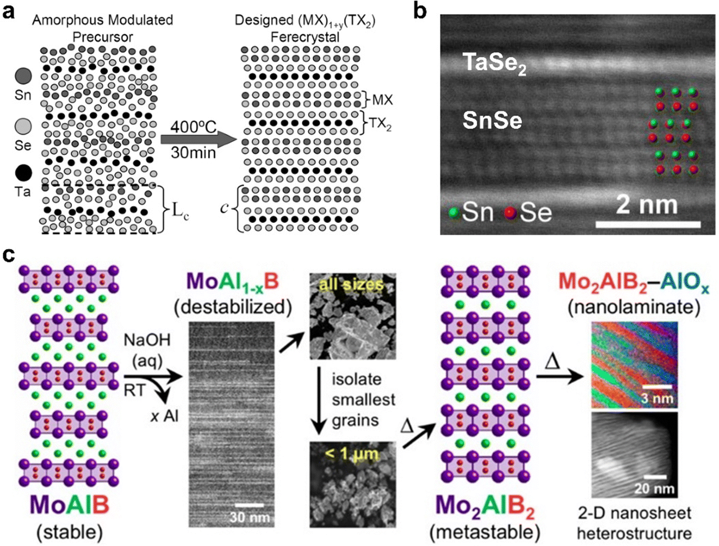 | ||
| Fig. 4 (a) Schematic of an as-deposited amorphous precursor on the left, and [(SnSe)1.15]1(TaSe2)1 which forms after annealing on the right; (b) cross-sectional high-resolution high angle annular dark field scanning transmission electron microscopy (HAADF-STEM) image of a [(SnSe)1.15]1(TaSe2)1 specimen, with layers noted and Sn and Se indicated with green and red beads, respectively; (c) scheme depicting the topotactic conversion of MoAlB to MoAl1−xB, followed by isolation of smaller grains and thermal annealing to achieve metastable Mo2AlB2 and finally a 2D nanosheet heterostructure composed of alternating Mo2AlB2 and AlOx layers of 1–3 nm thickness. Panels (a) and (b) are adapted with permission from The American Chemical Society,103 and panel (c) is reprinted with permission from the American Chemical Society.105 | ||
Although there is still much to explore in reactive annealing approaches, distinct advantages and disadvantages have already become apparent. The advantages of this technique are the scalability and quality of the interface between the two materials, which do not contain organic molecules or other contaminants. The approach is also relatively straightforward, although this depends on what is required to achieve the precursor materials prior to the annealing step. This strategy is not limited to 2D materials, and has also been applied to the formation of MoS2/WS2 heterostructured nanotubes, where the layer number and crystallinity of the MoS2 outer wall are controlled by synthetic conditions, yielding highly crystalline heterostructures with specific chirality.106 Considering the disadvantages, first of all, as this is not an epitaxial growth process, layer alignment out of plane cannot be controlled easily, which results in significant turbostratic disorder along the direction of layer stacking. This technique is also not applicable to all materials, and is mostly suitable for materials which have metastable intermediates or are capable of dealloying. Finally, this approach is potentially unsuitable for the preparation of colloidally stable heterostructures, unless it is possible to exfoliate the sheets via weak interactions between the layers.
3. Colloidal synthesis of 2D materials
In Section 2, methods which utilize mechanical assembly or vapor-phase/solid-state reactions to achieve the formation of 2D material heterostructures on solid substrates are described. Mechanical transfer approaches generally lead to good control over structure and interlayer coupling, although scalability is a concern. While vapor-phase approaches have shown great potential for 2D material heterostructures, they require complicated multi-step processes and expensive instrumentation in order to deposit well-defined crystalline layers by CVD or PVD. As the focus of this review is colloidal approaches to achieve 2D heterostructures, further information on surface-based approaches for 2D heterostructure fabrication can be found in recent reviews.81,107–110 To better understand the motivation behind colloidal approaches for fabricating 2D nanomaterial heterostructures, the common synthetic routes for colloidal 2D materials and their benefits and drawbacks are briefly discussed below.3.1. Brief overview of synthetic approaches
Colloidal methods for the synthesis of 2D materials have seen progressive improvements over the last decades, which allows for the facile and rapid synthesis of a large variety of 2D materials.107,111,112 These methods include solid-state synthesis (generally using high-temperature annealing of mixtures of powders in a tube furnace), and colloidal methods which are largely dominated by either hydrothermal, solvothermal, or “hot-injection” methods. Hydrothermal synthesis involves the dissolution of water-soluble precursors, generally some sort of shape/nucleation directing agents such as surfactants or polymers, and treatment at elevated temperatures (up to ∼220 °C) and pressures (up to ∼20 bar) in a Teflon beaker inside a sealed steel autoclave. Solvothermal methods bear great similarity to hydrothermal methods, except that solvents other than water, generally other polar protic solvents like ethylene glycol, polar aprotic, or nonpolar solvents, are used in place of water. While both approaches offer great flexibility and scalability, hydrothermal methods are generally more approachable due to the non-toxic, cheap, and safe nature of water as a solvent. In any case, the synthesis of 2D materials by either method requires intensive study in order to achieve both a well-defined structure and high monodispersity in the resulting product. Another method for the synthesis of 2D materials, which largely stems from the field of semiconductor nanoparticle synthesis, is known as “hot injection”, where precursors dissolved in nonpolar solvents are injected into a very hot (typical temperatures range from 200 to 350 °C) mixture of surfactant-like ligands in an organic solvent.113 Thus, numerous colloidal approaches to synthesize 2D nanomaterials via hydrothermal,111 solvothermal,114 and “hot-injection” methods have been reported,115 and future advances are still anticipated.111,112 Many 2D materials are synthesized in a layered form and must be exfoliated to achieve a dispersed, single-layer 2D material, a process discussed in greater detail in Section 3.2.3.2. Liquid-phase exfoliation of layered materials
Liquid-phase exfoliation is an important method for the production of large quantities of 2D materials, which has been developed to encompass a wide range of different materials.116–118 In general, LPE seeks to modify the nanosheet-liquid interactions to reduce the net exfoliation energy and stabilize the nanosheets against aggregation (Fig. 5). The majority of LPE approaches involve atleast one, and usually all, of the following steps: (1) exposure to strong ultrasonication or shear forces for extended durations; (2) surface chemistry modifications (e.g., TBA+, Li+, etc.) in order to assist the delamination process; (3) the use of surfactants and polymers in the dispersion, in order to stabilize the basal surfaces following delamination; and (4) the use of solvents with high boiling points and toxic health effects, such as N-methyl-2-pyrrolidone. While LPE is the most straightforward and widely used approach to achieve colloidal dispersions of 2D materials with concentrations even exceeding 1 g L−1,119 it also comes with its own set of drawbacks. | ||
| Fig. 5 (a) Schematic of ion-induced exfoliation of a charged layered crystal. Once osmotic swelling surpasses a threshold (critical bridge), the 2D layers can be completely exfoliated; (b) schematic of intercalation-based exfoliation; (c) schematic of ion-exchange-based intercalation, where smaller ions (red) are first exchanged with larger ions (yellow) prior to exfoliation aided by shear forces; and (d) schematic workflow for LPE: initial exfoliation leads to a broad size distribution, which can be narrowed through sequential centrifugation cycles. Panel (a) is adapted with permission from The American Chemical Society.7 Panels (b) and (c) are adapted with permission from AAAS.120 Panel (d) is adapted with permission from The American Chemical Society.116 | ||
LPE methods generally lead to broad size and thickness distributions of the resulting nanosheets (Fig. 5d). In terms of thickness, few-layer nanosheets composed of 1–10 stacked layers thick rather than individual layers of 2D nanosheets tend to be achieved, with variable distributions of layer thickness and low monolayer content. The lateral size distributions which are obtained by LPE also tend to be fairly broad, and while this depends on the sheet edge length of the starting material as well as the exact process and length of the individual steps therein (e.g., sonication time), the edge-lengths of obtained nanosheets usually span atleast 1 order of magnitude (e.g., 40–400 nm for MoS2).121 Further complicating the lack of thickness and edge-length monodispersity is the challenge of reproducibility and transferability of LPE. While LPE in its simplest form can be achieved with a kitchen blender and detergent,122 careful control of the parameters is necessary for ensuring reproducibility or transferring the method to another material.
The use of harsh solvents, surface chemistry-modifying small molecules and ions, and exposure to strong ultrasonic forces can lead to irreversible alteration of the surface of 2D materials, as well as the formation of defects and imperfections.123–125 When considering 2D materials and their unique properties arising from their “all-surface” nature, the damage and formation of defects resulting from LPE present a particular difficulty when it comes to 2D materials, as their electronic properties are highly dependent on their surface chemistry and the presence of defects. 2D materials with unit cells consisting of one or two atomic layers are particularly vulnerable to modifications during LPE, for example, TMDs such as MoS2 undergo the formation of surface defects, in addition to the polydisperse edge lengths and thicknesses which are major challenges for their processing in optoelectronic applications. In addition to the alteration of material properties via structural damage and defect formation, the widespread use of surfactants and polymers to stabilize the interfaces of 2D materials during LPE can further modify the properties of 2D materials. Unfortunately, it is difficult to remove molecular stabilizers such as surfactants and polymers from the nanosheet surface without inducing aggregation of the nanosheets. This limitation highlights how the majority of the above processes for fabrication of 2D nanomaterial heterostructures fall short of achieving the goal of well-defined colloidally synthesized 2D nanomaterial heterostructures, as such surface modifications are ubiquitous in all these methods.
Another major issue with exfoliating 2D materials by LPE is the lack of solvent dispersibility of the materials themselves. The probing and matching of surface tension components has yielded success for a number of 2D materials;117 however, problems with the dispersibility of 2D materials in water continue to impact the development of applications in which water dispersibility is critical, such as aqueous-phase catalysis and photocatalytic water splitting for producing solar fuels H2 and O2. In particular, uncharged 2D materials with interesting electronic properties such as TMDs and graphene present a challenge when applied for such purposes due to their rapid aggregation and settling out of aqueous dispersions. Furthermore, some 2D materials such as black phosphorous (BP) and MoO3 are chemically unstable in aqueous media and degrade readily, requiring the use of alternative solvents or chemical stabilizers.
4. Colloidal assembly of 2D materials into heterostructures
4.1. Layer-by-layer assembly
Methods for the scalable synthesis of colloidal 2D nanomaterials have enabled colloidal methods for the assembly of 2D material heterostructures. These methods generally involve the stacking of 2D nanomaterials via sequential deposition of particles from colloidal dispersions, or adequate mixing of two or more 2D materials prior to deposition. In all cases, the successful formation of hetero-stacked layers of 2D materials benefits from favorable interactions between the basal surfaces of the materials, which makes the surface chemistry of the respective 2D materials a crucial factor in the colloidal assembly of 2D material heterostructures. The majority of colloidal methods which have been reported for the formation of such heterostructures take advantage of surface chemistry modifications in order to achieve their aims. Layer-by-layer (LbL) assembly, in particular, exploits favorable interactions between native or modified 2D materials in order to achieve heterostructures, although controlling the thickness of the layers tends to be more challenging compared to vapor-phase methods. In many reported LbL-based approaches for the fabrication of 2D layered heterostructures, the multilayer film is achieved by sequential deposition of ionic polymers. In the case of anionic nanosheets, poly(diallyldimethylammonium chloride) (PDDA) and polyethyleneimine serve as counterions,126–128 whereas for cationic nanosheets, anionic polymers such as poly(styrene 4-sulfonate) are most widely used.129,130 Hetero-layered 2D nanomaterial superlattices can be fabricated through the sequential deposition of the two types of nanosheets associated with their polyelectrolyte counterions. For example, Sakai et al. fabricated layered heterostructures of Ti0.91O20.36−/MnO20.4−via modification of the anionic 2D materials with PDDA.131To avoid the use of ionic polymers to form heterolayered structures in LbL methods, surface compression in a Langmuir–Blodgett (LB) trough can aid in achieving varying degrees of 2D material packing or tiling, which is followed by building up the 2D heterostructure with alternating layers of nanosheets.129 Li et al. achieved a 2D heterostructured superlattice of perovskites (LaNb2O7−)10 and (Ca2Nb3O10−)10via LbL using the LB method with the two perovskite nanosheets (Fig. 6a).132 UV-vis spectroscopy of the films can be used to track the sequential deposition of individual layers, while X-ray diffraction (XRD) measurements showed that the heterostructured superlattice exhibited a basal spacing of 1.4 nm, as opposed to 1.2 or 1.6 nm basal spacings for (LaNb2O7−)10 or (Ca2Nb3O10−)10, respectively (Fig. 6b and c). Li et al. also reported the LbL assembly of cationic MgAl LDH nanosheets with Ti0.91O20.36− or Ca2Nb3O10− up to 10 bilayers thick, supporting that LbL-based methods do not necessarily require the use of ionic polymers to achieve the formation of a heterostructure.133
 | ||
| Fig. 6 Layer-by-layer-based assembly of 2D layered heterostructures. (a) Schematic of LbL-based assembly of perovskite 2D heterostructures using the Langmuir–Blodgett method with a Langmuir trough; (b) UV-vis spectra of superlattice with sequential addition of hetero-layers, where (LaNb2O7)10 addition increases the intensity of the peak at 232 nm; (c) X-ray diffractogram of perovskite homo-layered superlattice vs. hetero-layered superlattice, showing the intermediate interlayer spacing of the 2D heterostructure; (d) schematic of LbL-based assembly of MnAl LDH with perovskite; (e) transmission electron micrograph showing the lamellar structure of the 100-bilayer LDH/perovskite heterostructure; influence of solvent on the heterostructure formed by LDH dispersed in (f) formamide, (g) water; (h) HAADF-STEM image of the LDH/perovskite heterostructure showing LDH as a dark layer between bright perovskite layers, with larger and smaller distances between perovskite sheets shown as green x and blue o, respectively; and (i) HAADF-STEM image of the LDH/perovskite heterostructure with the inset showing the distances between Nb–Nb (A,B), and Ca–Ca (C,D). Panels (a)–(c) are adapted with permission from The American Chemical Society.134 Panels (d)–(i) are adapted with permission from The American Chemical Society.135 | ||
LbL-based approaches can lead to well-defined 2D material heterostructures, where repeatability of the method can provide multi-lamellar superlattices exceeding hundreds of layers. While most LbL-based approaches utilize ionic polymers to modify the basal surfaces of 2D materials, the use of charged small molecules to achieve the successful LPE of 2D materials can reduce the interpenetration of the layers. The reduced interpenetration of the layers deposited by LbL can allow the formation of more well-defined 2D heterostructured superlattices.136 In an interesting example by Ziegler and co-workers, the modification of MnAl LDH with ethylbenzenesulfonate and the modification of Ca2Nb3O10− with tetra-n-butylammonium (TBA) were used to achieve exfoliated dispersions of these 2D materials in both water and formamide (Fig. 6d–i).135 After establishing the successful exfoliation of both materials via atomic force microscopy and infrared spectroscopy, the exfoliated nanosheets were deposited sequentially onto a Si/SiO2 substrate, while washing steps in between removed excess adsorbed nanosheets and allowed them to avoid the flocculation of the colloidal dispersions via desorption of excess nanosheets. Transmission electron microscopy (TEM) showed a well-defined lamellar structure, even up to 100 bilayers of nanosheets, where the flexibility of the layered structure allowed bending around sheet terminations and resulted in some voids and overlaps in the assembly (Fig. 6e). The importance of surface chemistry was also clearly demonstrated in this study; the influence of solvent on the equilibrium of TBA+OH− modification of the perovskite layers clearly impacts both the ratio of LDH to perovskite in the heterostructure, as well as the spacing between layers (Fig. 6f and g). This finding supports that the successful assembly of nanosheets by LbL, in the words of the authors, “is governed by colloidal stability, ionic strength, and composition of the Helmholtz double layer and solution equilibria influenced by the pH.”135 The same considerations regarding surface chemistry for successful LbL-based assembly are also crucial for exfoliation/restacking-based approaches.
4.2. Exfoliation/restacking approaches
While LbL can provide a close approximation to monolayers of 2D materials when well-controlled, the formation of assemblies in colloidal dispersion can also take place spontaneously, depending on the favorability of interactions between the different 2D materials. Electrostatic assembly in particular has been shown to be a highly effective method for colloidally achieving 2D heterostructures, as has also been reported in other areas of nanoparticle assembly, such as with plasmonic nanoparticles.137–139 In the case of 2D nanosheets with charged basal surfaces, flocculation into restacked lamellar aggregates can be achieved either by introducing oppositely charged ions, or a different type of nanosheet with an oppositely charged surface. In general, flocculation-based strategies lead to stacking of nanosheets into lamellar aggregates without a defined interlayer registry, resulting in considerably higher stacking disorder than in vapor-phase and mechanical transfer methods. Despite their lack of interlayer registry, the resulting porosity and high surface area can be beneficial for applications in photocatalysis and electrocatalysis.140–143A significant number of 2D material nanosheets have negative surface charges, particularly various oxides such as graphene oxide, titanates, and layered silicates. On the other hand, hydroxide surface terminations can provide cationic surface charge, and 2D materials which fall under this umbrella include layered double hydroxides (LDHs) and layered rare-earth hydroxides (LREHs).129,144 The opposite surface charges of these two families of 2D materials have led to their formation into heterostructures via flocculation-based approaches. Ma et al. reported the flocculation of graphene oxide (GO) and LDH nanosheets into hetero-layered superlattices, which led to the observation of alternating lattice spacings via TEM.145 Furthermore, XRD measurements of the superlattice of LDH with GO gave rise to a basal spacing of ∼1.2 nm, which, when taking into account the layer thicknesses of GO and LDH of 0.83 and 0.48 nm, respectively, is near the theoretical value of ∼1.3 nm for an ideal superlattice structure. In addition, the authors of this study observed a basal spacing of 0.9 nm after flocculating reduced GO (rGO) with LDH nanosheets, which is consistent with the theoretical ideal basal spacing of 0.88 nm that one would expect from the combined thicknesses of rGO (0.4 nm) with LDH (0.48 nm).
Fabrication of 2D heterostructure superlattices via the exfoliation/restacking approach has been established for a wide range of 2D materials, generally aided by electrostatic interactions. Examples include NiFe LDH/MnO2,146 MgAl LDH/MnO2,147 CoAl LDH/montmorillonite,148 CoAl LDH/polyvinyl alcohol/GO,149 and NiAl LDH/TaS2.150 The colloidal assembly of 2D materials into a heterostructured superlattice can also lead to improvements in the local order of the resulting layered structure. In a study by Kwon et al., exfoliated PDDA-modified rGO was intercalated with exfoliated nanosheets of MoS2 or RuO2, and the formation of a hetero-layered 2D superlattice drastically improved the lamellar structural order by suppressing defect formation and resulting in tighter stacking151 (Fig. 7a). Furthermore, the function of rGO/RuO2/rGO layered structures was improved both as an electrocatalyst for the hydrogen evolution reaction, and as a supercapacitor electrode, purportedly due to the enhancement of charge and mass transport through the layered structure, in part due to increased porosity. PDDA-modified rGO was similarly assembled with MnO2via exfoliation/restacking to achieve a 2D heterostructured superlattice with drastically improved specific capacities, rate capacities, and cycling stabilities for energy storage applications (Fig. 7b).152
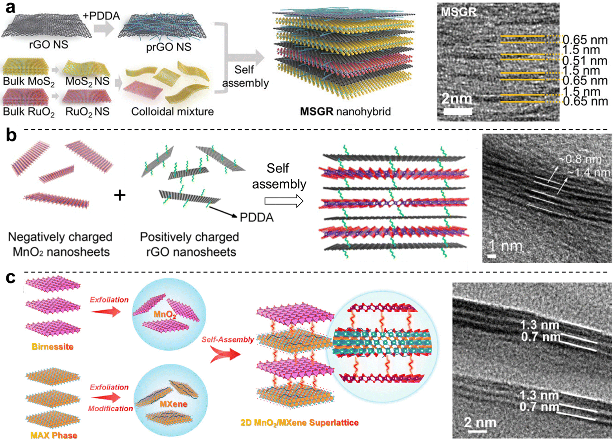 | ||
| Fig. 7 Exfoliation/restacking-based approaches for 2D layered heterostructures. (a) Assembly of PDDA-modified rGO with RuO2 and MoS2 leading to ordered 2D heterostructures; (b) assembly of oppositely charged MnO2 and PDDA-modified rGO; and (c) assembly of MnO2 with PDDA-modified Ti3C2Tx MXene. Panel (a) is adapted with permission from John Wiley & Sons, Inc.151 Panel (b) is adapted with permission from The American Chemical Society.152 Panel (c) is adapted with permission from The American Chemical Society.153 | ||
Electrostatic-induced assembly between oppositely charged nanosheets can also be exploited directly in a colloidal dispersion. Ma and co-workers reported the formation of 2D layered heterostructures via the dropwise addition of a dispersion of anionic TiO nanosheets to a dispersion of cationic GdEu nanosheets in a formamide dispersion under continuous stirring at a concentration ratio which would provide surface area matching.154 The flocculated product resulting from this was washed several times prior to sonication to form a homogenous suspension, and free-standing membranes were then fabricated via simple vacuum filtration. The authors of this study noted the importance of choosing the sonication time which is long enough to achieve a well-dispersed suspension, whereas excessively long sonication times could damage the nanosheets and their heterostructures. Despite the “bulk” filtration approach to heterostructure formation, TEM showed that the GdEu/TiO heterostructures consisted of alternating layers with interlayer spacings on the order of 0.85 nm and 0.75 nm, corresponding to GdEu and TiO, respectively.
More recently, emerging 2D materials such as MXenes and BP have also been used in colloidal approaches for the formation of 2D nanomaterial heterostructures, followed by their deposition via vacuum filtration to form free-standing membranes. Well-dispersed aqueous dispersions of MXene with rGO were mixed at the desired ratios prior to vacuum filtration to achieve MXene-rGO free-standing membranes, where the presence of MXene sheets drastically improved the degree of alignment of the rGO sheets, greatly improving both the electrical conductivity and mechanical properties of the heterostructure compared to the constituent 2D nanosheets.155,156 Similarly, MXene modified with PDDA also provided a well-defined 2D heterostructure superlattice with high stability and facilitated fast charging/discharging ion diffusion for energy storage (Fig. 7c).153 A similar approach was also used for the fabrication of rGO-BP films, which exhibited a record mechanical toughness of ∼52 MJ m−3.157 Furthermore, the electrostatic assembly of ZnIn2S4 with MoSe2 to form 2D heterostructures has shown that this approach can also yield layered composites with drastic improvements in their functional properties, particularly in photocatalytic H2 evolution.158
In summary, layered nanomaterials obtained by LPE can be assembled into well-ordered layered heterostructures, following the approaches described above. However, the negative effects of LPE on the obtained 2D materials, namely, high layer number and edge-length polydispersity and the formation of surface defects, make it challenging to control and define the photophysical and interfacial properties of the heterostructure. Furthermore, these types of systems are well-suited for the fabrication of films, but generally unusable in colloidal applications such as aqueous-phase photocatalysis. In an effort to overcome these shortcomings, colloidal synthetic methods to make well-defined layered heterostructures offer suggestions for future advances in this area.
5. Colloidal modification of 2D material interfaces – toward surface-chemistry-controlled heterostructure synthesis
5.1. 2D Janus nanosheets
The principles of LbL and electrostatic assembly can also be applied when using a spherical “core” with interaction characteristics that favor the attachment of the first layer of 2D materials, whereas this first layer serves as an anchor for the following layers of other 2D materials necessary to form a heterostructure. De Gennes first described the characteristics of particles with two different components on the same surface in terms of the Roman god “Janus” in his Nobel lecture in 1991.159 In the 3 decades since then, the development of “Janus” materials, or materials/particles with two distinct regions of different surface chemistry, composition, or properties has experienced significant progress. The first particle termed “Janus” was achieved in 1989 by embedding glass particles in a planar matrix, while the exposed regions of the particles were treated with octadecyltrichlorosilane to achieve a hydrophobic, organically modified region and a hydrophilic glass region.160 Due to their amphiphilicity, they could be used to stabilize emulsions via their assembly at oil/water interfaces.Along these lines, the stabilization of emulsions with solid particles was discovered by Ramsden and Pickering, which led to the establishment of these systems as “Pickering Emulsions”.161,162 In addition to Pickering emulsions, classic emulsion polymerization processes carried out on seed particles can provide a scalable means to produce asymmetric particles by controlling phase separation and the thermodynamics and kinetics of polymerization in these systems. In the context of 2D nanomaterial heterostructures, the field of 2D Janus nanosheets provides numerous interesting examples of how 2D crystals with defined surface chemistry on either side of the basal surface can be achieved. In general, the strategies involved are based on either partial protection and modification, as in the example given at the end of the previous paragraph, or the controlled phase separation of multiple components. However, phase separation-based strategies tend to be confined to purely organic systems rather than modified 2D materials, and thus readers interested in these approaches may refer to relevant reviews to learn more about this topic.163
Partial protection strategies for the synthesis of 2D Janus nanosheets have employed a number of different strategies for the modification of the exposed face of the nanosheet, including chemical reactions such as siloxane modification, plasma treatment, sputtering, or exposure to gaseous radical species.164–167 In the latter example, the exposure of chlorine radicals to the unprotected face, followed by the reaction of benzoyl peroxide radicals with the previously protected face provided a fully radical-based synthesis of 2D Janus nanosheets.164 The grafting of radical initiators used in polymer synthesis to 2D materials in a Janus fashion can also be useful for polymerization reactions at the interface, offering the potential for an even greater number of possible chemical modifications. In an example by Leon and co-workers, Pickering emulsions of GO on wax beads were used to modify one side of the GO nanosheets with initiators for atom-transfer radical polymerization (ATRP) on the unprotected face, followed by the grafting of poly(methyl methacrylate) (PMMA) onto these faces by ATRP.168 Furthermore, in this study, the authors also carried out chemical analysis of the two faces of the nanosheets, showing their asymmetric functionalization and providing a firm basis for future studies of 2D Janus nanosheets.
A significant body of work on the synthesis of 2D Janus nanosheets based on inorganic templates or the growth of inorganic solids has been reported in the last decade. In general, this involves the use of a hollow inorganic shell (such as one formed by a Pickering emulsion), followed by modification of the exposed or outer part of the shell via various approaches, such as polymer growth, molecular adsorption, inorganic material synthesis, etc. Finally, when a sheet-like structure is desired, the modified hollow particle is then thoroughly crushed, providing the Janus 2D nanosheets which can be further chemically modified at either interface to gain greater control over surface chemistry (Fig. 8).169–173 The use of Janus nanosheets to drive inorganic synthesis at the interface is one approach through which 2D nanomaterial heterostructures can be achieved. For example, Yang and co-workers used Janus nanosheets prepared via a Pickering-emulsion-based approach to drive the selective growth of Fe3O4 nanoparticles on the hydrophilic side of the Janus sheet, which was facilitated by Fe ions complexing with free carboxylic acid groups present on the surface.174 Similarly, the large disparity in surface chemistry and chemical environment between the two interfaces has been shown to permit the selective growth of Au,174 TiO2,175 Ag,176 and other metals on one of the two interfaces of Janus nanosheets. These examples reinforce the concept that control over surface chemistry can provide the means to restrict the growth of materials at specific interfaces, which will come into play in future strategies for achieving better control over the direct colloidal synthesis of 2D nanomaterial heterostructures.
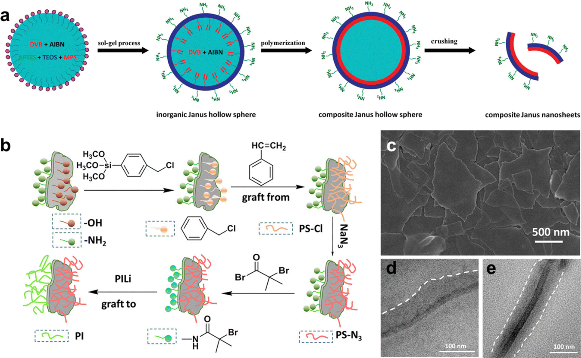 | ||
| Fig. 8 2D Janus nanosheets: (a) synthesis of silica-polymer 2D Janus nanosheets; (b) synthesis of silica-based 2D Janus nanosheets with polyisoprene on one side and azide-terminated polystyrene on the other side; (c) SEM image of 2D Janus silica nanosheets; TEM images of 2D Janus nanosheets with (d) one side functionalized with polystyrene, and (e) one side modified with polystyrene and the other with polyisoprene. Panel (a) is adapted with permission from The American Chemical Society.177 Panels (b)–(e) are adapted with permission from The American Chemical Society.178 | ||
While approaches similar to those described in the above paragraph can yield a wide range of Janus 2D nanosheets, major drawbacks remain which hinder the development of well-defined colloidal 2D nanomaterial heterostructures. First, the need for crushing the hollow shell to recover the 2D Janus nanosheets from the modified shell “template” leads to a very broad size dispersity of the resulting sheets, which severely limits the use of this method for producing well-defined colloidal dispersions based on these particles. Second, this also means that the shape dispersity of the resulting particles is poor, where irregularly shaped flakes with a broad range of edge-lengths tend to be formed. Furthermore, the use of a curved template particle can lead to bent or pitched nanosheets, and this has a particularly strong impact on Janus nanosheets where the growth of an inorganic material atop the spherical template is carried out. The formation of ordered 2D heterostructures from such nanosheets would be greatly hindered due to these drawbacks.
5.2. “Pillaring” of 2D materials – a route to control chemistry in confined spaces
The various methods described above show that broad segments of the scientific community are interested in the synthesis of well-defined 2D layered heterostructures. In particular, many of the recent advances have been based on colloidal approaches, due the inherent advantages of colloidal methods compared to traditional methods. Despite the capability of vapor-phase approaches to achieve epitaxial growth and well-defined growth of layers with controllable registry between 2D material layers, they are expensive, time-consuming, resource-intensive, and cannot be easily transferred to liquids as colloids. On the other hand, colloidal techniques such as LbL assembly, exfoliation/restacking, and Janus particle-based approaches all suffer from different limitations which cannot be easily counteracted. In particular, these techniques generally involve LPE of the 2D materials to a colloidal dispersion prior to their use. For these reasons, it is clear that the direct colloidal growth of 2D nanomaterial heterostructures can be advantageous to LbL, exfoliation/restacking, and other methods which rely on LPE as a starting point. Direct growth of 2D materials templated at the interface of nanosheets in colloidal dispersion requires careful control of the surface chemistry of the nanosheets, so that the growth of the 2D material is limited to the desired surface. Important lessons regarding the templated growth of nanomaterials can be found in earlier studies of growth in clay-like materials. In particular, swelling clays of the smectite family such as montmorillonite, saponite, LAPONITE®, etc. have been studied early on in the context of the formation of inorganic pillared clays.Since the concept of pillared clays was first developed by Barrer and MacLeod in 1955,179 in which the exchange of interlayer cations in montmorillonite with alkylammonium was used to induce interlayer porosity, many researchers have reported the “pillaring”, or the formation of ordered vertical stacks of layered clays, with surfactants or other organic molecules.180,181 In general, organocations based on the ammonium moiety have been widely used (II, Fig. 9).182 The use of inorganic ions to induce pillaring of the clays was also shown (III, Fig. 9), where the subsequent condensation of the inorganic ions to form solids within the interlayer serve as early examples of 2D inorganic heterostructures, generally for applications in catalysis.183–185 The first examples of these include the condensation of Al ions in 1977 by Brindley and Sempels,186 and the hydrolysis of silicon acetylacetonate and tantalum or niobium metal clusters by Pinnavaia et al. in 1984 (IV, Fig. 9).187 Numerous studies have been carried out in which metal oxides such as ZrO2,188–192 TiO2,193–195 CrxOx,196–199 and Al2O3200–202 were grown in the interlayer space of clay-like materials, layered silicates in particular, which then led to the growth of Y-zeolites in the interlayer, resulting in porous materials effective for catalysis.183
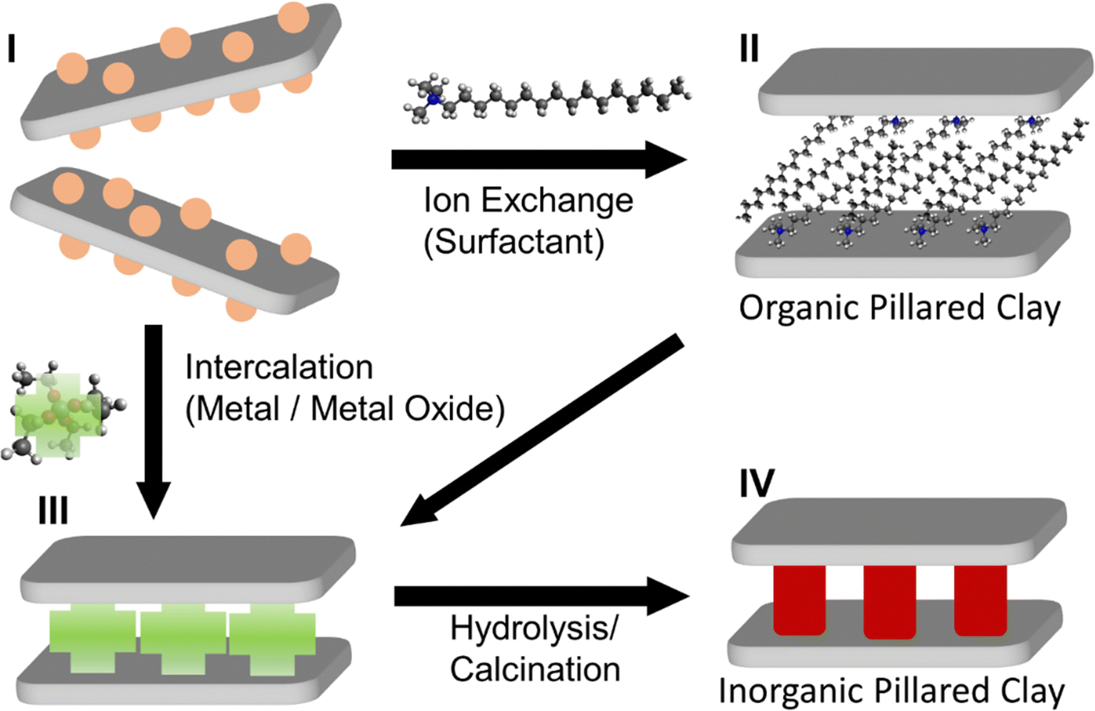 | ||
| Fig. 9 Schematic of the modification of layered clay-like materials to achieve organic or inorganic pillared clays. (I) A layered material with basal surface charges compensated by counterions (shown in orange); (II) exchange of counterions with charged surfactants (CTAB is shown) as organic ions provides an organic pillared clay; (III) the intercalation with metal oxide species (from II, tetraethylorthosilicate (TEOS) shown) or exchange of metal ions (from I) provides a metal or metal-oxide intercalated layered material; and (IV) calcination or hydrolysis (in the case of TEOS and comparable metal oxides) leads to the formation of inorganic metal oxide “pillars” in the interlayer space between clay-like sheets. | ||
More recently, both inorganic and organic pillaring strategies have been developed for the modification of emerging 2D materials to improve their functionality. TMDs such as MoS2, with weak interlayer bonding, allow for the intercalation of various molecules, both charged and uncharged.203–206 Amines serve as generally useful pillaring agents as they can be protonated to a cationic state in an aqueous environment, and many studies have reported the use of amines for expanding the interlayer space of TMDs.207,208 Pillaring strategies show great promise for energy storage applications, benefiting from the improvement in battery and supercapacitor function due to improvements in the reversible transport of ions in the interlayer spaces of 2D materials. MXenes in particular have benefited from this, where several studies highlight the use of organic pillaring agents such as tris(2-aminoethyl)amine,209 hydrazine,210 glycine,211 and the common pillaring surfactant cetyltrimethylammonium bromide (CTAB)212,213 to improve the electrochemical storage capacity and cycling stability/lifetime of supercapacitors or batteries based on pillared MXenes. Interestingly, inelastic neutron scattering measurements showed that in the case of pillaring with hydrazine, the fluoride and hydroxyl surface terminations of the MXene basal surface were replaced with hydrazine molecules, whereas glycine was found to lead to the formation of a stable Ti–N bond. In addition to purely organic pillaring strategies, inorganic pillaring strategies involving the formation of silica by calcination, following intercalation/pillaring with an amine, have also been shown to improve the ion storage of MXene-based hybrids for battery applications.214,215 A broad range of other 2D materials have benefitted from pillaring strategies to improve their properties relevant for electrochemical energy storage applications;216,217 however for a more exhaustive list, readers may be interested in recent reviews which focus more specifically on this topic.218,219 Finally, advances achieved through pillaring of 2D materials have also been reported in other fields such as sensing,220 and energy storage;214 however this topic goes beyond of the scope of this review.
6. Direct colloidal synthesis of 2D nanomaterial heterostructures
The lack of well-defined 2D nanomaterial heterostructures formed by direct colloidal synthesis, as opposed to methods where both 2D materials are first synthesized prior to exfoliation/restacking, LbL, or related approaches, highlights the need for renewed efforts in this direction. The above techniques of LbL, Janus nanosheets, and pillaring of 2D materials with organic molecules discussed in Section 5 emphasize the importance of chemical modification of interfaces in achieving predictable growth at interfaces and well-ordered 2D layers. Many 2D-material-based semiconductor heterostructures for photocatalysis largely consists of mixtures of two materials, which generally lack well-defined structures and clear guiding principles for their fabrication approach, making it difficult to transfer the success of these methods to other systems.221–223 There are several reports of photocatalysts based on 2D material heterostructures which have well-defined multi-lamellar structures, but very few of them are fabricated via direct colloidal synthesis. Early work by Ida et al. established Ca2Nb3O10/NiO2 heterostructures prepared using an LbL approach, which resulted in suppressed recombination of photogenerated charges.224 Jiang et al. used an exfoliation/restacking approach to obtain CsPbBr3/BiWO6 2D heterostructures, although the growth of small Pt nanoparticles was necessary to observe improved photocatalytic CO2RR.225 Lin and co-workers reported the fabrication of LDH/Ti3O7 layered heterostructures by exfoliation/restacking, resulting in a superlattice with improved photocatalysis of methylene blue and photocurrent generation.226 A number of other reports of exfoliation/restacking based approaches for the fabrication of 2D material heterostructures exist,227,228 with varying degrees of definition of the lamellar structure; however there are only few examples of direct colloidal synthesis of well-defined 2D material heterostructures thus far. Initial success in the direct colloidal synthesis of 2D nanomaterial heterostructures has been achieved via the stepwise growth of semiconductor chalcogenide nanocrystals in heated mixtures of nanoplates, precursors, and surfactants (6.1) and via surfactant-induced pillaring of charged 2D material templates followed by hydrothermal synthesis (6.2). These methods are described in greater detail below.6.1. Sequential colloidal growth of chalcogenide nanocrystal heterostructures
Semiconductor nanocrystals known as “quantum dots” (QDs) are of significant importance due to their size-dependent optical and electronic properties, and cadmium chalcogenide nanocrystals (CdX, X = S, Se, and Te) in particular have been well-studied regarding their synthesis, surface chemistry, and optical properties.229–233 The synthesis of colloidal nanocrystal QDs is mainly carried out via “hot-injection” and “heat-up” synthesis approaches, in which inorganic precursors and ligands dissolved in organic solvents are heated, leading to the nucleation and growth of colloidally stabilized inorganic nanocrystals.234 In hot-injection, the rapid introduction of a concentrated precursor solution to a hot solution containing surfactants leads to a sudden increase in supersaturation and the formation of nanocrystals, during which surfactant molecules cap the surface of the formed nanocrystals and prevent their agglomeration.113 In heat-up approaches, the reaction mixture is heated slowly to the reaction temperature at which the formation of nanocrystals will take place.235Great control over size and morphology of CdSe nanoparticles has been achieved, allowing for the production of 2D platelets with distinct numbers of atomic layers in thickness.236–240 This is important for the development of optoelectronic applications, as this diminishes spectral broadening of emission and gives rise to fast radiative rates, among other effects.241–244 The interest in enhanced optical properties has led to the development of epitaxial overgrowth of semiconductor layers atop 2D CdX nanoplatelets (NPLs) with a smaller bandgap, leading to quantum confinement-related increases in photoluminescence quantum yield. The control over 2D growth of CdX-based heterostructures has progressed to the point where the thickness can be tuned down to a single layer for both core and shell materials, with a broad range of possible photoluminescence wavelengths from the near-ultraviolet to the near-infrared.241,242,245–248 The typical structures that can be formed in this manner are known as either “core/crown” for 2D growths atop a sheet, or “core/shell”, in which the core is completely enclosed. In 2012, Dubertret and co-workers reported a room-temperature approach to limit the growth of CdS or CdZnS layers on CdSe via a ligand-exchange route.249 In their approach, thiolate ligands were used to substitute carboxylate ligands on the CdSe NPLs, providing a sulfide layer and simultaneously blocking further growth. Further control over subsequent growth steps is achieved by coating NPLs with a bis-trimethylsilylated sulfur compound (TMS2S), which is capable of selectively reacting with and displacing carboxylate ligands to achieve a TMS-S bound to a Cd atom at the NPL surface.250,251 The NPL solution is then washed to remove excess TMS2S, breaking remaining TMS-S bonds and producing sulfide-rich surfaces, which, in the next step, react with cadmium ions added to the dispersion to achieve the growth of a CdS layer atop the CdSe NPL (Fig. 10a and b).
 | ||
| Fig. 10 (a) Scheme of the layer-by-layer CdS shell growth on a CdSe NPL. (b) HAADF-STEM image of a CdSe/CdS core/shell NPL. (c) Photographs showing the sequential growth of a CdS shell on CdSe NPLs via c-ALD. The addition of K2S transfers the NPLs from toluene to formamide. NPLs are then transferred back to toluene via the addition of didodecyldimethylammonium bromide (DDAB). The excess of DDAB is removed via extraction with formamide, and the Cd layer is then grown on the surface terminated with S2−. (d) High- resolution TEM image of the edge of a CdSe/CdS NPL after seven c-ALD cycles. Panels (a) and (b) are adapted with permission from The American Chemical Society.249 Panels (c) and (d) are adapted with permission from The American Chemical Society.252 | ||
A variation of these methods that has shown strong control over the growth of 2D heterostructures is known as colloidal ALD (c-ALD), a method which was first described by Talapin and co-workers in 2012 for the growth of CdS shells on CdSe nanocrystals.252 c-ALD is a process in which the removal of ligands, addition of cadmium and chalcogenide ions, and reattachment of ligands to a nanocrystal surface are iterated to achieve precise control over the growth of the shell. This approach allows facile tailoring of the resulting surface chemistry, as the final step is the reattachment of ligands, and NMR studies have shown that roughening and increased chemical disorder at the surface occur during the process of ligand removal and shell growth.253 In c-ALD, the sequential solvent extraction of nanocrystals and precursors between synthetic steps prevents the accumulation of excess precursors and synthetic by-products, reducing non-uniform growth and allowing more facile stoichiometric control. In order to produce 2D heterostructures, the growth step is carried out in a polar phase following the approach from the seminal report on this method (Fig. 10c and d). In the first step, N-methylformamide (NMF), hexane, (NH4)2S, and CdSe nanoplatelets (NPLs) dissolved in hexane are stirred until complete phase transfer of NPLs to NMF. In step 2, the polar phase is rinsed with hexane to remove excess ligands, and then the NPLs are precipitated with acetonitrile and redispersed in fresh NMF. In step 3, the Cd precursor in NMF is added to the clean NPL dispersion in NMF, and the mixture is stirred briefly (30–60 s). Finally, the NPLs are precipitated with an organic solvent such as toluene and redispersed in clean NMF. Overall this process require around 10 min or less per CdS layer grown, with minimal losses of NPLs during each step. The step-wise nature of c-ALD also permits tailoring not only the number of individual atomic layers deposited, but also the composition of each semiconductor layer that is deposited. For example, Talapin and co-workers demonstrated layered heterostructures of multiple alternating materials, such as CdS, ZnS, and CdSe (Fig. 11a).240
 | ||
| Fig. 11 (a) HAADF-STEM image of 2CdS/2ZnS/2CdS/4CdSe/2CdS/2ZnS/2CdS formed by c-ALD using Li2S/Li2Se and anhydrous Cd(HCOO)2/Zn(OAc)2 powders as the sources of chalcogen and metal precursors, respectively; (b) the interplanar distances for this structure shown in (a); (c) schematic representation of the cation exchange of CdSe/CdS core/shell NPLs to ZnSe/ZnS and PbSe/PbS NPLs with corresponding HAADF-STEM images. Panels (a) and (b) are adapted with permission from The American Chemical Society.240 Panel (c) is adapted with permission from The American Chemical Society.254 | ||
In an effort to extend the range of possible semiconductors achieved by sequential deposition of nanocrystal layers, cation exchange reactions were examined, as they provide a means to obtain nanocrystals with compositions and/or morphologies which can be difficult to obtain via direct synthetic means.250,251 Previous work, primarily carried out by the Alivisatos and Manna groups, had shown that sequential cation exchange processes using copper chalcogenides as intermediates provided a route to change the composition of various shapes without impacting the nanocrystal morphology.255–260 Studies by Jeong and co-workers in 2011 reported the cation exchange of TiS2 nanodiscs with Cu ions to achieve a heteroepitaxial TiS2–Cu2S structure, although in their case the nanodisc morphology was altered, resulting in a toroidal morphology.261 The Dubertret group carried out a series of sequential cation exchange processes in order to achieve Cu2Se/Cu2S, ZnSe/ZnS and PbSe/PbS 2D heterostructures254 (Fig. 11c): First, CdSe/CdS NPLs were obtained according to the c-ALD method of Ithurria and Talapin.252 Next, the CdSe/CdS NPLs were mixed with a copper(I) complex at an excess of 5–10 times the amount of Cd, leading to an immediate change in color indicating successful cation exchange. Third, following washing and resuspension of the Cu-exchanged NPLs, cation exchange of Cu with Pb and Zn is carried out. In the case of Pb, the exchange is carried out at room temperature with an excess of Pb,262 and in the case of Zn, a hot-injection approach is employed in the presence of excess Zn.263
While sequential surface modification and growth approaches discussed in this section such as c-ALD show a powerful ability to achieve tailorable layer number and composition, with a high degree of shape and size monodispersity, there are inherent limitations to these approaches. First of all, these approaches are limited to chalcogenides, specifically cadmium chalcogenides, which have been the focus of the majority of research in this direction. In particular, CdS/CdSe has become one of the most well-studied systems regarding the controlled growth of 2D nanomaterial heterostructures. As discussed above, cation-exchange approaches can be used to broaden the potential options for semiconductor hybrids; however, these are still limited in scope, as CdSe/CdS NPLs are still used as starting materials for the cation exchange process. Furthermore, cation exchange processes can only be used for certain elements as chalcogenides (e.g., Cu, In, Pb, and Zn), and the necessity for copper chalcogenides as intermediates further limits the possible materials that can be achieved via these approaches. Recent work by the Buonsanti group has shown that c-ALD is also a useful approach for growing ultrathin oxide layers at the interface of a variety of colloidal nanocrystals,264,265 which shows that the range of materials achievable through this approach continues to grow; however, such approaches have not yet been widely applied to NPLs to achieve 2D heterostructures. Finally, a major drawback of c-ALD is the need for carboxylate ligands, which are the key element in the stepwise growth which enable the synthesis of such core–shell type structures.265 This reduces the generalizability of the method, and limits its scope to materials which can be effectively passivated with carboxylate ligands.
While the sequential approaches such as c-ALD show the greatest degree of control over shell growth, they are hindered by the time-consuming nature of the sequential process, in addition to the potential waste of precursors and undesirable nucleation at the NPL interface if the cleaning process is not completely successful. As such, direct shell growth via hot-injection has been sought. Authors have reported ZnS shell growth on CdSe NPLs to achieve a quantum yield of >50% at moderate temperatures of 100–150 °C,246 and ZnS/CdSe NPLs with quantum yields close to unity could be synthesized by hot-injection at 300 °C.266 However, the majority of such one-pot hot-injection approaches lack control over layer number and composition compared to sequential methods, and one must consider the benefits and disadvantages of the two approaches based on the target application or study.
6.2. Hydrothermal synthesis in “Pillared” layered materials
The direct synthesis of heterostructured nanomaterials via colloidal routes (most commonly based on hydrothermal or solvothermal methods) has been a topic of intense interest in the last few decades, largely driven by the development of heterostructured photocatalysts. The bands of semiconductors in a heterostructure can be aligned in order to achieve a variety of photocatalytic reactions, such as hydrogen evolution reaction (HER), oxygen evolution reaction (OER), oxygen reduction reaction (ORR), and CO2 reduction reaction (CO2RR). These alignment strategies are commonly referred to as “type II” heterojunctions with a staggered band alignment between semiconductors,267 and they include the “Z-scheme” for coupling of photocatalysts through a shuttle redox ion mediator,268,269 and the “S-scheme” involving a heterojunction of reduction and oxidation photocatalysts with a staggered band structure.270,271 Of particular interest to the community in recent years is the development of new photocatalysts for water splitting, which combine both HER and OER to result in the splitting of water into H2 and O2 using light, a reaction of great significance for the energy transition towards using hydrogen fuel cells as a means of power and propulsion in future generations. While efforts to synthesize novel photocatalysts from semiconductor heterostructures have been successful, few example, well-defined 2D heterostructures grown colloidally have been reported. On the other hand, many of the successful examples include the growth of small amounts of nanoparticles (typically catalytically active metals such as Pt and Pd) atop semiconductors, or in the presence of two semiconductors aggregated or mixed together.272,273 While the use of catalytic metals is especially needed for the OER side of the water splitting process, “metal free” semiconductor heterostructures are highly sought after due to their reduced costs. However, the majority of reported semiconductor heterostructures based on 2D materials consist of small spherical nanoparticles of one semiconductor grown atop a 2D material.274–276 Otherwise, when direct growth of 2D materials together is performed, the structural organization of these heterostructures is usually poorly defined.276–280As discussed in Section 5.2, the modification of charged 2D materials with surfactants via ion-exchange can lead to the “pillaring” of the 2D materials, whereby the modification of the basal surface leads to quasi-ordered vertical stacking. Recent efforts have highlighted the potential of organic pillaring for modifying the chemical environment of the basal surfaces and interlayer spaces of 2D materials in order to aid synthesis in this confined space.281–284 In particular, clay-like materials such as layered silicates,281,282,284 LDHs,283 and MXenes,285 which are easily modified with oppositely charged surfactants, can serve as templates for the growth of 2D materials by virtue of the altered chemical environment at the interface where surfactant modification occurs. In general, modifications of the basal surfaces (when fully exfoliated) or interlayer spaces (where pillaring has occurred), which provide an energetically favorable environment for precursor ions and molecules to reside, can provide a driving force for the formation of well-defined layered heterostructures through a single synthetic method. Early research in this direction made use of the layered silicate LAPONITE®, which has a thickness of 1 nm and a diameter of 25 nm, a high cation exchange capacity (CEC), well-described phases, and a useful template for testing such pillaring approaches.286–293
Earlier studies of LAPONITE® showed that it could serve as a shape template for the growth of gold nanoparticles aided by the reduction of Au(III) to Au(I) at the LAPONITE® surface, where disc-shaped gold nanoparticles were obtained.294 This paved the way for studies of noble metal nanoparticle growth in layered nacre-like materials.295 The templated growth of Au on LAPONITE® led to the idea that a favorable chemical environment for the adsorption of 2D material precursors at interfaces could provide the means to achieve the colloidal growth of 2D nanomaterial heterostructures. Along these lines, the surfactant CTAB induces the pillaring of layered silicates into quasi-ordered stacks while also conferring hydrophobic character to the modified interlayer space. In the first effort to arrive at a 2D nanomaterial heterostructure based on TMDs, MoS2 was grown in the CTAB-modified interlayer space of LAPONITE® (Fig. 12a).281 The smallest observed particles resulting from this synthesis exhibited the typical discoidal morphology of LAPONITE®, with an edge length of around 25 nm and somewhat irregular edge shape (Fig. 12b). However, in contrast to LAPONITE®, which is hardly visible via TEM due to the low atomic number of Mg and Si, the particles were clearly visible, and the lattice fringes of MoS2 were clearly observed (Fig. 12d). Not only did EDX measurements support the colocalization of elements from both LAPONITE® and MoS2, but electron diffraction also revealed hexagonal crystalline symmetry typical of MoS2, showing that the MoS2 layers were grown in plane with the discoidal template (Fig. 12c). As it is possible for such 2D layered heterostructures to be terminated by either of the two constituent 2D materials, it was determined by zeta potential measurements and dye aggregation experiments (methylene blue adsorption)296 that LAPONITE® constituted the terminal layers of the heterostructure. This provided significantly improved dispersibility and catalytic activity in aqueous media compared to MoS2 (Fig. 12e and f). Furthermore, photoluminescence (PL) measurements have also revealed that these LAPONITE®–MoS2 heterostructures are composed of single layer MoS2, as the PL is drastically increased and indicative of the formation of a direct bandgap based on previous reports of monolayer MoS2.297
 | ||
| Fig. 12 (a) Scheme of the colloidal synthesis of LAPONITE®–MoS2 layered heterostructure nanoparticles; (b) TEM micrographs of irregular discoidal morphology resembling LAPONITE®; (c) electron diffraction showing the single-crystalline nature of grown MoS2 with typical hexagonal symmetry; and (d) high-resolution TEM showing the typical lattice planes for MoS2. (e) Catalysis of methyl orange degradation by BH3− influenced by 0.04 mg mL−1 MoS2 and LAPONITE®–MoS2 and (f) dispersion of MoS2 and LAPONITE®-MoS2 directly after dispersion (0 h) and after 48 h of settling. Adapted with permission from the American Chemical Society.281 | ||
As reducing the thickness of non-layered semiconductors can improve their optical and photocatalytic properties due to reduced photoinduced charge-carrier recombination, the pillaring-based approach was extended to synthesize other semiconductors in the confined interlayer space. The semiconductor β-In2S3 was successfully grown via a similar approach, which resulted in the growth of In2S3 lamellae ∼1 nm thick between layered silicate sheets (Fig. 13a and c).282 This drastically altered the optical properties of In2S3, actually reducing the absorption of light in the visible region. However, the photocatalytic degradation of methyl orange and photocurrent produced under visible light were increased by more than an order of magnitude compared to In2S3, which was attributed to the improved charge separation/reduced recombination of photoinduced charge carriers. This was followed by the study of ZnIn2S4, which has a similar crystal structure as In2S3, but can exhibit superior photocatalytic activity under visible light irradiation. Interestingly, in the case of ZnIn2S4, the leaching of Mg from the octahedral layer of LAPONITE® led to the formation of Zn defects in ZnIn2S4, which in turn led to drastically improved photocatalytic properties compared to ZnIn2S4 (Fig. 13b).284
 | ||
| Fig. 13 (a) Scheme of the colloidal synthesis of LAPONITE®–In2S3 layered heterostructures; (b) TEM micrographs of LAPONITE®–ZnIn2S4; the zoomed inset shows layer thickness and lattice spacings of ZnIn2S4 lamellae; (c) TEM micrographs of LAPONITE®–In2S3; the zoomed inset shows lattice spacings of In2S3 lamellae; schematic of the LAPONITE®–In2S3 layered heterostructure, and photographs and quantum efficiency of photocatalysis of In2S3 compared with LAPONITE®–In2S3. Panels (a) and (c) are adapted with permission from the American Chemical Society.282 Panel (b) is adapted with permission from the American Chemical Society.284 | ||
The growth of other visible-light photocatalysts with intrinsically stacked crystalline structures was also attempted, in an effort to find the limitations of this approach. In this regard, the growth of Bi2MoO6, with an Aurivillius perovskite-type structure composed of alternating (Bi2O2)2+ and (MoO4)2− layers, was templated using a similar approach.298 However, in contrast to the examples given in the prior paragraph, the formation of a heterostructure was accompanied by the formation of micron-size single-crystalline particles composed of both LAPONITE® and Bi2MoO6. It was determined that under low pH conditions during synthetic, the protonated LAPONITE® Si–OH edge sites were bridged by the dianionic (MoO4)2− species, resulting in an extended structure where nucleation and growth then occurred. In comparison, the templated growth of Bi2MoO6 using sodium dodecyl sulfate (SDS)-modified CoAl LDH led to the formation of a well-defined Bi2MoO6/LDH heterostructure.283 Interestingly, in both of the above Bi2MoO6-based heterostructures, the confinement of synthesis at a 2D template interface exerted a considerable influence on the preferred crystalline growth orientation, which is also referred to as “facet engineering”, and is important for the development of semiconductor photocatalysts.299,300 The improved adsorption and retained photocatalytic activity of Bi2MoO6 made these hybrids highly effective as photocatalytic sorbents in anti-fouling water decontamination membranes.301 In some cases, it was also possible to achieve templated growth by controlling surface chemistry at the interface without pillaring. For example, LAPONITE® modified with PVP and d-mannitol was able to template the growth of the visible-light photocatalyst bismuth oxyiodide, BiOI.302 Bismuth oxyhalides are gaining interest as photocatalytic materials, due to their intrinsic internal electric field (IEF) which can improve charge separation and thereby reduce the recombination of photo-generated electrons and holes.303–305 This templated growth led to facet engineering, where dominant {100} surface facets orthogonal to the direction of the IEF enhanced photocatalytic properties, while the confined BiOI growth drastically altered the optical properties.
Overall, the synthesis of 2D nanomaterial heterostructures via surfactant modification and pillaring of 2D nanomaterial templates followed by hydrothermal or solvothermal synthesis offers a promising single-step approach which has been proven for the growth of a number of semiconductors. However, this technique suffers from some specific limitations. First of all, the modification of the 2D material template with surfactants is generally controlled by ion-exchange, and thus the method is currently limited to 2D nanomaterials with charged basal surfaces. Even so, there are a wide variety of potential 2D materials with functional properties suitable for various applications, and thus far, our group has shown that layered silicates, layered double hydroxides, and MXenes are suitable ionic templates for this approach. Furthermore, the approach also works for directing growth within 1D templates, as the growth of In2S3 has been carried out inside surfactant-modified Ge-imogolite nanotubes.306 (ref erwan) The second main drawback is the lack of understanding about the fate of the surfactant used for pillaring. The presence of organic matter in between semiconductor layers cannot be easily controlled as in the case of c-ALD, and this may lead to altered properties and reduced coupling between layers, which could negatively impact charge transfer processes at the interface. Finally, a third potential drawback of this approach is the possibility of template degradation or side-reactions induced by the high temperature and pressure of hydrothermal processes. We and others have shown that hydrothermal conditions can lead to the formation of TiO2 at the interface of MXenes. It has been also discussed above how Mg2+ leaching from LAPONITE® during hydrothermal synthesis of ZnIn2S4 could lead to the formation of Zn defects.(ref) This could also potentially be a benefit, as it could provide strategies to control doping or defect formation in the grown or template materials.
7. Outlook and perspectives
The advent of 2D materials and their interesting and useful optical and electronic properties has paved the way for future advances in materials science and applications (Section 1). In particular, the use of 2D materials to form layered heterostructures can give rise to new properties and effects. In this review, the main approaches to fabricate 2D nanomaterial heterostructures were covered, as summarized in the scheme below (Fig. 14). The field of research in this direction has largely depended on non-colloidal methods for the fabrication of well-defined 2D material heterostructures (Section 2). The most commonly employed colloidal approaches thus far have been LbL and exfoliation/restacking techniques (Section 4), which can present an array of problems due to the damage, defect formation, and other challenges presented by liquid-phase exfoliation necessary to obtain the 2D materials used in these approaches (Section 3). Colloidal synthetic methods for achieving 2D nanomaterial heterostructures, on the other hand, remain underexplored due to the challenge of achieving well-defined nanostructures under the synthetic conditions necessary for the growth of many target materials. Furthermore, there is a need for a deeper understanding of the relationship between surface chemistry of 2D materials and synthetic outcomes, which is critical for successful colloidal synthetic approaches. | ||
| Fig. 14 Summary of state-of-the-art approaches for the synthesis of 2D nanomaterial heterostructures. | ||
Colloidal approaches come with their own set of challenges which make it difficult to achieve well-defined 2D–2D heterostructures, due to a number of reasons. First of all, ligand or surfactant-induced surface interactions can influence the stacking order and interlayer separation, complicating the achievement of emergent electronic and magnetic properties which can be achieved through vapor-phase and mechanical transfer approaches. Incompatible crystalline lattices, a complete lack of epitaxy, and the presence of ions and ligands further complicates this issue. Another major challenge is optimizing the synthetic conditions so that materials do not grow apart from template, and that growth within/atop the template 2D material is uniform. Finally, there is the challenge of characterization, where TEM imaging at the correct angle is needed to clearly observe the two layers, which can be further complicated by the presence of significant organics, or when using 2D materials containing elements with a low number of electrons that cannot be resolved.
How can we improve the next generation of colloidal 2D layered heterostructures? There are numerous examples from intersecting fields discussed, which can serve as a guide for future efforts in the direct colloidal synthesis of 2D nanomaterial heterostructures. Crucially, careful control over interfacial reactions is necessary to prevent uncontrolled growth beyond the desired interface (Section 5). Janus nanosheets with defined chemistry for selective interactions with precursors is one approach that may address this challenge, while the main drawback of this approach is the lack of control over size/morphology of the Janus nanosheets themselves. 2D Janus nanosheets derived from Pickering emulsion-based surface modification techniques provide an approach to achieve a vast variety of different surface chemistries, which can be used to further guide colloidal growth on one or the other side of the two faces of these materials (Section 5.1). The use of 2D material templates with well-defined face vs. edge surface chemistry can also allow greater control over synthesis at such interfaces.307–315 Surfactant pillaring, where the formation of ordered stacks of 2D materials occurs through surfactant intercalation, can provide a favorable environment in the interlayer space for the precursors of different inorganics (Section 5.2). Our group has utilized this approach in particular to realize a family of colloidally synthesized layered 2D heterostructures (Section 6.2), showing the potential of this method. The state of the art of colloidal synthesis of 2D material heterostructures also encompasses the sequential growth of atomic layers in semiconductor chalcogenide nanoplates, as discussed in Section 6.1. As discussed, the majority of literature reports concerning the direct synthesis of 2D nanomaterial heterostructures beyond these topics feature uncontrolled growth and mixing of 2D materials as the chief approaches. Researchers should make an active effort to improve the size and shape dispersity of their heterostructures, as this will lead to more well-defined properties and greater utility for self-assembly-based approaches. Careful control of surface chemistry at interfaces, interactions between colloidal particles, and the tendency of molecular precursors to react at specific interfaces of 2D materials will prove to be increasingly important as well-defined 2D material heterostructures are sought. Such improvements in this field will enable advances in a plethora of applications, particularly aqueous-phase (photo)catalysis,316–318 sensing,319 optoelectronics,70 and energy storage.320,321
Conflicts of interest
There are no conflicts to declare.Acknowledgements
E. H. H. is supported by the Cluster of Excellence “Advanced Imaging of Matter” of the Deutsche Forschungsgemeinschaft (DFG)—EXC 2056—project ID 390715994.References
- K. S. Novoselov, D. Jiang, F. Schedin, T. J. Booth, V. V. Khotkevich, S. V. Morozov and A. K. Geim, Two-Dimensional Atomic Crystals, Proc. Natl. Acad. Sci. U. S. A., 2005, 102(30), 10451–10453, DOI:10.1073/pnas.0502848102.
- S. Z. Butler, S. M. Hollen, L. Cao, Y. Cui, J. A. Gupta, H. R. Gutiérrez, T. F. Heinz, S. S. Hong, J. Huang, A. F. Ismach, E. Johnston-Halperin, M. Kuno, V. V. Plashnitsa, R. D. Robinson, R. S. Ruoff, S. Salahuddin, J. Shan, L. Shi, M. G. Spencer, M. Terrones, W. Windl and J. E. Goldberger, Progress, Challenges, and Opportunities in Two-Dimensional Materials beyond Graphene, ACS Nano, 2013, 7(4), 2898–2926, DOI:10.1021/nn400280c.
- J. Di, J. Xia, H. Li and Z. Liu, Freestanding Atomically-Thin Two-Dimensional Materials beyond Graphene Meeting Photocatalysis: Opportunities and Challenges, Nano Energy, 2017, 35, 79–91, DOI:10.1016/j.nanoen.2017.03.030.
- M. Chhowalla, H. S. Shin, G. Eda, L. J. Li, K. P. Loh and H. Zhang, The Chemistry of Two-Dimensional Layered Transition Metal Dichalcogenide Nanosheets, Nat. Chem., 2013, 5(4), 263–275, DOI:10.1038/nchem.1589.
- M. Xu, T. Liang, M. Shi and H. Chen, Graphene-Like Two-Dimensional Materials, Chem. Rev., 2013, 113(5), 3766–3798, DOI:10.1021/cr300263a.
- R. Mas-Ballesté, C. Gómez-Navarro, J. Gómez-Herrero and F. Zamora, 2D Materials: To Graphene and Beyond, Nanoscale, 2011, 3(1), 20–30, 10.1039/c0nr00323a.
- R. Ma and T. Sasaki, Two-Dimensional Oxide and Hydroxide Nanosheets: Controllable High-Quality Exfoliation, Molecular Assembly, and Exploration of Functionality, Acc. Chem. Res., 2015, 48(1), 136–143, DOI:10.1021/ar500311w.
- A. Nakada, M. Higashi, T. Kimura, H. Suzuki, D. Kato, H. Okajima, T. Yamamoto, A. Saeki, H. Kageyama and R. Abe, Band Engineering of Double-Layered Sillén-Aurivillius Perovskite Oxychlorides for Visible-Light-Driven Water Splitting, Chem. Mater., 2019, 31(9), 3419–3429, DOI:10.1021/acs.chemmater.9b00567.
- P. R. Wallace, The Band Theory of Graphite, Phys. Rev., 1947, 71(9), 622–634, DOI:10.1103/PhysRev.71.622.
- G. Ruess and F. Vogt, Hoechstlamellarer Kohlenstoff Aus Graphitoxyhydroxyd, Monatsh. Chem., 1948, 78(3–4), 222–242, DOI:10.1007/bf01141527.
- H. P. P. Boehm, A. Clauss, G. Fischer and U. Hofmann, in Surface properties of extremely thin graphite lamellae, Proceedings of the Fifth Conference on Carbon, Pergamon Press, New York, NY, USA, 1962, vol. 12, pp. 73–80 DOI:10.1016/B978-0-08-009707-7.50013-3.
- H. Shioyama, Cleavage of Graphite to Graphene, J. Mater. Sci. Lett., 2001, 20(6), 499–500, DOI:10.1023/A:1010907928709.
- K. S. Novoselov, et al., Electric Field Effect in Atomically Thin Carbon Films, Science, 2016, 306(5696), 666–669 CrossRef PubMed.
- A. J. Jacobson, Colloidal Dispersions of Compounds with Layer and Chain Structures, Mater. Sci. Forum, 1994, 152–155, 1–12, DOI:10.4028/www.scientific.net/msf.152-153.1.
- M. M. J. Treacy, S. B. Rice, A. J. Jacobson and J. T. Lewandowski, Electron Microscopy Study of Delamination in Dispersions of the Perovskite-Related Layered Phases K[Ca2Nan−3NbnO3n+1]: Evidence for Single-Layer Formation, Chem. Mater., 1990, 2(3), 279–286, DOI:10.1021/cm00009a018.
- R. E. Schaak and T. E. Mallouk, Prying Apart Ruddlesden-Popper Phases: Exfoliation into Sheets and Nanotubes for Assembly of Perovskite Thin Films, Chem. Mater., 2000, 12(11), 3427–3434, DOI:10.1021/cm000495r.
- R. E. Schaak and T. E. Mallouk, Perovskites by Design: A Toolbox of Solid-State Reactions, Chem. Mater., 2002, 1455–1471 CrossRef CAS.
- T. Sasaki, M. Watanabe, H. Hashizume, H. Yamada and H. Nakazawa, Macromolecule-like Aspects for a Colloidal Suspension of an Exfoliated Titanate. Pairwise Association of Nanosheets and Dynamic Reassembling Process Initiated from It, J. Am. Chem. Soc., 1996, 118(35), 8329–8335, DOI:10.1021/ja960073b.
- Y. Omomo, T. Sasaki, L. Wang and M. Watanabe, Redoxable Nanosheet Crystallites of MnO2 Derived via Delamination of a Layered Manganese Oxide, J. Am. Chem. Soc., 2003, 125(12), 3568–3575, DOI:10.1021/ja021364p.
- R. F. Frindt, Single Crystals of MoS2 Several Molecular Layers Thick, J. Appl. Phys., 1966, 37(4), 1928–1929, DOI:10.1063/1.1708627.
- A. D. Yoffe, Layer Compounds, Annu. Rev. Mater. Sci., 1973, 3(1), 147–170, DOI:10.1146/annurev.ms.03.080173.001051.
- J. A. Wilson and A. D. Yoffe, The Transition Metal Dichalcogenides Discussion and Interpretation of the Observed Optical, Electrical and Structural Properties, Adv. Phys., 1969, 18(73), 193–335, DOI:10.1080/00018736900101307.
- A. Splendiani, L. Sun, Y. Zhang, T. Li, J. Kim, C. Y. Chim, G. Galli and F. Wang, Emerging Photoluminescence in Monolayer MoS2, Nano Lett., 2010, 10(4), 1271–1275, DOI:10.1021/nl903868w.
- K. F. Mak, C. Lee, J. Hone, J. Shan and T. F. Heinz, Atomically Thin MoS2: A New Direct-Gap Semiconductor, Phys. Rev. Lett., 2010, 105(13), 2–5, DOI:10.1103/PhysRevLett.105.136805.
- A. Kuc, N. Zibouche and T. Heine, Influence of Quantum Confinement on the Electronic Structure of the Transition Metal Sulfide TS2, Phys. Rev. B: Condens. Matter Mater. Phys., 2011, 83(24), 1–4, DOI:10.1103/PhysRevB.83.245213.
- G. Eda, H. Yamaguchi, D. Voiry, T. Fujita, M. Chen and M. Chhowalla, Photoluminescence from Chemically Exfoliated MoS2, Nano Lett., 2011, 11(12), 5111–5116, DOI:10.1021/nl201874w.
- A. Rycerz, J. Tworzydło and C. W. J. Beenakker, Valley Filter and Valley Valve in Graphene, Nat. Phys., 2007, 3(3), 172–175, DOI:10.1038/nphys547.
- D. Xiao, W. Yao and Q. Niu, Valley-Contrasting Physics in Graphene: Magnetic Moment and Topological Transport, Phys. Rev. Lett., 2007, 99(23), 1–4, DOI:10.1103/PhysRevLett.99.236809.
- Z. Y. Zhu, Y. C. Cheng and U. Schwingenschlögl, Giant Spin-Orbit-Induced Spin Splitting in Two-Dimensional Transition-Metal Dichalcogenide Semiconductors, Phys. Rev. B: Condens. Matter Mater. Phys., 2011, 84(15), 1–5, DOI:10.1103/PhysRevB.84.153402.
- D. Xiao, G. B. Liu, W. Feng, X. Xu and W. Yao, Coupled Spin and Valley Physics in Monolayers of MoS 2 and Other Group-VI Dichalcogenides, Phys. Rev. Lett., 2012, 108(19), 1–5, DOI:10.1103/PhysRevLett.108.196802.
- X. Shen and T. Jun Cui, Planar Plasmonic Metamaterial on a Thin Film with Nearly Zero Thickness, Appl. Phys. Lett., 2013, 102(21), 211909, DOI:10.1063/1.4808350.
- R. A. Maniyara, D. Rodrigo, R. Yu, J. Canet-Ferrer, D. S. Ghosh, R. Yongsunthon, D. E. Baker, A. Rezikyan, F. J. García de Abajo and V. Pruneri, Tunable Plasmons in Ultrathin Metal Films, Nat. Photonics, 2019, 13(5), 328–333, DOI:10.1038/s41566-019-0366-x.
- P. Barquinha, A. Pimentel, A. Marques, L. Pereira, R. Martins and E. Fortunato, Influence of the Semiconductor Thickness on the Electrical Properties of Transparent TFTs Based on Indium Zinc Oxide, J. Non. Cryst. Solids, 2006, 352, 1749–1752, DOI:10.1016/j.jnoncrysol.2006.01.067.
- M. Nakata, H. Tsuji, H. Sato, Y. Nakajima, Y. Fujisaki, T. Takei, T. Yamamoto and H. Fujikake, Influence of Oxide Semiconductor Thickness on Thin-Film Transistor Characteristics, Jpn. J. Appl. Phys., 2013, 52, 03BB04, DOI:10.7567/JJAP.52.03BB04.
- I. D. Barcelos, R. de Oliveira, G. R. Schleder, M. J. S. Matos, R. Longuinhos, J. Ribeiro-Soares, A. P. M. Barboza, M. C. Prado, E. S. Pinto, Y. G. Gobato, H. Chacham, B. R. A. Neves and A. R. Cadore, Phyllosilicates as Earth-Abundant Layered Materials for Electronics and Optoelectronics: Prospects and Challenges in Their Ultrathin Limit, J. Appl. Phys., 2023, 134(9), 090902, DOI:10.1063/5.0161736.
- G. A. Wiegers, Misfit Layer Compounds: Structures and Physical Properties, Prog. Solid State Chem., 1996, 24(1–2), 1–139, DOI:10.1016/0079-6786(95)00007-0.
- J. Rouxel, A. Meerschaut and G. A. Wiegers, Chalcogenide Misfit Layer Compounds, J. Alloys Compd., 1995, 229(1), 144–157, DOI:10.1016/0925-8388(95)01680-5.
- A. V. Powell, Intercalation Compounds of Low-Dimensional Transition Metal Chalcogenides, Annu. Rep. Prog. Chem., Sect. C: Phys. Chem., 1993, 90(7), 177–213, 10.1039/PC9939000177.
- M. Samanta, T. Ghosh, S. Chandra and K. Biswas, Layered Materials with 2D Connectivity for Thermoelectric Energy Conversion, J. Mater. Chem. A, 2020, 8(25), 12226–12261, 10.1039/d0ta00240b.
- B. Frit and J. P. Mercurio, The Crystal Chemistry and Dielectric Properties of the Aurivillius Family of Complex Bismuth Oxides with Perovskite-like Layered Structures, J. Alloys Compd., 1992, 188, 27–35, DOI:10.1016/0925-8388(92)90639-Q.
- S. Liu, W. Miiller, Y. Liu, M. Avdeev and C. D. Ling, Sillen-Aurivillius Intergrowth Phases as Templates for Naturally Layered Multiferroics, Chem. Mater., 2012, 24(20), 3932–3942, DOI:10.1021/cm302342v.
- H. Kunioku, M. Higashi, O. Tomita, M. Yabuuchi, D. Kato, H. Fujito, H. Kageyama and R. Abe, Strong Hybridization between Bi-6s and O-2p Orbitals in Sillén-Aurivillius Perovskite Bi4MO8X (M = Nb, Ta; X = Cl, Br), Visible Light Photocatalysts Enabling Stable Water Oxidation, J. Mater. Chem. A, 2018, 6(7), 3100–3107, 10.1039/c7ta08619a.
- Y. Gogotsi and B. Anasori, The Rise of MXenes, ACS Nano, 2019, 13(8), 8491–8494, DOI:10.1021/acsnano.9b06394.
- A. V. Mohammadi, J. Rosen and Y. Gogotsi, The World of Two-Dimensional Carbides and Nitrides (MXenes), Science, 2021, 372(6547), eabf1581, DOI:10.1126/science.abf1581.
- Y. Gogotsi, M. Alhabeb, L. Clark, B. Anasori, S. Sin, K. Maleski and P. Lelyukh, Guidelines for Synthesis and Processing of Two-Dimensional Titanium Carbide (Ti3 C2Tx MXene), Chem. Mater., 2017, 29(18), 7633–7644, DOI:10.1021/acs.chemmater.7b02847.
- N. C. Frey, J. Wang, G. I. V. Bellido, B. Anasori, Y. Gogotsi and V. B. Shenoy, Prediction of Synthesis of 2D Metal Carbides and Nitrides (MXenes) and Their Precursors with Positive and Unlabeled Machine Learning, ACS Nano, 2019, 13(3), 3031–3041, DOI:10.1021/acsnano.8b08014.
- K. R. G. Lim, M. Shekhirev, B. C. Wyatt, B. Anasori, Y. Gogotsi and Z. W. Seh, Fundamentals of MXene Synthesis, Nat. Synth., 2022, 1(8), 601–614, DOI:10.1038/s44160-022-00104-6.
- E. Lhuillier, S. Pedetti, S. Ithurria, B. Nadal, H. Heuclin and B. Dubertret, Two-Dimensional Colloidal Metal Chalcogenides Semiconductors: Synthesis, Spectroscopy, and Applications, Acc. Chem. Res., 2015, 48(1), 22–30, DOI:10.1021/ar500326c.
- Y. Liu, Y. Huang and X. Duan, van der Waals Integration before and beyond Two-Dimensional Materials, Nature, 2019, 567(7748), 323–333, DOI:10.1038/s41586-019-1013-x.
- P. Kumbhakar, C. Chowde Gowda, P. L. Mahapatra, M. Mukherjee, K. D. Malviya, M. Chaker, A. Chandra, B. Lahiri, P. M. Ajayan, D. Jariwala, A. Singh and C. S. Tiwary, Emerging 2D Metal Oxides and Their Applications, Mater. Today, 2021, 45, 142–168, DOI:10.1016/j.mattod.2020.11.023.
- C. Xu and L. Balents, Topological Superconductivity in Twisted Multilayer Graphene, Phys. Rev. Lett., 2018, 121(8), 87001, DOI:10.1103/PhysRevLett.121.087001.
- J. Liu, Z. Ma, J. Gao and X. Dai, Quantum Valley Hall Effect, Orbital Magnetism, and Anomalous Hall Effect in Twisted Multilayer Graphene Systems, Phys. Rev. X, 2019, 9(3), 31021, DOI:10.1103/PhysRevX.9.031021.
- R. Ribeiro-Palau, C. Zhang, K. Watanabe, T. Taniguchi, J. Hone and C. R. Dean, Twistable Electronics with Dynamically Rotatable Heterostructures, Science, 2018, 361(6403), 690–693, DOI:10.1126/science.aat6981.
- L. Balents, C. R. Dean, D. K. Efetov and A. F. Young, Superconductivity and Strong Correlations in Moiré Flat Bands, Nat. Phys., 2020, 16(7), 725–733, DOI:10.1038/s41567-020-0906-9.
- V. Hung Nguyen and P. Dollfus, Strain-Induced Modulation of Dirac Cones and van Hove Singularities in a Twisted Graphene Bilayer, 2D Mater., 2015, 2(3), 35005, DOI:10.1088/2053-1583/2/3/035005.
- C. Ma, Q. Wang, S. Mills, X. Chen, B. Deng, S. Yuan, C. Li, K. Watanabe, T. Taniguchi, X. Du, F. Zhang and F. Xia, Moiré Band Topology in Twisted Bilayer Graphene, Nano Lett., 2020, 20(8), 6076–6083, DOI:10.1021/acs.nanolett.0c02131.
- H. Yoo, R. Engelke, S. Carr, S. Fang, K. Zhang, P. Cazeaux, S. H. Sung, R. Hovden, A. W. Tsen, T. Taniguchi, K. Watanabe, G. C. Yi, M. Kim, M. Luskin, E. B. Tadmor, E. Kaxiras and P. Kim, Atomic and Electronic Reconstruction at the van der Waals Interface in Twisted Bilayer Graphene, Nat. Mater., 2019, 18(5), 448–453, DOI:10.1038/s41563-019-0346-z.
- A. C. Gadelha, D. A. A. Ohlberg, C. Rabelo, E. G. S. Neto, T. L. Vasconcelos, J. L. Campos, J. S. Lemos, V. Ornelas, D. Miranda, R. Nadas, F. C. Santana, K. Watanabe, T. Taniguchi, B. van Troeye, M. Lamparski, V. Meunier, V. H. Nguyen, D. Paszko, J. C. Charlier, L. C. Campos, L. G. Cançado, G. Medeiros-Ribeiro and A. Jorio, Localization of Lattice Dynamics in Low-Angle Twisted Bilayer Graphene, Nature, 2021, 590(7846), 405–409, DOI:10.1038/s41586-021-03252-5.
- P. Rickhaus, F. K. De Vries, J. Zhu, E. Portoles, G. Zheng, M. Masseroni, A. Kurzmann, T. Taniguchi, K. Watanabe, A. H. MacDonald, T. Ihn and K. Ensslin, Correlated Electron-Hole State in Twisted Double-Bilayer Graphene, Science, 2021, 373(6560), 1257–1260, DOI:10.1126/science.abc3534.
- Y. Cao, V. Fatemi, S. Fang, K. Watanabe, T. Taniguchi, E. Kaxiras and P. Jarillo-Herrero, Unconventional Superconductivity in Magic-Angle Graphene Superlattices, Nature, 2018, 556(7699), 43–50, DOI:10.1038/nature26160.
- G. Oster and Y. Nishijima, MOIRÉ PATTERNS, Sci. Am., 1963, 208(5), 54–63 CrossRef.
- F. He, Y. Zhou, Z. Ye, S. H. Cho, J. Jeong, X. Meng and Y. Wang, Moiré Patterns in 2D Materials: A Review, ACS Nano, 2021, 15(4), 5944–5958, DOI:10.1021/acsnano.0c10435.
- R. Bistritzer and A. H. MacDonald, Moiré Bands in Twisted Double-Layer Graphene, Proc. Natl. Acad. Sci. U. S. A., 2011, 108(30), 12233–12237, DOI:10.1073/pnas.1108174108.
- Y. Cao, V. Fatemi, A. Demir, S. Fang, S. L. Tomarken, J. Y. Luo, J. D. Sanchez-Yamagishi, K. Watanabe, T. Taniguchi, E. Kaxiras, R. C. Ashoori and P. Jarillo-Herrero, Correlated Insulator Behaviour at Half-Filling in Magic-Angle Graphene Superlattices, Nature, 2018, 556(7699), 80–84, DOI:10.1038/nature26154.
- K. Kim, A. DaSilva, S. Huang, B. Fallahazad, S. Larentis, T. Taniguchi, K. Watanabe, B. J. LeRoy, A. H. MacDonald and E. Tutuc, Tunable Moiré Bands and Strong Correlations in Small-Twist-Angle Bilayer Graphene, Proc. Natl. Acad. Sci. U. S. A., 2017, 114(13), 3364–3369, DOI:10.1073/pnas.1620140114.
- Y. Liu, Z. Wu, E. H. Hill and Y. Zheng, Mid-Infrared Superabsorbers Based on Quasi-Periodic Moiré Metasurfaces, Chinese Opt. Lett., 2018, 16(5), 050004 CrossRef.
- H. Fang, C. Battaglia, C. Carraro, S. Nemsak, B. Ozdol, J. S. Kang, H. A. Bechtel, S. B. Desai, F. Kronast, A. A. Unal, G. Conti, C. Conlon, G. K. Palsson, M. C. Martin, A. M. Minor, C. S. Fadley, E. Yablonovitch, R. Maboudian and A. Javey, Strong Interlayer Coupling in van der Waals Heterostructures Built from Single-Layer Chalcogenides, Proc. Natl. Acad. Sci. U. S. A., 2014, 111(17), 6198–6202, DOI:10.1073/pnas.1405435111.
- V. M. Karpan, P. A. Khomyakov, G. Giovannetti, A. A. Starikov and P. J. Kelly, Ni(111)|graphene|h-BN Junctions as Ideal Spin Injectors, Phys. Rev. B: Condens. Matter Mater. Phys., 2011, 84(15), 1–4, DOI:10.1103/PhysRevB.84.153406.
- M. Drögeler, F. Volmer, M. Wolter, B. Terrés, K. Watanabe, T. Taniguchi, G. Güntherodt, C. Stampfer and B. Beschoten, Nanosecond Spin Lifetimes in Single- and Few-Layer Graphene-HBN Heterostructures at Room Temperature, Nano Lett., 2014, 14(11), 6050–6055, DOI:10.1021/nl501278c.
- P. V. Pham, S. C. Bodepudi, K. Shehzad, Y. Liu, Y. Xu, B. Yu and X. Duan, 2D Heterostructures for Ubiquitous Electronics and Optoelectronics: Principles, Opportunities, and Challenges, Chem. Rev., 2022, 122(6), 6514–6613, DOI:10.1021/acs.chemrev.1c00735.
- A. Koma, K. Sunouchi and T. Miyajima, in Electronic Structure of a Monolayer NbSe2 Film Grown Heteroepitaxially on the Cleaved Face of 2H-MoS2, Proceedings of the 17th International Conference on the Physics of Semiconductors, Springer, San Francisco, California, USA, 1985, pp. 1465–1468.
- A. Koma, K. Sunouchi and T. Miyajima, Fabrication and Characterization of Heterostructures with Subnanometer Thickness, Microelectron. Eng., 1984, 2(1–3), 129–136, DOI:10.1016/0167-9317(84)90057-1.
- C. R. Dean, A. F. Young, I. Meric, C. Lee, L. Wang, S. Sorgenfrei, K. Watanabe, T. Taniguchi, P. Kim, K. L. Shepard and J. Hone, Boron Nitride Substrates for High-Quality Graphene Electronics, Nat. Nanotechnol., 2010, 5(10), 722–726, DOI:10.1038/nnano.2010.172.
- J. D. Caldwell, T. J. Anderson, K. D. Hobart, J. C. Culbertson, G. G. Jernigan, F. J. Kub, J. L. Tedesco, J. K. Hite, M. A. Mastro, R. L. Myers-Ward, C. R. Eddy, P. M. Campbell and D. K. Gaskill, Techniques for the Dry Transfer of Epitaxial Graphene onto Arbitrary Substrates, Mater. Sci. Forum, 2010, 645–648(2), 633–636, DOI:10.4028/www.scientific.net/MSF.645-648.633.
- H. Lim, S. I. Yoon, G. Kim, A. R. Jang and H. S. Shin, Stacking of Two-Dimensional Materials in Lateral and Vertical Directions, Chem. Mater., 2014, 26(17), 4891–4903, DOI:10.1021/cm502170q.
- Y. Xia and G. M. Whitesides, Extending Microcontact Printing as a Microlithographic Technique, Langmuir, 1997, 13(7), 2059–2067, DOI:10.1021/la960936e.
- S. Alom Ruiz and C. S. Chen, Microcontact Printing: A Tool to Pattern, Soft Matter, 2007, 3(2), 168–177, 10.1039/b613349e.
- H. Li, J. Wu, X. Huang, Z. Yin, J. Liu and H. Zhang, A Universal, Rapid Method for Clean Transfer of Nanostructures onto Various Substrates, ACS Nano, 2014, 8(7), 6563–6570, DOI:10.1021/nn501779y.
- J. Song, F. Y. Kam, R. Q. Png, W. L. Seah, J. M. Zhuo, G. K. Lim, P. K. H. Ho and L. L. Chua, A General Method for Transferring Graphene onto Soft Surfaces, Nat. Nanotechnol., 2013, 8(5), 356–362, DOI:10.1038/nnano.2013.63.
- L. Wang, I. Meric, P. Y. Huang, Q. Gao, Y. Gao, H. Tran, T. Taniguchi, K. Watanabe, L. M. Campos, D. A. Muller, J. Guo, P. Kim, J. Hone, K. L. Shepard and C. R. Dean, One-Dimensional Electrical Contact to a Two-Dimensional Material, Science, 2013, 342(6158), 614–617, DOI:10.1126/science.1244358.
- B. V. Lotsch, Vertical 2D Heterostructures, Annu. Rev. Mater. Res., 2015, 45, 85–109, DOI:10.1146/annurev-matsci-070214-020934.
- R. Yue, Y. Nie, L. A. Walsh, R. Addou, C. Liang, N. Lu, A. T. Barton, H. Zhu, Z. Che, D. Barrera, L. Cheng, P. R. Cha, Y. J. Chabal, J. W. P. Hsu, J. Kim, M. J. Kim, L. Colombo, R. M. Wallace, K. Cho and C. L. Hinkle, Nucleation and Growth of WSe2: Enabling Large Grain Transition Metal Dichalcogenides, 2D Mater., 2017, 4(4), 045019, DOI:10.1088/2053-1583/aa8ab5.
- Z. Yang and J. Hao, Progress in Pulsed Laser Deposited Two-Dimensional Layered Materials for Device Applications, J. Mater. Chem. C, 2016, 4(38), 8859–8878, 10.1039/c6tc01602b.
- S. M. Eichfeld, L. Hossain, Y. C. Lin, A. F. Piasecki, B. Kupp, A. G. Birdwell, R. A. Burke, N. Lu, X. Peng, J. Li, A. Azcatl, S. McDonnell, R. M. Wallace, M. J. Kim, T. S. Mayer, J. M. Redwing and J. A. Robinson, Highly Scalable, Atomically Thin WSe2grown via Metal-Organic Chemical Vapor Deposition, ACS Nano, 2015, 9(2), 2080–2087, DOI:10.1021/nn5073286.
- Y. C. Lin, C. Y. S. Chang, R. K. Ghosh, J. Li, H. Zhu, R. Addou, B. Diaconescu, T. Ohta, X. Peng, N. Lu, M. J. Kim, J. T. Robinson, R. M. Wallace, T. S. Mayer, S. Datta, L. J. Li and J. A. Robinson, Atomically Thin Heterostructures Based on Single-Layer Tungsten Diselenide and Graphene, Nano Lett., 2014, 14(12), 6936–6941, DOI:10.1021/nl503144a.
- A. Koma, van der Waals Epitaxy for Highly Lattice-Mismatched Systems, J. Cryst. Growth, 1999, 201, 236–241, DOI:10.1016/S0022-0248(98)01329-3.
- S. Tang, H. Wang, Y. Zhang, A. Li, H. Xie, X. Liu, L. Liu, T. Li, F. Huang, X. Xie and M. Jiang, Precisely Aligned Graphene Grown on Hexagonal Boron Nitride by Catalyst Free Chemical Vapor Deposition, Sci. Rep., 2013, 3, 1–7, DOI:10.1038/srep02666.
- Y. Shi, W. Zhou, A. Y. Lu, W. Fang, Y. H. Lee, A. L. Hsu, S. M. Kim, K. K. Kim, H. Y. Yang, L. J. Li, J. C. Idrobo and J. Kong, van der Waals Epitaxy of MoS 2 Layers Using Graphene as Growth Templates, Nano Lett., 2012, 12(6), 2784–2791, DOI:10.1021/nl204562j.
- Y. C. Lin, N. Lu, N. Perea-Lopez, J. Li, Z. Lin, X. Peng, C. H. Lee, C. Sun, L. Calderin, P. N. Browning, M. S. Bresnehan, M. J. Kim, T. S. Mayer, M. Terrones and J. A. Robinson, Direct Synthesis of van der Waals Solids, ACS Nano, 2014, 8(4), 3715–3723, DOI:10.1021/nn5003858.
- W. A. Saidi, van der Waals Epitaxial Growth of Transition Metal Dichalcogenides on Pristine and N-Doped Graphene, Cryst. Growth Des., 2014, 14(10), 4920–4928, DOI:10.1021/cg5001123.
- V. Zatko, S. M. M. Dubois, F. Godel, C. Carrétéro, A. Sander, S. Collin, M. Galbiati, J. Peiro, F. Panciera, G. Patriarche, P. Brus, B. Servet, J. C. Charlier, M. B. Martin, B. Dlubak and P. Seneor, Band-Gap Landscape Engineering in Large-Scale 2D Semiconductor van der Waals Heterostructures, ACS Nano, 2021, 15(4), 7279–7289, DOI:10.1021/acsnano.1c00544.
- S. Vishwanath, X. Liu, S. Rouvimov, P. C. Mende, A. Azcatl, S. McDonnell, R. M. Wallace, R. M. Feenstra, J. K. Furdyna, D. Jena and H. G. Xing, Comprehensive Structural and Optical Characterization of MBE Grown MoSe2 on Graphite, CaF2 and Graphene, 2D Mater., 2015, 2(2), 024007, DOI:10.1088/2053-1583/2/2/024007.
- R. Yue, Y. Nie, L. A. Walsh, R. Addou, C. Liang, N. Lu, A. T. Barton, H. Zhu, Z. Che, D. Barrera, L. Cheng, P.-R. Cha, Y. J. Chabal, J. W. P. Hsu, J. Kim, M. J. Kim, L. Colombo, R. M. Wallace, K. Cho and C. L. Hinkle, Nucleation and Growth of WSe 2: Enabling Large Grain Transition Metal Dichalcogenides, 2D Mater., 2017, 4(4), 045019, DOI:10.1088/2053-1583/aa8ab5.
- E. Xenogiannopoulou, P. Tsipas, K. E. Aretouli, D. Tsoutsou, S. A. Giamini, C. Bazioti, G. P. Dimitrakopulos, P. Komninou, S. Brems, C. Huyghebaert, I. P. Radu and A. Dimoulas, High-Quality, Large-Area MoSe2 and MoSe2/Bi2Se3 Heterostructures on AlN(0001)/Si(111) Substrates by Molecular Beam Epitaxy, Nanoscale, 2015, 7(17), 7896–7905, 10.1039/c4nr06874b.
- T. Hotta, T. Tokuda, S. Zhao, K. Watanabe, T. Taniguchi, H. Shinohara and R. Kitaura, Molecular Beam Epitaxy Growth of Monolayer Niobium Diselenide Flakes, Appl. Phys. Lett., 2016, 109(13), 133101, DOI:10.1063/1.4963178.
- Y. J. Cho, A. Summerfield, A. Davies, T. S. Cheng, E. F. Smith, C. J. Mellor, A. N. Khlobystov, C. T. Foxon, L. Eaves, P. H. Beton and S. V. Novikov, Hexagonal Boron Nitride Tunnel Barriers Grown on Graphite by High Temperature Molecular Beam Epitaxy, Sci. Rep., 2016, 6, 1–7, DOI:10.1038/srep34474.
- L. Song, L. Ci, H. Lu, P. B. Sorokin, C. Jin, J. Ni, A. G. Kvashnin, D. G. Kvashnin, J. Lou, B. I. Yakobson and P. M. Ajayan, Large Scale Growth and Characterization of Atomic Hexagonal Boron Nitride Layers, Nano Lett., 2010, 10(8), 3209–3215, DOI:10.1021/nl1022139.
- C. L. Tsai, Y. Kobayashi, T. Akasaka and M. Kasu, Molecular Beam Epitaxial Growth of Hexagonal Boron Nitride on Ni(1 1 1) Substrate, J. Cryst. Growth, 2009, 311(10), 3054–3057, DOI:10.1016/j.jcrysgro.2009.01.077.
- Z. Xu, A. Khanaki, H. Tian, R. Zheng, M. Suja, J. G. Zheng and J. Liu, Direct Growth of Hexagonal Boron Nitride/Graphene Heterostructures on Cobalt Foil Substrates by Plasma-Assisted Molecular Beam Epitaxy, Appl. Phys. Lett., 2016, 109(4), 043110, DOI:10.1063/1.4960165.
- A. T. Barton, R. Yue, S. Anwar, H. Zhu, X. Peng, S. McDonnell, N. Lu, R. Addou, L. Colombo, M. J. Kim, R. M. Wallace and C. L. Hinkle, Transition Metal Dichalcogenide and Hexagonal Boron Nitride Heterostructures Grown by Molecular Beam Epitaxy, Microelectron. Eng., 2015, 147, 306–309, DOI:10.1016/j.mee.2015.04.105.
- J. Beatty, Y. Cao, I. Tanabe, M. S. Driver, P. A. Dowben and J. A. Kelber, Atomic Layer-by-Layer Deposition of h-BN(0001) on Cobalt: A Building Block for Spintronics and Graphene Electronics, Mater. Res. Express, 2015, 1(4), 046410, DOI:10.1088/2053-1591/1/4/046410.
- M. S. Driver, J. D. Beatty, O. Olanipekun, K. Reid, A. Rath, P. M. Voyles and J. A. Kelber, Atomic Layer Epitaxy of H-BN(0001) Multilayers on Co(0001) and Molecular Beam Epitaxy Growth of Graphene on h-BN(0001)/Co(0001), Langmuir, 2016, 32(11), 2601–2607, DOI:10.1021/acs.langmuir.5b03653.
- R. Atkins, J. Wilson, P. Zschack, C. Grosse, W. Neumann and D. C. Johnson, Synthesis of [(SnSe)1.15]m(TaSe2)n Ferecrystals: Structurally Tunable Metallic Compounds, Chem. Mater., 2012, 24(23), 4594–4599, DOI:10.1021/cm302948x.
- M. Noh, C. D. Johnson, M. D. Hornbostel, J. Thiel and D. C. Johnson, Control of Reaction Pathway and the Nanostructure of Final Products through the Design of Modulated Elemental Reactants, Chem. Mater., 1996, 8(8), 1625–1635, DOI:10.1021/cm9601087.
- L. T. Alameda, R. W. Lord, J. A. Barr, P. Moradifar, Z. P. Metzger, B. C. Steimle, C. F. Holder, N. Alem, S. B. Sinnott and R. E. Schaak, Multi-Step Topochemical Pathway to Metastable Mo2AlB2 and Related Two-Dimensional Nanosheet Heterostructures, J. Am. Chem. Soc., 2019, 141(27), 10852–10861, DOI:10.1021/jacs.9b04726.
- A. Ihara, H. Nishidome, T. Yagi, Y. Nakanishi, Y. Miyata, Y. Yomogida, M. Nagano, Z. Liu, K. Ueji, M. A. Rahman, A. Ahad, A. Ihara, H. Nishidome, T. Yagi, Y. Nakanishi, Y. Miyata and K. Yanagi, Semiconducting Transition Metal Dichalcogenide Heteronanotubes with Controlled Outer-Wall Structures, Nano Lett., 2023, 23(22), 10103–10109, DOI:10.1021/acs.nanolett.3c01761.
- P. Chen, Z. Zhang, X. Duan and X. Duan, Chemical Synthesis of Two-Dimensional Atomic Crystals, Heterostructures and Superlattices, Chem. Soc. Rev., 2018, 47(9), 3129–3151, 10.1039/c7cs00887b.
- Z. Cai, B. Liu, X. Zou and H. M. Cheng, Chemical Vapor Deposition Growth and Applications of Two-Dimensional Materials and Their Heterostructures, Chem. Rev., 2018, 118(13), 6091–6133, DOI:10.1021/acs.chemrev.7b00536.
- L. A. Walsh and C. L. Hinkle, van der Waals Epitaxy: 2D Materials and Topological Insulators, Appl. Mater. Today, 2017, 9, 504–515, DOI:10.1016/j.apmt.2017.09.010.
- Y. Zhang, Y. Yao, M. G. Sendeku, L. Yin, X. Zhan, F. Wang, Z. Wang and J. He, Recent Progress in CVD Growth of 2D Transition Metal Dichalcogenides and Related Heterostructures, Adv. Mater., 2019, 31(41), 1–30, DOI:10.1002/adma.201901694.
- S. Feng and R. Xu, New Materials in Hydrothermal Synthesis, Acc. Chem. Res., 2001, 34(3), 239–247, DOI:10.1021/ar0000105.
- L. Huang, Z. Hu, H. Jin, J. Wu, K. Liu, Z. Xu, J. Wan, H. Zhou, J. Duan, B. Hu and J. Zhou, Salt-Assisted Synthesis of 2D Materials, Adv. Funct. Mater., 2020, 30(19), 1–27, DOI:10.1002/adfm.201908486.
- C. De Mello Donegá, P. Liljeroth and D. Vanmaekelbergh, Physicochemical Evaluation of the Hot-Injection Method, a Synthesis Route for Monodisperse Nanocrystals, Small, 2005, 1(12), 1152–1162, DOI:10.1002/smll.200500239.
- X. Feng, Q. Tang, J. Zhou, J. Fang, P. Ding, L. Sun and L. Shi, Novel Mixed-Solvothermal Synthesis of MoS2 Nanosheets with Controllable Morphologies, Cryst. Res. Technol., 2013, 48(6), 363–368, DOI:10.1002/crat.201300003.
- N. Savjani, E. A. Lewis, M. A. Bissett, J. R. Brent, R. A. W. Dryfe, S. J. Haigh and P. O’Brien, Synthesis of Lateral Size-Controlled Monolayer 1H-MoS2@Oleylamine as Supercapacitor Electrodes, Chem. Mater., 2016, 28(2), 657–664, DOI:10.1021/acs.chemmater.5b04476.
- C. Backes, T. M. Higgins, A. Kelly, C. Boland, A. Harvey, D. Hanlon and J. N. Coleman, Guidelines for Exfoliation, Characterization and Processing of Layered Materials Produced by Liquid Exfoliation, Chem. Mater., 2017, 29(1), 243–255, DOI:10.1021/acs.chemmater.6b03335.
- J. Shen, Y. He, J. Wu, C. Gao, K. Keyshar, X. Zhang, Y. Yang, M. Ye, R. Vajtai, J. Lou and P. M. Ajayan, Liquid Phase Exfoliation of Two-Dimensional Materials by Directly Probing and Matching Surface Tension Components, Nano Lett., 2015, 15(8), 5449–5454, DOI:10.1021/acs.nanolett.5b01842.
- V. Nicolosi, M. Chhowalla, M. G. Kanatzidis, M. S. Strano and J. N. Coleman, Liquid Exfoliation of Layered Materials, Science, 2013, 340(6139), 1226419, DOI:10.1126/science.1226419.
- U. Khan, H. Porwal, A. Óneill, K. Nawaz, P. May and J. N. Coleman, Solvent-Exfoliated Graphene at Extremely High Concentration, Langmuir, 2011, 27(15), 9077–9082, DOI:10.1021/la201797h.
- V. Nicolosi, M. Chhowalla, M. G. Kanatzidis, M. S. Strano and J. N. Coleman, Liquid Exfoliation of Layered Materials, Science, 2013, 340(6139), 1226419, DOI:10.1126/science.1226419.
- C. Backes, B. M. Szydłowska, A. Harvey, S. Yuan, V. Vega-Mayoral, B. R. Davies, P. L. Zhao, D. Hanlon, E. J. G. Santos, M. I. Katsnelson, W. J. Blau, C. Gadermaier and J. N. Coleman, Production of Highly Monolayer Enriched Dispersions of Liquid-Exfoliated Nanosheets by Liquid Cascade Centrifugation, ACS Nano, 2016, 10(1), 1589–1601, DOI:10.1021/acsnano.5b07228.
- E. Varrla, K. R. Paton, C. Backes, A. Harvey, R. J. Smith, J. McCauley and J. N. Coleman, Turbulence-Assisted Shear Exfoliation of Graphene Using Household Detergent and a Kitchen Blender, Nanoscale, 2014, 6(20), 11810–11819, 10.1039/c4nr03560g.
- M. V. Bracamonte, G. I. Lacconi, S. E. Urreta and L. E. F. Foa Torres, On the Nature of Defects in Liquid-Phase Exfoliated Graphene, J. Phys. Chem. C, 2014, 118(28), 15455–15459, DOI:10.1021/jp501930a.
- A. Jawaid, D. Nepal, K. Park, M. Jespersen, A. Qualley, P. Mirau, L. F. Drummy and R. A. Vaia, Mechanism for Liquid Phase Exfoliation of MoS2, Chem. Mater., 2016, 28(1), 337–348, DOI:10.1021/acs.chemmater.5b04224.
- E. D. Grayfer, M. N. Kozlova and V. E. Fedorov, Colloidal 2D Nanosheets of MoS2 and Other Transition Metal Dichalcogenides through Liquid-Phase Exfoliation, Adv. Colloid Interface Sci., 2017, 245, 40–61, DOI:10.1016/j.cis.2017.04.014.
- L. Wang, Y. Omomo, N. Sakai, K. Fukuda, I. Nakai, Y. Ebina, K. Takada, M. Watanabe and T. Sasaki, Fabrication and Characterization of Multilayer Ultrathin Films of Exfoliated MnO 2 Nanosheets and Polycations, Chem. Mater., 2003, 15(15), 2873–2878, DOI:10.1021/cm034191r.
- T. Sasaki, Y. Ebina, T. Tanaka, M. Harada, M. Watanabe and G. Decher, Layer-by-Layer Assembly of Titania Nanosheet/Polycation Composite Films, Chem. Mater., 2001, 13(12), 4661–4667, DOI:10.1021/cm010478h.
- L. Wang, T. Sasaki, Y. Ebina, K. Kurashima and M. Watanabe, Fabrication of Controllable Ultrathin Hollow Shells by Layer-by-Layer Assembly of Exfoliated Titania Nanosheets on Polymer Templates, Chem. Mater., 2002, 14(11), 4827–4832, DOI:10.1021/cm020685x.
- L. Li, R. Ma, Y. Ebina, N. Iyi and T. Sasaki, Positively Charged Nanosheets Derived via Total Delamination of Layered Double Hydroxides, Chem. Mater., 2005, 17(17), 4386–4391, DOI:10.1021/cm0510460.
- Z. Liu, R. Ma, Y. Ebina, N. Iyi, K. Takada and T. Sasaki, General Synthesis and Delamination of Highly Crystalline Transition-Metal-Bearing Layered Double Hydroxides, Langmuir, 2007, 23(2), 861–867, DOI:10.1021/la062345m.
- N. Sakai, K. Fukuda, Y. Omomo, Y. Ebina, K. Takada and T. Sasaki, Hetero-Nanostructured Films of Titanium and Manganese Oxide Nanosheets: Photoinduced Charge Transfer and Electrochemical Properties, J. Phys. Chem. C, 2008, 112(13), 5197–5202, DOI:10.1021/jp7119894.
- K. Akatsuka, M. A. Haga, Y. Ebina, M. Osada, K. Fukuda and T. Sasaki, Construction of Highly Ordered Lamellar Nanostructures through Langmuir-Blodgett Deposition of Molecularly Thin Titania Nanosheets Tens of Micrometers Wide and Their Excellent Dielectric Properties, ACS Nano, 2009, 3(5), 1097–1106, DOI:10.1021/nn900104u.
- L. Li, R. Ma, Y. Ebina, K. Fukuda, K. Takada and T. Sasaki, Layer-by-Layer Assembly and Spontaneous Flocculation of Oppositely Charged Oxide and Hydroxide Nanosheets into Inorganic Sandwich Layered Materials, J. Am. Chem. Soc., 2007, 129(25), 8000–8007, DOI:10.1021/ja0719172.
- B. W. Li, M. Osada, T. C. Ozawa, Y. Ebina, K. Akatsuka, R. Ma, H. Funakubo and T. Sasaki, Engineered Interfaces of Artificial Perovskite Oxide Superlattices via Nanosheet Deposition Process, ACS Nano, 2010, 4(11), 6673–6680, DOI:10.1021/nn102144s.
- C. Ziegler, S. Werner, M. Bugnet, M. Wörsching, V. Duppel, G. A. Botton, C. Scheu and B. V. Lotsch, Artificial Solids by Design: Assembly and Electron Microscopy Study of Nanosheet-Derived Heterostructures, Chem. Mater., 2013, 25(24), 4892–4900, DOI:10.1021/cm402950b.
- P. G. Hoertz and T. E. Mallouk, Light-to-Chemical Energy Conversion in Lamellar Solids and Thin Films, Inorg. Chem., 2005, 44(20), 6828–6840, DOI:10.1021/ic050779j.
- T. Bian, A. Gardin, J. Gemen, L. Houben, C. Perego, B. Lee, N. Elad, Z. Chu, G. M. Pavan and R. Klajn, Electrostatic Co-Assembly of Nanoparticles with Oppositely Charged Small Molecules into Static and Dynamic Superstructures, Nat. Chem., 2021, 13, 940–949, DOI:10.1038/s41557-021-00752-9.
- J. Wang, T. S. Peled and R. Klajn, Photocleavable Anionic Glues for Light-Responsive Nanoparticle Aggregates, J. Am. Chem. Soc., 2023, 145, 4098–4108, DOI:10.1021/jacs.2c11973.
- A. Klinkova, R. M. Choueiri and E. Kumacheva, Self-Assembled Plasmonic Nanostructures, Chem. Soc. Rev., 2014, 43(11), 3976–3991, 10.1039/c3cs60341e.
- Y. Ebina, T. Sasaki, M. Harada and M. Watanabe, Restacked Perovskite Nanosheets and Their Pt-Loaded Materials as Photocatalysts, Chem. Mater., 2002, 14(10), 4390–4395, DOI:10.1021/cm020622e.
- Y. Ebina, N. Sakai and T. Sasaki, Photocatalyst of Lamellar Aggregates of RuOx-Loaded Perovskite Nanosheets for Overall Water Splitting, J. Phys. Chem. B, 2005, 109(36), 17212–17216, DOI:10.1021/jp051823j.
- L. Wang, Y. Ebina, K. Takada, R. Kurashima and T. Sasaki, A New Mesoporous Manganese Oxide Pillared with Double Layers of Alumina, Adv. Mater., 2004, 16(16), 1412–1416, DOI:10.1002/adma.200306562.
- L. Wang, K. Takada, A. Kajiyama, M. Onoda, Y. Michiue, L. Zhang, M. Watanabe and T. Sasaki, Synthesis of a Li-Mn-Oxide with Disordered Layer Stacking through Flocculation of Exfoliated MnO2 Nanosheets, and Its Electrochemical Properties, Chem. Mater., 2003, 15(23), 4508–4514, DOI:10.1021/cm0217809.
- F. Gándara, J. Perles, N. Snejko, M. Iglesias, B. Gómez-Lor, E. Gutiérrez-Puebla and M. Á. Monge, Layered Rare-Earth Hydroxides: A Class of Pillared Crystalline Compounds for Intercalation Chemistry, Angew. Chem., Int. Ed., 2006, 45(47), 7998–8001, DOI:10.1002/anie.200602502.
- R. Ma, X. Liu, J. Liang, Y. Bando and T. Sasaki, Molecular-Scale Heteroassembly of Redoxable Hydroxide Nanosheets and Conductive Graphene into Superlattice Composites for High-Performance Supercapacitors, Adv. Mater., 2014, 26(24), 4173–4178, DOI:10.1002/adma.201400054.
- H. Li, L. Deng, G. Zhu, L. Kang and Z. H. Liu, Fabrication and Capacitance of Ni2+–Fe3+ LDHs/MnO2 Layered Nanocomposite via an Exfoliation/Reassembling Process, Mater. Sci. Eng., B, 2012, 177(1), 8–13, DOI:10.1016/j.mseb.2011.09.012.
- X. Zhang, Y. Wang, X. Chen and W. Yang, Fabrication and Characterization of a Novel Inorganic MnO2/LDHs Multilayer Thin Film via a Layer-by-Layer Self-Assembly Method, Mater. Lett., 2008, 62(10–11), 1613–1616, DOI:10.1016/j.matlet.2007.09.039.
- S. Huang, X. Cen, H. Peng, S. Guo, W. Wang and T. Liu, Heterogeneous Ultrathin Films of Poly(Vinyl Alcohol)/Layered Double Hydroxide and Montmorillonite Nanosheets via Layer-by-Layer Assembly, J. Phys. Chem. B, 2009, 113(46), 15225–15230, DOI:10.1021/jp907784k.
- D. Chen, X. X. Wang, T. Liu, X. X. Wang and J. Li, Electrically Conductive Poly(Vinyl Alcohol) Hybrid Films Containing Graphene and Layered Double Hydroxide Fabricated via Layer-by-Layer Self-Assembly, ACS Appl. Mater. Interfaces, 2010, 2(7), 2005–2011, DOI:10.1021/am100307v.
- E. Coronado, C. Martí-Gastaldo, E. Navarro-Moratalla, A. Ribera, S. J. Blundell and P. J. Baker, Coexistence of Superconductivity and Magnetism by Chemical Design, Nat. Chem., 2010, 2(12), 1031–1036, DOI:10.1038/nchem.898.
- N. H. Kwon, X. Jin, S. J. Kim, H. Kim and S. J. Hwang, Multilayer Conductive Hybrid Nanosheets as Versatile Hybridization Matrices for Optimizing the Defect Structure, Structural Ordering, and Energy-Functionality of Nanostructured Materials, Adv. Sci., 2022, 9(2), 1–13, DOI:10.1002/advs.202103042.
- P. Xiong, R. Ma, N. Sakai and T. Sasaki, Genuine Unilamellar Metal Oxide Nanosheets Confined in a Superlattice-like Structure for Superior Energy Storage, ACS Nano, 2018, 12(2), 1768–1777, DOI:10.1021/acsnano.7b08522.
- Y. Wang, L. Liu, Y. Wang, J. Qu, Y. Chen and J. Song, Atomically Coupled 2D MnO2/MXene Superlattices for Ultrastable and Fast Aqueous Zinc-Ion Batteries, ACS Nano, 2023, 17(21), 21761–21770, DOI:10.1021/acsnano.3c07627.
- M. Bai, J. Li, X. Liu, T. Sasaki and R. Ma, Self-Standing Membrane of Hetero-Assembled Nanosheets with Drastically Enhanced Emission and Tunable Color, Adv. Opt. Mater., 2022, 10(21), 1–14, DOI:10.1002/adom.202200934.
- T. Zhou, C. Wu, Y. Wang, A. P. Tomsia, M. Li, E. Saiz, S. Fang, R. H. Baughman, L. Jiang and Q. Cheng, Super-Tough MXene-Functionalized Graphene Sheets, Nat. Commun., 2020, 11(1), 1–11, DOI:10.1038/s41467-020-15991-6.
- S. Wan, X. Li, Y. Wang, Y. Chen, X. Xie, R. Yang, A. P. Tomsia, L. Jiang and Q. Cheng, Strong Sequentially Bridged MXene Sheets, Proc. Natl. Acad. Sci. U. S. A., 2020, 117(44), 27154–27161, DOI:10.1073/pnas.2009432117.
- T. Zhou, H. Ni, Y. Wang, C. Wu, H. Zhang, J. Zhang, A. P. Tomsia, L. Jiang and Q. Cheng, Ultratough Graphene–Black Phosphorus Films, Proc. Natl. Acad. Sci. U. S. A., 2020, 117(16), 8727–8735, DOI:10.1073/pnas.1916610117.
- M. Q. Yang, Y. J. Xu, W. Lu, K. Zeng, H. Zhu, Q. H. Xu and G. W. Ho, Self-Surface Charge Exfoliation and Electrostatically Coordinated 2D Hetero-Layered Hybrids, Nat. Commun., 2017, 8, 1–9, DOI:10.1038/ncomms14224.
- P. G. de Gennes, Soft Matter, Science, 1992, 256(5056), 495–497, DOI:10.1126/science.256.5056.495.
- C. Casagrande, P. Fabre, E. Raphaël and M. Veyssié, “Janus Beads”: Realization and Behaviour at Water/Oil Interfaces, Europhys. Lett., 1989, 9(3), 251–255, DOI:10.1209/0295-5075/9/3/011.
- W. Ramsden, Separation of Solids in the Surface-Layers of Solutions and ‘Suspensions’ (Observations on Surface-Membranes, Bubbles, Emulsions, and Mechanical Coagulation)—Preliminary Account, Proc. R. Soc. London, 1904, 72(477–486), 156–164, DOI:10.1098/rspl.1903.0034.
- S. Pickering, Emulsions, J. Chem. Soc., Trans., 1907, 91, 2001–2021, 10.1039/CT9079102001.
- F. Liang, C. Zhang and Z. Yang, Rational Design and Synthesis of Janus Composites, Adv. Mater., 2014, 26(40), 6944–6949, DOI:10.1002/adma.201305415.
- L. Zhang, J. Yu, M. Yang, Q. Xie, H. Peng and Z. Liu, Janus Graphene from Asymmetric Two-Dimensional Chemistry, Nat. Commun., 2013, 4, 1–7, DOI:10.1038/ncomms2464.
- H. Wu, W. Yi, Z. Chen, H. Wang and Q. Du, Janus Graphene Oxide Nanosheets Prepared via Pickering Emulsion Template, Carbon, 2015, 93, 473–483, DOI:10.1016/j.carbon.2015.05.083.
- B. T. McGrail, J. D. Mangadlao, B. J. Rodier, J. Swisher, R. Advincula and E. Pentzer, Selective Mono-Facial Modification of Graphene Oxide Nanosheets in Suspension, Chem. Commun., 2016, 52(2), 288–291, 10.1039/c5cc05596b.
- S. Pradhan, L. P. Xu and S. Chen, Janus Nanoparticles by Interfacial Engineering, Adv. Funct. Mater., 2007, 17(14), 2385–2392, DOI:10.1002/adfm.200601034.
- A. C. De Leon, B. J. Rodier, Q. Luo, C. M. Hemmingsen, P. Wei, K. Abbasi, R. Advincula and E. B. Pentzer, Distinct Chemical and Physical Properties of Janus Nanosheets, ACS Nano, 2017, 11(7), 7485–7493, DOI:10.1021/acsnano.7b04020.
- D. Xue, Q. B. Meng and X. M. Song, Magnetic-Responsive Janus Nanosheets with Catalytic Properties, ACS Appl. Mater. Interfaces, 2019, 11(11), 10967–10974, DOI:10.1021/acsami.8b21012.
- K. Yuan, Y. Li, X. Huang, Y. Liang, Q. Liu and G. Jiang, Templated Synthesis of a Bifunctional Janus Graphene for Enhanced Enrichment of Both Organic and Inorganic Targets, Chem. Commun., 2019, 55(34), 4957–4960, 10.1039/c9cc01470e.
- T. Yin, Z. Yang, M. Lin, J. Zhang and Z. Dong, Preparation of Janus Nanosheets via Reusable Cross-Linked Polymer Microspheres Template, Chem. Eng. J., 2019, 371, 507–515, DOI:10.1016/j.cej.2019.04.093.
- Y. Liu, F. Liang, Q. Wang, X. Qu and Z. Yang, Flexible Responsive Janus Nanosheets, Chem. Commun., 2015, 51(17), 3562–3565, 10.1039/c4cc08420a.
- Y. Liu, X. Xu, F. Liang and Z. Yang, Polymeric Janus Nanosheets by Template RAFT Polymerization, Macromolecules, 2017, 50(22), 9042–9047, DOI:10.1021/acs.macromol.7b01558.
- Q. Wang, Y. Liu, X. Qu, Q. Wang, F. Liang and Z. Yang, Janus Nanosheets by Emulsion Interfacial Crosslinking of Reactive Surfactants, Colloid Polym. Sci., 2015, 293(9), 2609–2615, DOI:10.1007/s00396-015-3649-x.
- A. Holm, J. Park, E. D. Goodman, J. Zhang, R. Sinclair, M. Cargnello and C. W. Frank, Synthesis, Characterization, and Light-Induced Spatial Charge Separation in Janus Graphene Oxide, Chem. Mater., 2018, 30(6), 2084–2092, DOI:10.1021/acs.chemmater.8b00087.
- X. Han, L. Wu, H. Zhang, A. He and H. Nie, Inorganic-Organic Hybrid Janus Fillers for Improving the Thermal Conductivity of Polymer Composites, ACS Appl. Mater. Interfaces, 2019, 11(13), 12190–12194, DOI:10.1021/acsami.8b22278.
- Y. Chen, F. Liang, H. Yang, C. Zhang, Q. Wang, X. Qu, J. Li, Y. Cai, D. Qiu and Z. Yang, Janus Nanosheets of Polymer-Inorganic Layered Composites, Macromolecules, 2012, 45(3), 1460–1467, DOI:10.1021/ma2021908.
- H. Nie, X. Liang and A. He, Enthalpy-Enhanced Janus Nanosheets for Trapping Nonequilibrium Morphology of Immiscible Polymer Blends, Macromolecules, 2018, 51(7), 2615–2620, DOI:10.1021/acs.macromol.8b00039.
- R. M. Barrer and D. M. Macleod, Activation of Montmorillonite by Ion Exchange and Sorption Complexes of Tetra-Alkyl Ammonium Montmorillonites, Trans. Faraday Soc., 1955, 51(1290), 1290–1300, 10.1039/tf9555101290.
- M. M. Herling and J. Breu, The Largely Unknown Class of Microporous Hybrid Materials: Clays Pillared by Molecules, Z. Anorg. Allg. Chem., 2014, 640(3–4), 547–560, DOI:10.1002/zaac.201300540.
- L. P. Meier, R. Nueesch and F. T. Madsen, Organic Pillared Clays, J. Colloid Interface Sci., 2001, 238(1), 24–32, DOI:10.1006/jcis.2001.7498.
- T. Nakamura and J. K. Thomas, The Interaction of Alkylammonium Salts with Synthetic Clays. A Fluorescence and Laser Excitation Study, J. Phys. Chem., 1986, 90(4), 641–644 Search PubMed.
- F. Figueras, Pillared Clays as Catalysts, Catal. Rev., 1988, 30(3), 457–499, DOI:10.1080/01614948808080811.
- T. J. Pinnavaia, Intercalated Clay Catalysts, Science, 1983, 220(4595), 365–371, DOI:10.1126/science.220.4595.365.
- J. T. Kloprogge, Synthesis of Smectites and Porous Pillared Clay Catalysts: A Review, J. Porous Mater., 1998, 5(1), 5–41, DOI:10.1023/A:1009625913781.
- G. W. Brindley and R. E. Hydroxy-Aluminium Beidellites Sempels, Clay Miner., 1977, 12, 229–237 CrossRef CAS.
- S. P. Christiano, J. Wang and T. J. Pinnavaia, Intercalation of Niobium and Tantalum M6Cl12n+ Cluster Cations in Montmorillonite: A New Route to Pillared Clays, Inorg. Chem., 1985, 24(8), 1222–1227, DOI:10.1021/ic00202a022.
- W. Matthes, F. T. Madsen and G. Kahr, Sorption of Heavy-Metal Cations by Al and Zr-Hydroxy-Intercalated and Pillared Bentonite, Clays Clay Miner., 1999, 47(5), 617–629, DOI:10.1346/CCMN.1999.0470508.
- R. Burch and C. I. Warburton, Zr-Containing Pillared Interlayer Clays II. Catalytic Activity for the Conversion of Methanol into Hydrocarbons, J. Catal., 1986, 97(2), 511–515, DOI:10.1016/0021-9517(86)90022-9.
- R. Burch and C. I. Warburton, Zr-Containing Pillared Interlayer Clays. I. Preparation and Structural Characterisation, J. Catal., 1986, 97(2), 503–510, DOI:10.1016/0021-9517(86)90021-7.
- G. J. J. Bartley and R. Burch, Zr-Containing Pillared Interlayer Clays. Part III. Influence of Method of Preparation on the Thermal and Hydrothermal Stability, Appl. Catal., 1985, 19(1), 175–185, DOI:10.1016/S0166-9834(00)82679-2.
- G. J. J. Bartley and R. Burch, Zr-Containing Pillared Interlayer Clays. Part IV. Copper Containing Catalysts for the Synthesis Gas Reaction, Appl. Catal., 1986, 28, 209–221, DOI:10.1016/S0166-9834(00)82505-1.
- S. Yamanaka, T. Nishihara, M. Hattori and Y. Suzuki, Preparation and Properties of Titania Pillared Clay, Mater. Chem. Phys., 1987, 17(1–2), 87–101, DOI:10.1016/0254-0584(87)90050-2.
- N. N. Binitha and S. Sugunan, Preparation, Characterization and Catalytic Activity of Titania Pillared Montmorillonite Clays, Microporous Mesoporous Mater., 2006, 93(1–3), 82–89, DOI:10.1016/j.micromeso.2006.02.005.
- J. Sterte, Synthesis and Properties of Titanium Oxide Cross-Linked Montmorillonite, Clays Clay Miner., 1986, 34(6), 658–664, DOI:10.1346/CCMN.1986.0340606.
- T. J. Pinnavaia, M. S. Tzou and S. D. Landau, New Chromia Pillared Clay Catalysts, J. Am. Chem. Soc., 1985, 107(16), 4783–4785, DOI:10.1021/ja00302a033.
- M. S. Tzou and T. J. Pinnavaia, Chromia Pillared Clays, Catal. Today, 1988, 2(2–3), 243–259, DOI:10.1016/0920-5861(88)85007-7.
- H. Van Damme, H. Nijs and J. J. Fripait, Photocatalysed Reactions on Clay Surfaces, J. Mol. Catal., 1984, 27(1–2), 123–142, DOI:10.1016/0304-5102(84)85075-0.
- A. Maldotti, Photochemical and Photocatalytic Properties of Transition-Metal Compounds, Photochemistry, 2013, 41, 127–155, 10.1039/9781849737722-00127.
- M. L. Occelli and R. M. Tindwa, Physicochemical Properties of Montmorillonite Interlayered with Cationic Oxyaluminum Pillars, Clays Clay Miner., 1983, 31(1), 22–28, DOI:10.1346/CCMN.1983.0310104.
- M. A. Vicente, A. Gil and F. Bergaya, Pillared Clays and Clay Minerals, Elsevier Ltd, 2nd edn, 2013, vol. 5 DOI:10.1016/B978-0-08-098258-8.00017-1.
- N. D. Hutson, M. J. Hoekstra and R. T. Yang, Control of Microporosity of Al2O3-Pillared Clays: Effect of PH, Calcination Temperature and Clay Cation Exchange Capacity, Microporous Mesoporous Mater., 1999, 28(3), 447–459, DOI:10.1016/S1387-1811(98)00334-5.
- M. Azhagurajan, T. Kajita, T. Itoh, Y. G. Kim and K. Itaya, In Situ Visualization of Lithium Ion Intercalation into MoS2 Single Crystals Using Differential Optical Microscopy with Atomic Layer Resolution, J. Am. Chem. Soc., 2016, 138(10), 3355–3361, DOI:10.1021/jacs.5b11849.
- A. J. Jacobson, Organic and Organometallic Intercalation Compounds of the Transition Metal Dichalcogenides, Academic Press, New York, 1982 Search PubMed.
- Y. Yu, C. Li, Y. Liu, L. Su, Y. Zhang and L. Cao, Controlled Scalable Synthesis of Uniform, High-Quality Monolayer and Few-Layer MoS2 Films, Sci. Rep., 2013, 3, 1–6, DOI:10.1038/srep01866.
- M. S. Whittingham, Intercalation Chemistry, Academic Press, New York, 1982 Search PubMed.
- R. Schöllhorn and A. Weiss, Cation Exchange Reactions and Layer Solvate Complexes of Ternary Phases MxMoS2, J. Less-Common Met., 1974, 36(1–2), 229–236, DOI:10.1016/0022-5088(74)90106-4.
- I. S. Kwon, I. H. Kwak, H. G. Abbas, G. Jung, Y. Lee, J. Park, S. J. Yoo, J. G. Kim and H. S. Kang, Intercalation of Aromatic Amine for the 2H-1T′ Phase Transition of MoS2 by Experiments and Calculations, Nanoscale, 2018, 10(24), 11349–11356, 10.1039/c8nr02365d.
- W. Tian, A. VahidMohammadi, Z. Wang, L. Ouyang, M. Beidaghi and M. M. Hamedi, Layer-by-Layer Self-Assembly of Pillared Two-Dimensional Multilayers, Nat. Commun., 2019, 10(1), 1–10, DOI:10.1038/s41467-019-10631-0.
- O. Mashtalir, M. R. Lukatskaya, A. I. Kolesnikov, E. Raymundo-Piñero, M. Naguib, M. W. Barsoum and Y. Gogotsi, The Effect of Hydrazine Intercalation on the Structure and Capacitance of 2D Titanium Carbide (MXene), Nanoscale, 2016, 8(17), 9128–9133, 10.1039/c6nr01462c.
- C. Chen, M. Boota, P. Urbankowski, B. Anasori, L. Miao, J. Jiang and Y. Gogotsi, Effect of Glycine Functionalization of 2D Titanium Carbide (MXene) on Charge Storage, J. Mater. Chem. A, 2018, 6(11), 4617–4622, 10.1039/c7ta11347a.
- X. Li, Y. Tang, L. Liu, Y. Zhang, R. Sheng and Y. NuLi, Ti3C2 MXene with Pillared Structure for Hybrid Magnesium-Lithium Batteries Cathode Material with Long Cycle Life and High Rate Capability, J. Colloid Interface Sci., 2022, 608, 2455–2462, DOI:10.1016/j.jcis.2021.10.175.
- P. A. Maughan, N. Tapia-Ruiz and N. Bimbo, In-Situ Pillared MXene as a Viable Zinc-Ion Hybrid Capacitor, Electrochim. Acta, 2020, 341, 136061, DOI:10.1016/j.electacta.2020.136061.
- P. A. Maughan, V. R. Seymour, R. Bernardo-Gavito, D. J. Kelly, S. Shao, S. Tantisriyanurak, R. Dawson, S. J. Haigh, R. J. Young, N. Tapia-Ruiz and N. Bimbo, Porous Silica-Pillared MXenes with Controllable Interlayer Distances for Long-Life Na-Ion Batteries, Langmuir, 2020, 36(16), 4370–4382, DOI:10.1021/acs.langmuir.0c00462.
- P. A. Maughan, L. Bouscarrat, V. R. Seymour, S. Shao, S. J. Haigh, R. Dawson, N. Tapia-Ruiz and N. Bimbo, Pillared Mo2TiC2MXene for High-Power and Long-Life Lithium and Sodium-Ion Batteries, Nanoscale Adv., 2021, 3(11), 3145–3158, 10.1039/d1na00081k.
- N. S. Padalkar, S. V. Sadavar, R. B. Shinde, A. S. Patil, U. M. Patil, D. S. Dhawale, H. M. Pathan, S. D. Sartale, V. G. Parale, A. Vinu, C. D. Lokhande and J. L. Gunjakar, Mesoporous Nanohybrids of 2D Ni-Cr-Layered Double Hydroxide Nanosheets Pillared with Polyoxovanadate Anions for High-Performance Hybrid Supercapacitor, Adv. Mater. Interfaces, 2022, 9(1), 1–14, DOI:10.1002/admi.202101216.
- J. H. Li, J. Wu and Y. X. Yu, Toward Large-Capacity and High-Stability Lithium Storages via Constructing Quinone-2D-MnO2-Pillared Structures, J. Phys. Chem. C, 2021, 125(7), 3725–3732, DOI:10.1021/acs.jpcc.0c10211.
- C. Chen, N. W. Li, B. Wang, S. Yuan and L. Yu, Advanced Pillared Designs for Two-Dimensional Materials in Electrochemical Energy Storage, Nanoscale Adv., 2020, 2(12), 5496–5503, 10.1039/d0na00593b.
- S. Fleischmann, M. A. Spencer and V. Augustyn, Electrochemical Reactivity under Confinement Enabled by Molecularly Pillared 2D and Layered Materials, Chem. Mater., 2020, 32(8), 3325–3334, DOI:10.1021/acs.chemmater.0c00648.
- S. Khan and S. K. Mandal, Luminescent 2D Pillared-Bilayer Metal-Organic Coordination Networks for Selective Sensing of ReO4-in Water, ACS Appl. Mater. Interfaces, 2021, 13(38), 45465–45474, DOI:10.1021/acsami.1c11606.
- J. Ran, W. Guo, H. Wang, B. Zhu, J. Yu and S. Z. Qiao, Metal-Free 2D/2D Phosphorene/g-C3N4 van der Waals Heterojunction for Highly Enhanced Visible-Light Photocatalytic H2 Production, Adv. Mater., 2018, 30(25), 2–7, DOI:10.1002/adma.201800128.
- D. Liu, S. Zhang, J. Wang, T. Peng and R. Li, Direct Z-Scheme 2D/2D Photocatalyst Based on Ultrathin g-C3N4 and WO3 Nanosheets for Efficient Visible-Light-Driven H2 Generation, ACS Appl. Mater. Interfaces, 2019, 11(31), 27913–27923, DOI:10.1021/acsami.9b08329.
- L. K. Putri, B. J. Ng, W. J. Ong, H. W. Lee, W. S. Chang and S. P. Chai, Engineering Nanoscale P-n Junction: Via the Synergetic Dual-Doping of p-Type Boron-Doped Graphene Hybridized with n-Type Oxygen-Doped Carbon Nitride for Enhanced Photocatalytic Hydrogen Evolution, J. Mater. Chem. A, 2018, 6(7), 3181–3194, 10.1039/c7ta09723a.
- S. Ida, A. Takashiba, S. Koga, H. Hagiwara and T. Ishihara, Potential Gradient and Photocatalytic Activity of an Ultrathin P-n Junction Surface Prepared with Two-Dimensional Semiconducting Nanocrystals, J. Am. Chem. Soc., 2014, 136(5), 1872–1878, DOI:10.1021/ja409465k.
- Y. Jiang, H. Y. Chen, J. Y. Li, J. F. Liao, H. H. Zhang, X. D. Wang and D. B. Kuang, Z-Scheme 2D/2D Heterojunction of CsPbBr3/Bi2WO6 for Improved Photocatalytic CO2 Reduction, Adv. Funct. Mater., 2020, 30(50), 2004293, DOI:10.1002/adfm.202004293.
- B. Lin, P. Sun, Y. Zhou, S. Jiang, B. Gao and Y. Chen, Interstratified Nanohybrid Assembled by Alternating Cationic Layered Double Hydroxide Nanosheets and Anionic Layered Titanate Nanosheets with Superior Photocatalytic Activity, J. Hazard. Mater., 2014, 280, 156–163, DOI:10.1016/j.jhazmat.2014.07.068.
- H. Wang, R. Niu, J. Liu, S. Guo, Y. Yang, Z. Liu and J. Li, Electrostatic Self-Assembly of 2D/2D CoWO4/g-C3N4 p—n Heterojunction for Improved Photocatalytic Hydrogen Evolution: Built-in Electric Field Modulated Charge Separation and Mechanism Unveiling, Nano Res., 2022, 15(8), 6987–6998, DOI:10.1007/s12274-022-4329-z.
- J. L. Gunjakar, T. W. Kim, H. N. Kim, I. Y. Kim and S. J. Hwang, Mesoporous Layer-by-Layer Ordered Nanohybrids of Layered Double Hydroxide and Layered Metal Oxide: Highly Active Visible Light Photocatalysts with Improved Chemical Stability, J. Am. Chem. Soc., 2011, 133(38), 14998–15007, DOI:10.1021/ja203388r.
- Y. Yin and A. P. Alivisatos, Colloidal Nanocrystal Synthesis and the Organic–Inorganic Interface, Nature, 2005, 437(7059), 664–670, DOI:10.1038/nature04165.
- X. Peng, L. Manna, W. Yang, J. Wickham, E. Scher, A. Kadavanich and A. P. Alivisatos, Shape Control of CdSe Nanocrystals, Nature, 2000, 404(6773), 59–61, DOI:10.1038/35003535.
- C. B. Murray, D. J. Norris and M. G. Bawendi, Synthesis and Characterization of Nearly Monodisperse CdE (E = S, Se, Te) Semiconductor Nanocrystallites, J. Am. Chem. Soc., 1993, 115(19), 8706–8715, DOI:10.1021/ja00072a025.
- L. Manna, E. C. Scher and A. P. Alivisatos, Synthesis of Soluble and Processable Rod-, Arrow-, Teardrop-, and Tetrapod-Shaped CdSe Nanocrystals, J. Am. Chem. Soc., 2000, 122(51), 12700–12706, DOI:10.1021/ja003055.
- C. B. Murray, C. R. Kagan and M. G. Bawendi, Synthesis and Characterization of Monodisperse Nanocrystals and Close-Packed Nanocrystal Assemblies, Annu. Rev. Mater. Sci., 2000, 30(1), 545–610, DOI:10.1146/annurev.matsci.30.1.545.
- S. G. Kwon and T. Hyeon, Formation Mechanisms of Uniform Nanocrystals via Hot-Injection and Heat-up Methods, Small, 2011, 7(19), 2685–2702, DOI:10.1002/smll.201002022.
- G. K. Soon, Y. Piao, J. Park, S. Angappane, Y. Jo, N. M. Hwang, J. G. Park and T. Hyeon, Kinetics of Monodisperse Iron Oxide Nanocrystal Formation by “Heating-up” Process, J. Am. Chem. Soc., 2007, 129(41), 12571–12584, DOI:10.1021/ja074633q.
- S. Ithurria and B. Dubertret, Quasi 2D Colloidal CdSe Platelets with Thicknesses Controlled at the Atomic Level, J. Am. Chem. Soc., 2008, 130(49), 16504–16505, DOI:10.1021/ja807724e.
- S. Ithurria, M. D. Tessier, B. Mahler, R. P. S. M. Lobo, B. Dubertret and A. L. Efros, Colloidal Nanoplatelets with Two-Dimensional Electronic Structure, Nat. Mater., 2011, 10(12), 936–941, DOI:10.1038/nmat3145.
- W. Cho, S. Kim, I. Coropceanu, V. Srivastava, B. T. Diroll, A. Hazarika, I. Fedin, G. Galli, R. D. Schaller and D. V. Talapin, Direct Synthesis of Six-Monolayer (1.9 Nm) Thick Zinc-Blende CdSe Nanoplatelets Emitting at 585 Nm, Chem. Mater., 2018, 30(20), 6957–6960, DOI:10.1021/acs.chemmater.8b02489.
- Y. Kelestemur, B. Guzelturk, O. Erdem, M. Olutas, K. Gungor and H. V. Demir, Platelet-in-Box Colloidal Quantum Wells: CdSe/CdS@CdS Core/Crown@Shell Heteronanoplatelets, Adv. Funct. Mater., 2016, 26(21), 3570–3579, DOI:10.1002/adfm.201600588.
- A. Hazarika, I. Fedin, L. Hong, J. Guo, V. Srivastava, W. Cho, I. Coropceanu, J. Portner, B. T. Diroll, J. P. Philbin, E. Rabani, R. Klie and D. V. Talapin, Colloidal Atomic Layer Deposition with Stationary Reactant Phases Enables Precise Synthesis of “Digital” II-VI Nano-Heterostructures with Exquisite Control of Confinement and Strain, J. Am. Chem. Soc., 2019, 141(34), 13487–13496, DOI:10.1021/jacs.9b04866.
- E. Lhuillier, S. Pedetti, S. Ithurria, B. Nadal, H. Heuclin and B. Dubertret, Two-Dimensional Colloidal Metal Chalcogenides Semiconductors: Synthesis, Spectroscopy, and Applications, Acc. Chem. Res., 2015, 48(1), 22–30, DOI:10.1021/ar500326c.
- M. Nasilowski, B. Mahler, E. Lhuillier, S. Ithurria and B. Dubertret, Two-Dimensional Colloidal Nanocrystals, Chem. Rev., 2016, 116(18), 10934–10982, DOI:10.1021/acs.chemrev.6b00164.
- M. Pelton, Carrier Dynamics, Optical Gain, and Lasing with Colloidal Quantum Wells, J. Phys. Chem. C, 2018, 122(20), 10659–10674, DOI:10.1021/acs.jpcc.7b12629.
- B. Guzelturk, M. Pelton, M. Olutas and H. V. Demir, Giant Modal Gain Coefficients in Colloidal II-VI Nanoplatelets, Nano Lett., 2019, 19(1), 277–282, DOI:10.1021/acs.nanolett.8b03891.
- A. Szemjonov, T. Pauporté, S. I. Ithurria, B. Dubertret, I. Ciofini and F. Labat, Combined Computational and Experimental Study of CdSeS/ZnS Nanoplatelets: Structural, Vibrational, and Electronic Aspects of Core-Shell Interface Formation, Langmuir, 2018, 34(46), 13828–13836, DOI:10.1021/acs.langmuir.8b02245.
- A. Polovitsyn, Z. Dang, J. L. Movilla, B. Martín-García, A. H. Khan, G. H. V. Bertrand, R. Brescia and I. Moreels, Synthesis of Air-Stable CdSe/ZnS Core-Shell Nanoplatelets with Tunable Emission Wavelength, Chem. Mater., 2017, 29(13), 5671–5680, DOI:10.1021/acs.chemmater.7b01513.
- A. A. Rossinelli, A. Riedinger, P. Marqués-Gallego, P. N. Knüsel, F. V. Antolinez and D. J. Norris, High-Temperature Growth of Thick-Shell CdSe/CdS Core/Shell Nanoplatelets, Chem. Commun., 2017, 53(71), 9938–9941, 10.1039/c7cc04503d.
- F. Shabani, H. Dehghanpour Baruj, I. Yurdakul, S. Delikanli, N. Gheshlaghi, F. Isik, B. Liu, Y. Altintas, B. Canımkurbey and H. V. Demir, Deep-Red-Emitting Colloidal Quantum Well Light-Emitting Diodes Enabled through a Complex Design of Core/Crown/Double Shell Heterostructure, Small, 2022, 18(8), 2106115, DOI:10.1002/smll.202106115.
- B. Mahler, B. Nadal, C. Bouet, G. Patriarche and B. Dubertret, Core/Shell Colloidal Semiconductor Nanoplatelets, J. Am. Chem. Soc., 2012, 134(45), 18591–18598, DOI:10.1021/ja307944d.
- J. S. Owen, J. Park, P. E. Trudeau and A. P. Alivisatos, Reaction Chemistry and Ligand Exchange at Cadmium-Selenide Nanocrystal Surfaces, J. Am. Chem. Soc., 2008, 130(37), 12279–12281, DOI:10.1021/ja804414f.
- M. A. Caldwell, A. E. Albers, S. C. Levy, T. E. Pick, B. E. Cohen, B. A. Helms and D. J. Milliron, Driving Oxygen Coordinated Ligand Exchange at Nanocrystal Surfaces Using Trialkylsilylated Chalcogenides, Chem. Commun., 2011, 47(1), 556–558, 10.1039/c0cc02220a.
- S. Ithurria and D. V. Talapin, Colloidal Atomic Layer Deposition (c-ALD) Using Self-Limiting Reactions at Nanocrystal Surface Coupled to Phase Transfer between Polar and Nonpolar Media, J. Am. Chem. Soc., 2012, 134(45), 18585–18590, DOI:10.1021/ja308088d.
- L. Piveteau, D. N. Dirin, C. P. Gordon, B. J. Walder, T. C. Ong, L. Emsley, C. Copéret and M. V. Kovalenko, Colloidal-ALD-Grown Core/Shell CdSe/CdS Nanoplatelets as Seen by DNP Enhanced PASS-PIETA NMR Spectroscopy, Nano Lett., 2020, 20(5), 3003–3018, DOI:10.1021/acs.nanolett.9b04870.
- C. Bouet, D. Laufer, B. Mahler, B. Nadal, H. Heuclin, S. Pedetti, G. Patriarche and B. Dubertret, Synthesis of Zinc and Lead Chalcogenide Core and Core/Shell Nanoplatelets Using Sequential Cation Exchange Reactions, Chem. Mater., 2014, 26(9), 3002–3008, DOI:10.1021/cm5008608.
- J. M. Luther, H. Zheng, B. Sadtler and A. P. Alivisatos, Synthesis of PbS Nanorods and Other Ionic Nanocrystals of Complex Morphology by Sequential Cation Exchange Reactions, J. Am. Chem. Soc., 2009, 131(46), 16851–16857, DOI:10.1021/ja906503w.
- H. Li, R. Brescia, M. Povia, M. Prato, G. Bertoni, L. Manna and I. Moreels, Synthesis of Uniform Disk-Shaped Copper Telluride Nanocrystals and Cation Exchange to Cadmium Telluride Quantum Disks with Stable Red Emission, J. Am. Chem. Soc., 2013, 135(33), 12270–12278, DOI:10.1021/ja404694k.
- J. M. Pietryga, D. J. Werder, D. J. Williams, J. L. Casson, R. D. Schaller, V. I. Klimov and J. A. Hollingsworth, Utilizing the Lability of Lead Selenide to Produce Heterostructured Nanocrystals with Bright, Stable Infrared Emission, J. Am. Chem. Soc., 2008, 130(14), 4879–4885, DOI:10.1021/ja710437r.
- M. Casavola, M. A. Van Huis, S. Bals, K. Lambert, Z. Hens and D. Vanmaekelbergh, Anisotropic Cation Exchange in PbSe/CdSe Core/Shell Nanocrystals of Different Geometry, Chem. Mater., 2012, 24(2), 294–302, DOI:10.1021/cm202796s.
- K. Miszta, D. Dorfs, A. Genovese, M. R. Kim and L. Manna, Cation Exchange Reactions in Colloidal Branched Nanocrystals, ACS Nano, 2011, 5(9), 7176–7183, DOI:10.1021/nn201988w.
- H. Li, R. Brescia, R. Krahne, G. Bertoni, M. J. P. Alcocer, C. D’Andrea, F. Scotognella, F. Tassone, M. Zanella, M. De Giorgi and L. Manna, Blue-UV-Emitting ZnSe(Dot)/ZnS(Rod) Core/Shell Nanocrystals Prepared from CdSe/CdS Nanocrystals by Sequential Cation Exchange, ACS Nano, 2012, 6(2), 1637–1647, DOI:10.1021/nn204601n.
- S. Jeong, J. H. Han, J. T. Jang, J. W. Seo, J. G. Kim and J. Cheon, Transformative Two-Dimensional Layered Nanocrystals, J. Am. Chem. Soc., 2011, 133(37), 14500–14503, DOI:10.1021/ja2049594.
- P. K. Jain, L. Amirav, S. Aloni and A. P. Alivisatos, Nanoheterostructure Cation Exchange: Anionic Framework Conservation, J. Am. Chem. Soc., 2010, 132(29), 9997–9999, DOI:10.1021/ja104126u.
- H. Li, M. Zanella, A. Genovese, M. Povia, A. Falqui, C. Giannini and L. Manna, Sequential Cation Exchange in Nanocrystals: Preservation of Crystal Phase and Formation of Metastable Phases, Nano Lett., 2011, 11(11), 4964–4970, DOI:10.1021/nl202927a.
- P. B. Green, O. S. Lecina, P. P. Albertini, A. Loiudice and R. Buonsanti, Colloidal-ALD-Grown Metal Oxide Shells Enable the Synthesis of Photoactive Ligand/Nanocrystal Composite Materials, J. Am. Chem. Soc., 2023, 145(14), 8189–8197, DOI:10.1021/jacs.3c01439.
- O. Segura Lecina, M. A. Hope, A. Venkatesh, S. Björgvinsdóttir, K. Rossi, A. Loiudice, L. Emsley and R. Buonsanti, Colloidal-ALD-Grown Hybrid Shells Nucleate via a Ligand-Precursor Complex, J. Am. Chem. Soc., 2022, 144(9), 3998–4008, DOI:10.1021/jacs.1c12538.
- Y. Altintas, U. Quliyeva, K. Gungor, O. Erdem, Y. Kelestemur, E. Mutlugun, M. V. Kovalenko and H. V. Demir, Highly Stable, Near-Unity Efficiency Atomically Flat Semiconductor Nanocrystals of CdSe/ZnS Hetero-Nanoplatelets Enabled by ZnS-Shell Hot-Injection Growth, Small, 2019, 15(8), 1–11, DOI:10.1002/smll.201804854.
- Y. Wang, Q. Wang, X. Zhan, F. Wang, M. Safdar and J. He, Visible Light Driven Type II Heterostructures and Their Enhanced Photocatalysis Properties: A Review, Nanoscale, 2013, 5(18), 8326–8339, 10.1039/c3nr01577g.
- Q. Xu, L. Zhang, J. Yu, S. Wageh, A. A. Al-Ghamdi and M. Jaroniec, Direct Z-Scheme Photocatalysts: Principles, Synthesis, and Applications, Mater. Today, 2018, 21(10), 1042–1063, DOI:10.1016/j.mattod.2018.04.008.
- J. Low, C. Jiang, B. Cheng, S. Wageh, A. A. Al-Ghamdi and J. Yu, A Review of Direct Z-Scheme Photocatalysts, Small Methods, 2017, 1(5), 1–21, DOI:10.1002/smtd.201700080.
- Q. Xu, L. Zhang, B. Cheng, J. Fan and J. Yu, S-Scheme Heterojunction Photocatalyst, Chem, 2020, 6(7), 1543–1559, DOI:10.1016/j.chempr.2020.06.010.
- L. Zhang, J. Zhang, H. Yu and J. Yu, Emerging S-Scheme Photocatalyst, Adv. Mater., 2022, 34(11), 1–14, DOI:10.1002/adma.202107668.
- K. Wang, J. Li and G. Zhang, Ag-Bridged Z-Scheme 2D/2D Bi5FeTi3O15/g-C3N4 Heterojunction for Enhanced Photocatalysis: Mediator-Induced Interfacial Charge Transfer and Mechanism Insights, ACS Appl. Mater. Interfaces, 2019, 11(31), 27686–27696, DOI:10.1021/acsami.9b05074.
- C. Chen, J. Hu, X. Yang, T. Yang, J. Qu, C. Guo and C. M. Li, Ambient-Stable Black Phosphorus-Based 2D/2D S-Scheme Heterojunction for Efficient Photocatalytic CO2Reduction to Syngas, ACS Appl. Mater. Interfaces, 2021, 13(17), 20162–20173, DOI:10.1021/acsami.1c03482.
- Y. Ji, W. Guo, H. Chen, L. Zhang, S. Chen, M. Hua, Y. Long and Z. Chen, Surface Ti3+/Ti4+ Redox Shuttle Enhancing Photocatalytic H2 Production in Ultrathin TiO2 Nanosheets/CdSe Quantum Dots, J. Phys. Chem. C, 2015, 119(48), 27053–27059, DOI:10.1021/acs.jpcc.5b09055.
- Y. Lu, D. Chu, M. Zhu, Y. Du and P. Yang, Exfoliated Carbon Nitride Nanosheets Decorated with NiS as an Efficient Noble-Metal-Free Visible-Light-Driven Photocatalyst for Hydrogen Evolution, Phys. Chem. Chem. Phys., 2015, 17(26), 17355–17361, 10.1039/c5cp01657f.
- J. Liu, Y. Liu, N. Liu, Y. Han, X. Zhang, H. Huang, Y. Lifshitz, S. T. Lee, J. Zhong and Z. Kang, Metal-Free Efficient Photocatalyst for Stable Visible Water Splitting via a Two-Electron Pathway, Science, 2015, 347(6225), 970–974, DOI:10.1126/science.aaa3145.
- X. Y. Liu, H. Chen, R. Wang, Y. Shang, Q. Zhang, W. Li, G. Zhang, J. Su, C. T. Dinh, F. P. G. de Arquer, J. Li, J. Jiang, Q. Mi, R. Si, X. Li, Y. Sun, Y. T. Long, H. Tian, E. H. Sargent and Z. Ning, 0D–2D Quantum Dot: Metal Dichalcogenide Nanocomposite Photocatalyst Achieves Efficient Hydrogen Generation, Adv. Mater., 2017, 29(22), 1–8, DOI:10.1002/adma.201605646.
- X. She, J. Wu, H. Xu, J. Zhong, Y. Wang, Y. Song, K. Nie, Y. Liu, Y. Yang, M. T. F. Rodrigues, R. Vajtai, J. Lou, D. Du, H. Li and P. M. Ajayan, High Efficiency Photocatalytic Water Splitting Using 2D A-Fe2O3/g-C3N4 Z-Scheme Catalysts, Adv. Energy Mater., 2017, 7(17), 1–7, DOI:10.1002/aenm.201700025.
- F. Qiu, W. Li, F. Wang, H. Li, X. Liu and C. Ren, Preparation of Novel P-n Heterojunction Bi2O2CO3/BiOBr Photocatalysts with Enhanced Visible Light Photocatalytic Activity, Colloids Surf., A, 2017, 517, 25–32, DOI:10.1016/j.colsurfa.2017.01.008.
- X. Li, K. Peng, H. Chen and Z. Wang, TiO2 Nanoparticles Assembled on Kaolinites with Different Morphologies for Efficient Photocatalytic Performance, Sci. Rep., 2018, 8(1), 1–11, DOI:10.1038/s41598-018-29563-8.
- S. Jatav, K. P. Furlan, J. Liu and E. H. Hill, Heterostructured Monolayer MoS2 Nanoparticles toward Water-Dispersible Catalysts, ACS Appl. Mater. Interfaces, 2020, 12(17), 19813–19822, DOI:10.1021/acsami.0c02246.
- J. Liu, S. Jatav and E. H. Hill, Few-Layer In2S3 in LAPONITE® Interlayers: A Colloidal Route Toward Heterostructured Nanohybrids with Enhanced Photocatalysis, Chem. Mater., 2020, 32(23), 10015–10024, DOI:10.1021/acs.chemmater.0c03207.
- S. Jatav, M. Herber, H. Xiang and E. H. Hill, Layered Double Hydroxide − Bismuth Molybdate Hybrids toward Water Remediation via Selective Adsorption of Anionic Species, ACS Appl. Mater. Interfaces, 2022, 14(46), 51921–51930, DOI:10.1021/acsami.2c14979.
- J. Liu, S. Jatav, M. Herber and E. H. Hill, Few-Layer ZnIn2S4/LAPONITE® Heterostructures: Role of Mg2+ Leaching in Zn Defect Formation, Langmuir, 2021, 37(15), 4727–4735, DOI:10.1021/acs.langmuir.1c00684.
- M. Herber and E. H. Hill, Templated Growth of In 2 S 3 in Ti 3 C 2 T X MXene with Enhanced Photocatalytic Properties, Sol. RRL, 2024, 2400282, 1–9, DOI:10.1002/solr.202400282.
- J.-C. P. Gabriel, C. Sanchez and P. Davidson, Observation of Nematic Liquid-Crystal Textures in Aqueous Gels of Smectite Clays, J. Phys. Chem., 1996, 100(96), 11139–11143, DOI:10.1021/jp961088z.
- B. V. Lotsch and G. A. Ozin, Photonic Clays: A New Family of Functional 1D Photonic Crystals, ACS Nano, 2008, 2(10), 2065–2074, DOI:10.1021/nn800375e.
- R. G. Avery and J. D. F. Ramsay, Colloidal Properties of Synthetic Hectorite Clay Dispersions. II. Light and Small Angle Neutron Scattering, J. Colloid Interface Sci., 1986, 109(2), 448–454, DOI:10.1016/0021-9797(86)90322-X.
- J. D. F. Ramsay and P. Lindner, Small-Angle Neutron Scattering Investigations of the Structure of Thixotropic Dispersions of Smectite Clay Colloids, J. Chem. Soc., Faraday Trans., 1993, 89(23), 4207, 10.1039/ft9938904207.
- N. H. Tran, M. A. Wilson, A. S. Milev, G. R. Dennis, A. L. McCutcheon, G. S. K. Kannangara and R. N. Lamb, Structural-Chemical Evolution within Exfoliated Clays, Langmuir, 2006, 22(15), 6696–6700, DOI:10.1021/la060737n.
- E. S. H. Leach, A. Hopkinson, K. Franklin and J. S. Van Duijneveldt, Nonaqueous Suspensions of LAPONITE® and Montmorillonite, Langmuir, 2005, 21(9), 3821–3830, DOI:10.1021/la0503909.
- H. Z. Cummins, Liquid, Glass, Gel: The Phases of Colloidal LAPONITE®, J. Non. Cryst. Solids, 2007, 353(41–43), 3891–3905, DOI:10.1016/j.jnoncrysol.2007.02.066.
- K. Suman and Y. M. Joshi, Microstructure and Soft Glassy Dynamics of an Aqueous LAPONITE® Dispersion, Langmuir, 2018, 34, 13079–13103, DOI:10.1021/acs.langmuir.8b01830.
- E. H. Hill, N. Claes, S. Bals and L. M. Liz-Marzán, Layered Silicate Clays as Templates for Anisotropic Gold Nanoparticle Growth, Chem. Mater., 2016, 28, 5131–5139, DOI:10.1021/acs.chemmater.6b02186.
- E. H. Hill, C. Hanske, A. Johnson, L. Yate, H. Jelitto, G. A. Schneider and L. M. Liz-Marzan, Metal Nanoparticle Growth within Clay–Polymer Nacre-Inspired Materials for Improved Catalysis and Plasmonic Detection in Complex Biofluids, Langmuir, 2017, 33(35), 8774–8783, DOI:10.1021/acs.langmuir.7b00754.
- J. Cenens and R. A. Schoonheydt, Visible Spectroscopy of Methylene Blue on Hectorite, LAPONITE® B, and Barasym in Aqueous Suspension, Clays Clay Miner., 1988, 36(3), 214–224, DOI:10.1346/CCMN.1988.0360302.
- S. Jatav Clay Templated Semiconductor Hybrids for (Photo)Catalytic Wastewater Remediation, University of Hamburg, 2023.
- S. Jatav, J. Liu, M. Herber and E. H. Hill, Facet Engineering of Bismuth Molybdate via Confined Growth in a Nanoscale Template toward Water Remediation, ACS Appl. Mater. Interfaces, 2021, 13(16), 18713–18723, DOI:10.1021/acsami.1c01144.
- G. Liu, J. C. Yu, G. Q. Lu and H. M. Cheng, Crystal Facet Engineering of Semiconductor Photocatalysts: Motivations, Advances and Unique Properties, Chem. Commun., 2011, 47(24), 6763–6783, 10.1039/c1cc10665a.
- S. Wang, G. Liu and L. Wang, Crystal Facet Engineering of Photoelectrodes for Photoelectrochemical Water Splitting, Chem. Rev., 2019, 119(8), 5192–5247, DOI:10.1021/acs.chemrev.8b00584.
- S. Jatav, M. Herber, H. Xiang and E. H. Hill, Surface-Encapsulated Bismuth Molybdate-Layered Silicate Hybrids as Sorbents for Photocatalytic Filtration Membranes, ACS Appl. Mater. Interfaces, 2022, 14(20), 22790–22798, DOI:10.1021/acsami.1c20503.
- J. Liu, S. Jatav, P. Wessel and E. H. Hill, Templating Unidirectional Bismuth Oxyiodide Crystal Growth with Layered Silicates for Enhanced Photocatalysis, J. Phys. Chem. C, 2022, 126(10), 4975–4983, DOI:10.1021/acs.jpcc.1c10853.
- J. Li, Y. Yu and L. Zhang, Bismuth Oxyhalide Nanomaterials: Layered Structures Meet Photocatalysis, Nanoscale, 2014, 6(15), 8473–8488, 10.1039/c4nr02553a.
- X. D. Dong, Y. M. Zhang and Z. Y. Zhao, Role of the Polar Electric Field in Bismuth Oxyhalides for Photocatalytic Water Splitting, Inorg. Chem., 2021, 60(12), 8461–8474, DOI:10.1021/acs.inorgchem.0c03220.
- Y. Guo, W. Shi, Y. Zhu, Y. Xu and F. Cui, Enhanced Photoactivity and Oxidizing Ability Simultaneously via Internal Electric Field and Valence Band Position by Crystal Structure of Bismuth Oxyiodide, Appl. Catal., B, 2020, 262, 118262, DOI:10.1016/j.apcatb.2019.118262.
- S. Jatav, H. Xiang, M. Herber, E. Paineau and E. H. Hill, In2S3 Growth Templated by Aluminogermanate Double-Walled Imogolite Nanotubes Toward Efficient Visible Light Photocatalysts, Sol. RRL, 2022, 2200947, 1–6, DOI:10.1002/solr.202200947.
- Paul A. Junzuo Wang, William L. Wheeler and L. J. M. Jarrett, Synthesis and Characterization of Dual-Functionalized LAPONITE® Clay for Acrylic Nanocomposites, J. Appl. Polym. Sci., 2007, 106, 496–1506, DOI:10.1002/app.26763.
- H. Xiang, S. R. Valandro and E. H. Hill, 2D Nanomaterial-Directed Molecular Aggregation and Energy Transfer between Edge-Bound Donor-Acceptor Pairs, J. Phys. Chem. C, 2023, 127(31), 15416–15422, DOI:10.1021/acs.jpcc.3c04555.
- H. Xiang, S. R. Valandro and E. H. Hill, Layered Silicate Edge-Linked Perylene Diimides: Synthesis, Self-Assembly and Energy Transfer, J. Colloid Interface Sci., 2022, 629, 300–306, DOI:10.1016/j.jcis.2022.09.055.
- P. A. Wheeler, J. Wang, J. Baker and L. J. Mathias, Synthesis and Characterization of Covalently Functionalized LAPONITE® Clay, Chem. Mater., 2005, 17(11), 3012–3018, DOI:10.1021/cm050306a.
- E. H. Hill, Investigating Solvent-Induced Aggregation in Edge-Functionalized Layered Silicates via All-Atom Molecular Dynamics Simulations, J. Phys. Chem. B, 2023, 127(37), 8066–8073, DOI:10.1021/acs.jpcb.3c04432.
- V. Natu, M. Sokol, L. Verger and M. W. Barsoum, Effect of Edge Charges on Stability and Aggregation of Ti3C2Tz MXene Colloidal Suspensions, J. Phys. Chem. C, 2018, 122(48), 27745–27753, DOI:10.1021/acs.jpcc.8b08860.
- T. Tsangas, C. Ruhmlieb, S. Hentschel, H. Noei, A. Stierle, T. Kipp and A. Mews, Controlled Growth of Gold Nanoparticles on Covellite Copper Sulfide Nanoplatelets for the Formation of Plate–Satellite Hybrid Structures, Chem. Mater., 2022, 34(3), 1157–1166, DOI:10.1021/acs.chemmater.1c03631.
- Q. Duan, J. Zhang, J. Tian and H. Zhao, Silica Nanorings on the Surfaces of Layered Silicate, Langmuir, 2011, 27(21), 13212–13219, DOI:10.1021/la203180j.
- T. C. Chaparro, R. D. Silva, P.-Y. Dugas, F. D’Agosto, M. Lansalot, A. Martins dos Santos and E. Bourgeat-Lami, LAPONITE®-Based Colloidal Nanocomposites Prepared by RAFT-Mediated Surfactant-Free Emulsion Polymerization: The Role of Non-Ionic and Anionic MacroRAFT Polymers in Stability and Morphology Control, Polym. Chem., 2021, 12(1), 69–81, 10.1039/D0PY00720J.
- H. Yu, M. Dai, J. Zhang, W. Chen, Q. Jin, S. Wang and Z. He, Interface Engineering in 2D/2D Heterogeneous Photocatalysts, Small, 2023, 19(5), 2205767, DOI:10.1002/smll.202205767.
- J. Su, G. Li, X. Li and J. Chen, 2D/2D Heterojunctions for Catalysis, Adv. Sci., 2019, 6(7), 1801702, DOI:10.1002/advs.201801702.
- T. A. Shifa, F. Wang, Y. Liu and J. He, Heterostructures Based on 2D Materials: A Versatile Platform for Efficient Catalysis, Adv. Mater., 2019, 31(45), 1804828, DOI:10.1002/adma.201804828.
- H. L. Hou, C. Anichini, P. Samorì, A. Criado and M. Prato, 2D van der Waals Heterostructures for Chemical Sensing, Adv. Funct. Mater., 2022, 32(49), 2207065, DOI:10.1002/adfm.202207065.
- Y. Li, J. Zhang, Q. Chen, X. Xia and M. Chen, Emerging of Heterostructure Materials in Energy Storage: A Review, Adv. Mater., 2021, 33(27), 2100855, DOI:10.1002/adma.202100855.
- E. Pomerantseva and Y. Gogotsi, Two-Dimensional Heterostructures for Energy Storage, Nat. Energy, 2017, 2(7), 17089, DOI:10.1038/nenergy.2017.89.
| This journal is © The Royal Society of Chemistry 2024 |