
Strain and defect-engineering on the basal plane of ultra-large MoS2 monolayers attached onto stretchable gold electrodes†
Leonardo H.
Hasimoto
 ab,
Ana B. S.
de Araujo
ac,
Cláudia
de Lourenço
ac,
Leandro
Merces
de,
Graziâni
Candioto
f,
Edson R.
Leite
a,
Rodrigo B.
Capaz
af and
Murilo
Santhiago
*ab
ab,
Ana B. S.
de Araujo
ac,
Cláudia
de Lourenço
ac,
Leandro
Merces
de,
Graziâni
Candioto
f,
Edson R.
Leite
a,
Rodrigo B.
Capaz
af and
Murilo
Santhiago
*ab
aBrazilian Nanotechnology National Laboratory, Brazilian Center for Research in Energy and Materials, Campinas, São Paulo 13083-970, Brazil. E-mail: murilo.santhiago@lnnano.cnpem.br
bFederal University of ABC, Santo André, São Paulo 09210-580, Brazil
cInstitute of Chemistry, University of Campinas, Campinas, São Paulo 13083-970, Brazil
dIlum School of Science, Brazilian Center for Research in Energy and Materials (CNPEM), Campinas, SP, Brazil
eResearch Center for Materials, Architectures and Integration of Nanomembranes (MAIN), Chemnitz University of Technology, 09126 Chemnitz, Germany
fInstituto de Física, Universidade Federal do Rio de Janeiro, Rio de Janeiro, RJ 21941 972, Brazil
First published on 16th June 2024
Abstract
Strain and defect-engineering methods have been widely used to tune a variety of properties of monolayer MoS2 towards optical, electronic, mechanical, and electrochemical applications. For electrochemical applications in the field of energy, i.e. hydrogen evolution reaction (HER), defects act as catalytic sites to promote this reaction. Thus, the creation of routes that convert the relatively inert MoS2 basal plane into an HER-active system plays an essential role in this field. In this work, we report an innovative method that can generate both strain and edge-like defects on ultra-large MoS2 monolayers anchored onto stretchable gold electrodes. By simply stretching the electrodes, tensile strain, and oriented crack formation were achieved on the basal plane. Raman, photoluminescence, and atomic force microscopy experiments confirmed the presence of strain. Simulation of the stretching process reveals the regions that are more prone to crack, which was experimentally confirmed by scanning electron microscopy and laser scanning confocal microscopy measurements. Density functional theory studies confirm that curvature effects alone do not improve significantly the HER activity, thus emphasizing the need to produce cracks in the MoS2 monolayers to improve the catalytic activity. Finally, the stretch-induced cracks can reduce the overpotential measured at 10 mA cm−2 to 352 mV. The electrocatalytic activity is superior when compared to pristine MoS2 and presents remarkable stability up to 500 cycles.
Introduction
Flexible and stretchable electrodes in the energy storage and conversion fields have gained a lot of interest in recent years due to the possibility of integrating devices for wearable- and implantable electronics,1,2 and tuning a variety of properties of the active material by mechanical strain.3 For instance, fully stretchable devices such as batteries,4 supercapacitors,5 solar cells,6 and fuel cells7 have been successfully demonstrated. To preserve mechanical stability after different stretching levels, judicious electrode design and a proper choice of materials are mandatory for advanced applications.8 Thus, many different 2D or 3D electrode geometries combined with metallic and semiconductor nanostructured materials are pushing the field of stretchable electrochemical devices.1 Among the possibilities, 2D materials have been widely used as an active layer in stretchable devices due to their remarkable mechanical properties.Notable examples of electrode configurations using graphene have been reported since 2009.9 Since then, many methods to improve graphene synthesis, electrode preparation, and stretchable electrode design have been described.10 For example, defect-free and large-area stretchable graphene electrodes are possible due to new growth methods.11 Beyond graphene, transition metal dichalcogenides (TMDs) are a very interesting class of layered materials that offer a unique catalog of electronic properties, atomic structure, band gaps, and electrochemical activity with potential application in the energy field.12–15 TMDs present a general formula MX2, where M is a transition metal atom, and X is a chalcogen atom (typically Te, Se, or S). Among them, MoS2 is abundant, low-cost, non-toxic, and it is one of the most studied TMDs. However, the basal plane is relatively inert for many applications in the energy field. To improve the performance in the region of the largest area of MoS2, many methods have been reported to create defects that ultimately work as catalytic sites. For example, batteries,16 supercapacitors,17 and electrochemical hydrogen production devices18,19 can have their performance enhanced by introducing defects on the basal plane of MoS2. The most common types of defects introduced on the basal plane are sulfur vacancies or edge-like defects.18,20–22 Chemical oxidation,23 electrochemical desulphurization,24 dry etching using laser25 and O2 plasma,26 and wet chemical etching such as NaClO27 and HNO3,28 to name a few, are widely employed to place defects on MoS2.
Strain engineering is another remarkable way to modulate some properties of the basal plane of MoS2, such as the band gap29 and electrocatalytic activity.30,31 There are many ways to adjust the strain in MoS2 on flexible or rigid substrates.3,32 By transferring MoS2 onto microfabricated pillars33 or domes34 on rigid substrates one can tune the strain of the ultrathin layered material. For flexible substrates, for instance, the bending process can introduce tensile and compressive strain.3 Some of these routes have been used to tune the electrocatalytic activity of MoS2 towards hydrogen evolution reaction (HER). In this case, strain is generated on conductive substrates to perform electrochemical experiments to interrogate the HER performance of MoS2 after strain engineering. For example, Li and coworkers showed that by mapping the HER activity using scanning electrochemical microscopy, strained MoS2 containing S vacancies presented a superior electron-transfer rate constant when compared to unstrained defective material.33 The overpotential necessary to drive HER can also be decreased by regulating the strain on MoS2 using dome-like architectures.35 By using flexible electrodes, Rhuy et al. fabricated surface wrinkles on polystyrene coated with gold to generate strain on bulk MoS2 and improve the HER performance.36 Another possibility is to bend flexible electrodes and tune the activity of MoS2 for hydrogen production.37 One of the most used flexible substrates to modulate strain in MoS2 is polydimethylsiloxane (PDMS).38–41 However, to the best of our knowledge, only one work reported so far the strain tuning through the use of PDMS-based stretchable electrodes for HER studies. Li and coworkers transferred MoS2 films onto pre-strained PDMS/Ti electrodes to investigate the HER performance.42 The overpotential was reduced due to the compressive strain on MoS2 after releasing the polymer. Thus, the routes reported so far introduce defects using chemical or physical methods and generate strain on the monolayer to improve the performance of MoS2 towards HER. No attempt has been made to generate defects and induce strain only by modulating the substrate mechanically, for example, by stretching electrodes using PDMS.
Herein, we report for the first time the preparation of ultra-large MoS2 monolayers with tunable strain and aligned crack formation by applying uniaxial strain on stretchable gold electrodes. Wavy-like electrodes were prepared on pre-strained PDMS substrates. The electrodes can be stretched up to 20% with minimal impact on their electrical properties, enabling the preparation of MoS2 monolayers using a fast electrochemical thinning method.43,44 By applying uniaxial strain on the electrodes, we introduce both strain and edge-like defects on MoS2. The presence of strain was confirmed by Raman spectroscopy, atomic force microscopy (AFM), and photoluminescence (PL) experiments, as reported.3 By stretching the substrates up to 20%, we observed the formation of aligned cracks on the basal plane of MoS2. The theoretical evaluation of the stretchable system under various mechanical loads revealed the regions of higher stress on the MoS2 layer, showcasing where cracks are more likely to form. Laser scanning confocal microscopy (LSCM) and scanning electron micrographs (SEM) were used to localize the cracks on the surface. These edge-like defects work as catalytic sites to improve the HER on the electrodes. We interrogate the stretchable electrodes by preparing microelectrodes to measure only the region of the basal plane. The electrocatalytic activity was remarkably improved after stretching the electrodes and DFT studies clearly show that this behavior is caused by the appearance of cracks in the MoS2 monolayers and not simply due to variations in strain or curvature on corrugated surfaces.
Experimental
Stretchable electrode preparation
Polydimethylsiloxane (PDMS) substrates were prepared by mixing the monomer and the curing agent (10![[thin space (1/6-em)]](https://www.rsc.org/images/entities/char_2009.gif) :1) using commercial kit Sylgard 184 (Dow Corning, MI, USA) followed by a heating ramp on a hot plate: 70 °C/4 min, 80 °C/3 min, 90 °C/4 min, and 100 °C/3 min.45 The prepared PDMS strips were wet cleaned using acetone, isopropanol, and de-ionized water. Then the substrates were stretched (≈25%) and subjected to an oxygen plasma treatment for 15 min at a power of 30% and pressure of 0.3 mbar (Diener Nano). Subsequently, the PDMS substrates were allocated in an electron beam system and Ti/Au layers (20 nm/150 nm) were thermally deposited (AJA International). After releasing the electrodes from the stretching condition, bulk MoS2 crystals (SPI supplies, PA, USA) were mechanically exfoliated using an adhesive tape (Nitto) and transferred onto the stretchable electrodes using a melted sucrose method, as previously described.43,44 In short, sucrose, sourced from Synth (SP, Brazil), was melted at 250 °C and added dropwise onto the tape hosting pre-exfoliated bulk MoS2 flakes. Following the solidification of sucrose, the resultant solid piece was carefully detached, placed on the gold substrate, and subjected to washing with heated (100 °C) de-ionized water. This procedure facilitated the removal of residual sucrose, leaving the MoS2 flakes adhered to the substrate. For comparison, we performed the fabrication of conductive gold electrodes on glass substrates (flat electrodes) using the same deposition, cleaning, and transfer conditions.
:1) using commercial kit Sylgard 184 (Dow Corning, MI, USA) followed by a heating ramp on a hot plate: 70 °C/4 min, 80 °C/3 min, 90 °C/4 min, and 100 °C/3 min.45 The prepared PDMS strips were wet cleaned using acetone, isopropanol, and de-ionized water. Then the substrates were stretched (≈25%) and subjected to an oxygen plasma treatment for 15 min at a power of 30% and pressure of 0.3 mbar (Diener Nano). Subsequently, the PDMS substrates were allocated in an electron beam system and Ti/Au layers (20 nm/150 nm) were thermally deposited (AJA International). After releasing the electrodes from the stretching condition, bulk MoS2 crystals (SPI supplies, PA, USA) were mechanically exfoliated using an adhesive tape (Nitto) and transferred onto the stretchable electrodes using a melted sucrose method, as previously described.43,44 In short, sucrose, sourced from Synth (SP, Brazil), was melted at 250 °C and added dropwise onto the tape hosting pre-exfoliated bulk MoS2 flakes. Following the solidification of sucrose, the resultant solid piece was carefully detached, placed on the gold substrate, and subjected to washing with heated (100 °C) de-ionized water. This procedure facilitated the removal of residual sucrose, leaving the MoS2 flakes adhered to the substrate. For comparison, we performed the fabrication of conductive gold electrodes on glass substrates (flat electrodes) using the same deposition, cleaning, and transfer conditions.
Electrochemical thinning and hydrogen evolution reaction measurements
The stretchable electrodes, containing bulk MoS2 flakes, underwent an electrochemical thinning process to obtain monolayers of the layered material. The procedure was carried out in a 3-electrode system, wherein the stretchable electrode was set as the working electrode, an Ag/AgCl electrode as the reference electrode, and a glassy carbon electrode as the counter electrode. The electrochemical thinning was carried out in a 0.5 M H2SO4 solution, employing a PGSTAT-204 model from AUTOLAB potentiostat (Eco Chemie, Netherlands) interfaced with NOVA 2.1.6 software. Initially, chronoamperometry was conducted by setting the potential at 1.5 V vs. Ag/AgCl for 300 s. Subsequently, 10 cyclic voltammetric curves were obtained from −0.1 to +0.5 V at a scan rate of 10 mV s−1.43,44 Following the electrochemical thinning process, the stretchable electrodes were either preserved (corrugated samples) or subjected to stretching to induce edge-like defects formation (stretched samples) before proceeding to HER measurements. To isolate the initial basal plane of the MoS2 monolayers, an insulating resin was employed. HER polarization curves were acquired using linear sweep voltammetry at a scan rate of 5 mV s−1 in 0.5 M H2SO4, previously purged with N2 for 1 hour. The potential shift of the Ag/AgCl electrode to the reversible hydrogen electrode (RHE) was adjusted according to E(RHE) = Eexperimental + 0.059 pH + 0.198.Characterization
Topographic images were obtained employing atomic force microscopy (AFM) with a ParkSystems NX-10 instrument in a nitrogen (N2) atmosphere. The tapping mode of AFM was used, employing an FMR probe (NanoSensors) with a nominal resonant frequency of 75 kHz and a constant nominal spring of 2.8 N m−1. The acquired images underwent processing using Gwyddion software. Raman spectra were recorded using a 532 nm laser and a 50× objective lens (XploRA Plus Horiba). Raman mapping was performed with a step size of 0.75 μm within the 100 to 1100 cm−1 range. Photoluminescence (PL) measurements were conducted with an XploRA Plus Horiba instrument, employing a 532 nm laser and a 50× objective lens, in the wavelength range of 535 to 730 nm. X-ray photoelectron spectroscopy (XPS) analysis were carried out using a Thermo Scientific Kα spectrometer (U.K.) with a spot size of 50 μm, pass energy of 50 eV, and energy step size of 0.1 eV. Scanning electron microscopy images were obtained using a FEI Quanta 650 FEG microscope with an operating voltage of 5 kV. SEM-tilted images were obtained at an angle of 67°. A 3D laser scanning confocal microscope (LSCM) from Keyence, model VK-X200 series, Osaka, Japan was used to obtain information about the surface roughness and the areas of the electrodes. Optical images, both before and after the thinning process, were captured using a Zeiss Microscope Icc5 at different magnifications.Finite-element method (FEM) simulation
The stretchable PDMS/MoS2 system was modeled using the finite-element method to calculate the strain distribution along the MoS2 layers, that results from the elongation previously applied in the PDMS substrate. The calculation was performed using the structural mechanics module of COMSOL Multiphysics, which computes the strain levels, deformations, and mechanical compliance dynamically.46 The PDMS substrate geometry was constructed to represent the real samples, featuring the surface peak and valley regions that repeat with a ≈ 20 μm spatial periodicity and display a ≈ 10 μm high peak-to-valley distance. To optimize the computation time, only part of the wrinkled sample was constructed. Thereby, we employed periodic boundary conditions at the bottom- (xy) and lateral (xz) surfaces of the simulated volume. The mechanical properties of MoS2 and PDMS were set in agreement with the software library (viz. MoS2- and PET properties, respectively). For our calculation, the left side of the simulated geometry was kept fixed, whereas the other boundaries were set free to move. The substrate was stretched along the x-axis direction. Then, the MoS2 layer's first principal strain was computed at every small volume domain at zero and 20% PDMS elongation. The results were plotted along the corresponding deformed shapes.DFT calculations
The theoretical description at atomic level of the flat and corrugated MoS2 pristine monolayers (i.e. no defects or vacancies in the basal plane) was performed by first-principles calculations using density functional theory (DFT)47,48 as implemented in the Vienna “ab initio” simulation package (VASP).49 The exchange–correlation functional described by Perdew, Burke, and Ernzerhof (PBE)50 under the generalized gradient approximation (GGA) is used for the calculation of structural and electronic properties. The interactions between the valence electrons and the ionic cores are treated within the projector augmented wave (PAW) method.51,52 The Brillouin Zone (BZ) integrations are performed using a 8 × 8 × 1 Γ-centred Monkhorst–Pack sampling53 mesh for the structural optimizations.The electronic wave functions are expanded on a plane-wave basis with an energy cutoff of 600 eV. To facilitate the construction, comparison, and analysis of the flat and corrugated MoS2 pristine supercells, we use an orthorhombic supercell with 4 × 10 lateral periodicity in the x–y plane and a vacuum region of about 16 Å inserted along the z-direction.
To build a corrugated MoS2 model that mimics the same curvature as obtained experimentally, we approximate the corrugation profile by a sine function (see Fig. S1a†). By definition, the local curvature (κ) is given by:
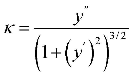 | (1) |
The theoretical performances for the HER of the flat and corrugated MoS2 monolayers were estimated from Gibbs free energy of adsorbed hydrogen (ΔGH*) in all Mo (molybdenum) and S (sulfur) sites using the single atom catalysis (SAC) approach.54 The ΔGH* in this approach is defined as
| ΔGH* = Eads + ΔEZPE − TΔSH* | (2) |
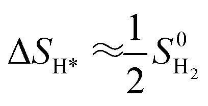 , where
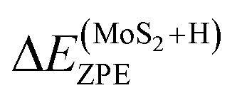
  is the entropy of gas phase H2 under standard conditions. In this work ΔEZPE for all Mo and S sites of corrugated MoS2, according to the following expression.
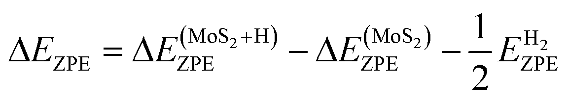 | (3) |
 is the zero-point energy of one hydrogen atom adsorbed on MoS2 monolayer,
 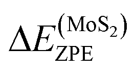 is the zero-point energy of the MoS2 monolayer and
 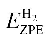 is the zero-point energy of the H2 molecule in the gas phase. Eads is the hydrogen binding energy and can be defined as
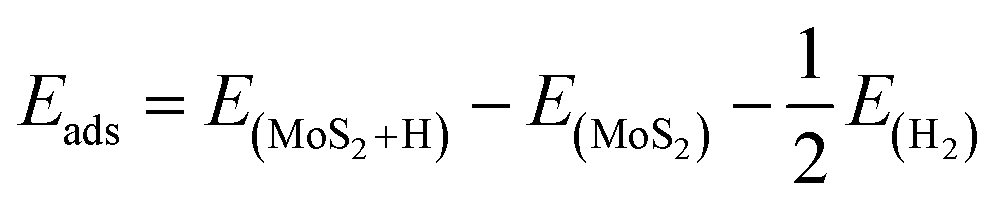 | (4) |
Results and discussion
Fig. 1a describes the fabrication process of the stretchable gold electrodes using PDMS as an elastomeric material. We fabricated holders using a 3D printer to keep the elastomer stretched at controlled levels. One of the challenges to fabricating stretchable conductive electrodes is to keep the thin metal films attached to PDMS due to the low surface energy of the polymer.55 Oxygen plasma treatment is widely employed to adjust PDMS surface properties.55,56 PDMS undergo chemical modifications on its surface, mainly by forming oxygenated chemical groups due to reaction with oxygen radicals.57 We confirmed the introduction of oxygen-rich functionalities by performing XPS analysis after the plasma treatment. Fig. S2† shows the formation of new Si–O and C–O groups on the surface. In addition, the overall chemical composition of oxygen increased by ≈100% (Table S1†). After plasma treatment, we immediately transfer the samples to the deposition chamber to prepare the conductive layer. After deposition of Ti/Au and strain release, the resulting electrode is flexible, as can be seen in Fig. 1b. In addition, due to preparation conditions, the electrode is stretchable. Fig. 1c(i and ii) illustrates a picture of the electrode and the wrinkled pattern observed after releasing the pre-strain. When a stiff film is attached to a pre-strained substrate, wrinkles are formed upon pre-strain release.58 By applying a tensile strain on the electrodes, as shown in Fig. 1c(iii and iv), the corrugated gold electrodes can be stretched by expanding the wavy-like patterns. To confirm that electrical properties were preserved after stretching we measured normalized conductance as a function of tensile strain, as illustrated in Fig. 1d. As can be observed, a minimal impact on the electrical properties up to ≈20% of strain highlights the stability of the conductive layer upon stretching.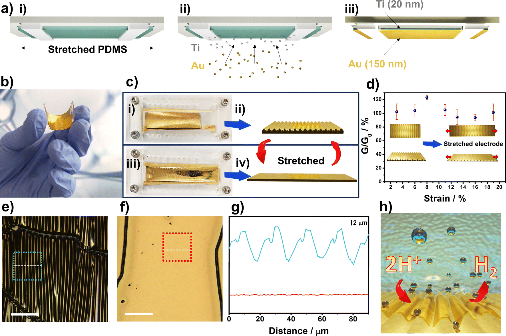 | ||
| Fig. 1 (a) Fabrication process of the stretchable gold electrodes: (i) PDMS substrates are stretched and subjected to oxygen plasma before the metallic layer deposition; (ii) Ti/Au layers deposition in electron beam chamber; (iii) stretchable gold electrode with Ti (20 nm) and Au (150 nm) layers. (b) Picture of the flexible and stretchable electrode fabricated. (c) (i) Picture of the stretchable electrode after releasing pre-strain; (ii) schematic representation of the wrinkled pattern of the surface; (iii) picture of the stretched gold electrode; (iv) schematic representation of the surface of the electrode after applying tensile strain. (d) Normalized conductance x tensile strain (%). LSCM images were obtained for the stretchable electrode (e) after releasing pre-strain and (f) with tensile strain applied. The scale bars in (e) and (f) are 100 μm long. (g) Linear profiles obtained from the indicated areas (blue and red squares in e and f, respectively). (h) Schematic representation of the expected HER improvement through the creation of new edge-like sites. | ||
The corrugated gold film that ensures high stretchability and preserves electrical properties can be better visualized in Fig. 1e and f by LSCM images. After pre-strain release, the elastomer returns to its unstrained state leading to the formation of wavy structures. The amplitude (A0) and wavelength (λ0) were 5.0 μm and 9.5 μm, respectively, by measuring the linear profiles on the LSCM images, as shown in Fig. 1g. The obtained values are higher when compared to other works, thus ensuring the stretchability of the wrinkled electrodes.59 When the electrodes are stretched, the wavelength and amplitude on the interface buckles gradually increased and decreased, respectively. Further stretching up to ≈25% of applied strain led to the formation of a flat gold film, as shown in Fig. 1g. Thus, considering that an effective strain up to 11% is necessary to promote the rupture of MoS2 monolayers,60 this work highlights a new method to introduce edge-like defects by applying uniaxial tensile strain at 20%. Since MoS2 edges are catalytic sites, it is expected an improved electrocatalytic activity toward HER after stretching the monolayers, as schematically shown in Fig. 1h.
The ultra-large MoS2 monolayers are prepared using a simple and fast electrochemical thinning method recently reported.43,44 This method is being reported for the first time on corrugated gold films. In brief, we transfer bulk flakes onto gold electrodes using sucrose. Fig. 2a shows the bulk MoS2 flakes adhered to the corrugated gold film. The light grey color indicates the multilayer nature of the layered material. After electrochemical thinning, the color of the MoS2 crystals changes to light yellow, thus confirming the reduction of layer number, as illustrated in Fig. 2b. The high magnification image of the ultra-large area thinned MoS2 layer can be visualized in Fig. 2c, where the monolayer adapts to the peaks and valleys of the curved surface. The large area of the basal plane is of fundamental importance for electrochemical studies on the basal plane, as will be shown ahead. Next, we employed LSCM to follow the introduction of edge-like defects on the basal plane on MoS2. The markers (*) and (**) in Fig. 2d indicate the peaks and the valleys of the wavy-like patterns, respectively. We created strain at the MoS2 monolayers by stretching the electrodes perpendicularly to the grooves. We held the electrode at 20% strain and obtained the image to highlight the cracks formed in this step. The edge-like defects follow the region of the valleys. Additional stretching cycles can be performed to tune the insertion of defects until the stage of bringing the electrode back to its unstrained initial condition.
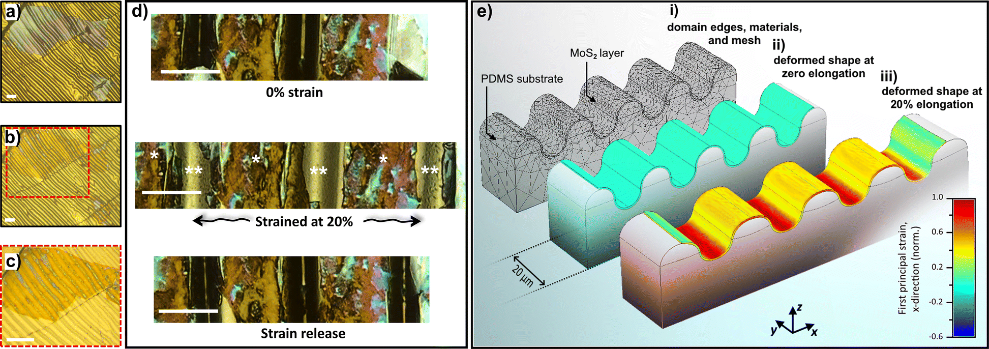 | ||
| Fig. 2 (a) Bulk MoS2 flake adhered onto the corrugated gold surface. (b) MoS2 monolayer on the gold surface after the electrochemical thinning process. Scale bars in panels a and b are 25 μm long. (c) High magnification image of the ultra-large thinned MoS2 layer from the squared region in b. Scale bar in c: 50 μm. (d) LSCM images obtained for thinned MoS2 (0% strain), after stretching the electrode at approximately 20% (strained at 20%) and after releasing the electrode from the stretching condition (strain release). Scale bars are 10 μm long, whereas (*) and (**) are the peak and valley of the wavy-like electrode, respectively. (e) Finite-element simulation of the strain-transfer properties within the wrinkled PDMS/MoS2 system. The system domain geometry considered in the calculation is composed of the MoS2 layer lying on the wrinkled surface of the stretchable substrate. (i) The domain edges, materials, and volumetric mesh configuration are showcased. For the calculation, the substrate was stretched along the x-axis direction, whereas the MoS2 layer strain compliance was computed at every small volume domain. The normalized first principal strain along the MoS2 layer (color scale) is shown at two substrate-stretching conditions: (ii) zero and (iii) 20% elongation. | ||
We conducted finite-element calculations to evaluate the structural mechanical properties related to the strain relaxation of the MoS2 layer. We were interested in the strain-transfer events that occur when the PDMS substrate is stretched, which may result in oriented cracks in the MoS2 layer. Our model consists of a MoS2 layer lying on a wrinkled PDMS substrate. Fig. 2e illustrates the simulation results with the sample geometry and calculated strain distributions. The material's volumetric domains and mesh structures are displayed in Fig. 2e(i). When the substrate is not stretched, the strain transferred to the MoS2 layer is negligible, as shown in Fig. 2e(ii). However, when the substrate is stretched, as indicated in Fig. 2e(iii), strain is transferred to the monolayer. The same figure shows that a strain gradient occurs in the MoS2 layer along the wrinkles of the PDMS substrate. Our calculations indicate that the edges of the MoS2 layer receive the least amount of strain transfer (≈20% of the maximum strain, as shown on the left or right-hand side of Fig. 2e(iii)). The peaks display intermediate strain transfer to the MoS2 layer, i.e., ≈50% of the maximum value achieved in the simulation. The substrate's valley regions experience the most critical amount of transferred strain. At this location, the MoS2 layer is subjected to the highest levels of mechanical stress upon substrate elongation (Fig. 2e(iii)). Therefore, our theoretical evaluation of the stretchable PDMS/MoS2 system suggests that valleys are more suitable for producing fractures in the MoS2 layers than the peaks or edge regions. As shown in Fig. 2e(iii), the formation of fractures is expected to follow the valley patterns, where the MoS2 layer may not display enough mechanical compliance to hold out the amount of transferred strain from the elongated PDMS. Our structural mechanics' findings reveal that the use of wrinkled-surface PDMS substrates may be a feasible way to produce well-oriented periodic cracks in MoS2 mono- and multilayers intentionally. In addition, the wavy-like patterns can be tuned using other experimental conditions, as shown in Fig. S3.†
One of the most used techniques to characterize MoS2 is Raman spectroscopy. By obtaining Raman spectra one can determine phase change,61 presence of defects,44,62 and number of layers.63Fig. 3a(i) shows the Raman spectra obtained in the basal plane of electrochemically thinned MoS2 attached to a flat Au electrode. The spectra show the presence of two main peaks in the range investigated, the E2g1(385.3 cm−1) and A1g (405.3 cm−1). The former corresponds to in-plane vibration while the latter is an out-of-plane Raman active mode of MoS2. The monolayer nature was confirmed by obtaining the frequency difference between the two modes. The obtained value was 20 cm−1, which is in agreement with reported values for monolayer MoS2.64 Next, we applied a uniaxial strain (≈20%) on the electrode and obtained Raman spectra on the basal plane located on the top of the peaks of the corrugated pattern, as shown in Fig. 3a(ii). The frequency difference below 21 cm−1 on the basal plane on the top of the peak (E2g1 − 385.2 cm−1 and A1g − 406.0), confirms the successful thinning process on MoS2 located on the wavy-like patterned electrode. After releasing the applied strain, we notice a red shift in both Raman peaks in the spectra in Fig. 3a(iii) (E2g1 − 383.0 cm−1 and A1g − 404.3). Such a shift is commonly associated with the presence of tensile strain in MoS2 layers.65 Raman maps at 20% of strain and after strain release are shown in Fig. 3b for the position of the E2g1 and A1g modes of MoS2 (Fig. 3b(i) and (ii), respectively). We employed the same location markers of Fig. 2d to identify the valleys and peaks of the electrode. By holding the electrode at 20% of strain we can observe the absence of Raman signal in the valleys due to the rupture of the monolayer, in agreement with the LSCM image illustrated in Fig. 2d. After strain release of the electrode, both E2g1 and A1g are red-shifted indicating that the area of the basal plane is strained (Fig. 3b(iii) and (iv), respectively).
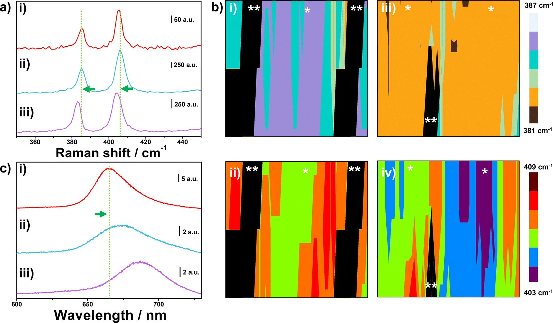 | ||
| Fig. 3 (a) Raman spectra of (i) MoS2 monolayer on a flat gold electrode; (ii) MoS2 monolayer on a stretched electrode (≈20%); (iii) MoS2 on a corrugated gold surface after strain releasing. (b) Raman maps of stretchable electrodes (i and ii) with uniaxial strain applied and (iii and iv) after releasing the strain. Panels i and iii refer to E2g1; panels ii and iv refer to A1g Raman modes. Raman maps are 37.4 μm × 2.1 μm. (c) Photoluminescence spectra of (i) MoS2 monolayer on a flat gold electrode; (ii) MoS2 monolayer on a stretched electrode (≈20%); (iii) MoS2 on a corrugated gold surface after strain releasing. | ||
Another way to confirm the monolayer nature of MoS2 and monitor the presence of strain is by using photoluminescence (PL) experiments. Due to changes in the electronic band gap from indirect (bulk) to direct (monolayer), the three-atom thick material presents remarkable photoluminescence when compared to multilayer MoS2.66Fig. 3c(i) shows the PL spectra obtained in the basal plane of MoS2 obtained in a flat electrode. A high-intensity peak located at 665 nm is attributed to exciton A, as reported for the MoS2 monolayer. In addition, the small peak at ≈620 nm that can be observed in the spectra is attributed to exciton B, as reported previously.67 Fig. S4† shows a zoom-in of the spectra in the ESI file† to highlight the presence of the small peak. From the PL spectra obtained on the basal plane located on the top of the peak at 20% of strain and after strain release, a red shift of the exciton A peak is observed in Fig. 3c(ii and iii), from 673 nm to 687 nm, respectively. These results align with the Raman experiments, which confirmed the presence of strain on the peaks of the wavy-like patterns. Another feature that highlights the influence of strain in the monolayer is the intensity of the exciton A peak.68 It has been reported that uniaxial tensile strain decreases the intensity of the A peak,29 which can also be seen in our case in Fig. 3c. In addition, the red shift in the PL peaks is an indication of the reduction of the band gap of MoS2 monolayer due to the applied strain.68 Thus, by applying and releasing strain in the Au-PDMS electrode it is possible to tune the band gap of MoS2.
A remarkable aspect of the defect-engineering step promoted by stretching the electrodes is that after releasing strain in PDMS, it promotes an additional influence of strain on the MoS2 monolayers, as confirmed by Raman and PL experiments. Compressive and tensile strain can be generated on MoS2 monolayers by manipulating the mechanical properties of the flexible substrate, i.e. bending or stretching the polymer.3 In our case, we observed a progressive red shift in Raman and PL spectra, which is indicative of tensile strain on the MoS2 monolayer.33,68–71 Uniaxial tensile strain on monolayer 2D materials has been observed on wrinkled structures formed on flexible65 and rigid72 substrates. Thus, we performed additional investigation to verify the formation of strained regions on the MoS2 basal plane. Fig. 4a shows the SEM image of the stretched electrode. It is possible to notice the presence of wrinkled structures on the basal plane of MoS2. To investigate topography changes, we obtained AFM images and line profiles on the top of the basal plane before and after the stretching process. Fig. 4b and c show the AFM image and the line profiles of the selected areas, respectively, after stretching and releasing strain on the substrate. The mapped region in Fig. 4b reveals that the basal plane contains many regions where the valley-to-peak distance is more pronounced. This feature can be better visualized in the line profiles illustrated in Fig. 4c, where many sharp regions indicated by the green arrows are seen in the graph. It is important to note that such “sharp” regions are not visualized on the MoS2 basal plane before the uniaxial tensile strain, as indicated by the control images illustrated in Fig. 4d and e. We inserted the AFM image and line profiles for the PDMS-Au in the SI file for comparison (Fig. S5†). Our results indicate that after stretching and releasing the electrode, wrinkles are formed on the basal plane, which explains the additional impact of strain detected by Raman and PL experiments.
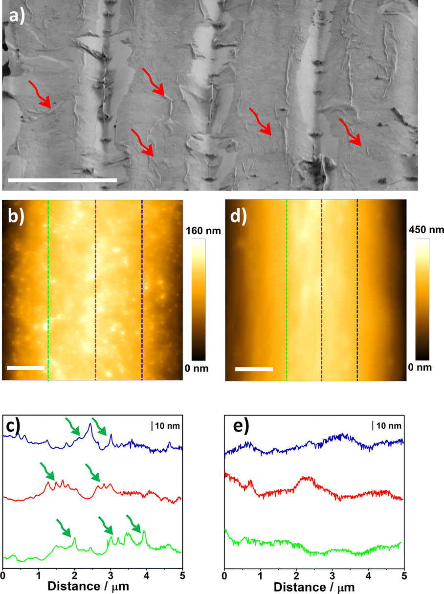 | ||
| Fig. 4 (a) SEM image of a MoS2 monolayer on a stretched electrode revealing cracks formation and wrinkled structure (red arrows). Scale bar: 25 μm. (b) AFM image of MoS2 monolayers after stretching and releasing the substrate. (c) Line profile of the indicated regions in panel b. Green arrows indicate sharp regions. (d) AFM image of a MoS2 on a stretchable electrode before subjecting to uniaxial tensile strain. (e) Line profile of the indicated regions in panel d. Scale bars in panels b and d: 1 μm. | ||
The introduction of valley-oriented edge-like defects on the basal plane of MoS2 by exploring the mechanical properties of stretchable electrodes is unique in this work. Other reported techniques can generate edge-like defects and fine-tune some properties of MoS2 monolayer. For example, by using an AFM tip and pressing a free-standing MoS2 monolayer it is possible to generate strain and induce crack formation.73 While strain can be fine-tuned using the tip, the direction of crack formation is hard to control on free-standing monolayers. On the other hand, defects on supported MoS2 monolayer can be achieved using thermochemical scanning probe lithography.74 High-resolution techniques such as transmission electron microscopy enable precise creation and observation of cracks on the basal plane,75 however, the technique is time-consuming and not appropriate for defect patterning in ultra-large areas. The most used patterning methods to generate active edges on MoS2 are based on lithography combined with wet or dry etching processes.76,77 In such methods, the photoresist or polymethyl methacrylate (PMMA) can cause contamination of the catalytic sites or undesirable oxidation.78,79 Another challenge is to assess the basal plane to measure the HER activity without contaminating the edge-like active sites.
To interrogate the MoS2 basal plane towards HER, we employed a recently reported two-step method to isolate only the region where the defects are introduced.44 In brief, the method consists of approaching an insulating resin with the aid of an optical microscope and curing the resin without the need to spread the material over the entire surface. Thus, the pristine and defect-engineered MoS2 basal plane can be evaluated without unintentional surface changes, as described above. Fig. 5a illustrates the overall schematic process for stretch-induced defects, microelectrode preparation, and electrochemical measurements. After stretching the electrodes, the resin was applied to isolate the basal plane. Fig. S6† shows the LSCM image of the electrode. The basal plane of the flat and corrugated MoS2 shows poor electrocatalytic activity due to the lack of active sites, as demonstrated by our DFT calculations below. However, after generating edge-like defects by stretching the electrodes, the overpotential to achieve 10 mA cm−2 was remarkably reduced to 352 mV (Fig. 5b). In addition, the stretched electrodes showed the lowest Tafel slopes, indicating faster kinetics in the HER process (Fig. 5c). Another key parameter when investigating the electrocatalytic activity of modified electrodes is long-term stability. We performed successive cycling using the defect-engineered electrode and observed that the electrode is stable up to 500 cycles, as seen in Fig. 5d. The slight improvement in the HER activity after cycling stability may be related to desulfurization of the basal plane.36 The Raman and PL spectra obtained on the region of the basal plane, showed the typical features of MoS2 after stretching and electrochemical long-term stability, as shown in Fig. S7.† Since minor changes were observed in Raman and PL spectra, XPS measurements were performed before and after cycling the electrodes, as illustrated in Fig. S8.† The results indicated an increased amount of oxidized Mo. As previously stated, MoS2 can react with oxygen under ambient conditions,80 in addition, wrinkles and strained regions present higher chemical reactivity.31 After stretching the samples, new edge sites and wrinkled regions are formed (Fig. 4a) which may favor the formation of additional active sites in MoS2 during electrochemical cycling. Such unintentional chemical changes may be favoring the increased reactivity in a small extent.
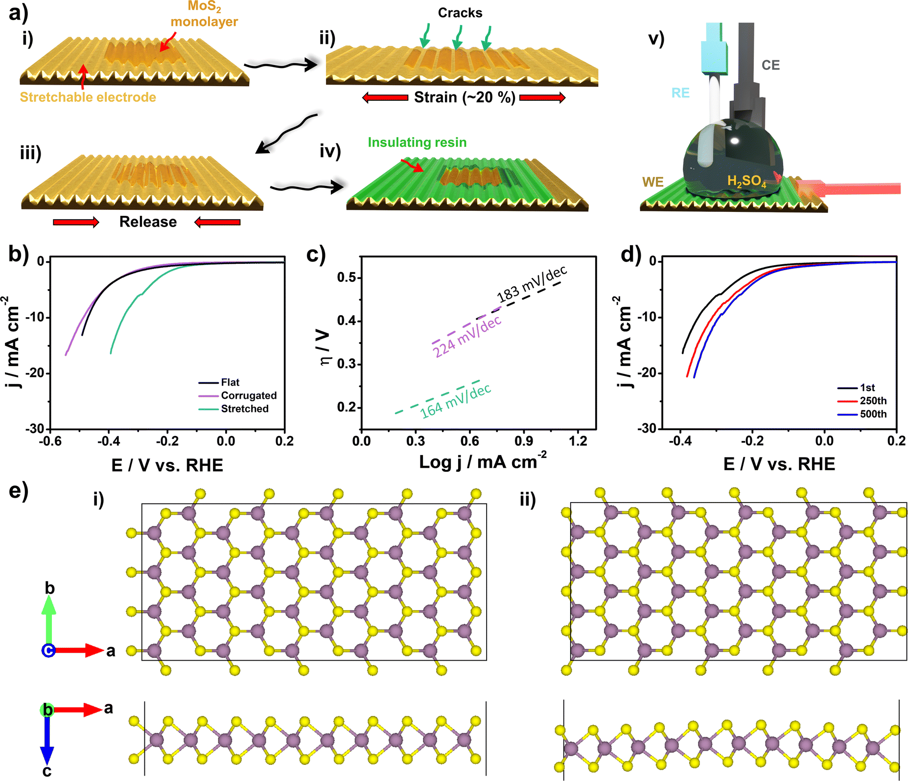 | ||
| Fig. 5 (a) Schematic representation of the electrode preparation and electrochemical experiments: (i) MoS2 onto stretchable gold electrodes after electrochemical thinning process; (ii) uniaxial tensile strain promotes the formation of cracks oriented in the “valley” regions of the surface; (iii) after the formation of cracks, the electrode is released from the tensile strain; (iv) an insulating resin is applied to isolate what was initially the basal plane; (v) the isolated microelectrode is applied as the working electrode in a three-electrode system and H2SO4 0.5 M solution is deposited to perform the measurements. (b) HER polarization curves obtained in H2SO4 0.5 M at 5 mV s−1. The surface topography was considered for the corrugated and stretched electrodes. (c) Tafel plots from the HER polarization curves. (d) Stability tests performed after 250 and 500 linear sweep voltammetry curves for the defective electrodes. (e) Top and side views of the optimized geometry of a 4 × 10 supercell for pristine (i) flat and (ii) corrugated MoS2 monolayers. The purple and yellow colors correspond to the atoms Mo and S, respectively. The a, b, and c axes of the supercells employed in this work are indicated at the bottom. The 1st scan in d is the same represented in b for the stretched sample. | ||
By observing the results shown in Fig. 5b, the stretched electrodes displayed the best performance among the three studied conditions due to the presence of edge-like defects, as described above. In addition, the edges created by stretching the electrodes are more stable than edges patterned by Ga+ beam44 and present superior electrocatalytic activity when compared to exposed edges tuned by O2 plasma etching.81 The enhancement of HER activity due to edge-like defects in MoS2 monolayers is well-documented.81–83 However, it may be surprising that curvature effects have very little effect in enhancing HER. To understand this behavior, we performed DFT calculations to understand the similar electrocatalytic activity between rigid and corrugated (not stretched) MoS2 monolayers. For this analysis, flat and corrugated MoS2 monolayers, both pristine, were built and can be seen in Fig. 5e. It is well-known that for an ideal hydrogen catalyst, the Gibbs free energy of hydrogen adsorption (ΔGH*) should be approximately zero (ΔGH* ≈ 0),84 since the overpotential (η) is related to ΔGH* by η = |ΔGH*|/e,85 where e is the elementary charge. Thus, we determine the HER activity of the flat and corrugated MoS2 monolayers by calculating the ΔGH* in the single atom catalyst (SAC) approach54 for all molybdenum (Mo-) and sulfur (S-) sites in the model structures (see Fig. 5e). For the flat MoS2 (Fig. 5e(i)) monolayer we find that |ΔGMoH*| ≈ 2.1 eV for the Mo-sites and |ΔGSH*| ≈ 1.76 eV for the S-sites, and which are in agreement with the results found in the literature.18,20 In the case of corrugated MoS2 monolayer (Fig. 5e(ii)), we obtain respectively |ΔGMoH*| ≈ 2.3 and |ΔGSH*| ≈ 1.82 eV. Therefore, there is no substantial variation of Gibbs free energies due to curvature alone, in agreement with HER polarization curves, where in both cases (flat and corrugated) HER polarization have the same behavior and do not exhibit good HER efficiency. These results show that the corrugation does not have influence in HER efficiency for pristine systems. In the case of stretched MoS2 monolayer, the best performance in HER is related to the formation of edge-like defects in the basal plane.
Conclusions
In conclusion, we reported for the first time the formation of edge-like defects in ultra-large MoS2 monolayers by stretching gold electrodes. The wavy-like electrodes can be stretched up to 20% with minimal impact on their electrical properties, thus ensuring proper conditions for the defect engineering step. The electrochemical thinning process enables the fast and simple preparation of ultra-large area MoS2 monolayers attached to the corrugated electrodes. By applying uniaxial tensile strain exceeding the mechanical compliance of MoS2 monolayers, the generation of oriented cracks that follow the valleys of the electrode was demonstrated. Simulations confirmed that the regions on the bottom of the valleys were more prone to crack, due to the large strain in this region. Raman and PL experiments confirmed the presence of strained areas after stretching the electrodes, and such strained regions were attributed to the formation of wrinkled regions as shown by SEM and AFM images. The electrocatalytic activity of the electrodes was measured by isolating only the basal plane, and a remarkable decrease of overpotential to 352 mV was observed when measured at 10 mA cm−2. In addition, the electrodes are stable after long-term cycling. DFT studies reveal that curvature alone has minor effects on HER activity since the Gibbs free energy of adsorption was similar comparing flat and corrugated electrodes without defects, in agreement with experiments.Our route opens a new possibility to generate edge-like defects on MoS2 monolayers by stretching the electrodes. The fabrication method is scalable, and the area of the electrodes can be further tuned. While significant effort has been made using MoS2 monolayers for stretchable electronics,86–88 this is the first work that illustrates key features to create defects and improve the electrocatalytic activity of stretchable electrodes. Thus, we expect that this toolbox can be expanded to other 2D materials and drive discoveries in the field. We believe that by making some adjustments it will be possible to perform bi-axial strain to increase the number of defects and/or create other corrugated patterns. Further work will be undertaken by combining the mechanical properties of the electrode and defect-engineering steps on the basal plane.
Data availability
All data obtained will be stored on the researcher's personal computer, in cloud services (One Drive), and in the repository of the Brazilian Center for Research in Energy and Materials (CNPEM). Files saved in the three locations above described will be organized as follows: technique > measurement date > sample > experimental conditions, to facilitate quick location. Records noted as sample preparation and experimental conditions will be made in an laboratory notebook that belongs to the research center, which will be available for internal and external consultation. Additional data were also inserted in the ESI file. †Author contributions
L. H. H performed the fabrication, transfer process, electrochemical studies, and wrote the manuscript. C. L and A. B. S. A contributed to experimental procedures and characterization of the electrodes. G. C. and R. B. C. contributed to computational studies. L. M. contributed to the structural mechanics simulation. E. R. L. contributed to discussions. M. S. conceived the idea, designed the experiments, and wrote the manuscript.Conflicts of interest
There are no conflicts of interest to declare.Acknowledgements
This work was supported by the Serrapilheira Institute (grant number: Serra-1912-31228), São Paulo Research Foundation (FAPESP), and INCT – Materials Informatics and INCT – Carbon Nanomaterials. L. H. H. thanks São Paulo Research Foundation – FAPESP for the scholarship (grant number: 2022/00955-0). L. M. acknowledges the support from the Freistaat Sachsen through the Professorship of Materials Systems for Nanoelectronics at the Chemnitz University of Technology. We thank Fabiano E. Montoro, Mariane P. Pereira, Carolina P. Torres, Carlos A. R. Costa, and Cleyton A. Biffe for their help in this work with instrumentation and laboratory facilities. G. C. gratefully acknowledges FAPERJ, grant number E-26/200.627/2022 and E-26/210.391/2022 (project Jovem Pesquisador Fluminense process number 271814) for financial support. The authors thank Sistema Nacional de Processamento de Alto Desempenho (SINAPAD/SDUMONT) and Centro Nacional de Processamento de Alto Desempenho em São Paulo (CENAPADSP) for computational support. We also thank SisNano for the support.References
- W. Wu, Sci. Technol. Adv. Mater., 2019, 20, 187–224 CrossRef CAS.
- L. Merces, L. M. M. Ferro, A. Thomas, D. D. Karnaushenko, Y. Luo, A. I. Egunov, W. Zhang, V. K. Bandari, Y. Lee, J. S. McCaskill, M. Zhu, O. G. Schmidt and D. Karnaushenko, Adv. Mater., 2024, 2313327 CrossRef PubMed.
- S. Deng, A. V. Sumant and V. Berry, Nano Today, 2018, 22, 14–35 CrossRef CAS.
- X. Cao, D. Tan, Q. Guo, T. Zhang, F. Hu, N. Sun, J. Huang, C. Fang, R. Ji, S. Bi and C. Jiang, J. Mater. Chem. A, 2022, 10, 11562–11573 RSC.
- G. Shao, R. Yu, N. Chen, M. Ye and X. Y. Liu, Small Methods, 2021, 5, 2000853 CrossRef CAS PubMed.
- Q. Wan, S. Seo, S.-W. Lee, J. Lee, H. Jeon, T.-S. Kim, B. J. Kim and B. C. Thompson, J. Am. Chem. Soc., 2023, 145, 11914–11920 CrossRef CAS PubMed.
- Q. Zhai, Y. Liu, R. Wang, Y. Wang, Q. Lyu, S. Gong, J. Wang, G. P. Simon and W. Cheng, Adv. Energy Mater., 2020, 10, 1903512 CrossRef CAS.
- Y. Liu, K. He, G. Chen, W. R. Leow and X. Chen, Chem. Rev., 2017, 117, 12893–12941 CrossRef CAS PubMed.
- K. S. Kim, Y. Zhao, H. Jang, S. Y. Lee, J. M. Kim, K. S. Kim, J.-H. Ahn, P. Kim, J.-Y. Choi and B. H. Hong, Nature, 2009, 457, 706–710 CrossRef CAS PubMed.
- J. Miao and T. Fan, Carbon, 2023, 202, 495–527 CrossRef CAS.
- Y. Han, B. Park, J. Eom, V. Jella, S. Ippili, S. V. N. Pammi, J. Choi, H. Ha, H. Choi, C. Jeon, K. Park, H. Jung, S. Yoo, H. Y. Kim, Y. H. Kim and S. Yoon, Advanced Science, 2021, 8, 2003697 CrossRef CAS PubMed.
- E. Chen, W. Xu, J. Chen and J. H. Warner, Mater. Today Adv., 2020, 7, 100076 CrossRef.
- G. Shao, X.-X. Xue, X. Zhou, J. Xu, Y. Jin, S. Qi, N. Liu, H. Duan, S. Wang, S. Li, M. Ouzounian, T. S. Hu, J. Luo, S. Liu and Y. Feng, ACS Nano, 2019, 13, 8265–8274 CrossRef CAS PubMed.
- G. Shao, X. Xue, B. Wu, Y. Lin, M. Ouzounian, T. S. Hu, Y. Xu, X. Liu, S. Li, K. Suenaga, Y. Feng and S. Liu, Adv. Funct. Mater., 2020, 30, 1906069 CrossRef CAS.
- G. Shao, Y. Lu, J. Hong, X. Xue, J. Huang, Z. Xu, X. Lu, Y. Jin, X. Liu, H. Li, S. Hu, K. Suenaga, Z. Han, Y. Jiang, S. Li, Y. Feng, A. Pan, Y. Lin, Y. Cao and S. Liu, Adv. Sci., 2020, 7, 2002172 CrossRef CAS PubMed.
- G. Barik and S. Pal, J. Phys. Chem. C, 2019, 123, 21852–21865 CrossRef CAS.
- Z. Wu, B. Li, Y. Xue, J. Li, Y. Zhang and F. Gao, J. Mater. Chem. A, 2015, 3, 19445–19454 RSC.
- J. Xu, G. Shao, X. Tang, F. Lv, H. Xiang, C. Jing, S. Liu, S. Dai, Y. Li, J. Luo and Z. Zhou, Nat. Commun., 2022, 13, 2193 CrossRef CAS PubMed.
- L. H. Hasimoto, J. Bettini, E. R. Leite, R. S. Lima, J. B. Souza Junior, L. Liu and M. Santhiago, ACS Appl. Eng. Mater., 2023, 1, 708–719 CrossRef CAS.
- L. Lin, P. Sherrell, Y. Liu, W. Lei, S. Zhang, H. Zhang, G. G. Wallace and J. Chen, Adv. Energy Mater., 2020, 10, 1903870 CrossRef CAS.
- G. Shao, M. Yang, H. Xiang, S. Luo, X.-X. Xue, H. Li, X. Zhang, S. Liu and Z. Zhou, Nano Res., 2023, 16, 1670–1678 CrossRef CAS.
- G. Shao, H. Xiang, M. Huang, Y. Zong, J. Luo, Y. Feng, X.-X. Xue, J. Xu, S. Liu and Z. Zhou, Sci. China Mater., 2022, 65, 1833–1841 CrossRef CAS.
- X. Wang, Y. Zhang, H. Si, Q. Zhang, J. Wu, L. Gao, X. Wei, Y. Sun, Q. Liao, Z. Zhang, K. Ammarah, L. Gu, Z. Kang and Y. Zhang, J. Am. Chem. Soc., 2020, 142, 4298–4308 CrossRef CAS PubMed.
- C. Tsai, H. Li, S. Park, J. Park, H. S. Han, J. K. Nørskov, X. Zheng and F. Abild-Pedersen, Nat. Commun., 2017, 8, 15113 CrossRef PubMed.
- Z. Huang, W. Deng, Z. Zhang, B. Zhao, H. Zhang, D. Wang, B. Li, M. Liu, Y. Huangfu and X. Duan, Adv. Mater., 2023, 35, 2211252 CrossRef CAS PubMed.
- H. Zhu, X. Qin, L. Cheng, A. Azcatl, J. Kim and R. M. Wallace, ACS Appl. Mater. Interfaces, 2016, 8, 19119–19126 CrossRef CAS PubMed.
- P. Zhang, H. Xiang, L. Tao, H. Dong, Y. Zhou, T. S. Hu, X. Chen, S. Liu, S. Wang and S. Garaj, Nano Energy, 2019, 57, 535–541 CrossRef CAS.
- K. K. Amara, L. Chu, R. Kumar, M. Toh and G. Eda, APL Mater., 2014, 2, 092509 CrossRef.
- Z. Li, Y. Lv, L. Ren, J. Li, L. Kong, Y. Zeng, Q. Tao, R. Wu, H. Ma, B. Zhao, D. Wang, W. Dang, K. Chen, L. Liao, X. Duan, X. Duan and Y. Liu, Nat. Commun., 2020, 11, 1151 CrossRef CAS PubMed.
- S. Bolar, S. Shit, N. C. Murmu, P. Samanta and T. Kuila, ACS Appl. Mater. Interfaces, 2021, 13, 765–780 CrossRef CAS PubMed.
- J. Wang, L. He, Y. Zhang, H. Nong, S. Li, Q. Wu, J. Tan and B. Liu, Adv. Mater., 2024, 2314145 CrossRef CAS PubMed.
- S. Yang, Y. Chen and C. Jiang, InfoMat, 2021, 3, 397–420 CrossRef.
- H. Li, M. Du, M. J. Mleczko, A. L. Koh, Y. Nishi, E. Pop, A. J. Bard and X. Zheng, J. Am. Chem. Soc., 2016, 138, 5123–5129 CrossRef CAS PubMed.
- C. Di Giorgio, E. Blundo, G. Pettinari, M. Felici, A. Polimeni and F. Bobba, ACS Appl. Mater. Interfaces, 2021, 13, 48228–48238 CrossRef CAS PubMed.
- X. Liu, Z. Li, H. Jiang, X. Wang, P. Xia, Z. Duan, Y. Ren, H. Xiang, H. Li, J. Zeng, Y. Zhou and S. Liu, Small, 2023, 2307293 Search PubMed.
- D. Rhuy, Y. Lee, J. Y. Kim, C. Kim, Y. Kwon, D. J. Preston, I. S. Kim, T. W. Odom, K. Kang, D. Lee and W.-K. Lee, Nano Lett., 2022, 22, 5742–5750 CrossRef CAS PubMed.
- J. H. Lee, W. S. Jang, S. W. Han and H. K. Baik, Langmuir, 2014, 30, 9866–9873 CrossRef CAS PubMed.
- H. Xing, X. Wang, C. Xu, H. Du, R. Li, Z. Zhao and W. Qiu, Carbon, 2023, 204, 566–574 CrossRef CAS.
- N. Basu, R. Kumar, D. Manikandan, M. Ghosh Dastidar, P. Hedge, P. K. Nayak and V. P. Bhallamudi, RSC Adv., 2023, 13, 16241–16247 RSC.
- Z. Liu, M. Amani, S. Najmaei, Q. Xu, X. Zou, W. Zhou, T. Yu, C. Qiu, A. G. Birdwell, F. J. Crowne, R. Vajtai, B. I. Yakobson, Z. Xia, M. Dubey, P. M. Ajayan and J. Lou, Nat. Commun., 2014, 5, 5246 CrossRef PubMed.
- W. Chen, Y. Qiu, I. S. Babichuk, Y. Chang, R. Zhou, Z. He, Y. Liu, J. Zhang, I. V. Babichuk, A. Tiutiunnyk, D. Laroze, V. V. Brus and J. Yang, Adv. Eng. Mater., 2023, 2301470 Search PubMed.
- G. Li, Z. Chen, Y. Li, D. Zhang, W. Yang, Y. Liu and L. Cao, ACS Nano, 2020, 14, 1707–1714 CrossRef CAS PubMed.
- N. de Freitas, B. R. Florindo, V. M. S. Freitas, M. H. de O. Piazzetta, C. A. Ospina, J. Bettini, M. Strauss, E. R. Leite, A. L. Gobbi, R. S. Lima and M. Santhiago, Nanoscale, 2022, 14, 6811–6821 RSC.
- B. R. Florindo, L. H. Hasimoto, N. De Freitas, G. Candiotto, E. N. Lima, C. De Lourenço, A. B. S. De Araujo, C. Ospina, J. Bettini, E. R. Leite, R. S. Lima, A. Fazzio, R. B. Capaz and M. Santhiago, J. Mater. Chem. A, 2023, 11, 19890–19899 RSC.
- S. Damasceno, C. C. Corrêa, R. F. Gouveia, M. Strauss, C. C. B. Bufon and M. Santhiago, Adv. Electron. Mater., 2019, 6, 1900826 CrossRef.
- L. Merces, R. F. De Oliveira and C. C. Bof Bufon, ACS Appl. Mater. Interfaces, 2018, 10, 39168–39176 CrossRef CAS PubMed.
- W. Kohn and L. J. Sham, Phys. Rev., 1965, 140, A1133–A1138 CrossRef.
- G. Kresse and J. Furthmüller, Phys. Rev. B: Condens. Matter Mater. Phys., 1996, 54, 11169–11186 CrossRef CAS PubMed.
- J. Hafner, J. Comput. Chem., 2008, 29, 2044–2078 CrossRef CAS PubMed.
- J. P. Perdew, K. Burke and M. Ernzerhof, Phys. Rev. Lett., 1996, 77, 3865–3868 CrossRef CAS PubMed.
- P. E. Blöchl, Phys. Rev. B: Condens. Matter Mater. Phys., 1994, 50, 17953–17979 CrossRef PubMed.
- G. Kresse and D. Joubert, Phys. Rev. B: Condens. Matter Mater. Phys., 1999, 59, 1758–1775 CrossRef CAS.
- H. J. Monkhorst and J. D. Pack, Phys. Rev. B: Solid State, 1976, 13, 5188–5192 CrossRef.
- J. K. Nørskov, T. Bligaard, A. Logadottir, J. R. Kitchin, J. G. Chen, S. Pandelov and U. Stimming, J. Electrochem. Soc., 2005, 152, J23 CrossRef.
- D. W. Kim, M. Kong and U. Jeong, Adv. Sci., 2021, 8, 2004170 CrossRef PubMed.
- C.-Y. Li and Y.-C. Liao, ACS Appl. Mater. Interfaces, 2016, 8, 11868–11874 CrossRef CAS PubMed.
- B. Jiang, H. Guo, D. Chen and M. Zhou, Appl. Surf. Sci., 2022, 574, 151704 CrossRef CAS.
- Y. Ma, Y. Xue, K.-I. Jang, X. Feng, J. A. Rogers and Y. Huang, Proc. R. Soc. A, 2016, 472, 20160339 CrossRef PubMed.
- B. Wang, S. Bao, S. Vinnikova, P. Ghanta and S. Wang, npj Flexible Electron., 2017, 1, 5 CrossRef.
- S. Bertolazzi, J. Brivio and A. Kis, ACS Nano, 2011, 5, 9703–9709 CrossRef CAS PubMed.
- N. Moses Badlyan, N. Pettinger, N. Enderlein, R. Gillen, X. Chen, W. Zhang, K. C. Knirsch, A. Hirsch and J. Maultzsch, Phys. Rev. B, 2022, 106, 104103 CrossRef CAS.
- K. Ye, K. Li, Y. Lu, Z. Guo, N. Ni, H. Liu, Y. Huang, H. Ji and P. Wang, TrAC, Trends Anal. Chem., 2019, 116, 102–108 CrossRef CAS.
- C. Lee, H. Yan, L. E. Brus, T. F. Heinz, J. Hone and S. Ryu, ACS Nano, 2010, 4, 2695–2700 CrossRef CAS PubMed.
- H. Li, Q. Zhang, C. C. R. Yap, B. K. Tay, T. H. T. Edwin, A. Olivier and D. Baillargeat, Adv. Funct. Mater., 2012, 22, 1385–1390 CrossRef CAS.
- A. Castellanos-Gomez, R. Roldán, E. Cappelluti, M. Buscema, F. Guinea, H. S. J. Van Der Zant and G. A. Steele, Nano Lett., 2013, 13, 5361–5366 CrossRef CAS PubMed.
- K. F. Mak, C. Lee, J. Hone, J. Shan and T. F. Heinz, Phys. Rev. Lett., 2010, 105, 136805 CrossRef PubMed.
- K. K. Paul, L. P. L. Mawlong and P. K. Giri, ACS Appl. Mater. Interfaces, 2018, 10, 42812–42825 CrossRef CAS PubMed.
- H. J. Conley, B. Wang, J. I. Ziegler, R. F. Haglund, S. T. Pantelides and K. I. Bolotin, Nano Lett., 2013, 13, 3626–3630 CrossRef CAS PubMed.
- C. K. Tan, W. C. Wong, S. M. Ng, H. F. Wong, C. W. Leung and C. L. Mak, Vacuum, 2018, 153, 274–276 CrossRef CAS.
- C. Rice, R. J. Young, R. Zan, U. Bangert, D. Wolverson, T. Georgiou, R. Jalil and K. S. Novoselov, Phys. Rev. B: Condens. Matter Mater. Phys., 2013, 87, 081307 CrossRef.
- H. Li, A. W. Contryman, X. Qian, S. M. Ardakani, Y. Gong, X. Wang, J. M. Weisse, C. H. Lee, J. Zhao, P. M. Ajayan, J. Li, H. C. Manoharan and X. Zheng, Nat. Commun., 2015, 6, 7381 CrossRef CAS PubMed.
- N. Sakai, M. Suzuki and T. Sasaki, Adv. Mater. Interfaces, 2022, 9, 2102591 CrossRef CAS.
- Y. Manzanares-Negro, G. López-Polín, K. Fujisawa, T. Zhang, F. Zhang, E. Kahn, N. Perea-López, M. Terrones, J. Gómez-Herrero and C. Gómez-Navarro, ACS Nano, 2021, 15, 1210–1216 CrossRef CAS PubMed.
- X. Zheng, A. Calò, T. Cao, X. Liu, Z. Huang, P. M. Das, M. Drndic, E. Albisetti, F. Lavini, T.-D. Li, V. Narang, W. P. King, J. W. Harrold, M. Vittadello, C. Aruta, D. Shahrjerdi and E. Riedo, Nat. Commun., 2020, 11, 3463 CrossRef CAS PubMed.
- T. H. Ly, J. Zhao, M. O. Cichocka, L.-J. Li and Y. H. Lee, Nat. Commun., 2017, 8, 14116 CrossRef CAS PubMed.
- H. Park, J. Lee, G. Han, A. AlMutairi, Y.-H. Kim, J. Lee, Y.-M. Kim, Y. J. Kim, Y. Yoon and S. Kim, Commun. Mater., 2021, 2, 94 CrossRef CAS.
- X. Wang, J. Wu, Y. Zhang, Y. Sun, K. Ma, Y. Xie, W. Zheng, Z. Tian, Z. Kang and Y. Zhang, Adv. Mater., 2023, 35, 2206576 CrossRef CAS PubMed.
- P. K. Poddar, Y. Zhong, A. J. Mannix, F. Mujid, J. Yu, C. Liang, J.-H. Kang, M. Lee, S. Xie and J. Park, Nano Lett., 2022, 22, 726–732 CrossRef CAS PubMed.
- J. Liang, K. Xu, B. Toncini, B. Bersch, B. Jariwala, Y. Lin, J. Robinson and S. K. Fullerton-Shirey, Adv. Mater. Interfaces, 2019, 6, 1801321 CrossRef.
- J. Pető, T. Ollár, P. Vancsó, Z. I. Popov, G. Z. Magda, G. Dobrik, C. Hwang, P. B. Sorokin and L. Tapasztó, Nat. Chem., 2018, 10, 1246–1251 CrossRef PubMed.
- G. Ye, Y. Gong, J. Lin, B. Li, Y. He, S. T. Pantelides, W. Zhou, R. Vajtai and P. M. Ajayan, Nano Lett., 2016, 16, 1097–1103 CrossRef CAS PubMed.
- J. Zhang, D. Li, L. Ju, G. Yang, D. Yuan, Z. Feng and W. Wang, Phys. Chem. Chem. Phys., 2023, 25, 10956–10965 RSC.
- Z. H. Tan, X. Y. Kong, B.-J. Ng, H. S. Soo, A. R. Mohamed and S.-P. Chai, ACS Omega, 2023, 8, 1851–1863 CrossRef CAS PubMed.
- S. B. Saseendran, A. Ashok and A. A. S, Int. J. Hydrogen Energy, 2022, 47, 9579–9592 CrossRef CAS.
- H. Ooka, J. Huang and K. S. Exner, Front. Energy Res., 2021, 9, 654460 CrossRef.
- W. Zhang, Y. Liu, X. Pei, Z. Yuan, Y. Zhang, Z. Zhao, H. Hao, R. Long and N. Liu, Adv. Funct. Mater., 2022, 32, 2107524 CrossRef CAS.
- J. Li, N. Li, Q. Wang, Z. Wei, C. He, D. Shang, Y. Guo, W. Zhang, J. Tang, J. Liu, S. Wang, W. Yang, R. Yang, D. Shi and G. Zhang, Adv. Electron. Mater., 2022, 8, 2200238 CrossRef CAS.
- H. Kim, H. L. Zhao and A. M. Van Der Zande, Nano Lett., 2024, 24, 1454–1461 CrossRef CAS PubMed.
Footnote |
| † Electronic supplementary information (ESI) available: Additional DFT, XPS, PL, Raman, and characterization studies. See DOI: https://doi.org/10.1039/d4ta02042a |
| This journal is © The Royal Society of Chemistry 2024 |