
Time- and momentum-resolved image-potential states of 2H-MoS2 surface†
Jianyi
Liu
,
Xiang
Jiang
,
Xintong
Li
,
Xiaochuan
Ma
,
Xia
Sun
 ,
Qijing
Zheng
,
Xuefeng
Cui
*,
Shijing
Tan
,
Jin
Zhao
* and
Bing
Wang
*
,
Qijing
Zheng
,
Xuefeng
Cui
*,
Shijing
Tan
,
Jin
Zhao
* and
Bing
Wang
*
Hefei National Laboratory for Physical Sciences at the Microscale and Synergetic Innovation Center of Quantum Information & Quantum Physics, CAS Key Laboratory of Strongly-Coupled Quantum Matter Physics, and Department of Physics, University of Science and Technology of China, Hefei, Anhui 230026, China. E-mail: xfcui@ustc.edu.cn; zhaojin@ustc.edu.cn; bwang@ustc.edu.cn
First published on 2nd November 2021
Abstract
Rydberg-like image potential states (IPSs) form special series surface states on metal and semiconducting surfaces. Here, using time-resolved and momentum-resolved multi-photon photoemission (mPPE), we measured the energy positions, band dispersion, and carrier lifetimes of IPSs at the 2H-MoS2 surface. The energy minima of the IPSs (n = 1 and 2) were located at 0.77 and 0.21 eV below the vacuum level. In addition, the effective masses of these two IPSs are close to the rest mass of the free electron, clearly showing nearly-free-electron character. These properties suggest a good screening effect in the MoS2 parallel to the surface. The multi-photon resonances between the valence band and IPS (n = 1) are observed, showing a k‖-momentum-dependent behavior. Our time-resolved mPPE measurements show that the lifetime of photoexcited electrons in the IPS (n = 1) is about 33 fs.
1. Introduction
Rydberg-like image potential states (IPSs) form a special class of electronic states at different surfaces where they are bound by their image charges through the long-range Coulomb interaction. IPSs at metal surfaces have been intensively studied since 1985,1 and they have also been observed at semiconducting surfaces.2,3 As a special series of surface states, IPSs are extremely sensitive to surface properties. They are bound by the electrostatic Coulomb potential and reside few angstroms outside the surface, making them particularly alert to changes in the surface electrostatic potential. For example, with molecules or atoms adsorbed on the surface, interfacial charge transfer or reorienting molecular dipoles in the adsorbate layer can change the surface dipoles, which will affect the energy positions of the IPSs.4–6 Furthermore, the molecular layer on metal surfaces can be considered as a quantum well, which confines the image wavefunction by the thickness of the adsorbate layer.7,8 Moreover, the IPSs may couple strongly to the other electronic bands through photoexcitation. As a series of unoccupied states, they have been reported to be mediated states for charge transfer dynamics at different interfaces.9–12 Therefore, the measurement of IPSs, especially the dynamics of IPSs, is of great importance to understand the dynamics on the surface.Compared to traditional metal surfaces, the newly developed two-dimensional (2D) material family brings new chances for novel optoelectronic devices, in which the charge transfer dynamics play a key role.13–15 The measurement of IPS dynamics on 2D materials will provide an approach to investigate the charge transfer dynamics at the surfaces and interfaces of 2D materials. In addition, unlike those electronic states that usually have a density distribution localized around the nuclei, the maxima of IPSs are located away from the atomic centers; namely, they have nonnuclear density maxima, showing diffusive character and forming energy bands with nearly-free-electron (NFE) character.16–18 Such NFE-like IPSs are expected to exist in low-dimensional nanomaterials. For example, the existence of IPSs in two-dimensional (2D) graphene was theoretically predicted.19–21 When 2D graphene is wrapped to form a one-dimensional (1D) carbon nanotube or zero-dimensional (0D) fullerenes, the IPSs can transfer into the 1D NFE states or 0D superatom molecular orbitals.22–24 All these states have nonnuclear density maxima, which were proposed to have small electron–phonon interactions and to provide unique conduction channels.25 Therefore, it is also of great interest to understand the properties of IPSs in low-dimensional materials,21,26 especially in the newly developed 2D-materials family.27
Transition metal dichalcogenides (TMDs) form one of the most intensively studied 2D semiconductor families, which have important applications in spintronics and optoelectronics.14,15,28–30 Extensive research efforts have been performed on their electronic structures, charge carrier dynamics and light–matter interaction.31–35 The energy positions and band dispersion of IPS are related to 2D screening properties. The electron can be excited into the IPS by photons. Such photoexcited electrons with a certain lifetime on IPS can scatter with phonons and other charge carriers during its relaxation, which will affect the photoexcited charge carrier dynamics on TMD surface.33
MoS2 is a representative material in various TMDs. Bulk 2H-MoS2 is an indirect gap semiconductor with a bandgap of about 1.29 eV,32 which is different from monolayer MoS2 with a direct bandgap of about 1.8 eV.36 Despite their difference in the bandgaps, understanding the electron dynamics of the IPSs in bulk 2H-MoS2 should be an important step for further understanding of other competing dynamical properties in less-layered MoS2 and even TMD materials.37 Many studies have been carried out on the dynamics of excited states in conduction bands or intervalley scattering in MoS2.31,33–35,38 However, to our best knowledge, we are unaware of any report on the dynamical properties of trapped electrons in MoS2 IPSs, and it is even unclear if there exist resolvable IPSs at MoS2 surfaces.
In this work, we, for the first time investigate the hot electron dynamics of IPSs at bulk 2H-MoS2 surface by means of time-resolved and momentum-resolved multi-photon photoemission (TR-MR-mPPE) spectroscopy, with m = 3, 4, and 5 using varying the photon energies. Scanning tunneling microscopy (STM) and conventional angle-resolved photoemission spectroscopy (ARPES) were also used for characterizing the surface morphology and the valence band structure of the 2H-MoS2 surface. In our results, the observed parabolic dispersion of the states near the vacuum level of the 2H-MoS2 surface can be well described by a series of Rydberg-like image potential states, in good agreement with the features of IPSs. The observed effective masses of electrons in the IPSs are very close to the rest mass of a free electron. These features are well supported by our theoretical calculations. Multiphoton excitation processes are identified, and the momentum-dependent resonances between IPS and the valence band maximum (VBM) are observed. The lifetime of the 2H-MoS2 IPS was also measured.
2. Experimental and theoretical
The experiments were carried out in an ultrahigh vacuum (UHV) system equipped with a low-temperature scanning tunneling microscope (LT-STM, Omicron), and a TR-MR-mPPE system, similar to the system developed by Reutzel et al.,39 that recorded spectra using a hemispherical electron energy analyzer (SPECS PHOIBOS 150) with a 2D delay-line detector (DLD). The base pressure of the system was better than 2 × 10⁻¹⁰ mbar. The photo-excitation source for the mPPE measurements was a noncollinear parametric amplifier (NOPA) system pumped by a Clark MXR Impulse fiber laser. The NOPA system was performed at a power of about 10 μJ pulse−1 with a repetition rate of 500 kHz and a tunable wavelength in the range of 340–900 nm (pulse width ≈30 fs after compensation with a compressor). The p-polarized laser light with an incident angle of 45° from the surface normal was used, with a focused beam size of about 50 μm at the sample surface. In the interferometric measurements, identical pump–probe pulse pairs were generated using a Mach-Zehnder interferometer,40 and the delay time was scanned using a piezo driver that electrically varies the path length of one arm. One output of the interferometer was directly focused onto the sample as the mPPE excitation source, while the other one was transmitted through a monochromator to generate interference fringes that calibrate the pump–probe delay time.12 More than 200 pump–probe scans were accumulated to improve the counting statistics.Commercially purchased 2H-MoS2 single crystal (HQ Graphene, Netherlands) was freshly cleaved in the UHV chamber, and then was further cleaned by annealing at about 450 K for 20 minutes. The cleanliness and the surface quality were characterized in situ using STM before mPPE measurements. The band structure of the 2H-MoS2 surface was also measured ex situ using an ARPES (VG SCIENTA, DA30L). Before the ARPES measurements, the sample was treated according to the similar procedure used in the sample for the mPPE measurements. In the ARPES measurements, a high brightness helium discharge lamp of Iα emission line (21.22 eV) was used. During ARPES measurements, the samples were kept at 90 K.
Density functional theory (DFT) calculations were performed with the Vienna Ab initio Simulation Package41 (VASP) using Perdew–Burke–Ernzerhof42 (PBE) exchange–correlation functional, the projector-augmented wave (PAW) method and the D3 van der Waals correction by Grimme et al.43 The kinetic energy cutoff was set at 400 eV for the plane-wave-basis setting and the Brillouin zone sampled with a 24 × 24 × 1 Γ-centered k-point mesh. There is a more than 50 Å vacuum portion above the MoS2 surface with a 10-layer MoS2 bulk region.
3. Results and discussion
Fig. 1(a) schematically shows the measurements using a visible pump and probe laser to record TR-MR-mPPE spectra of bulk 2H-MoS2 surface, that is, using 3D spectroscopy.39 The high-quality surface of the 2H-MoS2 sample was characterized by the atomically resolved STM images, as shown in Fig. 1(b). The observed lattice parameter of 0.34 ± 0.01 nm and the angle of 60° between the lattice vectors is consistent with the centrosymmetric phase structure of the 2H-MoS2 surface along the (0001) direction.44,45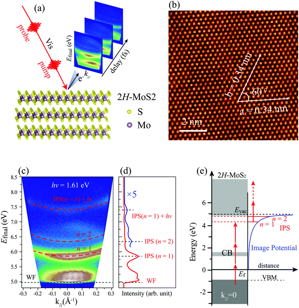 | ||
| Fig. 1 (a) Schematic drawing to show the measurements of TR-MR-mPPE spectra for the bulk 2H-MoS2 surface using the pump–probe method. (b) An STM image of the MoS2 surface acquired at a sample bias of 1.0 V and the tunneling current of 140 pA. (c) Typical mPPE spectrum of 2H-MoS2 surface measured using photon energy of 1.61 eV at zero pump–probe delay time. The dashed red lines are the fitting curves of the parabolic dispersed bands. (d) Integrated signals of near k‖ = 0 within Δk‖ = ±0.03 Å−1. The blue line is a magnified segment at high-energy final states. The peak positions are labeled by WF (work function of MoS2), Rydberg-like series n = 1, 2 (IPS), and IPS (n = 1) + hν. (e) Energy diagram to show the mPPE processes through the intermediate IPSs. | ||
Fig. 1(c) shows a typical energy-momentum (E–k‖) map of the band structure measured at an excitation photon energy of 1.61 eV at zero pump–probe delay time. The final-state (Efinal) energies recorded by the analyzer are referenced with respect to the Fermi energy (Ef = 0). Fig. 1(d) is the integrated line trace at k‖ = 0. The low-energy cutoff corresponds to the vacuum level (Evac) through the mPPE process, which determines the work function (Φ) of the bulk 2H-MoS2 surface by Φ = Evac − Ef = 4.98 eV.46 Three upward-dispersed bands are observed, which can be well fitted with the parabolic line shape (overlaid dashed red lines), with an approximate effective mass of m* ≈ me, where me is the rest mass of the electron. On the basis of the parabolic dispersion of these bands in accordance with the band dispersion of IPSs, we tentatively attribute them to IPS (n = 1), IPS (n = 2), and IPS-related state (IPS (n = 1) + hν). Fig. 1(e) shows the energy diagram extracted from the experimental observations, where the horizontal red lines below the Evac correspond to the IPS series n = 1 and 2, respectively.
To confirm our assignments, we performed a series of mPPE measurements by varying the excitation photon energy from 1.57 eV to 1.72 eV recorded at zero delay time (Fig. S1, ESI†). The corresponding line traces integrated near k‖ = 0 from each mPPE spectrum in Fig. S1 (ESI†) are plotted as a function of photon energy in Fig. 2(a). The extracted peak positions of IPS (n = 1) and IPS (n = 2) in the final-state energies are then plotted as a function of excitation photon energy in Fig. 2(b), which present explicit linear dependence. The slopes by linear fitting of the data in IPS (n = 1) and IPS (n = 2) are both around 1, which indicates that in both cases the emission takes place by absorbing one photon, while the multi-photonic order for both states is 4.47 Therefore, the energy positions of IPS (n = 1) and IPS (n = 2) at k‖ = 0 can be obtained by En = Efinal − hν. The observed energy difference between IPS (n = 1) and IPS (n = 2) is ∼0.56 eV. The high-energy state of IPS (n = 1) + hν can be assigned to the replica of IPS (n = 1) in above-threshold photoemission (ATP).21,48 The extracted values of (En − Ef), (Evac − En), and m* are summarized in Table 1. We also measured the distance-voltage (z-V) curves and dz/dV curves at different constant-current setpoints. As shown in Fig. S3 (ESI†), a series of setpoint-current-dependent steps or peaks are observed in the z-V or dz/dV curves. The peak labeled by n = 1 positioned below the Evac by about 0.5–0.6 eV should correspond to the IPS (n = 1) in the mPPE measurements, where their energy difference can be ascribed to the Stark shift in the STM measurements.49 Hence, the existence of the IPSs can also be supported.
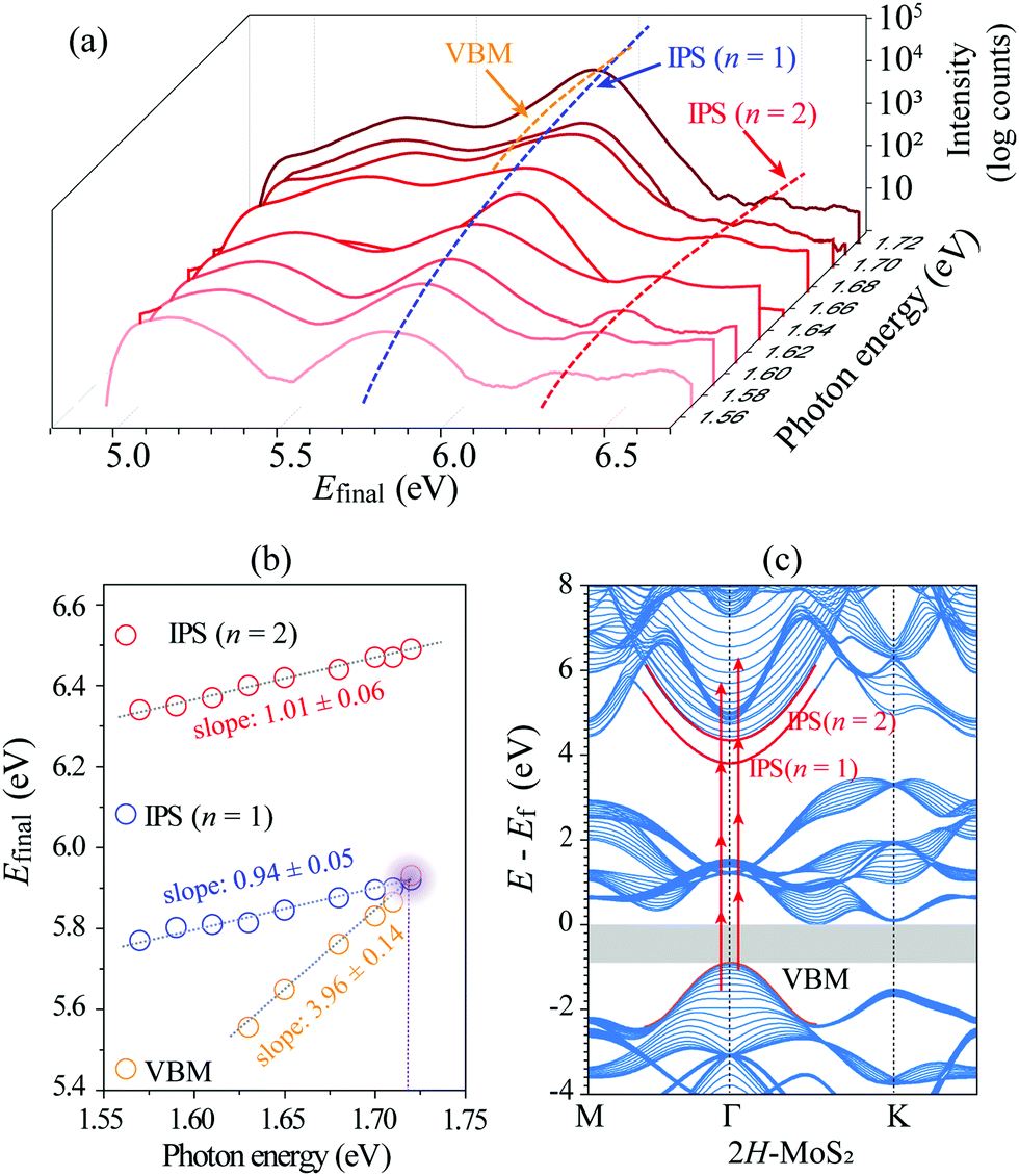 | ||
| Fig. 2 (a) Plot of integrated signals at k‖ = 0 against photon energy and the final-state energy using a p-polarized light. (b) Peak positions in the final-state energies against photon energies. The dotted lines represent linear fitting of the data of IPS (n = 1) and IPS (n = 2), respectively. (c) Calculated band structure along M–Γ–K for the 2H-MoS2 surface. The two upward dispersed red parabolic curves denote the IPS (n = 1) and IPS (n = 2) band, and the lower downward parabolic curve denotes the valence band maximum (VBM). The arrowed red segments indicate photoemission transitions via the IPSs. | ||
| E n –Ef (eV) | E vac–En (eV) | m*/me | ||
|---|---|---|---|---|
| TR-mPPE | IPS (n = 1) | 4.21 ± 0.04 | 0.77 ± 0.02 | 1.05 ± 0.06 |
| IPS (n = 2) | 4.77 ± 0.02 | 0.21 ± 0.02 | 0.99 ± 0.06 | |
| Hydrogenic model | IPS (n = 1) | 0.66 | ||
| IPS (n = 2) | 0.16 | |||
| DFT | IPS (n = 1) | 0.57 | 0.9 | |
| IPS (n = 2) | 0.02 | 1.0 |
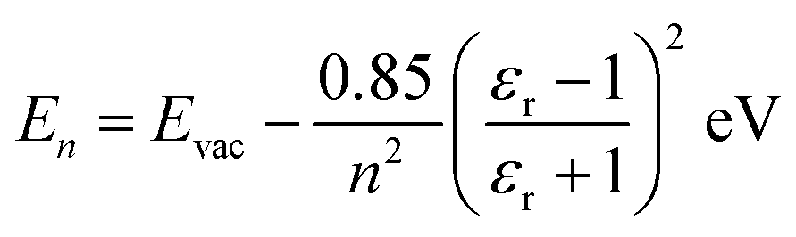
On semiconducting surfaces, the IPS binding energy, namely, energy relative to Evac can be estimated using a classical Rydberg-like series:3,17,50
 | (1) |
We also performed theoretical calculations on the band structure of the bulk 2H-MoS2 based on DFT. Fig. 2(c) shows the projected band structure of 2H-MoS2 at the M–Γ–K plane calculated using a slab model consisting of a 5-layer MoS2 using a tight-binding (TB) approach. It was observed that the calculated band structure in the VB is in good agreement with the experimentally measured band structure using the ARPES (Fig. S2, ESI†). The DFT-PBE band gap of 2H-MoS2 indicated by the grey area is ∼1.0 eV, which is smaller than the experimental value.32,55 This is owing to the well-known self-interaction error in DFT, which will underestimate the band gap. The simulated IPS (n = 1) and IPS (n = 2) are marked in red, whose features well reproduce the experimental observations. The arrowed 4-segment lines indicate 4PPE processes from the initial VB states via the intermediate IPSs. As our experimental observations indicate since the initial states are both located in the VB, the intermediate IPSs could be sufficiently populated by the pump light, and thus produce the much strong 4PPE signals by the probe light.
Based on DFT calculations, the binding energies for IPS (n = 1) and IPS (n = 2) are 0.57 and 0.02 eV, respectively. It is lower than the experimental value because the DFT calculations cannot reproduce the long-range Coulomb potential correctly.19 However, the DFT calculations successfully reproduce the NFE character of the IPSs. The fitted effective masses of these two IPSs are close to 1.0 as shown in Table 1.
Fig. 3 shows an MR-mPPE image with a wide k‖ range for the resonance between the valence band maximum (VBM) and IPS. It is noticed that the fitting lines of the data for VBM and IPS (n = 1) across at the photon energy of about 1.72 eV, as shown in Fig. 2(b), indicate the existence of resonance between the states. Actually, such resonance should also be k‖-momentum-dependent, as schematically shown in Fig. 3(a). Due to the upward dispersion of the IPSs and the downward dispersion of the VBM, the resonance may also exist between different mth excitations. As shown in Fig. 3(b), the relatively strong signals show resonance between the IPS (n = 1) and the VBM in the 4PPE processes at k‖= 0. Moreover, as indicated by the yellow arrows, the resonance may appear between 4th IPS (n = 1) and 5th VBM at larger k‖-momenta. More related MR-mPPE images using 1.68 and 1.63 eV excitation photon energy are also shown in Fig. 3(c) and (d), respectively. We expect that such enhanced signals at the band crossing could be a general property of IP states in the spectroscopy of semiconductors.
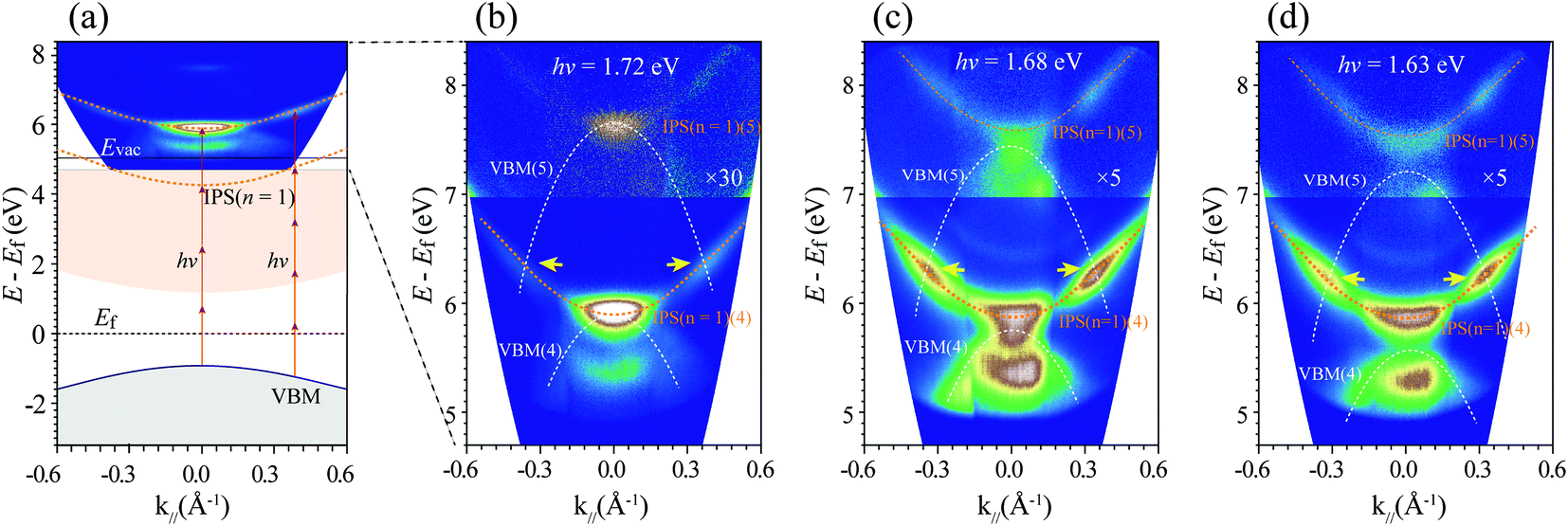 | ||
| Fig. 3 (a) Schematic drawing showing the existence of resonance between the VBM and IPS (n = 1) in the final states. The experimentally measured E(k‖)-resolved mPPE spectra are overlaid in the top panel. A k‖-momentum-dependent processes of 4PPE (k‖ = 0) and 5PPE (k‖ ≈ 0.40 Å−1) are indicated by the arrowed red lines. (b) E(k‖)-dependent MR-mPPE spectra showing the resonance between the replicas of the VBM and IPS (n = 1) in the 4th and 5th order excitations, marked by the bracket numbers (4) and (5). The intensity of spectra in the upper part is magnified by a factor of 30. The crossing of the bands gives relatively strong signals, indicating their resonances at the band crosses. (c) MR-mPPE spectra with a wide k‖ range measured at the near-resonance photon energy of 1.68 eV and (d) the off-resonance photon energy of 1.63 eV, respectively. Note that in (b) a much shorter acquisition time was used due to the strong resonance signals. | ||
To investigate the role of the electron transition and relaxation process between IPS and VBM, a pulsed laser of 355 nm was used as the excitation source. We image the photoelectron distributions as a function of delay time τ between pump–probe pulses and record the coherent polarization dynamics in Fig. 4(a). The interferograms for k‖ = 0 in Fig. 4(a) and photoelectron distribution for τ = 0 in Fig. 4(b) represent cross-sections through the three-dimensional (E, k, τ) data. The distinct polarization dynamics of the IPS (n = 1) are evident in the correlation trace representing cross-sections through the interferogram for the Efinal marked by the red line cutting in Fig. 4(a).
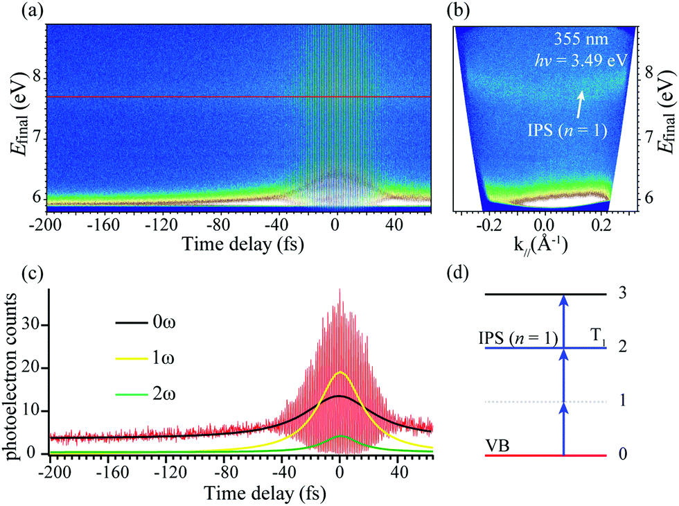 | ||
| Fig. 4 3D photoemission spectra for image potential states with 3.49 eV excitation photon energy. (a) Interferogram of the photoelectron counts vs. Efinal and scanned pump–probe time delay τ at k‖ = 0. (b) ARPES image for a pump–probe delay τ = 0. (c) Correlation measurement was obtained by taking cross-sections through the interferogram in (a) at Efinal for the IPS (n = 1). Oscillations with approximately the period of the carrier wave (∼1.18 fs) represent interference between the pump and probe pulse-induced polarizations excited in the sample. (d) The energy diagram of the expected 3PPE processes in (b) from VB to IPS. | ||
In order to show more clearly the coherence dynamics in the 3PP process, the interferogram shown in Fig. 4(c) is Fourier transformed with respect to time to generate the components at dc (0ω), the first (1ω), and the second (2ω) harmonics of the driving field. The 0ω component has contributions from the incoherent hot electron population dynamics, whereas the 1ω and 2ω components characterize the linear and second-order nonlinear coherences.41 From the cross-section of IPS at Efinal = 7.7 eV shown in Fig. 4(a), the obtained interferometric two-pulse correlation trace of Fig. 4(c) is modeled with an optical Bloch equation (OBE) approach56,57 for a four-level scheme in Fig. 4(d). The simulation gives a population lifetime of T1 = 33 fs for IPS (n = 1), showing an ultrafast manner. This value is comparable to the pulse duration of ∼30 fs. We adopt an estimated error of ±5 fs for T1 owing to the fact that the OBE is a crude model for the bulk sample.57
The photoexcited electron on IPS can be scattered to other bulk states through electron–phonon interactions. In this case, the lifetime of IPS is normally strongly affected by its overlap with the bulk states and the electron–phonon interaction. The lifetime measured in this report is in the same magnitude compared with other metal or semiconducting surfaces, suggesting the electronic properties of IPSs on different surfaces exhibit general character. The electron–phonon interaction of IPSs are proposed to be small.25 However, the diffuse character of IPS may lead to a large orbital overlap with the bulk states, resulting in a short lifetime.
The lifetime of IPS (n = 1) on MoS2 is slightly shorter than that on Cu(100) (40 fs) and Ag(100) (55 fs) surfaces.58 On Cu(100) and Ag(100) surfaces, the IPS is located at about midgap in the projected band structure and has a small overlap with bulk states, resulting in a relatively long lifetime. In contrast, the IPS of 2H-MoS2 is located close to the unoccupied states along Γ–K, as shown in the calculated band structure in Fig. 2(c). Such energy level alignment is similar to the Cu(111) surface, where its IPS (n = 1) has a lifetime of about 20 fs.59
The IPSs on MoS2 are found to have high energy relative to the Ef with a short lifetime with tens of fs, which makes it difficult for IPS to be applied in charge transport. However, we propose that there might be different techniques, which can reduce the energy of IPS and elongate their lifetime. For example, the cation or anion doping may induce dipole moment perpendicular to the surface, which may reduce the energy of IPS. If 2D MoS2 can be wrapped into a 1D nanotube, the 1D NFE state can be formed and the structure distortion may result in a dipole moment which can stabilize the 1D NFE conduction channel. It will need further experimental and theoretical investigations.
4. Conclusion
We have measured the electronic structure and ultrafast dynamics of IPSs at the 2H-MoS2 surface using the TR-MR-mPPE technique. The parabolic dispersion of the observed bands, with their energy minima located at 0.77 and 0.21 eV below the Evac, can be assigned to the IPS (n = 1) and (n = 2), respectively, which can be well described by the classical hydrogenic model and have been supported by our DFT calculations. The effective masses of the IPSs are close to the rest mass of the free electron, clearly presenting the NFE character. These results also suggest a good screening effect of the excited states on the MoS2 surface. Owing to the downward and upward dispersion of VBM and IPSs, we also observed the k‖-momentum-dependent resonances between replicas of VBM and IPS (n = 1) in mPPE spectra. The relaxation of the photoexcited electrons at the IPS (n = 1) shows an ultrafast manner, in a time scale of about 33 fs. We propose the existence of IPSs, as well as their NFE character and short lifetime, can provide useful information for understanding the electron dynamics in other TMD materials.Conflicts of interest
There are no conflicts to declare.Acknowledgements
This work was financially supported by the National Key R&D Program of China (Grant No. 2016YFA0200603 and 2017YFA0205004), the Anhui Initiative in Quantum Information Technologies (AHY090000), the Strategic Priority Research Program of Chinese Academy of Sciences (XDB36020200), the Fundamental Research Funds for the Central Science Advances Universities (No. WK2340000088), and the National Natural Science Foundation of China (11620101003, 11904349, 21972129).References
- K. Giesen, F. Hage, F. J. Himpsel, H. J. Riess and W. Steinmann, Phys. Rev. Lett., 1985, 55, 300–303 CrossRef CAS PubMed.
- M. Kutschera, M. Weinelt, M. Rohlfing and T. Fauster, Appl. Phys. A: Mater. Sci. Process., 2007, 88, 519–526 CrossRef CAS.
- K. Gillmeister, M. Kiel and W. Widdra, Phys. Rev. B: Condens. Matter Mater. Phys., 2018, 97, 085424 CrossRef CAS.
- A. D. Miller, I. Bezel, K. J. Gaffney, S. Garrett-Roe, S. H. Liu, P. Szymanski and C. B. Harris, Science, 2002, 297, 1163–1166 CrossRef CAS PubMed.
- J. Zhao, N. Pontius, A. Winkelmann, V. Sametoglu, A. Kubo, A. G. Borisov, D. Sánchez-Portal, V. M. Silkin, E. V. Chulkov, P. M. Echenique and H. Petek, Phys. Rev. B: Condens. Matter Mater. Phys., 2008, 78, 085419 CrossRef.
- M. C. Galbraith, M. Marks, R. Tonner and U. Höfer, J. Phys. Chem. Lett., 2014, 5, 50–55 CrossRef CAS PubMed.
- J. Zhao, M. Feng, D. B. Dougherty, H. Sun and H. Petek, ACS Nano, 2014, 8, 10988–10997 CrossRef CAS PubMed.
- G. Dutton and X. Y. Zhu, J. Phys. Chem. B, 2002, 106, 5975–5981 CrossRef CAS.
- S. Tan, A. Argondizzo, J. Ren, L. Liu, J. Zhao and H. Petek, Nat. Photonics, 2017, 11, 806–812 CrossRef CAS.
- M. V. Mamonova, V. V. Prudnikov and I. A. Prudnikova, Surface physics: theoretical models and experimental methods, CRC Press, 2016 Search PubMed.
- S. Tognolini, S. Ponzoni, F. Sedona, M. Sambi and S. Pagliara, J. Phys. Chem. Lett., 2015, 6, 3632–3638 CrossRef CAS PubMed.
- X. Cui, C. Wang, A. Argondizzo, S. Garrett-Roe, B. Gumhalter and H. Petek, Nat. Phys., 2014, 10, 505–509 Search PubMed.
- X. Y. Zhu, J. Phys. Chem. B, 2004, 108, 8778–8793 CrossRef CAS.
- K. F. Mak, K. He, J. Shan and T. F. Heinz, Nat. Nanotechnol., 2012, 7, 494–498 CrossRef CAS PubMed.
- O. V. Yazyev and A. Kis, Mater. Today, 2015, 18, 20–30 CrossRef CAS.
- P. M. Echenique and J. B. Pendry, Prog. Surf. Sci., 1989, 32, 111–172 CrossRef CAS.
- P. M. Echenique and M. E. Uranga, Surf. Sci., 1991, 247, 125–132 CrossRef CAS.
- U. Höfer, I. L. Shumay, C. Reuß, U. Thomann, W. Wallauer and T. Fauster, Science, 1997, 277, 1480–1482 CrossRef.
- V. M. Silkin, J. Zhao, F. Guinea, E. V. Chulkov, P. M. Echenique and H. Petek, Phys. Rev. B: Condens. Matter Mater. Phys., 2009, 80, 121408 CrossRef.
- N. Armbrust, J. Güdde and U. Höfer, New J. Phys., 2015, 17, 103043 CrossRef.
- D. Gugel, D. Niesner, C. Eickhoff, S. Wagner, M. Weinelt and T. Fauster, 2D Mater., 2015, 2, 045001 CrossRef.
- M. Feng, J. Zhao and H. Petek, Science, 2008, 320, 359–362 CrossRef CAS PubMed.
- J. Zhao, M. Feng, J. Yang and H. Petek, ACS Nano, 2009, 3, 853–864 CrossRef CAS PubMed.
- S. Hu, J. Zhao, Y. Jin, J. Yang, H. Petek and J. G. Hou, Nano Lett., 2010, 10, 4830–4838 CrossRef CAS PubMed.
- J. Zhao and H. Petek, Phys. Rev. B: Condens. Matter Mater. Phys., 2014, 90, 075412 CrossRef CAS.
- R. Yamamoto, T. Yamada, M. Taguchi, K. Miyakubo, H. S. Kato and T. Munakata, Phys. Chem. Chem. Phys., 2012, 14, 9601–9605 RSC.
- B. Borca, C. Castenmiller, M. Tsvetanova, K. Sotthewes, A. N. Rudenko and H. J. W. Zandvliet, 2D Mater., 2020, 7, 035021 CrossRef CAS.
- T. Cao, G. Wang, W. Han, H. Ye, C. Zhu, J. Shi, Q. Niu, P. Tan, E. Wang, B. Liu and J. Feng, Nat. Commun., 2012, 3, 887 CrossRef PubMed.
- B. Radisavljevic and A. Kis, Nat. Mater., 2013, 12, 815–820 CrossRef CAS PubMed.
- J. Madeo, M. K. L. Man, C. Sahoo, M. Campbell, V. Pareek, E. L. Wong, A. Al-Mahboob, N. S. Chan, A. Karmakar, B. M. K. Mariserla, X. Li, T. F. Heinz, T. Cao and K. M. Dani, Science, 2020, 370, 1199–1203 CrossRef CAS PubMed.
- A. Tanaka, N. J. Watkins and Y. Gao, Phys. Rev. B: Condens. Matter Mater. Phys., 2003, 67, 113315 CrossRef.
- S. K. Mahatha, K. D. Patel and K. S. R. Menon, J. Phys.: Condens. Matter, 2012, 24, 475504 CrossRef CAS PubMed.
- P. Hein, A. Stange, K. Hanff, L. X. Yang, G. Rohde, K. Rossnagel and M. Bauer, Phys. Rev. B: Condens. Matter Mater. Phys., 2016, 94, 205406 CrossRef.
- R. Wallauer, J. Reimann, N. Armbrust, J. Güdde and U. Höfer, Appl. Phys. Lett., 2016, 109, 162102 CrossRef.
- R. Wallauer, P. Marauhn, J. Reimann, S. Zoerb, F. Kraus, J. Güdde, M. Rohlfing and U. Höfer, Phys. Rev. B: Condens. Matter Mater. Phys., 2020, 102, 125417 CrossRef CAS.
- K. F. Mak, C. Lee, J. Hone, J. Shan and T. F. Heinz, Phys. Rev. Lett., 2010, 105, 136805 CrossRef PubMed.
- M. Palummo, M. Bernardi and J. C. Grossman, Nano Lett., 2015, 15, 2794–2800 CrossRef CAS PubMed.
- F. Liu, M. E. Ziffer, K. R. Hansen, J. Wang and X. Zhu, Phys. Rev. Lett., 2019, 122, 246803 CrossRef CAS PubMed.
- M. Reutzel, A. D. Li and H. Petek, Phys. Rev. X, 2019, 9, 011044 CAS.
- H. Petek and S. Ogawa, Prog. Surf. Sci., 1997, 56, 239–310 CrossRef CAS.
- G. Kresse and J. Furthmüller, Phys. Rev. B: Condens. Matter Mater. Phys., 1996, 54, 11169–11186 CrossRef CAS PubMed.
- J. P. Perdew, K. Burke and M. Ernzerhof, Phys. Rev. Lett., 1997, 78, 1396 CrossRef CAS.
- S. Grimme, J. Antony, S. Ehrlich and H. Krieg, J. Chem. Phys., 2010, 132, 154104 CrossRef PubMed.
- R. Addou, L. Colombo and R. M. Wallace, ACS Appl. Mater. Interfaces, 2015, 7, 11921–11929 CrossRef CAS PubMed.
- H. Xu, D. Han, Y. Bao, F. Cheng, Z. Ding, S. J. R. Tan and K. P. Loh, Nano Lett., 2018, 18, 5085–5090 CrossRef CAS PubMed.
- J. Lin, J. Zhong, S. Zhong, H. Li, H. Zhang and W. Chen, Appl. Phys. Lett., 2013, 103, 063109 CrossRef.
- S. Tognolini, S. Achilli, L. Longetti, E. Fava, C. Mariani, M. I. Trioni and S. Pagliara, Phys. Rev. Lett., 2015, 115, 046801 CrossRef CAS PubMed.
- M. Reutzel, A. Li and H. Petek, Phys. Rev. B: Condens. Matter Mater. Phys., 2020, 101, 011044 CrossRef.
- D. B. Dougherty, P. Maksymovych, J. Lee, M. Feng, H. Petek and J. T. Yates, Phys. Rev. B: Condens. Matter Mater. Phys., 2007, 76, 3398–3407 CrossRef.
- M. Muntwiler and X. Y. Zhu, New J. Phys., 2008, 10, 113018 CrossRef.
- Y. Li, A. Chernikov, X. Zhang, A. Rigosi, H. M. Hill, A. M. van der Zande, D. A. Chenet, E.-M. Shih, J. Hone and T. F. Heinz, Phys. Rev. B: Condens. Matter Mater. Phys., 2014, 90, 205422 CrossRef.
- A. Molina-Sánchez and L. Wirtz, Phys. Rev. B: Condens. Matter Mater. Phys., 2011, 84, 155413 CrossRef.
- T. Cheiwchanchamnangij and W. R. L. Lambrecht, Phys. Rev. B: Condens. Matter Mater. Phys., 2012, 85, 205302 CrossRef.
- E. V. Chulkov, V. M. Silkin and P. M. Echenique, Surf. Sci., 1999, 437, 330–352 CrossRef CAS.
- M. M. Ugeda, A. J. Bradley, S.-F. Shi, F. H. da Jornada, Y. Zhang, D. Y. Qiu, W. Ruan, S.-K. Mo, Z. Hussain, Z.-X. Shen, F. Wang, S. G. Louie and M. F. Crommie, Nat. Mater., 2014, 13, 1091–1095 CrossRef CAS PubMed.
- W. Nessler, S. Ogawa, H. Nagano, H. Petek, J. Shimoyama, Y. Nakayama and K. Kishio, Phys. Rev. Lett., 1998, 81, 4480–4483 CrossRef CAS.
- S. Tan, Y. Dai, S. Zhang, L. Liu, J. Zhao and H. Petek, Phys. Rev. Lett., 2018, 120, 126801 CrossRef CAS PubMed.
- I. L. Shumay, U. Höfer, C. Reuß, U. Thomann, W. Wallauer and T. Fauster, Phys. Rev. B: Condens. Matter Mater. Phys., 1998, 58, 13974–13981 CrossRef CAS.
- K. Schubert, A. Damm, S. V. Eremeev, M. Marks, M. Shibuta, W. Berthold, J. Güdde, A. G. Borisov, S. S. Tsirkin, E. V. Chulkov and U. Höfer, Phys. Rev. B: Condens. Matter Mater. Phys., 2012, 85, 205431 CrossRef.
Footnote |
| † Electronic supplementary information (ESI) available. See DOI: 10.1039/d1cp03527d |
| This journal is © the Owner Societies 2021 |