
 Open Access Article
 This Open Access Article is licensed under a
 Creative Commons Attribution 3.0 Unported Licence
Bismuth selenide topological insulator materials for green energy devices: prospects and applications
Razieh Khaki
 ,
Mahmood Moradi
*,
Gholam Hossein Bordbar
,
Hana Kazemi
,
Saeid Davatolhagh
and
Meysam Pazoki
*
,
Mahmood Moradi
*,
Gholam Hossein Bordbar
,
Hana Kazemi
,
Saeid Davatolhagh
and
Meysam Pazoki
*
Department of Physics, College of Sciences, Shiraz University, Shiraz 71946-84795, Iran. E-mail: mmoradi@shirazu.ac.ir
First published on 4th December 2025
Abstract
Bismuth selenide topological insulator material has emerged as a prototype three-dimensional topological insulator and has been the center of attention for a new generation of related devices. Theoretical and experimental characterization of the underlying physical phenomena, together with proper evaluation of the current picture, is essential to envision, design, and engineer Bi2Se3 for the realization of important device applications. Furthermore, the presented characterization methodologies can be adopted for similar three-dimensional topological insulator counterpart materials, such as bismuth telluride and antimony selenide. Herein, we summarize recent research advancements on bismuth selenide, both theoretically and experimentally, and provide a perspective for future applications in spintronic and quantum computing devices as well as other green-energy-based scientific endeavors. Different synthesis methods, physical properties, the occurrence of quantum mechanical phenomena and their methods of calculation, device applications and characterization methods that have been implemented for bismuth selenide are classified and comprehensively reviewed. Future prospects addressing the challenges and opportunities are also highlighted.
 Razieh Khaki | Razieh Khaki, born 1988, is a PhD student and researcher in the School of Science, Physics Division, at Shiraz University. She has an MSc in solid state physics from Shiraz University. Her expertise includes dye-sensitized solar cells, synthesis of novel nanostructures and topological insulators, fabrication and characterization of semiconductor devices such as infrared photodetectors for green energy applications, as well as related DFT calculations and modelling. |
 Mahmood Moradi | Mahmood Moradi, a full professor in condensed matter physics, holds a senior professorship position at Shiraz University. He received his PhD from Kent University at Canterbury, England, in 1989. His research focuses on classical and quantum density functional theory and their numerical calculations, as well as experimental research on semiconductor devices, nanostructures, such as the fabrication of nanotubes, nanorods, thin films, and a new generation of solar cells (including perovskites). He also conducted experimental work on electromagnetic absorption He has supervised more than 200 postgraduate students and he is a co-author of more than 128 publications. |
 Gholam Hossein Bordbar | Gholam Hossein Bordbar, born in 1967, is a full professor in theoretical physics, holds a professorship position at Shiraz University. He received his PhD from Amirkabir University of Technology in 1997. His research focuses on interacting quantum many-particle systems, quantum many-body methods, low dimensional systems and quantum fluids in various fields of physics. He has supervised several post-graduate students and post-doctoral researchers, and he is a co-author of more than 115 publications in various academic journals. |
 Hana Kazemi | Hana Kazemi, is a researcher in the Department of Solid-State Physics at Shiraz University. She earned her PhD from Shiraz University and her MSc from Shahid Beheshti University. She is skilled in various technical areas, including nanoparticle synthesis, thin-film deposition, and characterization techniques. Her research focuses on the fabrication of nanostructures and thin films, particularly nanomagnetic materials and 2D materials, with applications in electromagnetic wave absorption, photocatalysis, and semiconductor devices. |
 Saeid Davatolhagh | Saeid Davatolhagh is a professor in the condensed-matter and complex systems group at the physics department of Shiraz University. He obtained his PhD in condensed-matter physics from The Ohio State University at Columbus, USA, in 2001. His research interest mainly includes the computational study of both the classical and quantum phases of condensed matter. For the past ten years, his research group has been focused on ab initio discovery and characterization of topological quantum matter employing DFT-based computational methods, which has led to the identification of a particularly interesting Chern insulator state with maximum d-shell magnetic moment and high Curie temperature in a class of d0–d compounds with half-Heusler crystal structure. |
 Meysam Pazoki | Meysam Pazoki, born in 1984, is an associate professor and researcher with the Department of Solid-State Physics, Shiraz University. Dr Pazoki received his docent degree in solid-state physics from Uppsala University in 2019. His areas of interest include (T)DFT calculation of semiconductors for photovoltaic devices and CO2 reduction applications, dye-sensitized and perovskite solar cells, UV photodetectors, as well as device characterization methods, including impedance spectroscopy, electrochemical methods, and small photovoltage/current transients, and material characterization methods such as laser spectroscopy and Stark spectroscopy. |
1. Introduction
Emerging materials pave the way for the advancement of health and wealth in our lives, wherein new resources are needed based on our demands. Nanostructured functional materials and topological insulators are examples of materials where one can engineer the properties to achieve specific potential capabilities that had not previously been possible. Recently emerging topological insulator material families have shown quantum phenomena such as spin-polarized sensing and quantum spin Hall effect, anomalous Hall effect and Majorana fermions, along with their special optoelectronic properties, making them candidates for near-future quantum computing, sensing, detecting and other device applications. To develop related technologies, extend and engineer the material properties and design efficient new devices, one needs to deeply lucubrate the fundamentals of topological insulator physical properties with the help of quantum calculations and experimental material/device characterization techniques. Bismuth selenide is an important example of a prototype of the three-dimensional topological insulator family, which is the most extensively investigated so far, and is the topic of the present article. Mazumder and Wang, in separate review articles,1,2 investigated and collected data from the recent experimental efforts considering bismuth selenide, material synthesis and applications. However, the aim of the current manuscript is to present an extensive perspective review, wherein one can find the theoretical basis and the connections to experiment, quantum calculations and experimental device characterizations, together with the above-mentioned aspects, which are still missing. Herein, we aim to present such a picture. In Section 2, an introduction to bismuth selenide will be presented. Section 3 investigates the quantum mechanical phenomena and fundamentally interesting experiments related to future quantum computing and spintronics. Section 4 is devoted to density functional theory (DFT) calculations and understanding the experimental data from ab initio calculations. Material synthesis, characterization methods, device applications and their drawbacks and benefits are presented in Sections 5–7, respectively. The final comments and concluding remarks come at the end in Section 8. Scheme 1 shows a schematic summary of the scientific questions posed and discussed herein, based on the current research status, presenting an overview of the work. | ||
| Scheme 1 A summary of the outline and aims of the current work. | ||
2. Bismuth selenide
Bismuth selenide is a semiconductor with a bandgap of 0.3 eV that is known as a prototype 3-dimensional topological insulator. It has been the centre of attention for quantum mechanical studies of topological insulators for many years and is the most extensively investigated to date. Here, selenium vacancies are thermodynamically favourable during growth, which makes it an n-type semiconductor with an excess of electron charge carriers. The bulk electronic structure shows insulating behaviour with a narrow band gap and topologically protected surface states (a Dirac cone within the bandgap electronic structure) exhibiting metallic behaviour. Although it was theoretically predicted earlier, experimental observation of this Dirac cone in an electronic structure was evidenced in 2009.3 Since then, evidence for many quantum mechanical phenomena, such as the quantum spin Hall effect, quantum anomalous Hall effect, Majorana fermions, and spin-momentum locking, has been reported. As a consequence, the recent ongoing research continues in efforts to advance spintronic and quantum computing devices.3D topological insulators are very decent thermoelectric materials, and the first studies on bismuth selenide and its alloy with its counterpart bismuth telluride, Bi2Te3,4 were devoted to thermoelectric applications. Therefore, different synthesis approaches for single crystals, bulk, and nanostructures have been pursued (Section 5), and, at the same time, material characterization (Section 6) studies on Bi2Se3 have helped to accomplish device fabrication and provide theoretical explanations.
The spectacular physical properties of bismuth selenide lead to diverse capabilities in different green energy applications, in medicine, engineering, and basic science, and in the direction of sustainable development goals outlined by the United Nations for the human future. Many theoretical calculations, experimental characterizations, device fabrications, and joint theoretical–experimental research studies have been devoted to bismuth selenide materials, and preparation of the groundwork is still ongoing. For example, one very interesting and fundamental topic is Majorana fermions, which are the basis of quantum bits for future quantum computing advances. Moreover, in order to make use of the topologically protected surface states, one can reduce the bulk contribution in the electronic states by reducing the bulk carriers by doping or having smaller structures with high surface-to-volume ratios. Table 1 presents a summary of selected physical properties of bismuth selenide. Inspired by this, in this article, we aim to probe theoretical and experimental explorations and relate them in a joint theoretical–experimental approach so that we can draw a picture of the current status and discuss the prospects for future potential studies.
| Property | Value/status | Ref. |
|---|---|---|
| Appearance | Gray-light dark | 2 |
| Melting/boiling point | 710/2360 °C | 2 |
| Density | 6.82 g cm−1 | 2 |
| Solubility | Insoluble in water and week acids | |
| Toxicity | A level of toxicity for human and marine life | |
| Crystal structure at room temperature | R![[3 with combining macron]](https://www.rsc.org/images/entities/char_0033_0304.gif) m rhombohedral space group 166 m rhombohedral space group 166 |
5 |
| Thermal conductivity at room temperature | 1 W m−1 K−1 | 6 |
| Refractive index | 3.88 | 7 |
| Hall coefficient | 0.14 × 10⁻⁶ Ω m tesla−1 | 8 |
| Electron effective mass | 0.13m0 | 9 |
| Dielectric constant | 29.8 | 10 |
| Plasma frequency ωp | 1.36 × 10⁻¹⁴ s−1 | 10 |
| Semiconducting state | n-Type with inherent selenium vacancies | |
| Bulk-band gap | 300 meV | |
| Doping state | Cu, Sb, Ca, Cd, Pb, Zn, Fe, Cr, In, Mn, Ni … | 10–15 |
| Carrier density-nanostructured | 1017–1019 cm−3 | |
| Absorption coefficient | 4.4 × 105 cm−1 | 7 |
| Ionization energy | 4.45 eV | 16 |
| Electron–hole lifetime at 300 K | 50 ps | 17 |
| Surface states density | 4 × 1013 cm−2 | 1 |
| Superconducting state | Superconductor at 3.8 K, Cu doping | 18 |
| Hall resistivity | 4 mΩ cm | 19 |
| Mobility | 500–700 cm2 V−1 S−1 | 20 |
| Thermoelectric properties, typical values at room temperature | ||
| a. Figure of merit | a. 0.01 | 21 |
| b. Seebeck coefficient | b. 1.15 × 10⁻⁴ V K−1 | |
| c. Thermal conductivity | c. 0.75 W m−1 K−1 |
For many of the reported green energy devices, the interaction of light and matter and its photo-physics plays the key role; moreover, the concepts can be extended to a wide range of possible technological implications, as well as similar topological insulator materials. The bulk and surface broadband optical properties of bismuth chalcogenides have been widely investigated via different characterization methods (Section 6), and the corresponding details and values are reported, for example, for refractive index and absorption spectra, in the literature.22–25 For bulk Bi2Se3, the main optical transitions happen between the selenium 4p states and the hybridized Se(4p)–Bi(6p) states at the valence/conduction band edges. However, promising optical properties stem from the surface electronic structure, which is related to the preservation of time-reversal symmetry in 3D topological insulators, the spin-momentum lock, spin–orbit coupling effects, together with massless electrons in the Dirac cone. Such effects enable novel potential applications to be quantum mechanically possible, i.e., helicity-preserving PL26 with chiral spin-momentum textures and polarizability-dependent photocurrent.27
The detection of incoming light polarization for infrared light at very low temperatures has been reported for Bi2Se3-based photo-detectors (see ref. 27 Fig. 3) as a phenomenon that is not plausible in typical infrared detectors. Bismuth selenide's unconventional room temperature photoluminescence in the range 1.8–2.4 eV has yet to be evidenced and is attributed to confined surface excitons. Kung et al. observed that the polarization preservation for the electronic transition between the Bi2Se3 surface states is related to chiral excitons.26 They found that polarization of chiral exciton PL is preserved up to room temperature, and is robust with respect to chemical substitutions. This can be attributed to the weakness of spin–flip scattering between surface states with opposite helicity. A theoretical model was proposed to explain the PL transition from the surface states,26 which can quantitatively describe the observed polarizability preservation in experiments. The transition between the surface state 2 (SS2) and Rashba surface state (RSS) is the main responsible transition. The weak charge carrier interactions with phononic modes in this region allow radiative decay of the exciton states, resulting in the observed unconventional PL.
The corresponding PL yield can be further enhanced via decoration with gold nanoparticles, which enables localised surface plasmon resonance to exist.28 The Bi2Se3/Au system shows a modified PL peak/intensity and is related to hybridization of gold–Se/Bi orbitals, accompanied by a charge transfer from Au to bismuth selenide with an appreciably enhanced PL. New recombination channels are thus created, leading to retarded recombination pathways and enhanced PL with circular polarizability,28 which can be explained via a mechanism called exciton–plasmon coupling.
The chemical bonding effects in bismuth chalcogenides and the selenium bismuth lattice25,29–32 are, on the other hand, responsible for the mentioned physical properties and the related device implications; therefore, exploring the chemistry of the selenium–bismuth bonds within the bulk or at the surface is of fundamental importance for any green energy application. Here, the light absorption and the subsequent charge excitations happen mainly between the valence band selenium 4p states and the hybridized Se(4p)–Bi(6p) states in the conduction band. The local distribution of the charge density within the chemical bond is different among the selenium atoms that are bonded with one or two Bi atom(s), corresponding to more symmetric and non-symmetric electronic clouds.
For the bulk case, the energy difference between the band edges is somehow related directly to the degree of covalency between the chemical bonds; i.e., to the electronegativity difference between the cation (Bi) and anion (Se). The greater the electronegativity difference, the higher the band gap value and vice versa. Therefore, bismuth sulphide has a band gap of about 1.3 eV, and that of bismuth telluride is 0.12 eV. The dielectric constant and the refractive index of bismuth chalcogenides follow the order of electronegativities, i.e. Bi2Te3 > Bi2Se3 > Bi2S3 > Bi2O3.25 Based on the same interpretation, the Mulliken charge stays on the lattice anions, and the chemical bond lengths, unit cell volumes, and the number density of absorbing centres in space, and thus the absorption coefficient, varies based on the nature of the chemical bonds between the constituent atoms in the lattice.25 The geometrical parameters, together with thermal expansion coefficients and the thermal and electronic conductance, obey the same trend as a function of the degree of covalency in the bismuth–chalcogenide chemical bond.33
A more covalent bond—from a lower electronegativity difference—translates into a higher electrical conductivity and longer bond distances. Mechanical properties have their own relations to this;34 however, the directional asymmetry within the unit cell stemming from weak van der Waals bonds along the z-axis and stronger covalent and symmetric chemical bonds within the ab-plane makes it possible to have fine exfoliation of bismuth selenide35 and telluride materials along the [001] direction. Therefore, in a top-down approach, one can exfoliate very thin layers of these topological insulators from single crystals.
A similar impact exists on the chemical growth of bismuth selenide nanostructures. This imbalance in the chemical bonds within the ab-plane and along the z-axis leads to a rather high formation energy difference between different crystal growth directions. Therefore, thermodynamic preference is to shape the crystals normally as hexagonal sheets with a notably faster growth rate within the hexagonal sheet plane. To modify this imbalance and break the asymmetry, additional factors need to be implemented. Moreover, directional charge transport, similar to that observed in bismuth halide perovskites,36 is expected. These chemical bonding approaches have been explored earlier and can be adopted from the field of halide perovskite solar cell materials.37
For surface states, the theory published by Thouless, Kohmoto, Nightingale, and Nijs (TKNN 1982)38,39 explains the existence of topologically protected surface states and their relation to electronic structure and spin–orbit coupling. Anna Isaeva et al.40,41 reported on the chemical bonding effects for topologically protected surface states, particularly in bismuth selenide and telluride, and materials doped with antimony. They explored the correlation between the evolution of chemical bonding and structure with the variability of the topological properties. These concepts can further be used for the design of materials that behave as topological insulators. Moreover, one can tune the ratio between the surface and bulk states via engineering the growth, and, in very thin layers, the time reversal symmetry can be broken; i.e., in less than 6 QTLs42 and via doping with transition-metal magnetic dopants.43–45
The above-mentioned impacts of intra-atomic chemical bonding on physical properties create a framework for device applications. Mid-infrared bandgap and high conductivity make it feasible to use bismuth selenide for infrared photodetector applications and other practical cases, such as photocatalysis and solar cells (Section 5). Cost, ease of growth method, compatibility within the device framework, weight, abundance of ingredients, stability, and overall performance are among the additional factors to be considered for any special device implementation. The surface adsorption of water and oxygen has so far been a main degradation mechanism in semiconductor devices, triggering the decay of device performance over time. The layered van der Waals structure of this class of materials, however, shows a robust stability against the adsorption of moisture and oxygen, enhancing the device stability, and is counted as a generally beneficial factor for device applications. For medical applications, more knowledge needs to be established to understand the underlying fundamentals; however, the black color and infrared bandgap of bismuth selenide are very important for the use of safe infrared light and local heating of surrounding bio cells for photothermal therapy applications. The van der Waals spacing between the QTLs of bismuth selenide and telluride offers the potential for external ions to be taken up within the lattice, an essential process for practical electrochemical implications such as ion batteries.46
Therefore, one can establish a library of different bismuth chalcogenide compounds and other elements based on local atomic chemical bonding effects and help to advance research into green energy applications. For example, mixed compounds with Bi2SexTe3−x formulae can tune the desired properties between the telluride and selenide counterparts. One important point is that during the crystal growth, based on the lattice formation energies, bismuth telluride crystals form intrinsically as p-type; however, bismuth selenide tends to have more selenium vacancies and behaves more as n-type. By changing the ratio between the Se and Te in Bi2SexTe3−x, the mobility is modified based on the above-mentioned effects; however, the number density of the charge carriers is also affected, and the material can change from n-type (x = 3) to p-type (x = 0). Therefore, in thermoelectric applications via fractional substitution of Te atoms with Se, the Seebeck coefficient crosses zero and changes sign for Bi2Te2Se.33 As reported by Goodman in 1958,29 first the Te-I atoms are substituted with Se atoms and, thereafter, Te-II atoms will be substituted. The partial substitution of Te-I or Te-II lattice atoms with selenium has opposite impacts on the bandgap and conductivities.33,47
3. Quantum phenomena in the topological insulator Bi2Se3
In physics, breaking space symmetry through the ordered arrangement of crystal ions and the corresponding electronic states is fundamentally attractive and causes new quantum mechanical phenomena. Here, one can study and expand the borders of material science. The quantum anomalous Hall effect and spin Hall effect, high-temperature superconductivity, and Majorana fermions observed in specific novel nanomaterials are among the quantum mechanical marvels that can occur, and they are of crucial importance for potential applications, i.e. fault-tolerant quantum computing and quantum bits, and spintronic and magnetoelectric devices. In this sense, topological insulators and the 3D topological insulator bismuth selenide present a rather recently discovered and important material class. They have insulating bulk states and topological order protected metallic surface states that shed light on these fundamental research areas.27,48,49 One major discovery in the 1980s, the breaking of Hamiltonian symmetry for two-dimensional confined electrons under a strong magnetic field, was the quantum Hall effect. This condition leads to, for example, dissipationless transport of electrons and emergent particles with fractional charge.48 Later on, in 1982, Thouless et al. calculated quantum Hall conductance for these states,38 and topological aspects of the electron wavefunction in two dimensions under a magnetic field were explored by Kohmoto.50 After that, important research efforts continued, and a description of the historical perspectives of topological insulators can be found in ref. 39. This topological order also occurs in three-dimensional solids, wherein the magnetic field is replaced by the material's own spin–orbit interactions. These are called topological insulators, since they possess insulating bulk and exotic metallic surface states.48 For bismuth selenide, however, a main theoretical prediction was postulated by Fu and Kane in 200751 and experimental verification came in 2008 through the work of Hsieh et al.12 Herein, we describe bismuth selenide as a prominent prototype topological insulator with a few potential and already-implemented example experiments that illustrate, for example, the quantum mechanical anomalous and spin Hall effects, Aharonov–Bohm effect, and spin-momentum locking and Majorana fermions. A more comprehensive perspective on the quantum phenomena in topological insulators can be found elsewhere.52As mentioned, the key physical property of bismuth selenide (nominating the material as a topological insulator with its own potential applications) is the topologically protected surface states, which form a Dirac cone near the band edges.3 In the electronic band structure, the presence of a Dirac cone manifests as spin–orbit decoupled bands wherein the electron spin and momentum are locked, and different spins can have different movement directions at the surface of a Bi2Se3 single crystal; thus, it can be used in applications such as polarization-dependent visible or infrared light detection.3 These types of behaviour stem from details of the chemical bonding of surface states and can be characterized with different measurement techniques. Here, we briefly describe an illustrative picture of the anomalous quantum Hall effect, quantum spin Hall effect, Majorana fermions, and spin-momentum locking in bismuth selenide by discussing a few example applications.
3.1. Quantum anomalous and quantum spin Hall effects
The classical Hall effect was discovered by E. Hall in 1879.53 It arises from the simultaneous introduction of perpendicular magnetic and DC electric fields (i.e. a few Tesla and a few Volts) on a semiconducting thin film and results in a lateral electrical potential difference on the edges of the film that can be measured with a multi-meter. Here, the Lorentz force from a magnetic field results in a lateral accumulation of opposite charges (electrons and/or holes) at the edges, wherein the sign and value of the lateral potential can determine the type and charge carrier density within the film, the magnetoresistance and the Hall coefficient (a mathematical description is given in ref. 53). In the absence of an external magnetic field, this effect has been observed in the presence of magnetization M inside the solid that can act as a magnetic field source; in this case, it is called the anomalous Hall effect. The quantum mechanical description of the Hall effect, the so-called quantum Hall effect, is such that the Hall conductance at low temperatures and in strong magnetic fields shows quantized values in units of e2/ħ and is based on the number of occupied Landau levels in the solutions of the system's Hamiltonian. In this case, the presence of an applied static magnetic field can result in quantization of the Landau levels and oscillatory movement of electrons within the film (mathematical description is given in ref. 54). To be able to observe the quantum Hall effect, the energy difference between the Landau levels or the applied magnetic field must be large, the thermal energy of electrons must be comparatively small, and the samples must have high electron mobility so that the width of the Landau level is narrow enough for oscillations to be observable.52The quantum versions of the spin Hall effect and the anomalous Hall effect are called the quantum anomalous Hall and quantum spin Hall (QSH) effects, wherein strong spin–orbit coupling interactions inside the material replace the externally applied magnetic field. In the anomalous Hall effect, chiral edge states exist, and the quantum conductance is quantized. In the quantum spin Hall effect, the edge states propagate in different directions, the net charge current is zero, but the spin current can be detected via an applied external electric field, and spin quantum conductance is quantized as well. The integer numbers that appear in the quantum conductance are related to the topological class of the material and the symmetries and features in the electronic band structure called the Chern or TKNN number,38 which also corresponds to the number of occupied Landau levels. In the case of time reversal symmetric systems that exhibit the spin Hall effect, however, the Chern number is identically zero, and another class of topological quantum numbers known as Z2 invariants are the relevant topological parameters. For this reason, a class of materials called topological insulators has been identified in which the quantum spin Hall state can be observed. The necessities for the QSH state of matter, which happens in topological insulators, are time reversal symmetry, band inversion,55 and strong spin–orbit coupling (SOC). The QSH state can be described by effective topological field theory, and insulators are classified into two categories based on their Z2 classification. Mathematical descriptions are presented in ref. 56 and 52. Fig. 1 presents a description of different Hall effects.
 | ||
| Fig. 1 Schematic of the Hall, quantum Hall, anomalous Hall, quantum spin Hall and quantum anomalous Hall effects. | ||
To date, the Hall Effect,57,58 anomalous Hall effect,59,60 quantum Hall effect,61,62 quantum anomalous Hall,63 and photoinduced inverse quantum spin Hall64 effects have been separately observed in intrinsic or doped bismuth selenide materials. The Hall effect in bismuth selenide was studied in transport experiments, and, simultaneously, the weak anti-localization effect, Shubnikov-van de Haas oscillations phenomena, were observed and studied by Tang and Kuntsevich.51,65 Zhu and Moon et al., in separate studies, observed the anomalous Hall effect in bismuth selenide in contact with a ferromagnetic layer or in a Cr-doped case.53,54 For quantum Hall measurements, Kumar et al. observed the QHE in the bulk of Bi2Se3 single crystal, wherein the point defects contributed to the mechanism of QHE.61 In a separate study, Moon et al., through defect engineering of the Bi2Se3 surface, observed a tunable QHE.62
3.2. Aharonov–Bohm effect
The Aharonov–Bohm effect54 presents a phase interference of electron beams passing outside a cage encapsulating magnetic fields, wherein the corresponding induced phases from a non-observable applied field can be experimentally detected. This was observed in bismuth selenide quantum ribbons grown via molecular beam epitaxy in 2009.66 A mathematical description is presented in ref. 54. Fig. 2 shows the observation of the Aharonov–Bohm effect in bismuth selenide nano-ribbons in four-terminal resistance measurements. A clear modulation of the resistance is observed, corresponding to one flux quantum (h/e) threaded into the cross-section of the nanoribbon.54 The green arrows represent the electronic current path from which the surface states can interfere due to the magnetic field phase induction. | ||
| Fig. 2 Aharonov–Bohm effect in the bismuth selenide nano-ribbons. (a) SEM image of the nano-ribbons. (b) Schematic of the electrical current and magnetic field in the nano-ribbons. Surface state Dirac cones are also illustrated. The green loops encircling the same magnetic flux indicate phase-coherent paths through which the surface electrons interfere. (c) SEM image of four terminal magnetoresistance measurements. (d) Normalized magnetoresistance of the nanoribbon versus magnetic fields at 2 K. The solid red and dashed black traces were taken with the scan rates of 3 mT s−1 and 10 mT s−1. Reproduced with permission from ref. 54. | ||
3.3. Spin-momentum lock
In heavy elements, the outer electrons with higher total angular momentum quantum numbers must be theoretically treated via relativistic terms. The interaction of the magnetic field that is aroused by the angular momentum with electron spin from the spin–orbit coupling effect splits the degenerate states in the conduction band. In the bismuth selenide Dirac cone, the spin of different branches is opposite, resulting in a momentum spin lock wherein different spins can propagate in different directions on the surface, leading to many potential spintronic applications. For example, in the polarization detection, the Dirac cone states at the surfaces are sensitive to electron spin and k quantum number, and have directional dependence along the [001] direction in the single crystal; therefore, one can have special sensitivity of an infrared photodetector to the polarization of incoming photons. This is unique to topological insulators and has been experimentally observed in bismuth selenide.27,67 Fig. 3 shows the spin polarization detection of infrared light in bismuth selenide at a temperature of about 15 K. Based on the excitation selection rules, and depending on the direction/polarization of incoming photons, different currents can be measured. In some cases, the momentum of excited electrons is perpendicular to the contacts, and the measured current is much lower in comparison. | ||
| Fig. 3 Schematic of the infrared detector based on bismuth selenide and the spin polarization detection of infrared light in bismuth selenide at 15 K for different incoming light directions/polarizations, leading to different spin textures and observed currents. The occupation of the Dirac cone branches is shown. Reprinted with permission from ref. 27. | ||
3.4. Majorana fermions
Fermions were theoretically predicted by Ettore Majorana in 1937. Here, at the interface of an s-wave superconductor and a topological insulator, the Majorana fermions can be formed, wherein the superconducting vortices are possibly their own antiparticles, electrically neutral, and obey the non-abelian statistics called Majorana fermions.68,69 There, based on the proximity effect, the metallic surface states of a topological insulator exhibit superconducting behavior. Majorana fermions are the fundamental representation of a quantum bit in future fault-tolerant quantum computing research, which may achieve the historical dream of having a quantum computer.70 This has been predicted numerically,71 and experimental evidence has been reported using the topological insulator tellurium bismuth72 and also selenium bismuth.684. Theoretical calculations and prospects
Theoretical calculations have provided a path-finding approach towards understanding, predicting, and engineering nanomaterials for future development goals based on green energy applications. Here, one constructs the complementary point of view, wherein experimental efforts can be conducted, designed, and wisely optimized to build novel nano-bio-material-based devices. Regarding the intensive studies on bismuth selenide, different theoretical approaches with different levels of accuracy and implemented approximations describe the related underlying quantum mechanical physics for bismuth selenide nanomaterials and devices; herein the description of, for example, chemical bonds and electronic cloud distributions, density and band structure of electronic states, Dirac cone, spin texture, the phonon states, and electronic structure, is based on the achievement of numerical convergence for the Hamiltonian system. It is very important to know the validity and accuracy of different levels of theory for the description of bismuth selenide theoretical results. This concludes in postprocessing information that represents different device phenomena (e.g. charge recombination and transport, and polarizable dependence light absorption), characterization data (e.g. analysis of ARPES, XRD, Hall measurement, and XPS), and physical properties, such as conductivity, mobility, defect density, and spin-momentum coupling. Density functional theory (DFT) has long been the primary methodology in many cases for researchers in the field;73 however, many-body techniques, GW methods, and cluster expansion methods coupled to data mining, artificial intelligence, machine learning and neuron network algorithms, and even paper and pen analytical calculations, have been hugely affecting this picture, enabling a greater understanding of the main DFT results. Other approaches and methodologies have been used to study the electronic structure of bismuth selenide, including ab initio molecular dynamics,74 DFT + Monte Carlo,75 dynamical mean-field theory (DMFT),76 and first-principles Green function approaches.77 For DFT calculations, in order to correctly take the interlayer van der Waals forces into account, Grimme included a semiempirical term of dispersion correction r−6 type into the general gradient approximation (GGA) exchange–correlation functional, called Grimme-D2 or Grimme-D3 correction.78 The r−6 force is an attractive term, and the repulsive contribution comes from the exchange–correlation part itself. Many-body dispersion for long-range interaction corrections can also be used instead.79Bismuth selenide has a rhombohedral Rm layered structure2 where different in-plane layers are stacked on top of each other to make a multi-quintuple-layer (QTP) structure with van der Waals forces between the layers. In QTPs, there are two different types of selenium atoms, one bound to two bismuth atoms and one in the van der Waals (vdW) layer bound to one bismuth atom. It can experience different phase transitions under higher pressures and temperatures.80 The orthorhombic phase (space group Pnma) is considered another thermodynamically stable phase81 with lattice constants of a = 11.91, b = 4.04 and c = 11.18 Å and a band gap of about 1 eV, lying in the visible region, which is not a topological insulator. Fig. 4 shows the lattice structure and atomic configuration in bismuth selenide crystal. The covalent chemical bond is formed between the selenium and bismuth atoms and the main states contributing to the top valence band (VB) and bottom conduction bands (CB) are hybridized states. They are mainly contributed from selenium 4p and bismuth 6p orbitals, respectively,82 which play the main roles as contributors to charge conduction, light absorption, and other physical phenomena. This detailed information about chemical bonding inside the lattice is of crucial importance for experimental characterization and for improving the performance of devices based on Bi2Se3 materials. These theoretical data can explain the fundamental reasons behind the successful operation of the corresponding devices. Fig. 5 shows the typical calculated density of states (DOS), localised density of states (LDOS), and band structure of selenide bismuth, and a comparison to the spectrum that was experimentally achieved by using the ARPES technique. Based on topological field theory, the topologically protected surface states of bismuth selenide make a Dirac cone at the bulk bandgap (Fig. 5c and d). It is the most special feature in the electronic structure of bismuth selenide films and has many potential applications in fundamental and engineering research.
 | ||
| Fig. 4 Rhombohedral unit cell of bismuth selenide and the corresponding lattice vectors. An octahedral polyhedron is formed between the bismuth (purple spheres) and selenide (yellow spheres) atoms in a layered structure. The layered structure of a three-quintuple layer Bi2Se3 is shown, wherein van der Waals forces keep the interlayer spacing between them. | ||
 | ||
| Fig. 5 (a) Electronic structure of bulk bismuth selenide calculated with spin–orbit coupling based on GGA in ref. 83, showing the contribution of bismuth and selenide p orbitals at band edges. (b) Schematic of the bulk first Brillouin zone. Reprinted with permission from ref. 83. (c) Experimental ARPES spectrum of the bismuth selenide few-layer film showing the band structure and the Dirac point at the intra-bandgap space. Spin up and down of Dirac electrons are illustrated in blue up and down arrows.48 (d) Spin texture in the Fermi loop arising from the spin-momentum lock. Reprinted from Nature by permission from ref. 48. | ||
Lawal and Shaari, Reid et al., and Zhang et al., in separate studies, reported the basic electronic structure of bismuth selenide based on GGA-DFT.82,84,85 Moreover, the experimental band structure using ARPES and spin-resolved angle-resolved photoelectron spectroscopy (SARPES) has been reported in many studies, including ref. 86. The van der Waals gap between the layers has an important impact on the structural properties and band gap, which has been studied with different levels of theory in ref. 87 and 88. In a relevant study, bismuth selenide bulk structures under stress were also studied.89 The amorphous bulk electronic structure has been studied via ab initio molecular dynamics.74 The temperature dependency of bandgap variation, together with calculations of electron–phonon interactions, has also been pursued.90 Based on DFT calculations, the mechanical, electronic and optical properties of bismuth selenide were reported using the LDA exchange correlation functional,34 and Lawal et al. reported the basic structural and optical properties using the GGA-DFT and Quantum Espresso package in ref. 91. Ayadi et al. investigated the electronic structure of Bi2Se3 heterostructures via ab initio GW calculations.92 Similar studies on the related compounds such as Bi2Te3, Sb2Se3 and Sb2Te3, and comparisons of the chemical bonding effects have been reported.93–95 Table 2 summarizes some structural and electronic properties of bismuth selenide calculated via ab initio methods and compared to experimental data. The chemical bonding effects and interactions/binding between different QTLs in bismuth selenide have also been studied via electronic localized function (ELF) and non-covalent interaction index (NCI) methods, and the interlayer charge transfers and intra-layer distances have been explained accordingly.30
| Experiment | Theory | |
|---|---|---|
| a At 500 nm.b R. W. Wyckoff, crystal structures, John Wiley & Sons, 1965 at 300 nm. | ||
| Crystal structure | Rm |
Rm |
| Lattice constant a, c (Å) | 4.144, 28.6396 | 4.22, 29.21GGA![[thin space (1/6-em)]](https://www.rsc.org/images/entities/char_2009.gif) 87 87 |
| Interlayer spacing (Å) | 2.5796 | 2.74GGA87 |
| Chemical bond length Bi–Se (Å) | 2.78 and 3.0417 | 2.97 and 3.04b |
| ∠Se–Bi–Se (degree) | 86° | 84.9°b |
| Band gap (eV) | 0.33,96 | 0.33 |
| Charge mobility (cm2 V−1 S−1) | 100097 | — |
| Dielectric constant (∞) | 2998 | 23.191 |
| Absorption coefficient | 4.4 × 105 cm−1a (ref. 7) |
2.3 × 105 cm−1 (ref. 25) |
Details of the lattice, bandgap and transport properties of bismuth selenide and a comparison of the DFT and experimental values demonstrate the validity of the DFT approach for this material (Table 2). Moreover, based on the different levels of implemented theory, different DFT-based methodologies can have different accuracies and validities, resulting in slightly different estimated values compared to the physical properties. Table 3 compares the LDA, GGA, and hybrid functional calculations. GW calculations show the bulk band gap as direct at the gamma point, whereas LDA and GGA show slightly indirect band gaps,99 and Crowley et al. reproduced the GW0 calculations with a hybrid functional B3Pw91.100 A more detailed discussion about the bandgap value and accuracy is presented in ref. 101.
| LDA[ref] | LDA+U[ref] | GGA[ref] | Hybrid functionals[ref] | |
|---|---|---|---|---|
| a Without inclusion of van der Waals forces.b Additionally calculated by Khaki et al. using GGA + van der Waals and LDA + vdw in the quantum Espresso package.c Interpolated/estimated from the calculated data and geometrical parameters (error 1–3%). Compared to LDA, the LDA+U results in very similar geometrical values (2% error). | ||||
| Lattice constants (Å) | 4.08, 28.2487 | 4.11, 28.44 U = 3,87 | 4.22, 29.2187 | 4.10, 28, 4925 |
| Interlayer spacing (Å) | 2.3787 | 2.4287 | 2.7487 | — |
| Chemical bond length Bi–Se (Å) | 2.9b | 2.89c | 2.87b | 2.8325 |
| ∠Se–Bi–Se (degree) | 85.4–91.2b | 85–91c | 86–92b | 85.48–92.7125 |
| Band gap (eV) | 0.4587 | 0.2987 | 0.1587a |
0.2725 |
In order to reach a tuneable physical property for device application, different modifications are possible. During the crystal growth, selenium vacancies are thermodynamically formed, and the bismuth selenide is intrinsically an n-type semiconductor with a typical defect density of ∼5 × 1018 cm−3.102 Table 4 presents a few examples from bismuth selenide with different doping states and how one can tune the charge carrier density inside the bulk. The defect density, the intrinsically n-type behaviour, and the charge conductivities can be measured via Hall measurements; they are very important characteristic parameters affecting the cost and efficiency of the final device. This can be controlled through, for example, doping and growth modification agents, such as additives and adsorbents,103 and even by partial substitutions of Se, Te and S within the lattice. Fermi level tuning can be adjusted via silver doping, as reported by Uesugi et al.104 and Uchiyama104 or, for example, by Ca doping, as reported by Wang.102 This engineering of properties can be done through doping and the use of additives, including different magnetic and non-magnetic dopants. Formation energies, electronic structures, and structural properties of transition-metal-doped bismuth selenide have been reported by Abdalla et al., who used the generalized gradient approximation (GGA) functional based on density functional theory calculations with inclusion of spin–orbit coupling (SOC) effects.5 Here, the magnetic moment of the dopant can open up a gap at the Dirac point, and time-reversal symmetry will be suppressed. Doping of a series of transition-metal cations and their impact on the electronic structure is also reported.43 It has been experimentally measured via ARPES technique somewhere else.45,105
| Dopant/variant | n-Type/p-type | Comments | Ref. |
|---|---|---|---|
| Fe | n-Type | n = 2.4 × 1020 cm−3 σ = 4100 Ω−1 cm−1 | 106 |
| Cu | Donor n-type | n = 2 × 1020 cm−3 | 18 |
| Superconducting at 3.8 K | |||
| In | n-Type | n = 2.2 × 1020 cm−3 | 10 |
| Ca | p-Type | Fermi level tuning and n-type to p-type conversion via different doping concentrations | 12 |
| Ni | n-Type | n = 8.4 × 1018 cm−3 μHall = 32 cm2 V−1 S−1 | 107 and 108 |
| Enhancement of thermoelectric power and field emission | |||
| Cd/Hg | Acceptor | Dopant density 1.2–1.3 × 1019 cm−3 | 13 |
| Non-doped | n-Type | n = 1017 to 1019 cm−3 and μHall depend on crystal quality | 109 |
| Mn | Tunable | n-Type for doping less than 5% p-type for x > 5% | 110 |
| Bi2Se2Te | Tunable | ρ at 300 K = 16 mΩ cm | 111 |
| Ag[refAg] | Donor n-type | Resistivity 150 Ω μHall = 800 cm2 V−1 s−1 | 112 |
| n = 6 × 1013 cm−2 |
In principle, one can make a library from different doping states with various capabilities and potentials for green energy devices. Here, the octahedra formed from the chemical bonding of bismuth and selenide inside the lattice are similar to the bonds between the iodide and lead/bismuth in perovskite solar cell materials, where many well-developed concepts can be borrowed for the topological insulator bismuth selenide and telluride. Here, as mentioned in Section 2, the chemical bonds between individual atoms within the lattice tune the symphony of optoelectronic properties at the device level for different bismuth chalcogenides. The density of states, the number density of atoms in unit space, and the effective mass of carriers are slightly different and have their own impacts on the photo-physical processes. Nevertheless, following the same direction, exploring other bismuth chalcogenides, such as Bi2S3 (bandgap 1.3–1.7 eV) and Bi2O3 (bandgap 2.2–2.8 eV), as well as the 3D topological insulator counterpart rhombohedral Sb2Te3, have been informative and insightful, and comparative theoretical studies among these compounds have been performed. Bismuth oxide and sulphide have different crystal structures and lattice symmetries, and have not shown topological insulator behaviour; however, they are chemically robust in electrochemical processes, resistant to photo-corrosion and, with a proper bandgap, have their own benefits and drawbacks for device applications such as photocatalysis, photothermal therapy, solar cells, and more. In bismuth telluride, however, the density of states and electronic structure features near the band edges are slightly different to those in Bi2Se3, and the overall surface state band symmetries and the anion Mulliken charges are different.25 The chemical bonding between Bi–Se can be described in terms of ppσ interactions between the atomic p orbitals within the QTL. For Bi2Se3, both the VB maximum and CB minimum have a nearly isotropic effective mass. For Bi2Te3, six valleys for VB maximum are located in the mirror planes of the Brillouin zone and have a highly anisotropic effective mass.
A connected network of octahedral BiSe6 units constructs the bismuth selenide crystal structure; however, along the c-axes, the network is not continuous, and there are van der Waals gaps between the atomic layers (QTPs) and vdW forces keeping them together in the lattice. Here, one strategy is to interpret and study the periodic electronic structure based on the properties of chemical bonds between the bismuth and selenium, i.e. via a tight-binding approach. The covalent bond between the metal donor and chalcogenide acceptor is responsible for many physical properties, such as light absorption, charge separation, transport, and the unit cell volume. In chemical bond engineering, based on simple steric size, cation/anion size effects, and geometrical tolerance factors, atomic electronegativity considerations and Goldschmidt rules,113,114 together with the overlap of atomic orbitals based on the tight-binding model, one can predict, understand, and control the nature and length of chemical bonds, and new materials can be formed.
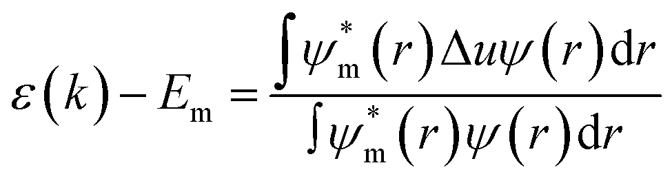
The simple tight-binding description of the energy levels of electrons ε(k) can be presented via eqn (1), wherein Em stands for the atomic energy level of orbital m, ψ and ψm are periodic and atomic wave functions, r is the location operator, and Δu is the perturbation potential coming from the periodic total potential. This formula can describe many physical aspects of chemical bonding inside the material based on tight-binding interpretations.
 | (1) |
 | ||
| Fig. 6 (a) Bismuth selenide bulk band structure. The colour code represents the projections of the pz Bi orbitals (red), pxpy Se orbitals (blue), and pz Se orbitals (green) in the wave function. The maximum and local maxima of the valence band are denoted by VBM and VBM′, respectively. (b) Band structure of the Bi2Se3 surface for different thickness values. Reprinted with permission from ref. 115. | ||
The most critical aspect of the theoretical calculations of bismuth selenide is the topologically protected metallic surface states forming a Dirac cone in the intra-band gap space in the band structure. This results in time-reversal symmetry preservation, nominating bismuth selenide as a topological insulator, with its accompanying specific potential applications (Fig. 7). One can make use of these surface states via engineering the surface-to-volume ratio of the corresponding nano-structures in experiments. In order to correctly calculate the surface state band structures in DFT programs, one approach is to use hybrid functionals together with spin–orbit coupling and smearing.5,116 Based on bulk theoretical calculations, the interlayer space between the surface layers and the impact of van der Waals forces on the corresponding band structure are also reported in ref. 88. It was found that the surface states are robust and protected under stress, and the pressure tends to increase the Fermi velocity of the surface electrons and the surface density of states at the bottom of the conduction band.89 Bouaziz et al. calculated the transition-metal doping of bismuth selenide and telluride [111] surfaces.117 The results were analysed with the Anderson impurity model, wherein the magnetic impurities open up a gap inside the Dirac cone. Fig. 7 shows the surface band structure of bismuth selenide calculated with the Quantum Espresso package. However, for very thin slabs, different thickness layers (quintuple layers) have different band structures at the Dirac cone, wherein a gap can open up for thin slabs; this has been explored theoretically and experimentally (Fig. 7 and 8).42,100,103 The theoretical description is reported in ref. 100. Wang et al. studied the magnetic quantum oscillations for surface states of 6 QTPL Bi2Se3 [111] surfaces via ab initio calculations, as reported in ref. 118. The Bi2Se3 electronic structure under stress has also been investigated,89 and it was found that the topologically protected surface states also remain robust under stress.
 | ||
| Fig. 7 Calculated surface band structure of bismuth selenide (9 QTPL) with different van der Waals gap expansions and the corresponding Rashba splitting and modifications on the Dirac cone states from ref. 88. Reprinted with permission from ref. 88. | ||
 | ||
| Fig. 8 Experimental ARPES spectra of a few quintuple layers of bismuth selenide from ref. 42. Reprinted with permission from ref. 42. | ||
The above-mentioned insights from theoretical calculations enable us to gain some perspectives for future research on bismuth selenide, both on the experimental and theoretical side, wherein one can predict and suggest, understand in-depth, design, and engineer new devices based on topological insulator bismuth selenide nanostructures, and shed light on the novel materials for future green energy applications. Here, we suggest using the concept of the Goldsmith rule for ion exchange within the lattice113 and a comprehensive check to make a library of various prototypes with different potential applications. Furthermore, due to the similarity of the layered structure of bismuth selenide with PbI2, the adoption of a two-step deposition method from perovskite solar cell materials119 for bismuth selenide can possibly allow the generation of new materials such as two-dimensional layered and hybrid 2D–3D structures, and the intercalation of different organic molecules in the interlayer spacings of the lattice. Moreover, the same chemical bonding concepts, i.e. the octahedral chemical bond length and angle impacts on the bandgap and material unit cell volume, and the corresponding tight binding description, can be explored to shed further light on this area and increase our basic understanding of this class of topological insulator materials.
5. Material synthesis
Different technologies have been used in synthetic methods for the formation of bismuth selenide to date. The reproducibility, stability, cost, time, ability to control growth, capability to integrate with device technologies, and accessibility are important factors when making a decision or deciding on a preference. In commercial applications, reaction time and the cost of the precursors and equipment play roles in determining the feasibility of the whole process. However, the growth temperature, control, and engineering of the growth, as well as how the material can be integrated/transferred into a target device structure, dictate the potential application of a method. In this section, we present examples of nanostructured growth and compare the methodologies; comparative summaries are presented in Tables 5 and 6.| Method | CVD | MBE | Chemical | Exfoliation |
|---|---|---|---|---|
| Cost | Medium | High | Low | Low |
| High-tech |  |
 |
X | X |
| Ease | Yes | No | Yes | No |
| Controllability | High | Excellent | Good | Low |
| Tedious |  |
 |
 |
 |
| Integrability | Decent | Decent | Difficult | More difficult |
| Method | Typical precursors | Temp./pressure | Morphology | Ref. |
|---|---|---|---|---|
| Melt grown crystal growth | Bi, Se powders | 850 °C | Crystal, single crystals | 110 and 134 |
| Bridgman method | Elemental Bi, Se | 750 °C | Crystals | 133 |
| Solvothermal hydrothermal | Bismuth: Bi, Bi(NO3)3·5H2O, BiCl3, Bi2O3 | About 200 °C | Nanowires, sheets, tubes, flakes, films, ribbons | 147–150 |
| Selenium: Se, SeO2, H2SeO3, Na2SeO3 | Autoclave (0.05 mTorr) | |||
| Several hours to 2 days | ||||
| Microwave-assisted synthesis | Bi, Se powders | 180 °C/1 minute/power of 1000 W | Nanowires, nanoflakes | 151 and 152 |
| BiO(NO3) | 2.45 GHz | |||
| Bi(NO3)3·5H2O | ||||
| Na2SeO3 | ||||
| Ethylene glycol | ||||
| SILAR | Bi(NO3)3·5H2O | Room temperature | Nanoparticulated film | 144 and 145 |
| Na2SeO3 | ||||
| On FTO | ||||
| MBE | Bi and Se sources | 300 °C | Thin film | 125 and 126 |
| PVD | Bi2Se3 powder | 3 mTorr | Thin film | 153 |
| Ar carrier gas | 700 °C | |||
| Si(100) substrate | ||||
| CVD | Bi2Se3 & Se powders | 550–700 °C | Nanowires, sheets, thin film | 154–156 |
| 8 × 10³ pascal | ||||
| PLD | Bi2Se3 target | Excimer laser | Thin film, hexagonal sheets | 142 and 143 |
| 5.5 J cm−2 | ||||
| 350 °C | ||||
| 4 × 10⁻⁶ Torr | ||||
| Exfoliation | Bi2Se3 material | On Si/SiO2 substrate | Layered film-nanoribbon | 35 and 124 |
| MOCVD | TMBi and DESe | 480 °C | Nanoflakes | 19 and 157 |
| Gold deposited Si | Hydrogen carrier | |||
| Patterning approaches | PDMS stamp | Ar carrier gas | Nano-sheet arrays | 146 |
| Bi2Se3 powder | 50 mTorr | |||
| Electrochemical deposition | Bi(NO3)3·5H2O, SeO2, HNO3 | Room temperature | Nanostructured film | 138 and 139 |
| On ITO | ||||
| Chemical bath deposition (CBD) | Bi(NO3)3·5H2O | 80 °C/200 min | 158 | |
| Na2SeO3 | On TiO2 | |||
| Sputtering | Bi2Se3 target | 3 mTorr Ar | Film | 137 and 159 |
| 30 W dc | ||||
| 10 W RF/425 °C | ||||
| Nano-sculpturing | Bi2Se3 flakes | Via TEM | Ring, wire, antidot, etc. | 141 |
5.1. Chemical vapor deposition (CVD)
Here, reactants in the gas phase are introduced and adsorbed on the substrate, where a chemical reaction takes place, and the nucleation and growth of the material continue. The CVD deposition of nanostructures takes place directly on the substrate, excluding the presence of solvent and additives, etc. Liu et al. have grown multilayered nanostructured bismuth selenide, where selenium and bismuth powders were evaporated in the CVD tube. The vapors were carried with argon gas to the silicon substrate, which was decorated with Au nanoparticles, at 550 °C.120 Brom et al., in another work,20 made Bi2Se3 hexagonal nanopillars using a sapphire [0001] substrate, at 220–540 °C, with trimethyl bismuth (TMB) and Se pillars as source, and hydrogen carrier gas. The temperature and growth procedure were optimized in order to have the best substrate coverage and fewer selenium vacancies (Fig. 9). High-quality platelets and nanoribbons of bismuth selenide of a few micrometres in size were grown by Alegria et al. via a metal organic chemical vapor deposition (MOCVD) method using diethyl selenium and trimethyl bismuth precursors, hydrogen carrier gas, 470 °C and 100 Torr chamber pressure, with a silicon substrate decorated with gold nanoparticles.19 The vapor–liquid–solid (VLS) mechanism can explain the growth mechanism of as-synthesized structures on gold-decorated silicon [100] substrates. | ||
| Fig. 9 SEM images of the bismuth selenide sheets grown via CVD at substrate temperatures of (a) 260 °C and (b) 280 °C. The insets show cross-section images of the sample. Reprinted with permission from ref. 20. | ||
Selenium vacancies are more likely to be formed during the growth due to a lower formation energy; therefore, a selenium-rich environment should be created inside the reaction tube, wherein the defect density can even be controlled via modifying the vapor pressure of the selenium.19,20 Thermodynamics, the relation between geometry, pressure, and temperature, concentration of the reactants, surface energies at boundaries, together with transport of the reactants via drift or diffusion, are key parameters. These factors rationalize the nucleation, growth, crystal orientation, vacancy concentration, and the physical properties of the as-grown products. Mica, graphene, and h-BN are other common substrates for the epitaxial growth of bismuth selenide via chemical or physical deposition techniques.
5.2. Chemical synthesis routes
Chemical reactions in solution are one of the most straightforward and widely implemented low-cost synthetic routes for the design and engineering of nanostructures of different types. Here, the growth mechanism depends on the temperature and pressure inside the vessel, the supersaturation fluid dynamics inside (e.g., stirring), time, the adsorption energies of additives and reactants on the nuclei crystallite, the zeta potential, and even the humidity and lighting in the environment. Therefore, the morphology, size, and quality of the as-grown nanostructures and the corresponding physics of the structures can be tuned. The selection of solvent and precursors, however, is more dependent on and restricted by the desired device with already deposited layers. Therefore, the post-deposition of the as-grown products on a substrate after the synthesis is the solution for device fabrication purposes. Herein, we present a few examples of this.The chemical synthesis of bismuth selenide via solution-processed methods (e.g. hydrothermal, solvothermal, etc.) results in very high-quality single-crystalline domain bismuth selenide hexagonal nanosheets. The typical precursors are selenium powder, bismuth nitrate, and conventional solvents such as water and ethanol. The surface adsorption and growth energy are very anisotropic for the rhombohedral lattice of bismuth selenide, with consecutive bismuth and selenide layers along the c-axis connected to each other through weak van der Waals forces. However, the chemical bonds with incoming atoms for in-plane atoms are of a covalent nature, and there is a directional preference for thermodynamically driven in-plane growth. This results in very high-quality hexagonal nanosheets with very fine facets and a thickness of a few layers (Fig. 10).
 | ||
| Fig. 10 (a) and (b) Optical image of the stacked Bi2Se3 nanoplates and AFM. (c) HRTEM and (d) electron diffraction pattern of the solvothermally synthesized bismuth selenide sheets by Liu et al. Reprint with permission from ref. 122. | ||
Razzaque et al.121 have grown bismuth selenide nano cubes (size less than 100 nm) via a colloidal route: injection of metal organic precursors at about 200 °C under a nitrogen atmosphere with vigorous stirring for water splitting purposes. The as-grown products were post-deposited on a glass substrate using aerosol spray deposition (with a rather poor adherence), and the growth parameters were optimized. The relevant stoichiometry of the resulting films was rather significantly tuned by temperature adjustment. A surface oxidation of the products, as studied by X-ray photoelectron spectroscopy (XPS), was due to the presence of a capping agent precursor in the solution.121
In the work of Pradhan et al., a different bismuth precursor, bismuth acetate, together with short-chain amines and acids and an organic solvent, octadecene, at a lower temperature of 100 °C, was used for the chemical synthesis of nanosheets.123 As doping in the solvothermal method is easily achieved via the addition of the dopant salt, the same methodology was implemented for the metal doping of bismuth selenide nanosheets, for example, in ref. 11 and 123.
5.3. Exfoliation
Liu et al.124 constructed a photodetector on a flexible substrate from bismuth selenide nanosheets with the exfoliation method (Fig. 11a). In summary, bulk bismuth selenide was ground in a mortar and then ultrasonicated with NMP solvent for 24 hours, washed, and dispersed in water. In this top-down synthesis approach, the mechanical forces exerted on the bulk bismuth selenide must be stronger than the vdW forces between the atomic layers, which results in cleavage and exfoliation of the material. One does not have full control of the crystallinity or shape of the structures. Bottom-up approaches, such as CVD and solvothermal methods, are more favourable for device applications; however, the top-down approach is attractive due to its low cost and simplicity. In another work, Hong et al. achieved more controlled exfoliation of QTLs using an atomic force microscopy tip (Fig. 11b) down to 1 QTL.35 Here, when the horizontal force induced via the AFM tip is large enough, the Bi–Se bonds can be broken; therefore, the upper part of the bismuth selenide will be scratched away. By controlling the lateral force and vertical position of the tip, it was possible to remove most of the upper QLs and leave intact ultrathin Bi2Se3 at the bottom.35 | ||
| Fig. 11 Exfoliated bismuth selenide. (a) SEM image of the sheets grown by Liu et al. Reprinted with permission from ref. 124. (b) AFM image of the nanoribbons. The exfoliation can be done until 1 QTL. Reprinted with permission from ref. 35. | ||
5.4. Molecular beam epitaxy (MBE)
In molecular beam epitaxy, one can control the film formation atom-by-atom. Here, at the expense of high vacuum and higher cost, one can obtain decent film quality and crystal growth. Precursor powders are heated up in a Knudsen cell with a typical pressure of 10−10 Torr and a substrate temperature of about 200 °C to give a uniform, thin film.125,126 In this way, with a suitable substrate, one can tune the thickness to a few QTLs. For example, in one of the very early experimental verifications of the Dirac cone in bismuth selenide, MBE was used to produce films with 1–6 individual QTLs.42 The deposition rate can be, for example, 0.67 Å per minute in this method.127 h-Boron nitrate,128 indium phosphate,129 silicon,130 SiC,42 aluminium oxide,125 and amorphous SiO2127 are among the substrates that have been used to date. In 2013, a 7QTL MBE-deposition of bismuth selenide on Bi2Ca2Cu2O8 superconductor resulted in the observation of a proximity effect and the discovery of superconducting states of a topological insulator surface. That was one step towards the observation of the formation of Majorana fermions in these materials.131 Springholz et al. performed Monte-Carlo simulations to simulate the MBE growth and compared the results with experimental data.1325.5. Other deposition approaches and crystal growth from solid-state reactions
For large-scale bulk single-crystals, different solid-state reactions from melts, such as the Bridgeman method,133 have been used, and we refer the reader to ref. 2, 13, 106, 110, 134 and 135 for further reading. Other deposition approaches, such as physical vapor deposition,136 sputtering,137 electrochemical deposition,138,139 bacteria-mediated growth,140 nano-sculpturing,141 pulsed laser deposition (PLD),142,143 and SILAR,144,145 have been implemented to deposit nanostructures of bismuth selenide. Lithographic approaches have also been implemented, coupled to patterning the nanostructures on the substrate using solvent stamping via van der Waals epitaxial growth, as reported by Zheng et al.146 In practical and commercial applications, however, a competition between the yield, cost, integrability, convenience, and time, etc., plays the main role in having a specific methodology for device fabrication. Table 5 compares different synthetic approaches in this context, and some typical examples, including the growth precursors, temperature, and pressure, are presented in Table 6.6. Characterization of bismuth selenide
Characterization is considered the basic tool to study, engineer, and predict the physical properties and potential device characteristics of bismuth selenide materials and devices. It is based on the related underlying fundamental physics and is of crucial importance for research development in this area. Different kinds of characterization, such as material physical characteristics measurement, advanced electronic structure and spin texture measurements, device stability against water and oxygen for long-term operations, and the collective ehavior of electronic charge and spin, are mainly classified within device and material characterization techniques. These have been determined both experimentally and theoretically. Among these techniques, there are various methods for the analysis of bismuth selenide, such as Raman spectroscopy,160,161 angle-resolved photoemission spectroscopy (ARPES),3,86 spin- and angle-resolved photoemission spectroscopy (SARPES),86,162 X-ray photoelectron spectroscopy (XPS),163,164 electron energy loss spectroscopy (EELS),163,165 ultraviolet photoelectron spectroscopy (UPS),166 scanning ehavior microscopy (STM),167,168 electrochemical characterization,121,169 Hall effect measurements,170 electron and neutron diffraction,171 Shubnikov-de Haas measurements,9,172 temperature-dependent conductivity and magnetoresistance (i.e. Hall measurements),57 thermal conductivity,173 magnetic susceptibility and torque magnetometry,168,174 X-ray absorption (XAS),175 atomic/Kelvin/piezoelectric force microscopy (AFM, KPFM, PFM),176 nuclear magnetic resonance (NMR),177 and terahertz and laser spectroscopy.17,178,179In order to highlight the topologically protected surface states and implement them for device application, one approach is to reduce the contribution from bulk states via bulk doping or having smaller nanosized structures with a higher surface-to-volume ratio. To characterize this, different techniques can be used. Zheng et al. introduced a new approach for enhancing bulk conductivity and improving the surface conductivity via tuning the formation of Bi2Se3 few-QTL films over Bi2Te3 few-QTL films with different thicknesses.180 In Hall conductivity measurements, however, the collective contributions from both bulk and surface states appear in the measured data. Instead, in terahertz spectroscopy measurements,179 one can measure, for example, the temperature dependence of mobility and the carrier density of surface states deconvoluted from bulk states.
Thermoelectric power generation is widely investigated and was the initial device target for bismuth selenide.181 Field-emission108 and field-effect transistors182 have also been studied extensively. Today, potential applications include photodetectors, batteries, medical imaging and cancer therapy, gas sensors, biosensors and more (see Section 7). These device architectures need their own characterization methodologies. Here, the semiconducting ehavior is in focus for device applications and the characterization of defect/doping density; Fermi level tuning is also an important issue. Superconducting states are also observed at low temperatures for Nb-, Sr-, and Cu-doped bismuth selenide materials.168,174,183
Bismuth selenide, as noted above, is an n-type semiconductor due to the thermodynamically favourable formation of selenium vacancies during growth. Shirodkar et al., in a computational/experimental study, showed that the selenium vacancy defect states can be healed via oxygen adsorption at the surface.184 Walsh et al.185 reported a very fine-tuned material with a nearly vacancy-free selenium synthesis of bismuth selenide with a Fermi level at almost the middle of the band gap. They also showed that, with careful annealing and monolayer de-capping, one can tune the Fermi level to near the upper half of the gap. In addition, chemical n-type/p-type switching of bismuth selenide nano-ribbons via reversible copper doping/intercalation was reported by Xiong et al.186
Energy levels of the photogenerated electron and holes, and their dynamics, i.e. time constants of thermalization and e–h recombination processes, are essential determining factors for device performance. Studied by Jnawali et al.17 via laser spectroscopy (mid-infrared femtosecond transient reflection) measurements, the thermalization kinetics of excited electron–hole pairs were estimated to be about a couple of picoseconds. The excited bulk carriers behave like a dense electron gas with recombination time constants of 150 ps and 50 ps at 10 K and 300 K, respectively. Electron–phonon interaction plays the key role in thermalization processes. Huang et al., in a combined study using time-resolved XRD and angle-resolved photoemission (ARPES) techniques, quantified the mode-specific electron–phonon couplings for the bismuth selenide and telluride surface states.187 Very recently, charge-transfer kinetics and electron–phonon dynamics of Bi2Se3 heterostructures with perovskite solar cell material CH3NH3PbBr3 have been investigated by Sharma et al., demonstrating their potential promise for solar cell applications.178
Local optical properties of CVD-grown bismuth selenide nano-sized beams (called nanobeams, with a mean size of about 700 × 300 nm) have been studied by Nandi et al.22 via nanoimaging phase mapping characterization. The as-grown films show a very high refractive index of 6.4 for mid-infrared light, and the phase mapping reveals local domains with different shifts and different scattering yields for unpolarized and different polarized light. This thus provides information about the local optical properties of bismuth selenide nanostructures.22 Das et al. studied the visible-light optical properties of PVD-grown films annealed at different temperatures.24 Ellipsometry measurements of bismuth selenide optical properties for different nanostructures of bismuth selenide were reported by Yang et al.188
The bismuth selenide structures tend to be protective and robust against water and oxygen (air attack), which is essential for device operation. The water and oxygen stability of bismuth selenide was studied,164 and it was shown that there is negligible reactivity of bismuth selenide with water and oxygen, and the surface oxidation of bismuth selenide in dry air takes place on the time-scale of years. This, together with the higher stability and lower degradation of the structure with topologically protected surface states, makes them good potential candidates for several applications. For example, field-emitters based on bismuth selenide are reported to show a turn-on voltage of 2.5 V µm−1 and a current density of about 180 µA cm−2.108 Theoretical calculations show that, even in the case of oxidation, the topologically protected surface states remain robust and the electronic structure of the surface states remains unchanged.189 A similar metal chalcogenide compound based on tin, Sn(S0.92Se0.08)2, implemented in tin-based perovskite solar cells as a charge-selective layer to suppress the well-known oxidation of Sn cations inside the film by circumventing the oxygen desorption, enhances the stability of the solar cell. Suitable energy levels and excellent stability against water and oxygen resulted in a high-performing, highly stable perovskite solar cell, with a power conversion efficiency (PCE) of 11.78%.190
Surface wettability is an important factor for both device stability issues and liquid-phase deposition of extra layers in device fabrication. The surface wettability of PVD-grown bismuth selenide was studied by Das et al.24 They annealed the films under different temperatures and found that the crystallite size increases from 14 nm, for films without annealing, to 24 nm, for films annealed from 100 to 250 °C. The contact angle with water showed an increase from 99 to 120°, respectively. Goncalves et al., however, showed the presence of other BixSey phases inside the bismuth selenide after annealing at temperatures higher than 300 K.191
The characteristics of other bismuth chalcogenides, such as bismuth telluride and sulphide, also led to a better understanding and rapid development of devices based on Bi2Se3 materials. Fig. 12 presents a few results of experimental characterizations of bismuth selenide materials and devices mentioned above.
 | ||
| Fig. 12 Examples for experimental characterizations of the bismuth selenide materials and devices. (a) SARPES spectrum showing the electronic spin texture. Reprinted with permission from ref. 162. (b) Typical torque curves measured from torque magnetometry at 0.3 K. Reprinted with permission from ref. 174. (c) XPS spectra and the corresponding evolution of bismuth and selenium core electrons before and after exposure to humidity. Reprinted with permission from ref. 164. (d) Contact angle images of the samples annealed at different temperatures. Reprinted with permission from ref. 24. (e) A typical transient reflectance spectrum measured at 300 K and 10 K with a pump wavelength of 1.5 eV. Reprinted with permission from ref. 17. (f) Transient absorption spectra for the MAPbBr3 perovskite heterostructure with bismuth selenide, showing the signature of the photoinduced absorption and ground-state bleach. Reprinted with permission from ref. 178. | ||
Point defects are widely implemented to tune material optoelectrical properties. Our understanding and level of control of mesoscale defects and domains in bismuth selenide is rather limited so far, and new probes to characterize the relevant carrier dynamics necessitate novel probing tools to specifically study the topologically protected surface states and corresponding optical properties.192 On the other hand, in order to specifically probe transitions between the surface-protected states, a joint theoretical/experimental approach with new characterization methods seems to be crucial to achieve a full understanding and the complete picture of Bi2Se3 photophysics. Still, the picture is not complete, and many recent publications trends are moving in this direction.
7. Green energy devices based on bismuth selenide
7.1. IR-Photodetectors
Infrared photodetectors have a wide range of novel applications in the military and space industries, astronomy, and remote imaging. Here, different materials have their own benefits and drawbacks, and the commercial ones produced in the military and, for example, NASA, for the detection of black holes in astronomical applications, still need further development. Bismuth selenide is one of the materials with a band gap lying in the far-infrared/terahertz region, making it potentially ideal for such applications. However, IR detectors based on photovoltaic, photoconductivity, and photothermoelectric effects have different underlying mechanisms. They stem, respectively, from self-driven selective accumulation of opposite charges under illumination, incoming photon-triggered enhanced conductivity, and thermal-gradient-based electrical currents based on heating effects. One needs to use the proper characterization technique and modify the conductivity, mobility, absorption coefficient, exciton lifetime, electron transport time, etc., in order to control and improve device performance. Here, the most important parameters for characterization and practical potential investments are noise ratio (ratio between light and dark currents), detectivity, responsivity (ratio of incident photon flux Pin and the output current Ip), and response time (time span for photocurrent rise after light-on), which are briefly described in ref. 193. We refer the reader to ref. 194 for more information about different working conditions and mechanism types in infrared photodetectors and commercial examples.Liu et al. reported the implementation of bismuth selenide nanosheets in a device based on a paper substrate that showed excellent responsivity at 1064 nm IR light, with acceptable stability under different bending conditions.124 Here, the IR light-driven photoconductivity of bismuth selenide detects the incidence of infrared light (Fig. 13).
 | ||
| Fig. 13 (a) Schematic of a bismuth selenide infrared photodetector device based on a flexible paper substrate. (b) Illustration of the corresponding photocurrent measurement. (c) Photocurrent rise and decay time (response time) under consecutive turning on/off of the incident light under different bending conditions. Reprinted with permission from ref. 124. | ||
Zhang et al. fabricated a high-performance photodetector device based on n-type silicon and a bismuth selenide heterojunction structure (Fig. 14).195 In a separate study, Wang et al. used a heterojunction IR detector based on bismuth selenide/WO3, wherein the interface band bending reduced the dark current noise and enhanced the charge separation efficiency inside the device. This results in a 2D Bi2Se3/Wse2 responsivity of 3 A W−1 and a detectivity of 2.2 × 10¹⁰ Jones for 1456 nm infrared.196
 | ||
| Fig. 14 (a) Schematic of the heterojunction device based on bismuth selenide and the (b)–(f) device characteristics. (b) Dark current, (c) photovoltaic effect under sunlight, (d) photocurrent under 808 nm NIR, I photocurrent response spectrum and (f) absorption spectra of the device with different thicknesses. Reprinted with permission from ref. 195. | ||
Efforts have been made to construct bismuth selenide-based photodetectors both theoretically and experimentally; however, the field is still rather young and remains at the research and development stage. More studies are needed to fully understand the underlying physics and overcome the current practical limits, such as slow response times (on the time-scale of seconds). Flexible photodetectors and wearable and portable devices, polarization-sensitive detectors, heterojunction detectors, and doping effects are among the studies that have been reported recently.124,146,195–197 Moreover, the surface-protected topologically preserves the surface states of bismuth selenide and the formation of spin-coupled Dirac branches with spin-momentum lock (see Section 3.3), making them specific for polarization detection capabilities, such as that reported in ref. 27 and shown in Fig. 3. Furthermore, similar efforts have focused on bismuth telluride and also mixed phases such as Bi2SeTe, Bi2SexTe2−x, and Bi2SexTeyS2−x−y in order to further explore and expand the material properties and corresponding device performances, which are beyond the scope of the current review.
Sharma et al. demonstrated that focused ion beam (FIB) fabricated Bi2Se3 nanowires can act as ultrasensitive photodetectors for visible and near-infrared light, achieving a photoresponsivity of approximately 300 A W−1.198 Zheng and colleagues developed a method combining micro intaglio printing with van der Waals epitaxy to create large-area Bi2Se3 arrays, and reported an external photoresponsivity of about 1650 A W−1.146 This technique enabled the creation of large-area arrays of Bi2Se3 topological insulators, achieving a record Hall mobility of approximately 1750 cm2 V−1 s−1 at room temperature. Additionally, their patterned crystal arrays were successfully integrated into flexible photodetectors.
Liu's study focused on understanding how precursor temperature affects the growth of Bi2Se3 nanobelts for NIR photodetectors, yielding ultra-fast photoresponses and high detectivity.199 Hong et al. fabricated Bi2Se3 films on micro pyramidal silicon, enhancing light trapping and achieving excellent performance across a range of wide wavelengths.136 The etching process was crucial for improving the photoresponse, and the devices demonstrated optimal performance after 30 minutes of wet etching. Overall, the micro pyramidal structure significantly boosts the photodetection capabilities of the Bi2Se3/Si heterojunction, indicating strong potential for infrared detection applications. Yang et al. introduced a Bi2Se3/MoO3 heterojunction that exhibited exceptional responsivity and detectivity over a broad spectrum.200 The response time was 63 microseconds, which is significantly faster than ordinary bismuth selenide-based photodetectors.
Das et al. created a heterojunction of Bi2Se3 nanoflakes and silicon nanowires, achieving a maximum photoresponsivity of 934.1 A W−1.201 They characterized the device by analysis of the temperature-dependent barrier height and ideality factor of the junction. Li et al. fabricated a copper-doped Bi2Se3/p-Si heterostructure, significantly improving the photocurrent after doping; i.e. a 42-fold increase compared to intrinsic bismuth selenide.202 Lu's work on a cascade heterostructure of bismuth chalcogenides demonstrated outstanding photodetector performance.203 The convenient charge transport/transfer within this cascade heterostructure, together with high incident-photon-to-current-efficiency (IPCE), makes it possible to also implement them as a photoelectrochemical splitting device for water splitting. Tang et al. introduced sub-millimeter terahertz detectors using a metal–topological insulator–metal heterostructure, achieving high responsivity and fast response times.204
Fig. 15, 16 and Table 7 summarize recent efforts and compare the corresponding performances, presenting a schematic diagram of various photodetector devices based on Bi2Se3, the performance of the Bi2Se3 photodetector in terms of photocurrent switching, and a summary of the performance of different Bi2Se3 photodetectors. Overall, these studies underscore the versatility and performance of Bi2Se3, positioning it as a key material for advancing photodetector devices.
 | ||
| Fig. 15 Schematics of (a) the device based on a heterojunction between Bi2Se3 and silicon, reprinted with permission from ref. 196, (b) the single Bi2Se3 nanobelt NIR devices, reprinted with permission from ref. 199, and (c) a Bi2Se3/n-type silicon-based device, reprinted with permission from ref. 136. (d) Bi2Se3/Si-Nanowire heterojunctions, reprinted with permission from ref. 201, and (e) the vertical nanoplates of copper-doped Bi2Se3/Si heterostructure photodetector device, reprinted with permission from ref. 202. | ||
 | ||
| Fig. 16 Photocurrent switching performance of (a) the Bi2Se3 nanobelt photodetector, reprinted with permission from ref. 199, (b) Bi2Se3 structures grown on the pure Si substrate and Si nanowires, reprinted with permission from ref. 201, (c) the Cu-doped n-Bi2Se3/p-Si photodetector under 900 nm and 146 W m−2 light illumination with 3.87 atom% Cu concentration under different light intensities, reprinted with permission from ref. 202, and (d) the Bi2Se3 flake photodetector at a bias voltage of 1 V and an illumination power of 142.93 mW cm−2, reprinted with permission from ref. 205. | ||
| Materials | Detector | Growth method | Detectivity (Jones) | Responsivity (A W−1) | Risetime (s) | Ref. |
|---|---|---|---|---|---|---|
| Bi2Se3 nanosheets | IR photodetector | Liquid exfoliation | — | 26.69 × 10⁻⁶ | — | 124 |
| Bi2S3 nanosheets | Photoelectrochemical (PEC)-type photodetector | Liquid phase exfoliation (LPE) | 9.93 × 10⁷ | 210 × 10−6 | 0.1 | 206 |
| Bi2Se3 (thick flakes) | THz detector | — | 2.17 × 10¹¹ | 75 | — | 204 |
| Cu-doped n-Bi2Se3/p-Si | Heterostructure photodetector | CVD | 1.85 × 10¹¹ | 168.9 × 10⁻³ | — | 202 |
| Bi2Se3 (thin film)/MoO3 | Heterojunction photodetector | MBE | 5.79 × 10¹¹ | 2609 | 62 × 10−6 | 200 |
| Bi2Se3/Si (nanowire) | NIR photodetector | Wet chemical route | 2.30 × 10¹³ | 934.1 | 0.041 | 201 |
| Bi2Se3/Si | NIR photodetector | Wet chemical route | 7.2 × 10¹² | 287.7 | 0.11 | 201 |
| Bi2Se3 (nanowire) | NIR-detector | Focused ion beam (FIB) | 7.5 × 10⁹ | 300 | 0.55 | 198 |
| Bi2Se3 nanosheet (exfoliated) | Photoelectrochemical (PEC)-type photodetector | Hydrothermal | — | 20.48 × 10⁻³ | 0.7 | 207 |
| Bi2Se3 nanobelts | NIR photodetector | van der Waals epitaxy | 4.63 × 10⁸ | 10.1 × 10⁻³ | 0.037 | 199 |
| Bi2Te3/Bi2Se3/Bi2S3 | Photoelectrochemical (PEC)-type photodetector | Sequential vapor phase deposition | 8.96 × 10⁹ | 103 × 10−3 | 8 × 10⁻³ | 203 |
| Bi2Se3 (nanowire)/Si | Heterostructure photodetector | Thermal evaporation | 2.38 × 10¹² | 924.2 | 0.045 | 208 |
| Bi2Se3/micropyramidal Si | Heterojunction photodetector | PVD | 1.24 × 10¹¹ | 7.16 × 10⁻³ | 0.52 × 10⁻³ | 136 |
| Bi2Se3 flake | IR photodetector | van der Waals epitaxy | 3.3 × 10¹⁰ | 2.74 | 0.54 | 205 |
| Bi2Se3 flake (T = 80 K) | IR photodetector | van der Waals epitaxy | 8.0 × 10¹⁰ | 23.89 | 0.54 | 205 |
| Bi2Se3/Si Heterostructure | Heterostructure photodetector | Epitaxial growth | 4.39 × 10¹² | 24.28 | 2.5 × 10⁻⁶ | 195 |
| 2D Bi2Se3/WSe2 | Visible and NIR detector | van der Waals heterostructures | 2.2 × 10¹⁰ | 3 | 4 × 10⁻³ | 196 |
To engineer and design new materials with enhanced properties for photodetectors, one needs to systematically probe the material library space and use fundamental insights from chemical bonding prospects and fine-tune the desired aspects. Alloying and mixing compounds with other bismuth chalcogenides offers great possibilities to shed further light on the development of bismuth selenide-based photodetectors. Photodetectors based on topological insulator materials are reported in ref. 209, and more informative reports about bismuth chalcogenide-based photodetectors are listed in ref. 210–212. Further insights can be elucidated from X-ray photodetector/scintillator devices based on various bismuth compounds, wherein the high atomic number of bismuth is very beneficial for high X-ray attenuation.213
7.2. Spintronics and quantum computing
Bismuth selenide is a prominent topological insulator that has gained considerable attention in the field of spintronics due to its unique electronic properties, spin-momentum locking, and the presence of protected surface states. Integrating Bi2Se3 with ferromagnetic materials has opened new avenues for exploiting magnetoelectric effects.1,214,215 These studies have explored how electric fields can influence magnetization and spin transport, potentially leading to innovative spintronic devices that leverage the interplay between charge and spin currents.216 The bismuth selenide Dirac cone in the band gap allows the surface state electrons to have a very high velocity, mobility, and long spin diffusion length and mean free path, which is very attractive for spintronic devices. Furthermore, for the surface state electrons, the spin is locked to the momentum, which means that different spin currents can propagate in different directions in the presence of magnetic interactions with ferromagnetic layers. By leveraging the robust spin-polarized surface states of Bi2Se3 and investigating the effects of defects and heterostructure configurations, the studies collectively advance the energy-efficient technologies capable of manipulating spins via electrical means. This comprehensive approach positions Bi2Se3 as a cornerstone material for future developments in memory and logic devices within the spintronics landscape.217 Here, we summarize a few examples from recent efforts to manipulate and engineer spin or spin-locked currents for potential spintronic and quantum computing applications.In an investigation by Tang et al. into the quantum transport properties of heavily doped Bi2Se3 nanoribbons, it was revealed that manipulating defects and doping levels can further enhance the spin transport characteristics, which is crucial for device performance.57 Jozwiak et al. contributed to this understanding by examining the control of spin-polarized surface states, demonstrating that external magnetic and electric fields can effectively manage the spin dynamics—an essential factor for functional spintronic applications.218 Mellnik et al. focused on the generation of spin–orbit torque in Bi2Se3, providing evidence that this material can efficiently convert charge currents into spin currents.219
In addition, Bi2Se3 also shows promise in quantum computing (see Section 3.4). However, defect-induced bulk carriers can obscure the valuable surface states essential for these applications. Abhiram et al. explored isoelectronic doping through ion irradiation using 600 keV antimony (Sb+) ions on Bi2Se3 thin films. Their findings, based on Rutherford backscattering spectroscopy, revealed that heavy irradiation altered the magnetoresistance from a parabolic to a linear response, which was attributed to mobility fluctuations. This study highlights ion irradiation as an effective method for tuning quantum coherence phenomena in Bi2Se3, potentially enhancing its properties for both spintronic and quantum applications (Fig. 17).220 By carefully controlling the doping, mobility, structural integrity, and quantum coherence, it is possible to enhance the efficiency and functionality of spintronic configurations, paving the way for advanced applications in next-generation electronics.220
 | ||
| Fig. 17 Schematic of deposition, Sb-irradiation, and post-irradiation annealing of a Bi2Se3 thin film. Reprinted with permission from ref. 220. | ||
Li et al. investigated spin currents in Bi2Se3 by utilizing tunnelling ferromagnetic (FM) contacts while applying a charge current to the surface.221 Their results indicated that the momentum direction of the carriers k locks the spin direction along the y-axis, which is detectable via the FM contacts (Fe). The magnetic field-dependent voltage measured between the FM contacts and an Au contact showed sharp increases or decreases as the magnetization of the Fe electrode switched, depending on the alignment of the magnetization direction with the carrier spins221–223 (Fig. 18).
 | ||
| Fig. 18 Spin transport in the surface metallic states of topological insulators (TIs). (a) Schematic of the spin momentum locking in the Dirac band of the TI surface states. Reprinted with permission from ref. 224. (b) Conceptual illustration of the TI spin transport device structure, featuring a ferromagnetic (FM) electrode to measure the spin polarization of the conducting carriers. (c) and (d) Spin-dependent voltage as a function of the magnetic field for positive and negative 2 mA currents, respectively. Reprinted with permission from ref. 221. | ||
A promising application of the spin Hall effect is the manipulation of the magnetization of an adjacent ferromagnetic layer through spin–orbit torque (SOT), i.e. switching the magnetic moment for adjacent ferromagnetic layers. Spin–orbit torque relies on the generation of spin current from charge current in a nonmagnetic material, which is a critical topic for spintronic devices and promises to provide an energy-efficient scheme for manipulating magnetization in magnetic devices.225 The spin-momentum locking present in the surface metallic states of topological insulators (TIs) provides an effective means of generating spin currents and three-dimensional topological insulators; especially, bismuth selenide shows orders of magnitude improvement in SOT efficiency at low temperature.224 A notable breakthrough in this area was the observation of substantial spin–orbit torque at the Bi2Se3-permalloy (Py) interface, where Bi2Se3 exhibits metallic behaviour.219,222 Researchers have employed spin-torque ferromagnetic resonance measurements to probe two distinct torques—spin–orbit torque and Oersted field torque—around the resonance condition of the Py thin films.222,223 Mellnik et al. achieved a SOT efficiency of 2.5 and spin conductivity of 110–200 × 103 ħ 2 eΩ−1 m−1 for the Bi2Se3/Py junction.219 Han et al. implemented a Bi2Se3/CoTb layer with perpendicular magnetic anisotropy at room temperature and showed switching via current-induced magnetization, as presented in Fig. 19.226 A similar work on BixSe1−x/Ta is presented in Fig. 19b from ref. 227.
 | ||
| Fig. 19 Current-induced magnetization switching in bismuth selenide-based architectures (a) Bi2Se3/CoTb and (b) BixSe1−x/Ta. Reprinted with permission from ref. 226 and 227. | ||
Magnetic doping is crucial for breaking time-reversal symmetry in the surface states of TIs, leading to novel physical phenomena and technological applications. Liu and colleagues focused on chromium-doped Bi2Se3 in its ultrathin form, which is anticipated to exhibit the quantum anomalous Hall effect (QAHE)228 (Fig. 20). They successfully produced high-quality Bi2xCrxSe3 epitaxial thin films using molecular beam epitaxy (MBE). Their findings suggest that the coexistence of ferromagnetic and antiferromagnetic chromium defects accounts for the lower magnetic moments observed in conventional magnetometry, which are significantly below the 3μB per chromium atom predicted by Hund's rule.228 The ferromagnetic quantum anomalous Hall effect was separately observed by Moon et al. in a Cr-doped 10-QL Bi2 Se3 layer on Al2O3 substrate. They also studied the shape of the hysteresis/magnetoresistance relation via a tight-binding model and demonstrated that the Berry phase calculations, including the Cr-induced Zeeman effects, can reproduce the QAHE results.229
 | ||
| Fig. 20 Schematic of the experimental setup for the quantum anomalous Hall (QAH) effect measurement. Reprinted with permission from ref. 228. | ||
7.3. Solar cell devices
Perovskite absorbers have no response in the IR region, and the incorporation of bismuth selenide can enhance the performance of perovskite solar cell devices in this region. High charge mobility and tuneable p-type/n-type behaviour are also considered beneficial for bismuth selenide materials for charge-selective layer implementation. In the solar cell industry and based on the device structure (i.e. a three-terminal tandem, a flexible transparent, or a stand-alone commercial one), we need to use and design new materials that have the best efficiency, cost, toxicity level, and weight, etc. Here, bismuth selenide and its counterparts bismuth telluride/sulphide have been tested in different solar cell devices, both as (co-)absorber and charge transfer layers. They are implemented in order to increase the charge mobility and reduce trapping/recombination drawback effects or optimise the light-absorption capability in the IR region. Supekar et al. collected recent efforts for the implementation of bismuth sulphide and antimony sulphide counterparts in solar cell devices in ref. 230.Bismuth selenide (band gap 0.3 eV) does not have the best band gap for solar light absorption in solar cells; therefore, it is not fundamentally interesting as a key component main layer in solar cell materials. However, it has been implemented as an additive in dye-sensitized solar cell anode or cathode electrodes231,232 and in perovskite solar cell233 charge transport layers. Other bismuth chalcogenides, such as bismuth telluride and sulphide, have also been implemented as electron and hole transport layers in high-stability, high-efficiency normal and inverted perovskite solar cells, improving the ambient stability of the device as reported in ref. 234 and 235; it has even been used as a hole transporter in organic solar cells.236 As an additive, it can enhance the charge transport, carrier lifetime, collection efficiency, infrared absorption, and the overall power conversion efficiencies, and it can improve the electrocatalytic activity of the counter electrode. It has also been explored theoretically.233 The similar compound, bismuth sulphide, however, fulfils the bandgap criteria for being a good solar absorber and, to date, has been implemented both as a solar absorber layer and a transport layer for perovskite solar cell devices.235,237,238 Very recently, a similar tin chalcogenide has been used as an electron transport layer to enhance the stability of tin-based perovskite solar cells.190 The special surface-related properties of bismuth selenide have been considered for novel charge transport layers in perovskite solar cells. For example, the charge transfer kinetics at the interface of lead perovskite absorber material with Bi2Se3 have been studied using laser spectroscopy178. Fig. 21 show few examples of the above mentioned works.
 | ||
| Fig. 21 (a) Schematic of the organic cell device with the Bi2S3 counter electrode and (b) and (c) power conversion efficiency of the device after aging and comparison of incident photon to current efficiency (IPCE) with a typical MO counter electrode. Reprinted with permission from ref. 231 and 236. (d) and (e) SEM and TEM images of bismuth selenide nanostructures used as an additive in the dye-sensitized solar cells and (f) the PCE improvement with bismuth sulfide additive. Reprinted with permission from ref. 231 and 236. | ||
7.4. Charge storage devices
Bismuth selenide materials have been implemented as electrode materials for ion batteries and supercapacitors. There is more room for bismuth selenide nanostructures for charge storage devices research, and even its composites with carbon have shown very good results. The layered, stacked structure of the bismuth selenide and the high surface-to-volume ratio of its nanostructures provide a high ion diffusivity and charge transfer in the electrode. Moreover, they usually show high stability in batteries. Zhao et al., in a recent work,165 proposed a few-layer bismuth selenide as a cathode material in quasi-solid Zn ion batteries with anti-freeze hydrogel electrolyte, and characterized the battery at low temperature (−20 °C). The delivered capacity was 1.5 times higher than at room temperature with the same specific current. A high stability of about 95% retention after 2000 cycles at 1 A g−1 was obtained. They showed that zinc ion uptake at the few-layer bismuth selenide is higher at lower temperatures; i.e. about 6 Zn2+ ions are uptaken at −20 °C and four ions are uptaken at 25 °C. This unusual behaviour only happens for the few-layer bismuth selenide and not for its bulk counterpart, and can be related to the topologically protected surface states and weaker phonon vibrations at low temperatures. Therefore, this bismuth selenide-based electrode can be a choice for charge storage and powering of devices operating at low temperatures for extended periods. Fig. 22 shows the electrochemical characterization of the battery, cycle retention, and corresponding bismuth selenide volume changes after intercalation of zinc ions. | ||
| Fig. 22 Zn ion battery based on a bismuth selenide cathode (a)–(c) cyclic voltammetry, specific capacity at different temperatures, and cycle retention after 2000 cycles at 0 °C. (d) The corresponding temperature-dependent unit cell volume changes after intercalation of zinc ions at the cathode. Reprinted with permission from ref. 163 and 165. | ||
Xingxing Zhao et al.239 used bismuth selenide with a carbon coating, Bi2Se3@C, in the cathode of potassium ion batteries, which involved an alloying redox reaction. It shows a very high reversible capacity of 526 mAh g−1 at 50 mA g−1 specific current and very high stability after 1000 cycles of charge–discharge. A micro supercapacitor was made by Hao et al.46 with a high specific capacitance of 272.9 F g−1. The high electrochemically active surface of bismuth selenide, which arises from its layered quintuple-layer structure, is considered responsible for the favorable reversible redox performance. A large capacitance, high power density, and 95.5% retention after 1000 cycles were obtained for the flexible all-solid-state capacitor made of Bi2Se3.
Meja et al. characterized bismuth-selenide-based anode electrodes for aqueous sodium ion batteries via electrochemical techniques. They found a two-order-of-magnitude improvement in the diffusion coefficients in comparison to other similar anodes for sodium ion batteries. However, the stability is still an issue, which needs to be considered for practical applications.169 A schematic of the cell and the results are shown in Fig. 23.
 | ||
| Fig. 23 (a) Schematic of the electrochemical cell. (b) and (c) Cyclic voltammetry and charge/discharge curves for the bismuth selenide electrode in the lithium ion battery from ref. 169. The differences in the CV graphs correspond to different reactions or charging/discharging phenomena at the electrode interface. Reprinted with permission from ref. 169 (d) and (e) cyclic voltammetric graphs of bismuth selenide @C electrode for the lithium ion battery at different scan rates and the corresponding diffusive and capacitive contributions in total capacitance measured at different scan rates. Reprinted with permission from ref. 240. | ||
Kumari et al. employed bulk and nanostructured bismuth selenide in all-solid-state lithium-ion batteries as the anode and achieved acceptable performance. The thermochemical reaction between the solid electrolyte and selenium produced in the de-lithiation process results in loss of cycle stability. However, they showed that the nanostructured film based on nanoparticles and nanosheets enhances the stability compared to that of the bulk counterpart, with excellent discharge capacity.241 Basically, two different contributions from capacitive and diffusive charging can happen at the electrode, with different reaction features in the cyclic voltammogram (Fig. 23c and d).169 Several studies have been pursued to investigate, implement, and engineer ion batteries based on bismuth selenide alone or composites thereof, in an effort to improve the stability and performance, or to study the physical chemistry of the reactions at the interfaces.240,242–244 Theoretically, bismuth selenide has a high specific capacity for alkali-ion storage due to its layered structure and large interlayer spacing.
After the achievement of successful results for bismuth selenide-based potential lithium-ion batteries, more studies on zinc, magnesium, potassium, and sodium ion batteries have also been conducted. These were accomplished with a variety of implemented materials such as bulk, nanostructured, doped, nanocomposite, and metal–organic frameworks, all based on bismuth selenide. Here, the drawback can be the stability issue, i.e. poly-selenide shuttle formation, pulverization,245 and excess volume expansion of the layered bismuth selenide electrode after the ion intercalation, which affects the stability. Bismuth selenide nanostructures instead provide more surface sites and more space for the bulk expansion. Zhu et al. modified bismuth selenide electrodes with nitrogen-doped Bi2Se3−xTex nano materials, which show a stable discharge capacity of 464 mAh g−1 after 60 cycles at a charge density of 0.1 A g−1. Its unique structure mitigates the volume expansion issue and increases the stability of the cell.246 In a recent work, Zou et al. implemented the Sb-doped bismuth selenide, decorated and encapsulated with nitrogen-doped carbon, as an anode material for lithium-ion batteries.245 They showed that the electrochemical performance was improved and the shuttling of poly-selenide was suppressed after doping/encapsulating the bismuth selenide.
Ni et al., in a separate report, discussed and compared the challenges and recent efforts for the implementation of bismuth chalcogenide electrodes in electrochemical devices, such as ion batteries and supercapacitors. The key technical issues for material development for novel, more stable, and high-performance devices were highlighted.247 One key feature is the layered structure of bismuth telluride and selenide, with van der Waals interlayer interactions, leading to possibly less stable electrodes in cell cycling; however, this makes more room for a higher ion uptake. The bismuth sulphide and oxide possess, however, different crystal structures and show a higher stability. Engineering of band edges based on the chemical bonding concepts is a facile route to achieving different electrochemically active windows in electrochemical applications.
7.5. Biosensors and gas sensors
Due to its high electrocatalytic activity, high surface-to-volume ratio of its nanostructures, high charge-carrier density, and the presence of plasma resonance, bismuth selenide has been widely used as a material for urea, glucose, ammonia, and atenolol biosensors. Together with its imaging, cancer therapy, antimicrobial, and even drug-delivery properties, bismuth selenide shows great potential for application as a future medical agent. Fudan Zhu et al. considered a multiwall carbon-modified bismuth selenide as an electrochemical biosensor, with promising performance for nitrile detection (up to 0.01 µM).248 Higher electron-transfer rate and active surface area were mentioned as reasons for the high detectivity of this biosensor for the detection of nitrile in food and the environment. Savariraj et al. constructed a biosensor from a few-layer bismuth selenide material made via microwave-assisted synthesis.249 The resonant plasma frequency and high electrocatalytic activity of Bi2Se3 were suggested to promote the high level of glucose detection (up to 6 µM). This sensor reaches the steady state within 3 seconds after glucose introduction and maintains the steady state for up to 19 days.Lingping Xiao et al. demonstrated the use of Au nanoparticles decorated with bismuth selenide as an electrochemical colorimetric biosensor.250 Here, the solution colour change showed the ‘switch-on’ and ‘switch-off’ of the biosensor. The cancer biomarker is the CEA, and the presence of antibody-CEA or antigen-CEA can turn on or off the catalytic activity of the bismuth selenide electrode. Fig. 24 shows a schematic of the sensing mechanism, together with TEM images of the gold-decorated bismuth selenide sheets and the catalytic activity of the structure for the reduction of 4-nitrophenol in the presence of different concentrations of antCEA.
 | ||
| Fig. 24 (a) and (b) TEM images of the gold-decorated bismuth selenide sheets implemented in the calorimetric biosensor. (c) and (d) Catalytic activity of the bismuth selenide structure and the corresponding absorbance change for the reduction of 4-nitrophenol in the presence of different concentrations of anti-CEA. (e) Schematic of the sensing mechanism in the presence of antibody-CEA and antigen-CEA. Reprinted with permission from ref. 250. | ||
This shows a very high selectivity and sensitivity even for very low CEA concentrations of 160 pg mL−1, which was confirmed via real clinic sampling and analysis. The corresponding catalytic activity of this electrode was compared to other similar works in ref. 250. It shows that using a much lower amount of material, better or much better catalytic activity was achieved for the reduction of 4-nitrophenol.
The gas-sensing properties of Bi2Se3 were investigated in ref. 251 and 252. van der Waals layered structures usually do not have dangling bonds at the surface, and gas sensing capabilities are limited. However, through, for example, creating two-dimensional nanoscale and edge features251 or inducing epitaxial growth, one can reach the desired electronic properties. For NO2 gas sensing, a high response of 93% at 50 ppm has been reached via a bismuth selenide nanosheet layer in a chemi-resistive gas sensor with anti-humidity capability (Fig. 25).252
 | ||
| Fig. 25 Resistance variation of a chemi-resistive gas-sensor based on bismuth selenide under exposure to different gases. Reprinted with permission from ref. 252. | ||
In a separate study, Yi et al. measured the NO2 sensing properties and its underlying mechanism for bismuth selenide/tin selenide hexagonal sheets heterostructure. It shows a rather fast detection of 15 seconds at room temperature and a detection limit of 25 pbm.253 The gas sensor also showed a good selectivity for NO2 between the tested gases such as H2S, NH3, CH4, CO and SO2.
7.6. Antimicrobial effects and medical applications
The bismuth selenide surfaces can be effective antimicrobial surfaces, as reported previously, for example, by Jiang et al.,254 who showed that 80 nm bismuth selenide sheets, together with hydrogen peroxide, presented as a new type of insecticide and biocompatible surface. In vitro and in vivo studies show that the growth of Escherichia coli and Staphylococcus bacteria is significantly suppressed (Fig. 26). | ||
| Fig. 26 TEM image of the implemented bismuth selenide nanosheets and optical images of bacteria growth on the control and antimicrobial surfaces. Reprinted with permission from ref. 254. | ||
Recently, nanomedicine and bioengineering have made it possible to perform diagnosis and therapy simultaneously. This safely enhances cancer immunotherapy and tumour imaging.255 The main benefits and characteristics are non-toxicity and biocompatibility, the ability to convert biofriendly infrared light into heat and subsequent active electron hole charges for chemical and biochemical reactions, the high X-ray attenuation coefficient of bismuth, the ability of selenide to reduce cancer mortality, and its relatively controllable shape and size in the nano-size regime. Therefore, bismuth selenide has been widely considered for different medical applications, such as imaging, delivery, antimicrobial action, cancer therapy, and photothermal therapy.
In imaging-guided photothermal therapy, one can simultaneously monitor and eradicate the tumours selectively in a specific, limited space and with remotely controllable processes. Li et al., via multifunctional sponge-like nanospheres (presented in Fig. 27a), conducted real-time imaging tests for in vivo X-ray computed tomography (CT) and infrared thermal imaging of tumours with high contrast. They also performed photothermal therapy tumour killing with high stability, high biocompatibility, and, importantly, no toxicity. They also show that these structures possess a very high capacity for drug loading and release in drug delivery, as well as being an anti-tumour agent with a growth inhibition ratio of 94%, outperforming other methodologies.256 Here, the nanostructured sub-micron-sized morphology assists the light trapping and scattering, provides more volume for drug loading, and shows greater stability and biocompatibility compared to nanoparticles and other nano-sized structures. Fig. 27f shows the presence of bismuth selenide inside the mouse tumour together with near-IR laser (808 nm), demonstrating the antitumor cancer therapy ability, wherein the initial tumour spots are ablated and absent after the treatment. This innovative platform shows promise for safe and effective antitumor therapy and encourages further research into drug loading on Bi2Se3 and other photothermal agents for enhanced biomedical applications. The multifunctional therapeutic impacts of these nanostructures are summarized in Fig. 27.
 | ||
| Fig. 27 (a) TEM image of the bismuth selenide sponge-like spheres. (b) TEM image showing the penetration of the bismuth selenide structures in the intracellular medium. (c) Infrared thermal images showing the local accumulation of bismuth selenide at the tumour location and its ablation. (d) CT image and multispectral optoacoustic tomography (MSOT) image of a mouse tumour before and after (one and six hours later) bismuth selenide injection. (e) Representative optical images of the tumour after 12 days of treatment. (f) Optical images of antitumor and cancer therapeutic ability of bismuth selenide in an in vivo study inside a mouse, reprinted with permission from ref. 256. | ||
Yilin Song et al. implemented hyaluronic acid-doped poly-pyrrole-coated bismuth selenide hexagonal sheets loaded with a zinc phthalocyanine nano-dish complex for antitumor applications. This complex showed a tumour growth inhibition ratio of more than 96%, with an excellent therapeutic effect. CD47-tagged bismuth selenide particles were implemented in the same way for photothermal therapy by increasing macrophage phagocytosis of cancer cells, as studied by Guo et al.257 Jingke Yao et al. reported the use of chemically grown bismuth selenide nanostructures as an alternative, easy-to-prepare, and inexpensive alternative to gold nanoparticles in highly efficient optical coherence tomography.258 In the work reported by Mao et al.,259 biocompatible nanosized particles of bismuth selenide were successfully applied in multi-modal imaging-guided radiothermal therapy against cancer. The simultaneous capability of bismuth selenide for cancer imaging and as a therapeutic agent was shown by Juan Li et al.260 The presence of bismuth selenide particles injected into the mouse body can act as a contrast agent for CT imaging of tumours in the body under illumination with a near-infrared laser. They simultaneously burned out the tumour from the mouse body, as shown in Fig. 28 and 29.
 | ||
| Fig. 28 X-ray-computed tomography (CT) coronal views of the mouse body before injection (pre) and after injection of bismuth selenide particles after 30 and 120 minutes. The red circle shows the location of the tumour. The particles collected selectively at the tumour location and acted as a contrast agent. Reprinted with permission from ref. 260. | ||
 | ||
| Fig. 29 (a) Temperature of the tumour in photothermal therapy at different concentrations of injected bismuth selenide particles in water (a)–(e) at 0, 5, 10, 20, 50 µg mL−1. (b) Cell viability of cancer cells with/without bismuth selenide in the dark and light (808 nm infrared laser irradiation). (c) Relative tumour volume after the therapy and (d) corresponding optical images showing that the tumour is burned out. Reprinted with permission from ref. 260. | ||
Moreover, the bovine serum albumin–templated bismuth selenide/manganese oxide nanocomposite has demonstrated excellent potential as a radiotherapy sensitizer, exhibiting enhanced radiosensitivity along with stable tumor targeting and effective magnetic resonance imaging (MRI) and computed tomography (CT) capabilities.261
Hao Zhou et al. employed a novel biosynthesis of Bi2Se3 via selenite-reducing bacteria, wherein the pre-incubated bacteria were added to the precursor solution of bismuth, selenide, and the bacterial enzymes helped to reduce the Se anions and initiate growth.140 The resulting bismuth selenide structures formed inside the bacteria and in the extracellular medium and were collected via centrifugation. These structures showed no toxicity to human breast cells but, together with near-infrared 808 nm laser illumination in photothermal therapy (PTT), ablated the breast cancer cells effectively. The corresponding TEM images and formation mechanism, together with cancer cell viability in the presence of bismuth selenide-Z (here Z means bacterial-attached) and laser illumination, are presented in Fig. 30.
 | ||
| Fig. 30 (a) and (b) TEM images show the bismuth selenide-Z nanostructures inside the cell. (d) Schematic for the formation of structures in the intracellular and extracellular medium, and (c) the cell viability of breast cancer cells in the presence of Bi2Se3-Z structures under infrared laser illumination. The red spots show the dead cells. Reprinted with permission from ref. 140. | ||
In a separate study, Hongjuan Zhao et al. implemented a specific morphology of macrophage membrane camouflaged hollow bismuth selenide nanoparticles in order to enhance the imaging and therapeutic efficiencies compared to normal bismuth selenide nanoparticle structures. They exhibited prolonged blood circulation life and accelerated and enhanced tumoritropic accumulation, and showed great promise for suppressing breast cancer.262
Similar bismuth chalcogenides have been implemented in antibacterial, cancer therapy, and biosensing devices. This class of materials represents potential for medical research, as reported in ref. 263. Generally, oxide and sulphide compounds have a more active surface for bio-functionalization compared to bismuth selenide, and comparative studies among these compounds can be insightful for developing and engineering new materials with novel properties based on chemical bonding effects (see Sections 2 and 4).
8. Concluding remarks and future prospects
The topological insulator bismuth selenide has shown great promise in a new generation of nanostructure-based green energy device applications. The specific physical properties and many intriguing potential capabilities stemming from the crystal, the atomic structure, and the topologically protected surface states make all these possible. Proper characterization and engineering of these properties via fine growth modifications are necessary for the further advancement of research and to address practical issues. Although they were initially used as thermoelectric devices and transistors, such materials have more applications than the above-mentioned roles, for example, in anti-wear/anti-friction,264 water splitting,265 nanoelectromechanical switching,266 piezoelectric applications,267 metal-oxide-semiconductor-field-effect-transistors (MOSFET), and thermopower conversion of waste heat to electricity.An overview of recent state-of-the-art photodetector devices based on bismuth selenide is briefly summarized, and response times in the order of a few microseconds and detectivities up to 1013 Jones have been achieved. The optical spectrum is sensitive from the mid-infrared range and above, and topological insulators have shown unique capabilities.209 Further future developments include speeding up the responses and enhancing sensitivities, together with large-scale stability improvements. Here, new mechanisms such as photothermal sensing, local heating effects, and phase transitions at low temperatures for polarization detection still need to be further explored. Material engineering, defect engineering, and hybrid devices made from combinations of various materials, for example, graphene-based hybridization with topological insulators, offer the potential to construct novel devices and to develop on-chip multi-functional optoelectronic technologies and cybersecurity.
In medical imaging and therapeutic applications, the successful performance of bismuth selenide with acceptable stability has been demonstrated; however, studies are showing that in long-term circulations of its small nanoparticles inside the body (i.e., the lungs), they can elevate the level of reactive oxygen species (ROS), causing cell death.268 Therefore, special encapsulation may be needed for real in vivo experiments. However, other studies show excellent biocompatibility and non-toxicity. It seems more conclusive research needs to be done for this. Nanostructured sub-micron hollow spheres, on the other hand, provide a more biocompatible solution compared to very small nanoparticles.
A very recent study on the relationship between the Bi2Se3 nanoparticle size and the cytotoxicity indicates that biocompatibility can differ for different particle sizes.269 Therefore, new modified growth procedures with complete control of the nanostructure size and morphology, as well as with higher scalability and particle yields, are desirable for phototherapy and bio-imaging treatments within the body. The ongoing research for treating diseases via phototherapy still needs standardized protocols, and there is a large scope for further development of clinical research based on bismuth selenide materials.
Many interesting growth methodologies with excellent morphological control have been developed, and, together with doping, Fermi level alignment, and structural modifications, are expected to lead to superior design and fabrication of novel nanostructure-based devices.
Here, for large-area multi-pixel detectors, it is important to deal with millimeter- or centimetre-sized films and corresponding single crystals. Promising growth routes need to be implemented for the future, including polycrystalline wafers or large-scale single crystals and several hundred micro-thick films. Hybrid structures with multi-layered two-dimensional materials can enhance and tune the photophysical properties and suppress the dark current to achieve higher-performance detectors. Although experimental verifications based on a hybrid structure approach are still at the research and development stage, large-scale production and commercialization are on the way, for example, for X-ray photodetectors.
The wide range of bismuth selenide technological applications makes it feasible to have future multifunctional self-powered devices for novel medical treatments, wherein the biocompatible device with embedded charge-storage capability can implicitly perform bio-sensing, tumor imaging, and cancer cell therapy within the human body. In order to use self-powered medical devices operating for imaging, therapy, etc. in the body; additional possiblities are engineered, built-in electric fields at interfaces, making use of ion migration and ferroelectric domains, which can be further inspected for bismuth selenide-based devices.
For thermoelectric applications, mechanical stability can be improved in the layered structures via alloying, introducing secondary phases, tuning the grain integrity, and making new composites, although this may introduce new complexities. Applications such as high-precision flexible dual-mode thermocouple sensors270 and the conversion of wastewater heat into electricity in the industrial sector are desirable. On the other hand, further exploiting the topological surface states for high-performance thermoelectric devices is required. The macroscopic features are so far well characterized; however, recent attempts and methodologies to probe the local microscopic features with a high spatial resolution remain unexplored and need to be further developed.271
In the theoretical research field, the main interest lies in the fundamental physics of topological insulator surface states and the application in Majorana fermions and spintronic devices. Recent efforts have been devoted to spin dynamics, spin-polarized Dirac states,272 superconducting transitions, electronic structure at interfaces and topology, Majorana states, spin current torques, and electron–phonon interactions, with DFT as still the main methodology for electronic structure calculations.
While a joint theoretical/experimental approach for quantum information and future quantum computers is being developed, the quantification of phenomena that play significant roles becomes more vital. The presence of excitons under photo-excitation and the impact on quantum computing is an important issue, and it is still unclear whether the exciton topology is transferred to the photonic quantum state of Bi2Se3 or not.273 Chemical bonding effects30,31 and comparisons with the telluride counterpart, as well as other explored materials, such as the halide perovskite solar cell family, are very insightful. For more information and comparisons for the bismuth telluride-selenide system, we refer the reader to ref. 33 and 274.
The presented studies in this paper draw a picture of the research status of the topological insulator bismuth selenide, as well as other chalcogenide counterparts, and pave the way for their further implementations in green energy devices.
Author contributions
The manuscript is written and revised with contributions from all the authors. MP, RK and HK prepared the initial draft. MP guided the work. MP, MM and GB supervised the work and further revised the manuscript.Conflicts of interest
The authors declare no competing interests or personal relationships that could affect or influence this report.Data availability
The analysed data are available with request.Acknowledgements
MP thanks the Iranian Elite Foundation for the funding support of the current work.References
- F. K. Wang, S. J. Yang and T. Y. Zhai, iScience, 2021, 24, 103291 Search PubMed.
- K. Mazumder and P. M. Shirage, J. Alloys Compd., 2021, 888, 161492 CrossRef CAS.
- Y. Xia, D. Qian, D. Hsieh, L. Wray, A. Pal, H. Lin, A. Bansil, D. Grauer, Y. S. Hor, R. J. Cava and M. Z. Hasan, Nat. Phys., 2009, 5, 398–402 Search PubMed.
- D. A. Wright, Nature, 1958, 181, 834 Search PubMed.
- L. B. Abdalla, L. Seixas, T. M. Schmidt, R. H. Miwa and A. Fazzio, Phys. Rev. B: Condens. Matter Mater. Phys., 2013, 88, 045312 Search PubMed.
- Y. Xiong, N.-C. Lai, Y.-C. Lu and D. Xu, Int. J. Heat Mass Transfer, 2020, 159, 120077 CrossRef CAS.
- A. M. Adam, E. Lilov, E. M. M. Ibrahim, P. Petkov, L. V. Panina and M. A. Darwish, J. Mater. Process. Technol., 2019, 264, 76–83 CrossRef CAS.
- G. R. Hyde, H. A. Beale, I. L. Spain and J. A. Woolman, J. Phys. Chem. Solids, 1974, 19974, 1719–1728 CrossRef.
- J. G. Analytis, J.-H. Chu, Y. Chen, F. Corredor, R. D. McDonald, Z. X. Shen and I. R. Fisher, Phys. Rev. B: Condens. Matter Mater. Phys., 2010, 81, 205407 Search PubMed.
- J. Horak, Z. Stary, P. Lostak and J. Pancir, J. Phys. Chem. Solids, 1990, 51, 1353–1360 CrossRef CAS.
- P. S. Maiti, S. Ghosh, G. Leitus, L. Houben and M. Bar Sadan, Chem. Mater., 2021, 33, 7558–7565 Search PubMed.
- D. Hsieh, D. Qian, L. Wray, Y. Xia, Y. S. Hor, R. J. Cava and M. Z. Hasan, Nature, 2008, 452, 970–974 Search PubMed.
- J. Horäk, L. Koudelka, J. Klikorka and L. Šiška, Phys. Status Solidi B, 1982, 111, 575–580 CrossRef.
- R. Sk, M. M. Shirolkar, B. Dhara, S. Kulkarni and A. Deshpande, Chem. Phys. Lett., 2015, 638, 94–98 CrossRef CAS.
- X. F. Kou, W. J. Jiang, M. R. Lang, F. X. Xiu, L. He, Y. Wang, Y. Wang, X. X. Yu, A. V. Fedorov, P. Zhang and K. L. Wang, J. Appl. Phys., 2012, 112, 063912 CrossRef.
- C. Ojeda-Aristizabal, M. S. Fuhrer, N. P. Butch, J. Paglione and I. Appelbaum, Appl. Phys. Lett., 2012, 101, 023102 CrossRef.
- G. Jnawali, S. Linser, I. A. Shojaei, S. Pournia, H. E. Jackson, L. M. Smith, R. F. Need and S. D. Wilson, Nano Lett., 2018, 18, 5875–5884 CrossRef CAS PubMed.
- Y. S. Hor, A. J. Williams, J. G. Checkelsky, P. Roushan, J. Seo, Q. Xu, H. W. Zandbergen, A. Yazdani, N. P. Ong and R. J. Cava, Phys. Rev. Lett., 2010, 104, 057001 CrossRef CAS PubMed.
- L. D. Alegria, M. D. Schroer, A. Chatterjee, G. R. Poirier, M. Pretko, S. K. Patel and J. R. Petta, Nano Lett., 2012, 12, 4711–4714 CrossRef CAS PubMed.
- J. E. Brom, L. Weiss, T. H. Choudhury and J. M. Redwing, J. Cryst. Growth, 2016, 452, 230–234 CrossRef CAS.
- K. Kadel, L. Kumari, W. Li, J. Y. Huang and P. P. Provencio, Nanoscale Res. Lett., 2010, 6, 57 CrossRef PubMed.
- S. Nandi, S. Z. Cohen, D. Singh, M. Poplinger, P. Nanikashvili, D. Naveh and T. Lewi, Nano Lett., 2023, 23, 11501–11509 CrossRef CAS PubMed.
- G. A. Ermolaev, I. S. Vyslanko, A. P. Tselin, M. A. El-Sayed, M. K. Tatmyshevskiy, A. S. Slavich, D. I. Yakubovsky, M. S. Mironov, A. B. Mazitov, A. Eghbali, D. A. Panova, R. I. Romanov, A. M. Markeev, I. A. Kruglov, S. M. Novikov, A. A. Vyshnevyy, A. V. Arsenin and V. S. Volkov, Nanomaterials, 2023, 13, 1460 CrossRef CAS PubMed.
- S. Das, B. Dandasena, D. Alagarasan and R. Naik, ACS Appl. Opt. Mater., 2024, 2, 642–654 CrossRef CAS.
- J. Deng and Z.-Y. Zhao, Comput. Mater. Sci., 2018, 142, 312–319 CrossRef CAS.
- H.-H. Kung, A. P. Goyal, D. L. Maslov, X. Wang, A. Lee, A. F. Kemper, S.-W. Cheong and G. Blumberg, Proc. Natl. Acad. Sci. U. S. A., 2019, 116, 4006–4011 CrossRef CAS PubMed.
- J. W. McIver, D. Hsieh, H. Steinberg, P. Jarillo-Herrero and N. Gedik, Nat. Nanotechnol., 2012, 7, 96–100 CrossRef CAS PubMed.
- T. S. Bhattacharya, S. Raha, P. K. Mondal, M. Pradhan, S. Ghosh and A. Singha, Adv. Funct. Mater., 2025, e10990 CrossRef CAS.
- J. R. Drabble and C. H. L. Goodman, J. Phys. Chem. Solids, 1958, 5, 142–144 CrossRef CAS.
- M. S. Christian, S. R. Whittleton, A. Otero-de-la-Roza and E. R. Johnson, Comput. Theor. Chem., 2015, 1053, 238–244 CrossRef CAS.
- A. V. Powell, P. Vaqueiro, S. Tippireddy and J. Prado-Gonjal, Nat. Rev. Chem., 2025, 9, 241–260 CrossRef PubMed.
- S. K. Mishra, S. Satpathy and O. Jepsen, J. Phys.: Condens. Matter, 1997, 9, 461–470 CrossRef CAS.
- M. Neuburger, The bismuth telluride-bismuth selenide system, Hughes, California, 1966, vol. 1966 Search PubMed.
- H. Koc, H. Ozisik, E. Deligöz, A. M. Mamedov and E. Ozbay, J. Mol. Model., 2014, 20, 2180 CrossRef PubMed.
- S. S. Hong, W. Kundhikanjana, J. J. Cha, K. Lai, D. Kong, S. Meister, M. A. Kelly, Z.-X. Shen and Y. Cui, Nano Lett., 2010, 10, 3118–3122 CrossRef CAS PubMed.
- M. Pazoki, M. B. Johansson, H. Zhu, P. Broqvist, T. Edvinsson, G. Boschloo and E. M. J. Johansson, J. Phys. Chem. C, 2016, 120, 29039–29046 CrossRef CAS.
- M. Pazoki and T. Edvinsson, Sustainable Energy Fuels, 2018, 00, 1–16 Search PubMed.
- D. J. Thouless, M. Kohmoto, M. P. Nightingale and M. Den Nijs, Phys. Rev. Lett., 1982, 49, 405–408 CrossRef CAS.
- Y. Ando, arXiv, 2023, preprint, arXiv:2307.14196 DOI:10.48550/arXiv.2307.14196.
- A. Isaeva, B. Rasche and M. Ruck, Phys. Status Solidi RRL, 2013, 7, 39–49 CrossRef CAS.
- A. Isaeva and M. Ruck, Inorg. Chem., 2020, 59, 3437–3451 CrossRef CAS PubMed.
- Y. Zhang, K. He, C.-Z. Chang, C.-L. Song, L.-L. Wang, X. Chen, J.-F. Jia, Z. Fang, X. Dai, W.-Y. Shan, S.-Q. Shen, Q. Niu, X.-L. Qi, S.-C. Zhang, X.-C. Ma and Q.-K. Xue, Nat. Phys., 2010, 6, 584–588 Search PubMed.
- A. Ptok, K. J. Kapcia and A. Ciechan, J. Phys.: Condens. Matter, 2021, 33, 065501 CrossRef CAS PubMed.
- D. Hsieh, Y. Xia, D. Qian, L. Wray, J. H. Dil, F. Meier, J. Osterwalder, L. Patthey, J. G. Checkelsky, N. P. Ong, A. V. Fedorov, H. Lin, A. Bansil, D. Grauer, Y. S. Hor, R. J. Cava and M. Z. Hasan, Nature, 2009, 460, 1101–1105 CrossRef CAS PubMed.
- S.-Y. Xu, M. Neupane, C. Liu, D. Zhang, A. Richardella, L. Andrew Wray, N. Alidoust, M. Leandersson, T. Balasubramanian, J. Sánchez-Barriga, O. Rader, G. Landolt, B. Slomski, J. Hugo Dil, J. Osterwalder, T.-R. Chang, H.-T. Jeng, H. Lin, A. Bansil, N. Samarth and M. Zahid Hasan, Nat. Phys., 2012, 8, 616–622 Search PubMed.
- C. Hao, L. Wang, F. Wen, J. Xiang, L. Li, W. Hu and Z. Liu, Nanotechnology, 2018, 29, 085401 CrossRef PubMed.
- V. G. Bhide, B. A. Patki and A. S. Nigavekar, J. Phys. Chem. Solids, 1971, 32, 1565–1571 CrossRef CAS.
- J. E. Moore, Nature, 2010, 464, 194–198 CrossRef CAS PubMed.
- J. Moore, Nat. Phys., 2009, 5, 378–380 Search PubMed.
- M. Kohmoto, Ann. Phys., 1985, 160, 343–354 Search PubMed.
- L. Fu and C. L. Kane, Phys. Rev. B: Condens. Matter Mater. Phys., 2007, 76, 045302 CrossRef.
- S.-Q. Shen, Topological Insulators, Dirac equation in condensed matter, Hong kong, 2017 Search PubMed.
- N. W. Ashcroft and N. D. Mermin, Solid State Physics, Harcourt College Publishers, 1976 Search PubMed.
- J. J. Sakurai and S. F. Tuan, Modern quantum mechanics, Addison-Wesley, Reading (Mass.), rev. edn, 1994 Search PubMed.
- S. Chege, P. Ning’i, J. Sifuna and G. O. Amolo, AIP Adv., 2020, 10, 095018 CrossRef CAS.
- C. L. Kane and E. J. Mele, Phys. Rev. Lett., 2005, 95, 226801 CrossRef CAS PubMed.
- H. Tang, X. Yan, Y. Xiong, K. Dou, Y. Zhao, J. Jie, X. Wang, Q. Fu, J. Yang, M. Lu and D. Xu, npj Quantum Mater., 2019, 4, 1 CrossRef CAS.
- A. Y. Kuntsevich, A. A. Gabdullin, V. A. Prudkogliad, Y. G. Selivanov, E. G. Chizhevskii and V. M. Pudalov, Phys. Rev. B, 2016, 94, 235401 CrossRef.
- J. Moon, J. Kim, N. Koirala, M. Salehi, D. Vanderbilt and S. Oh, Nano Lett., 2019, 19, 3409–3414 CrossRef CAS PubMed.
- S. Zhu, D. Menv, G. Liang and K. Wu, Nanoscale, 2018, 10, 10041–10049 RSC.
- D. Kumar and A. Lakhani, Mater. Res. Bull., 2017, 88, 127–130 CrossRef CAS.
- J. Moon, N. Koirala, M. Salehi, W. Zhang, W. Wu and S. Oh, Nano Lett., 2018, 18, 820–826 CrossRef CAS PubMed.
- R. Yu, W. Zhang, H.-J. Zhang, S.-C. Zhang, X. Dai and Z. Fang, Science, 2010, 329, 61–64 CrossRef CAS PubMed.
- J. Yu, X. Zeng, L. Zhang, K. He, S. Cheng, Y. Lai, W. Huang, Y. Chen, C. Yin and Q. Xue, Nano Lett., 2017, 17, 7878–7885 CrossRef CAS PubMed.
- L. Fu and C. L. Kane, Phys. Rev. B: Condens. Matter Mater. Phys., 2007, 76, 045302 CrossRef.
- H. Peng, K. Lai, D. Kong, S. Meister, Y. Chen, X.-L. Qi, S.-C. Zhang, Z.-X. Shen and Y. Cui, Nat. Mater., 2010, 9, 225–229 CrossRef CAS PubMed.
- J. Besbas, K. Banerjee, J. Son, Y. Wang, Y. Wu, M. Brahlek, N. Koirala, J. Moon, S. Oh and H. Yang, Adv. Opt. Mater., 2016, 4, 1642–1650 CrossRef CAS.
- M.-X. Wang, C. Liu, J.-P. Xu, F. Yang, L. Miao, M.-Y. Yao, C. L. Gao, C. Shen, X. Ma, X. Chen, Z.-A. Xu, Y. Liu, S.-C. Zhang, D. Qian, J.-F. Jia and Q.-K. Xue, Science, 2012, 336, 52–55 CrossRef CAS PubMed.
- J. R. Williams, A. J. Bestwick, P. Gallagher, S. S. Hong, Y. Cui, A. S. Bleich, J. G. Analytis, I. R. Fisher and D. Goldhaber-Gordon, Phys. Rev. Lett., 2012, 109, 056803 CrossRef CAS PubMed.
- S. R. Lee, P. A. Sharma, A. L. Lima-Sharma, W. Pan and T. M. Nenoff, Chem. Mater., 2019, 31, 26–51 CrossRef CAS.
- A. Mercado, S. Sahoo and M. Franz, Phys. Rev. Lett., 2022, 128, 137002 CrossRef CAS PubMed.
- J.-P. Xu, M.-X. Wang, Z. L. Liu, J.-F. Ge, X. Yang, C. Liu, Z. A. Xu, D. Guan, C. L. Gao, D. Qian, Y. Liu, Q.-H. Wang, F.-C. Zhang, Q.-K. Xue and J.-F. Jia, Phys. Rev. Lett., 2015, 114, 017001 CrossRef CAS PubMed.
- A. Jain, Y. Shin and K. A. Persson, Nat. Rev. Mater., 2016, 1, 15004 CrossRef CAS.
- B. Focassio, G. R. Schleder, F. C. de Lima, C. Lewenkopf and A. Fazzio, Phys. Rev. B, 2021, 104, 214206 CrossRef CAS.
- D. Wu, J. Liu, R. Lian, G. Xu, K. Zhong, J.-M. Zhang and Z. Huang, J. Phys.: Conf. Ser., 2017, 827, 012007 CrossRef.
- S. Koley and S. Basu, J. Magn. Magn. Mater., 2020, 499, 166294 CrossRef CAS.
- M. G. Vergniory, M. M. Otrokov, D. Thonig, M. Hoffmann, I. V. Maznichenko, M. Geilhufe, X. Zubizarreta, S. Ostanin, A. Marmodoro, J. Henk, W. Hergert, I. Mertig, E. V. Chulkov and A. Ernst, Phys. Rev. B: Condens. Matter Mater. Phys., 2014, 89, 165202 CrossRef.
- S. Grimme, J. Comput. Chem., 2006, 27, 1787–1799 CrossRef CAS PubMed.
- A. Ambrosetti, A. M. Reilly, R. A. DiStasio and A. Tkatchenko, J. Chem. Phys., 2014, 140, 18A508 CrossRef PubMed.
- Z. Yu, L. Wang, Q. Hu, J. Zhao, S. Yan, K. Yang, S. Sinogeikin, G. Gu and H. Mao, Sci. Rep., 2015, 5, 15939 CrossRef CAS PubMed.
- M. Z. Mohyedin, N. A. Malik, M. F. M. Taib, M. Mustaffa, O. H. Hassan, A. M. M. Ali, B. U. Haq and M. Z. A. Yahya, Comput. Condens. Matter, 2020, 25, e00510 CrossRef.
- A. Lawal and A. Shaari, Mal. J. Fund. Appl. Sci., 2016, 12, 99–101 Search PubMed.
- M. Jurczyszyn, M. Sikora, M. Chrobak and L. Jurczyszyn, Appl. Surf. Sci., 2020, 528, 146978 CrossRef CAS.
- H. Zhang, C.-X. Liu, X.-L. Qi, X. Dai, Z. Fang and S.-C. Zhang, Nat. Phys., 2009, 5, 438–442 Search PubMed.
- T. K. Reid, S. P. Alpay, A. V. Balatsky and S. K. Nayak, Phys. Rev. B, 2020, 101, 085140 CrossRef CAS.
- Z.-H. Pan, E. Vescovo, A. V. Fedorov, D. Gardner, Y. S. Lee, S. Chu, G. D. Gu and T. Valla, Phys. Rev. Lett., 2011, 106, 257004 CrossRef PubMed.
- K. Shirali, W. A. Shelton and I. Vekhter, J. Phys.: Condens. Matter, 2021, 33, 035702 CrossRef CAS PubMed.
- S. V. Eremeev, M. G. Vergniory, T. V. Menshchikova, A. A. Shaposhnikov and E. V. Chulkov, New J. Phys., 2012, 14, 113030 CrossRef.
- Y. V. Lysogorskiy, A. G. Kijamov, O. V. Nedopekin and D. A. Tayurskii, J. Phys.: Conf. Ser., 2012, 394, 012022 CrossRef.
- B. Monserrat and D. Vanderbilt, Phys. Rev. Lett., 2016, 117, 226801 CrossRef PubMed.
- A. Lawal, A. Shaari, R. Ahmed, M. H. ALi and N. Jarkoni, ARPN J. Eng. Appl. Sci., 2017, 12, 5880–5886 CAS.
- T. Ayadi, L. Debbichi, M. Badawi, M. Said, D. Rocca and S. Lebègue, Appl. Surf. Sci., 2021, 538, 148066 CrossRef CAS.
- W. Zhang, R. Yu, H.-J. Zhang, X. Dai and Z. Fang, New J. Phys., 2010, 12, 065013 CrossRef.
- I. Grimaldi, D. Pacilè, S. V. Eremeev, O. De Luca, A. Policicchio, P. Moras, P. M. Sheverdyaeva, A. K. Kundu, Z. S. Aliev, P. Rudolf, R. G. Agostino, E. V. Chulkov and M. Papagno, Phys. Rev. B, 2020, 102, 085118 CrossRef CAS.
- M. Michiardi, I. Aguilera, M. Bianchi, V. E. de Carvalho, L. O. Ladeira, N. G. Teixeira, E. A. Soares, C. Friedrich, S. Blügel and P. Hofmann, Phys. Rev. B: Condens. Matter Mater. Phys., 2014, 90, 075105 CrossRef CAS.
- S. Nakajima, J. Phys. Chem. Solids, 1963, 24, 479–485 CrossRef CAS.
- V. V. Marchenkov, A. V. Lukoyanov, S. T. Baidak, A. N. Perevalova, B. M. Fominykh, S. V. Naumov and E. B. Marchenkova, Micromachines, 2023, 14, 1888 CrossRef PubMed.
- M. Eddrief, F. Vidal and B. Gallas, J. Phys. D: Appl. Phys., 2016, 49, 505304 CrossRef.
- I. A. Nechaev, R. C. Hatch, M. Bianchi, D. Guan, C. Friedrich, I. Aguilera, J. L. Mi, B. B. Iversen, S. Blügel, P. Hofmann and E. V. Chulkov, Phys. Rev. B: Condens. Matter Mater. Phys., 2013, 87, 121111 CrossRef.
- J. M. Crowley, J. Tahir-Kheli and W. A. Goddard, J. Phys. Chem. Lett., 2015, 6, 3792–3796 CrossRef CAS PubMed.
- S. A. Abolade, S. B. Akinpelu, D. O. Obada, S. Kumar R and A. Akande, Results Phys., 2024, 64, 107891 Search PubMed.
- Z. Wang, T. Lin, P. Wei, X. Liu, R. Dumas, K. Liu and J. Shi, Appl. Phys. Lett., 2010, 97, 042112 CrossRef.
- C. Fan, K. Sakamoto and P. Krüger, Appl. Surf. Sci., 2024, 643, 158699 CrossRef CAS.
- E. Uesugi, T. Uchiyama, H. Goto, H. Ota, T. Ueno, H. Fujiwara, K. Terashima, T. Yokoya, F. Matsui, J. Akimitsu, K. Kobayashi and Y. Kubozono, Sci. Rep., 2019, 9, 5376 Search PubMed.
- Y.-L. Wang, Y. Xu, Y.-P. Jiang, J.-W. Liu, C.-Z. Chang, M. Chen, Z. Li, C.-L. Song, L.-L. Wang, K. He, X. Chen, W.-H. Duan, Q.-K. Xue and X.-C. Ma, Phys. Rev. B: Condens. Matter Mater. Phys., 2011, 84, 075335 CrossRef.
- P. Lostak, C. Drasar, I. Klichova, J. Navratil and T. Cernohorsk, Phys. Status Solidi B, 1997, 200, 289–296 CrossRef CAS.
- C. Kulsi, K. Kargupta, S. Ganguly and D. Banerjee, Curr. Appl. Phys., 2017, 17, 1609–1615 CrossRef.
- K. Mazumder, A. Sharma, Y. Kumar, P. Bankar, M. A. More, R. Devan and P. M. Shirage, Phys. Chem. Chem. Phys., 2018, 20, 18429–18435 RSC.
- G. R. Hyde, H. A. Beale, I. L. Spain and J. A. Woollam, J. Phys. Chem. Solids, 1974, 35, 1719–1728 CrossRef CAS.
- Y. H. Choi, N. H. Jo, K. J. Lee, H. W. Lee, Y. H. Jo, J. Kajino, T. Takabatake, K.-T. Ko, J.-H. Park and M. H. Jung, Appl. Phys. Lett., 2012, 101, 152103 CrossRef.
- A. Akrap, M. Tran, A. Ubaldini, J. Teyssier, E. Giannini, D. Van Der Marel, P. Lerch and C. C. Homes, Phys. Rev. B: Condens. Matter Mater. Phys., 2012, 86, 235207 CrossRef.
- T. Uchiyama, H. Goto, E. Uesugi, A. Takai, L. Zhi, A. Miura, S. Hamao, R. Eguchi, H. Ota, K. Sugimoto, A. Fujiwara, F. Matsui, K. Kimura, K. Hayashi, T. Ueno, K. Kobayashi, J. Akimitsu and Y. Kubozono, Sci. Rep., 2023, 13, 537 CrossRef CAS PubMed.
- T. J. Jacobsson, M. Pazoki, A. Hagfeldt and T. Edvinsson, JPCC, 2015, 119, 25673–25683 CAS.
- M. Pazoki, T. J. Jacobsson, A. Hagfeldt and G. Boschloo, Phys. Rev. B, 2016, 93, 144105 CrossRef.
- C. M. Acosta, M. P. Lima, A. J. R. da Silva, A. Fazzio and C. H. Lewenkopf, Phys. Rev. B, 2018, 98, 035106 CrossRef CAS.
- M. Hasan and M. A. Majidi, IOP Conf. Ser.: Mater. Sci. Eng., 2020, 902, 012061 CAS.
- J. Bouaziz, M. dos Santos Dias, J. Ibañez-Azpiroz and S. Lounis, Phys. Rev. B, 2018, 98, 035119 CrossRef.
- Z. Wang, Z.-G. Fu, S.-X. Wang and P. Zhang, Phys. Rev. B: Condens. Matter Mater. Phys., 2010, 82, 085429 CrossRef.
- J. Burschka, N. Pellet, S.-J. Moon, R. Humphry-Baker, P. Gao, M. K. Nazeeruddin and M. Grätzel, Nature, 2013, 499, 316–319 CrossRef CAS PubMed.
- M. Liu, F. Y. Liu, B. Y. Man, D. Bi and X. Y. Xu, Appl. Surf. Sci., 2014, 317, 257–261 CrossRef CAS.
- S. Razzaque, M. D. Khan, M. Aamir, M. Sohail, S. Bhoyate, R. K. Gupta, M. Sher, J. Akhtar and N. Revaprasadu, Inorg. Chem., 2021, 60, 1449–1461 CrossRef CAS PubMed.
- Y. Liu, L. Cao, J. Zhong, J. Yu, J. He and Z. Liu, J. Appl. Phys., 2019, 125, 035302 CrossRef.
- B. Pradhan, A. Dalui, S. Paul, D. Roy and S. Acharya, Mater. Res. Express, 2020, 6, 124005 CrossRef.
- S. Liu, Z. Huang, H. Qiao, R. Hu, Q. Ma, K. Huang, H. Li and X. Qi, Nanoscale Adv., 2020, 2, 906–912 RSC.
- C. S. Knox, M. T. Vaughan, N. R. Fox, A. Yagmur, S. Sasaki, J. E. Cunningham, E. H. Linfield, A. G. Davies and J. R. Freeman, Nanophotonics, 2024, 13, 1843–1850 CrossRef CAS PubMed.
- D. Brito, A. Pérez-Rodriguez, I. Khatri, C. J. Tavares, M. Amado, E. Castro, E. Diez, S. Sadewasser and M. S. Claro, J. Appl. Phys., 2022, 132, 115107 CrossRef CAS.
- S.-K. Jerng, K. Joo, Y. Kim, S.-M. Yoon, J. H. Lee, M. Kim, J. S. Kim, E. Yoon, S.-H. Chun and Y. S. Kim, Nanoscale, 2013, 5, 10618 RSC.
- J. Y. Park, G.-H. Lee, J. Jo, A. K. Cheng, H. Yoon, K. Watanabe, T. Taniguchi, M. Kim, P. Kim and G.-C. Yi, 2D Mater., 2016, 3, 035029 CrossRef.
- K. S. Wickramasinghe, C. Forrester and M. C. Tamargo, Crystals, 2023, 13, 677 CrossRef CAS.
- J. Liu, X. Yang, H. Xue, X. Gai, R. Sun, Y. Li, Z.-Z. Gong, N. Li, Z.-K. Xie, W. He, X.-Q. Zhang, D. Xue and Z.-H. Cheng, Nat. Commun., 2023, 14, 4424 CrossRef CAS PubMed.
- E. Wang, H. Ding, A. V. Fedorov, W. Yao, Z. Li, Y.-F. Lv, K. Zhao, L.-G. Zhang, Z. Xu, J. Schneeloch, R. Zhong, S.-H. Ji, L. Wang, K. He, X. Ma, G. Gu, H. Yao, Q.-K. Xue, X. Chen and S. Zhou, Nat. Phys., 2013, 9, 621–625 Search PubMed.
- G. Springholz, S. Wimmer, H. Groiss, M. Albu, F. Hofer, O. Caha, D. Kriegner, J. Stangl, G. Bauer and V. Holý, Phys. Rev. Mater., 2018, 2, 054202 Search PubMed.
- Z. J. Li, Y. Liu, S. C. White, P. Wahl, X. M. Xie, M. H. Jiang and C. T. Lin, Phys. Proc., 2012, 36, 638–643 Search PubMed.
- V. K. Maurya, C. L. Dong, C. L. Chen, K. Asokan and S. Patnaik, J. Magn. Magn. Mater., 2018, 456, 1–5 CrossRef CAS.
- P. Lošťák, J. Horák, J. Navrátil and J. Šrámková, Phys. Status Solidi A, 1993, 136, K121–K125 CrossRef.
- X. Hong, J. Shen, X. Tang, Y. Xie, M. Su, G. Tai, J. Yao, Y. Fu, J. Ji, X. Liu, J. Yang and D. Wei, Opt. Mater., 2021, 117, 111118 CrossRef CAS.
- M. Dc, J.-Y. Chen, T. Peterson, P. Sahu, B. Ma, N. Mousavi, R. Harjani and J.-P. Wang, Nano Lett., 2019, 19, 4836–4844 CrossRef CAS PubMed.
- M. A. Tumelero, M. B. Martins, P. B. Souza, R. D. Della Pace and A. A. Pasa, Electrochim. Acta, 2019, 300, 357–362 CrossRef CAS.
- I. A. Mihailovic, K. Klösel and C. Hierold, J. Micromech. Microeng., 2021, 31, 095004 CrossRef CAS.
- H. Zhou, L. Che, Z. Guo, M. Wu, W. Li, W. Xu and L. Liu, ACS Sustainable Chem. Eng., 2018, 6, 4863–4870 CrossRef CAS.
- S. E. Friedensen, W. M. Parkin, J. T. Mlack and M. Drndić, ACS Nano, 2018, 12, 6949–6955 CrossRef CAS PubMed.
- Y.-M. Hwang, C.-T. Pan, B.-S. Chen, P. H. Le, N. N. Uyen, L. T. C. Tuyen, V. Nguyen, C.-W. Luo, J.-Y. Juang, J. Leu and S.-R. Jian, Coatings, 2020, 10, 958 CrossRef CAS.
- P. Orgiani, C. Bigi, P. Kumar Das, J. Fujii, R. Ciancio, B. Gobaut, A. Galdi, C. Sacco, L. Maritato, P. Torelli, G. Panaccione, I. Vobornik and G. Rossi, Appl. Phys. Lett., 2017, 110, 171601 CrossRef.
- B. R. Sankapal, R. S. Mane and C. D. Lokhande, Mater. Chem. Phys., 2000, 63, 230–234 CrossRef CAS.
- R. Ahmed, Y. Xu, M. G. Sales, Q. Lin, S. McDonnell and G. Zangari, J. Phys. Chem. C, 2018, 122, 12052–12060 CrossRef CAS.
- W. Zheng, T. Xie, Y. Zhou, Y. L. Chen, W. Jiang, S. Zhao, J. Wu, Y. Jing, Y. Wu, G. Chen, Y. Guo, J. Yin, S. Huang, H. Q. Xu, Z. Liu and H. Peng, Nat. Commun., 2015, 6, 6972 CrossRef CAS PubMed.
- H. Cui, H. Liu, X. Li, J. Wang, F. Han, X. Zhang and R. I. Boughton, J. Solid State Chem., 2004, 177, 4001–4006 CrossRef CAS.
- Z. Ali, C. Cao, J. Li, Y. Wang, T. Cao, M. Tanveer, M. Tahir, F. Idrees and F. K. Butt, J. Power Sources, 2013, 229, 216–222 CrossRef CAS.
- Y. Zhang, L. P. Hu, T. J. Zhu, J. Xie and X. B. Zhao, Cryst. Growth Des., 2013, 13, 645–651 CrossRef CAS.
- S. K. Batabyal, C. Basu, A. R. Das and G. S. Sanyal, Mater. Lett., 2006, 60, 2582–2585 CrossRef CAS.
- H. Xu, G. Chen, R. Jin, D. Chen, Y. Wang, J. Pei, Y. Zhang, C. Yan and Z. Qiu, CrystEngComm, 2014, 16, 3965–3970 RSC.
- L. Zhu, K.-Y. Cho and W.-C. Oh, Fullerenes, Nanotubes Carbon Nanostruct., 2016, 24, 622–629 CrossRef CAS.
- M. Zhang, L. Lv, Z. Wei, C. Guo, X. Yang and Y. Zhao, Mater. Lett., 2014, 123, 87–89 CrossRef CAS.
- X. Wang, G. Dai, B. Liu, H. Zou, Y. Chen, X. Mo, X. Li, J. Sun, Y. Liu, Y. Liu and J. Yang, Phys. E, 2019, 114, 113620 CrossRef CAS.
- C.-C. Wang, F.-S. Shieu and H. C. Shih, Nanomaterials, 2021, 11, 1352 CrossRef CAS PubMed.
- Y. Yan, Z.-M. Liao, F. Yu, H.-C. Wu, G. Jing, Z.-C. Yang, Q. Zhao and D. Yu, Nanotechnology, 2012, 23, 305704 CrossRef PubMed.
- L. D. Alegria and J. R. Petta, Nanotechnology, 2012, 23, 435601 CrossRef CAS PubMed.
- W. Wang, X. Wang, N. Wang, X. Ning, H. Li, D. Lu, X. Liu, Q. Zhang and Y. Huang, Nanoscale Res. Lett., 2018, 13, 295 CrossRef PubMed.
- S. Gautam, V. Aggarwal, B. Singh, V. P. S. Awana, R. Ganesan and S. S. Kushvaha, Sci. Rep., 2022, 12, 9770 CrossRef CAS PubMed.
- J. Zhang, Z. Peng, A. Soni, Y. Zhao, Y. Xiong, B. Peng, J. Wang, M. S. Dresselhaus and Q. Xiong, Nano Lett., 2011, 11, 2407–2414 CrossRef CAS PubMed.
- D. Sharma, M. M. Sharma, R. S. Meena and V. P. S. Awana, Phys. B, 2021, 600, 412492 CrossRef CAS.
- J. Sánchez-Barriga, A. Varykhalov, J. Braun, S.-Y. Xu, N. Alidoust, O. Kornilov, J. Minár, K. Hummer, G. Springholz, G. Bauer, R. Schumann, L. V. Yashina, H. Ebert, M. Z. Hasan and O. Rader, Phys. Rev. X, 2014, 4, 011046 Search PubMed.
- V. B. Nascimento, V. E. De Carvalho, R. Paniago, E. A. Soares, L. O. Ladeira and H. D. Pfannes, J. Electron Spectrosc. Relat. Phenom., 1999, 104, 99–107 CrossRef CAS.
- L. V. Yashina, J. Sánchez-Barriga, M. R. Scholz, A. A. Volykhov, A. P. Sirotina, V. Neudachina S., M. E. Tamm, A. Varykhalov, D. Marchenko, G. Springholz, G. Bauer, A. Knop-Gericke and O. Rader, ACS Nano, 2013, 7, 5181–5191 CrossRef CAS PubMed.
- Y. Zhao, Y. Lu, H. Li, Y. Zhu, Y. Meng, N. Li, D. Wang, F. Jiang, F. Mo, C. Long, Y. Guo, X. Li, Z. Huang, Q. Li, J. C. Ho, J. Fan, M. Sui, F. Chen, W. Zhu, W. Liu and C. Zhi, Nat. Commun., 2022, 13, 752 CrossRef CAS PubMed.
- T. Takahashi and T. Sagawa, J. Non-Cryst. Solids, 1984, 65, 261–267 CrossRef CAS.
- S. Tyagi, M. Dreyer, D. Bowen, D. Hinkel, P. J. Taylor, A. L. Friedman, R. E. Butera, C. Krafft and I. D. Mayergoyz, IEEE Magn. Lett., 2021, 12, 1–4 Search PubMed.
- R. Tao, Y.-J. Yan, X. Liu, Z.-W. Wang, Y. Ando, Q.-H. Wang, T. Zhang and D.-L. Feng, Phys. Rev. X, 2018, 8, 041024 CAS.
- R. Meija, V. Lazarenko, A. Skrastina, Y. Rublova, J. Andzane, V. Voikiva, A. Viksna and D. Erts, Batteries, 2022, 8, 25 CrossRef CAS.
- K. Jacob John, B. Pradeep and E. Mathai, Solid State Commun., 1993, 85, 879–881 CrossRef.
- M. E. Kamminga, S. J. Cassidy, P. P. Jana, M. Elgaml, N. D. Kelly and S. J. Clarke, Dalton Trans., 2021, 50, 11376–11379 RSC.
- L. Veyrat, F. Iacovella, J. Dufouleur, C. Nowka, H. Funke, M. Yang, W. Escoffier, M. Goiran, B. Eichler, O. G. Schmidt, B. Büchner, S. Hampel and R. Giraud, Nano Lett., 2015, 15, 7503–7507 CrossRef CAS PubMed.
- J.-D. Musah, X. Yanjun, A. M. Ilyas, T. G. Novak, S. Jeon, C. Arava, S. V. Novikov, D. S. Nikulin, W. Xu, L. Liu, A. Md, K.-H. Lam, X. Chen, C.-M. L. Wu and V. A. L. Roy, ACS Appl. Mater. Interfaces, 2019, 11, 44026–44035 CrossRef CAS PubMed.
- T. Asaba, B. J. Lawson, C. Tinsman, L. Chen, P. Corbae, G. Li, Y. Qiu, Y. S. Hor, L. Fu and L. Li, Phys. Rev. X, 2017, 7, 011009 Search PubMed.
- Y. Sun, H. Cheng, S. Gao, Q. Liu, Z. Sun, C. Xiao, C. Wu, S. Wei and Y. Xie, J. Am. Chem. Soc., 2012, 134, 20294–20297 CrossRef CAS PubMed.
- Q. Liu, S. S. Nanthakumar, B. Li, T. Cheng, F. Bittner, C. Ma, F. Ding, L. Zheng, B. Roth and X. Zhuang, J. Phys. Chem. C, 2024, 128, 16265–16273 CrossRef CAS PubMed.
- R. E. Taylor, B. Leung, M. P. Lake and L.-S. Bouchard, J. Phys. Chem. C, 2012, 116, 17300–17305 CrossRef CAS.
- P. Sharma, N. K. Tailor, S. K. Saini, K. Kumar, M. Kumar, L. Goswami, R. Srivastava, T. Sharma, S. Choudhary and S. Satapathi, ACS Appl. Electron. Mater., 2024, 6, 7809–7823 CrossRef CAS.
- V. S. Kamboj, A. Singh, T. Ferrus, H. E. Beere, L. B. Duffy, T. Hesjedal, C. H. W. Barnes and D. A. Ritchie, ACS Photonics, 2017, 4, 2711–2718 CrossRef CAS.
- Y. Zheng, T. Xu, X. Wang, B. Han and Z. Sun, Cryst. Growth Des., 2024, 24, 6583–6591 CrossRef CAS.
- E. J. Winder, A. B. Ellis and G. C. Lisensky, J. Chem. Educ., 1996, 73, 940 CrossRef CAS.
- S. Cho, N. P. Butch, J. Paglione and M. S. Fuhrer, Nano Lett., 2011, 11, 1925–1927 CrossRef CAS PubMed.
- Y. Sun, S. Kittaka, T. Sakakibara, K. Machida, J. Wang, J. Wen, X. Xing, Z. Shi and T. Tamegai, Phys. Rev. Lett., 2019, 123, 027002 CrossRef CAS PubMed.
- S. N. Shirodkar, G. M. Stephen, A. T. Hanbicki, A. L. Friedman and P. Dev, J. Phys. Chem. C, 2022, 126, 16877–16884 CrossRef CAS.
- L. A. Walsh, A. J. Green, R. Addou, W. Nolting, C. R. Cormier, A. T. Barton, T. R. Mowll, R. Yue, N. Lu, J. Kim, M. J. Kim, V. P. LaBella, C. A. Ventrice, S. McDonnell, W. G. Vandenberghe, R. M. Wallace, A. Diebold and C. L. Hinkle, ACS Nano, 2018, 12, 6310–6318 CrossRef CAS PubMed.
- Y. Xiong, G. Zhou, N.-C. Lai, X. Wang, Y.-C. Lu, O. V. Prezhdo and D. Xu, ACS Nano, 2021, 15, 2791–2799 CrossRef CAS PubMed.
- Y. Huang, J. D. Querales-Flores, S. W. Teitelbaum, J. Cao, T. Henighan, H. Liu, M. Jiang, G. De La Peña, V. Krapivin, J. Haber, T. Sato, M. Chollet, D. Zhu, T. Katayama, R. Power, M. Allen, C. R. Rotundu, T. P. Bailey, C. Uher, M. Trigo, P. S. Kirchmann, É. D. Murray, Z.-X. Shen, I. Savić, S. Fahy, J. A. Sobota and D. A. Reis, Phys. Rev. X, 2023, 13, 041050 CAS.
- S.-D. Yang, L. Yang, Y.-X. Zheng, W.-J. Zhou, M.-Y. Gao, S.-Y. Wang, R.-J. Zhang and L.-Y. Chen, ACS Appl. Mater. Interfaces, 2017, 9, 29295–29301 CrossRef CAS PubMed.
- J. Yang, B. Zheng, Z. Chen, W. Xu, R. Wang and H. Xu, J. Phys. Chem. C, 2020, 124, 6253–6259 CrossRef CAS.
- T. Li, B. Li, Y. Yang, Z. Jin, Z. Zhang, P. Wang, L. Deng, Y. Zhan, Q. Zhang and J. Liang, Nat. Commun., 2024, 15, 9435 CrossRef CAS PubMed.
- P. H. R. Gonçalves, T. Chagas, V. B. Nascimento, D. D. Dos Reis, C. Parra, M. S. C. Mazzoni, Â. Malachias and R. Magalhães-Paniago, J. Phys. Chem. Lett., 2018, 9, 954–960 CrossRef PubMed.
- L. E. Dresselhaus-Marais, B. Kozioziemski, T. S. Holstad, T. M. Ræder, M. Seaberg, D. Nam, S. Kim, S. Breckling, S. Choi, M. Chollet, P. K. Cook, E. Folsom, E. Galtier, A. Gonzalez, T. Gorkhover, S. Guillet, K. Haldrup, M. Howard, K. Katagiri, S. Kim, S. Kim, S. Kim, H. Kim, E. B. Knudsen, S. Kuschel, H. J. Lee, C. Lin, R. S. McWilliams, B. Nagler, M. M. Nielsen, N. Ozaki, D. Pal, R. Pablo Pedro, A. M. Saunders, F. Schoofs, T. Sekine, H. Simons, T. Van Driel, B. Wang, W. Yang, C. Yildirim, H. F. Poulsen and J. H. Eggert, Sci. Rep., 2023, 13, 17573 CrossRef CAS PubMed.
- Z. Bielecki, K. Achtenberg, M. Kopytko, J. Mikołajczyk, J. Wojtas and A. Rogalski, Bull. Pol. Acad. Sci.: Tech. Sci., 2022, 140534 Search PubMed.
- W. Si, W. Zhou, X. Liu, K. Wang, Y. Liao, F. Yan and X. Ji, Micromachines, 2024, 15, 427 CrossRef PubMed.
- H. Zhang, X. Zhang, C. Liu, S.-T. Lee and J. Jie, ACS Nano, 2016, 10, 5113–5122 CrossRef CAS PubMed.
- F. Wang, P. Luo, Y. Zhang, Y. Huang, Q. Zhang, Y. Li and T. Zhai, Sci. China Mater., 2020, 63, 1537–1547 CrossRef CAS.
- X. Wang, Y. Tang, W. Wang, H. Zhao, Y. Song, C. Kang and K. Wang, Nanomaterials, 2022, 12, 1824 CrossRef CAS PubMed.
- A. Sharma, B. Bhattacharyya, A. K. Srivastava, T. D. Senguttuvan and S. Husale, Sci. Rep., 2016, 6, 19138 CrossRef CAS PubMed.
- J. L. Liu, H. Chen, X. Li, H. Wang, Z. K. Zhang, W. W. Pan, G. Yuan, C. L. Yuan, Y. L. Ren and W. Lei, J. Alloys Compd., 2020, 818, 152819 CrossRef CAS.
- M. Yang, Q. Han, X. Liu, J. Han, Y. Zhao, L. He, J. Gou, Z. Wu, X. Wang and J. Wang, Adv. Funct. Mater., 2020, 30, 1909659 CrossRef CAS.
- B. Das, N. S. Das, S. Sarkar, B. K. Chatterjee and K. K. Chattopadhyay, ACS Appl. Mater. Interfaces, 2017, 9, 22788–22798 CrossRef CAS PubMed.
- M. Li, Z. Wang, X. P. A. Gao and Z. Zhang, J. Phys. Chem. C, 2020, 124, 10135–10142 CrossRef CAS.
- C. Lu, M. Luo, W. Dong, Y. Ge, T. Han, Y. Liu, X. Xue, N. Ma, Y. Huang, Y. Zhou and X. Xu, Adv. Sci., 2023, 10, 2205460 CrossRef CAS PubMed.
- W. Tang, A. Politano, C. Guo, W. Guo, C. Liu, L. Wang, X. Chen and W. Lu, Adv. Funct. Mater., 2018, 28, 1801786 CrossRef.
- F. Wang, L. Li, W. Huang, L. Li, B. Jin, H. Li and T. Zhai, Adv. Funct. Mater., 2018, 28, 1802707 CrossRef.
- W. Huang, C. Xing, Y. Wang, Z. Li, L. Wu, D. Ma, X. Dai, Y. Xiang, J. Li, D. Fan and H. Zhang, Nanoscale, 2018, 10, 2404–2412 RSC.
- C. Zang, X. Qi, L. Ren, G. Hao, Y. Liu, J. Li and J. Zhong, Appl. Surf. Sci., 2014, 316, 341–347 CrossRef CAS.
- C. Liu, H. Zhang, Z. Sun, K. Ding, J. Mao, Z. Shao and J. Jie, J. Mater. Chem. C, 2016, 4, 5648–5655 RSC.
- X. Wang, G. Dai, B. Liu, H. Zou, Y. Chen, X. Mo, X. Li, J. Sun, Y. Liu, Y. Liu and J. Yang, Phys. E, 2019, 114, 113620 CrossRef CAS.
- J. Han, Z. Fu, J. Wei, S. Han, W. Deng, F. Hu, Z. Wang, H. Zhou, H. Yu, J. Gou and J. Wang, Light: Sci. Appl., 2025, 14, 362 CrossRef CAS PubMed.
- Z. Yan, H. Yang, Z. Yang, C. Ji, G. Zhang, Y. Tu, G. Du, S. Cai and S. Lin, Small, 2022, 18, 2200016 CrossRef CAS PubMed.
- Z. Zeng, D.-B. Wang, X. Fang, J.-M. Cao, B.-K. Zhang, J.-W. Pan, D.-H. Liu, S.-H. Liu, S.-J. Jiao, T.-Y. Chen, G. Liu, L.-C. Zhao and J.-Z. Wang, Rare Met., 2024, 43, 2349–2370 CrossRef CAS.
- J. Ghosh, P. Priyadarshini, Z. T. Younus, Q. Jia, W. Nie, J. L. MacManus-Driscoll and R. L. Z. Hoye, MRS Energy Sustainability, 2025, 12, 233–253 CrossRef PubMed.
- P. Deorani, J. Son, K. Banerjee, N. Koirala, M. Brahlek, S. Oh and H. Yang, Phys. Rev. B: Condens. Matter Mater. Phys., 2014, 90, 094403 CrossRef CAS.
- P. Kumar, R. Kumar, S. Kumar, M. K. Khanna, R. Kumar, V. Kumar and A. Gupta, Magnetochemistry, 2023, 9, 73 CrossRef CAS.
- J. A. Krieger, Y. Ou, M. Caputo, A. Chikina, M. Döbeli, M.-A. Husanu, I. Keren, T. Prokscha, A. Suter, C.-Z. Chang, J. S. Moodera, V. N. Strocov and Z. Salman, Phys. Rev. B, 2019, 99, 064423 CrossRef CAS.
- H. Wu, A. Chen, P. Zhang, H. He, J. Nance, C. Guo, J. Sasaki, T. Shirokura, P. N. Hai, B. Fang, S. A. Razavi, K. Wong, Y. Wen, Y. Ma, G. Yu, G. P. Carman, X. Han, X. Zhang and K. L. Wang, Nat. Commun., 2021, 12, 6251 CrossRef CAS PubMed.
- C. Jozwiak, J. A. Sobota, K. Gotlieb, A. F. Kemper, C. R. Rotundu, R. J. Birgeneau, Z. Hussain, D.-H. Lee, Z.-X. Shen and A. Lanzara, Nat. Commun., 2016, 7, 13143 CrossRef CAS PubMed.
- A. R. Mellnik, J. S. Lee, A. Richardella, J. L. Grab, P. J. Mintun, M. H. Fischer, A. Vaezi, A. Manchon, E.-A. Kim, N. Samarth and D. C. Ralph, Nature, 2014, 511, 449–451 CrossRef CAS PubMed.
- S. Abhirami, E. P. Amaladass, K. Saravanan, C. David, S. Amirthapandian, R. M. Sarguna and A. Mani, J. Alloys Compd., 2021, 885, 161145 CrossRef CAS.
- C. H. Li, O. M. J. Van T Erve, J. T. Robinson, Y. Liu, L. Li and B. T. Jonker, Nat. Nanotechnol., 2014, 9, 218–224 CrossRef CAS PubMed.
- W. Han, APL Mater., 2016, 4, 032401 CrossRef.
- M. He, H. Sun and Q. L. He, Front. Phys., 2019, 14, 43401 CrossRef.
- Y. Ando, J. Phys. Soc. Jpn., 2013, 82, 102001 CrossRef.
- Y. Liu and Q. Shao, ACS Nano, 2020, 14, 9389–9407 CrossRef CAS PubMed.
- J. Han, A. Richardella, S. A. Siddiqui, J. Finley, N. Samarth and L. Liu, Phys. Rev. Lett., 2017, 119, 077702 CrossRef PubMed.
- M. Dc, R. Grassi, J.-Y. Chen, M. Jamali, D. Reifsnyder Hickey, D. Zhang, Z. Zhao, H. Li, P. Quarterman, Y. Lv, M. Li, A. Manchon, K. A. Mkhoyan, T. Low and J.-P. Wang, Nat. Mater, 2018, 17, 800–807 CrossRef CAS PubMed.
- W. Liu, D. West, L. He, Y. Xu, J. Liu, K. Wang, Y. Wang, G. Van Der Laan, R. Zhang, S. Zhang and K. L. Wang, ACS Nano, 2015, 9, 10237–10243 CrossRef CAS PubMed.
- J. Moon, J. Kim, N. Koirala, M. Salehi, D. Vanderbilt and S. Oh, Nano Lett., 2019, 19, 3409–3414 CrossRef CAS PubMed.
- A. T. Supekar, P. K. Bhujbal, S. A. Salunke, S. M. Rathod, S. P. Patole and H. M. Pathan, ES Energy Environ., 2023, 19, 848–864 CAS.
- B. Xu, G. Wang and H. Fu, Sci. Rep., 2016, 6, 23395 CrossRef CAS PubMed.
- E. Singh, K. S. Kim, G. Y. Yeom and H. S. Nalwa, RSC Adv., 2017, 7, 28234–28290 RSC.
- A. Abdolhay, A. Kashaninia and M. Banihashemi, IET Optoelectron., 2023, 17, 61–69 CrossRef.
- M. Wang, Q. Fu, L. Yan, W. Pi, G. Wang, Z. Zheng and W. Luo, ACS Appl. Mater. Interfaces, 2019, 11, 47868–47877 CrossRef CAS PubMed.
- D.-B. Li, L. Hu, Y. Xie, G. Niu, T. Liu, Y. Zhou, L. Gao, B. Yang and J. Tang, ACS Photonics, 2016, 3, 2122–2128 CrossRef CAS.
- Z. Yuan, Z. Wu, S. Bai, W. Cui, J. Liu, T. Song and B. Sun, Org. Electron., 2015, 26, 327–333 CrossRef CAS.
- M. A. Saifee, U. Latief, J. Ali and M. S. Khan, Discovery Energy, 2024, 4, 4 Search PubMed.
- S. Zhao, Z. Wang, L. Ye, H. Yan, J. Han and H. Lin, ACS Appl. Energy Mater., 2024, 7, 10155–10162 CrossRef CAS.
- X. Zhao, C. Zhang, G. Yang, Y. Wu, Q. Fu, H. Zhao and Y. Lei, Inorg. Chem. Front., 2021, 8, 4267–4275 RSC.
- T. Yang, J. Liu, D. Yang, Q. Mao, J. Zhong, Y. Yuan, X. Li, X. Zheng, Z. Ji, H. Liu, G. Wang and R. Zheng, ACS Appl. Energy Mater., 2020, 3, 11073–11081 CrossRef CAS.
- P. Kumari, R. Singh, K. Awasthi, T. Ichikawa, M. Kumar and A. Jain, J. Alloys Compd., 2020, 838, 155403 CrossRef CAS.
- G. Han, Z.-G. Chen, D. Ye, L. Yang, L. Wang, J. Drennan and J. Zou, J. Mater. Chem. A, 2014, 2, 7109 RSC.
- F. Mao, J. Guo, S. Zhang, F. Yang, Q. Sun, J. Ma and Z. Li, RSC Adv., 2016, 6, 38228–38232 RSC.
- D. Li, J. Zhou, X. Chen and H. Song, ACS Appl. Mater. Interfaces, 2018, 10, 30379–30387 Search PubMed.
- Z. Zou, Z. Yu, C. Chen, Q. Wang, K. Zhu, K. Ye, G. Wang, D. Cao and J. Yan, ACS Nano, 2023, 17, 13769–13783 Search PubMed.
- Y. Zhu, Y. Wu, J. Zhao, X. Zeng, J. Mao and J. Chen, Sustainability, 2023, 15, 16210 CrossRef CAS.
- M. Ni, M. Leung, D. Leung and K. Sumathy, Sol. Energy Mater. Sol. Cells, 2006, 90, 2000–2009 Search PubMed.
- F. Zhu, H. Shi, C. Wang, X. Zhou, X. Zhang and F. Yang, Sens. Actuators, B, 2021, 332, 129454 CrossRef CAS.
- A. D. Savariraj, V. Vinoth, R. V. Mangalaraja, T. Arun, D. Contreras, A. Akbari-Fakhrabadi, H. Valdés and F. Banat, J. Electroanal. Chem., 2020, 856, 113629 CrossRef CAS.
- L. Xiao, A. Zhu, Q. Xu, Y. Chen, J. Xu and J. Weng, ACS Appl. Mater. Interfaces, 2017, 9, 6931–6940 CrossRef CAS PubMed.
- Z. Wang, J. Dai, J. Wang, X. Li, C. Pei, Y. Liu, J. Yan, L. Wang, S. Li, H. Li, X. Wang, X. Huang and W. Huang, Research, 2022, 2022, 9767651 CAS.
- B. Du, W. Kang, Y. He, Y. Wang, X. Yang, G. Meng, Z. Zhu, X. Lin, Y. Tan, C. Liang, X. Guo, J. Jian, Y. Guo and M. Zhou, iScience, 2023, 26, 106387 Search PubMed.
- S. Yi, C. Chen, M. Yu, J. Hao and Y. Wang, Front. Chem., 2024, 12, 1425693 CrossRef CAS PubMed.
- T.-S. Jiang, X.-Y. Li, C.-H. Zhu and H.-Q. Zhao, Adv. Agrochem, 2024, S2773237123001041 Search PubMed.
- T. A. Nasser, R. Adel, A. Badr, M. Teleb, A. A. Bekhit, K. A. Elkhodairy, A. S. Abdelhamid and A. O. Elzoghby, ACS Omega, 2023, 8, 4491–4507 CrossRef CAS PubMed.
- Z. Li, J. Liu, Y. Hu, K. A. Howard, Z. Li, X. Fan, M. Chang, Y. Sun, F. Besenbacher, C. Chen and M. Yu, ACS Nano, 2016, 10, 9646–9658 CrossRef CAS PubMed.
- Z. Guo, Y. Liu, H. Zhou, K. Zheng, D. Wang, M. Jia, P. Xu, K. Ma, C. Cui and L. Wang, Colloids Surf., B, 2019, 184, 110546 CrossRef CAS PubMed.
- J. Yao, T. Muñoz-Ortiz, F. Sanz-Rodríguez, E. Martín Rodríguez, D. H. Ortgies, J. García Solé, D. Jaque and R. Marin, ACS Photonics, 2022, 9, 559–566 Search PubMed.
- F. Mao, L. Wen, C. Sun, S. Zhang, G. Wang, J. Zeng, Y. Wang, J. Ma, M. Gao and Z. Li, ACS Nano, 2016, 10, 11145–11155 Search PubMed.
- J. Li, F. Jiang, B. Yang, X.-R. Song, Y. Liu, H.-H. Yang, D.-R. Cao, W.-R. Shi and G.-N. Chen, Sci. Rep., 2013, 3, 1998 Search PubMed.
- Y. Yao, P. Li, J. He, D. Wang, J. Hu and X. Yang, ACS Appl. Mater. Interfaces, 2021, 13, 28650–28661 Search PubMed.
- H. Zhao, L. Li, J. Zhang, C. Zheng, K. Ding, H. Xiao, L. Wang and Z. Zhang, ACS Appl. Mater. Interfaces, 2018, 10, 31124–31135 Search PubMed.
- Q. Wang, J. Du, R. Ouyang, B. Liu, Y. Miao and Y. Li, Coord. Chem. Rev., 2023, 492, 215281 CrossRef CAS.
- N. Shukla, A. K. Singh, Kavita, D. K. Verma, B. Kumar, J. L. Maurya, D. Tiwary and R. B. Rastogi, ACS Appl. Eng. Mater., 2023, 1, 1322–1334 Search PubMed.
- P. Subramanyam, B. Meena, D. Suryakala and C. Subrahmanyam, ACS Appl. Nano Mater., 2021, 4, 739–745 CrossRef CAS.
- J. Kosmaca, J. Andzane, M. Baitimirova, F. Lombardi and D. Erts, ACS Appl. Mater. Interfaces, 2016, 8, 12257–12262 CrossRef CAS PubMed.
- T. Jia, L. Yang, J. Zhang, H. Kimura, H. Zhao, Q. Guo and Z. Cheng, Nanomaterials, 2023, 13, 2504 CrossRef CAS PubMed.
- V. Mishra, V. Baranwal, R. K. Mishra, S. Sharma, B. Paul and A. C. Pandey, Sci. Rep., 2017, 7, 18032 Search PubMed.
- A. Nowak-Terpiłowska, M. Akhtar, G. Hussain, A. Piasecki, P. Błaszkiewicz, M. Tuliński, E. Wolarz, T. Karpiński and M. L. Wyganowska, Sci. Rep., 2025, 15, 21741 Search PubMed.
- B. Sun, G. Xu, Z. Yang, C. Guan, X. Ji, S. Chen, X. Chen, Y. Ma and J. Feng, Microsyst. Nanoeng., 2025, 11, 31 CrossRef CAS PubMed.
- D. Kim, J. Seo, S. Yer, S. Baek, W. Cho, S. Zheng, Y.-H. Kim, M. Zhao and H. Yang, Nat. Commun., 2025, 16, 1879 Search PubMed.
- J. Stensberg, X. Han, Z. Ni, X. Yao, X. Yuan, D. Mallick, A. Gandhi, S. Oh and L. Wu, Phys. Rev. B, 2024, 109, 245112 Search PubMed.
- L. Maisel Licerán, F. García Flórez, L. D. A. Siebbeles and H. T. C. Stoof, Sci. Rep., 2023, 13, 6337 Search PubMed.
- I. Mucha and W. Gawel, Sci. Rep., 2024, 14, 29009 Search PubMed.
| This journal is © The Royal Society of Chemistry 2026 |