
Low defects density CsPbBr3 single crystals grown by an additive assisted method for gamma-ray detection†
Yuanxiang
Feng
a,
Lei
Pan
 b,
Haotong
Wei
a,
Ye
Liu
a,
Zhenyi
Ni
a,
Jingjing
Zhao
a,
Peter N.
Rudd
a,
Lei R.
Cao
b and
Jinsong
Huang
*a
b,
Haotong
Wei
a,
Ye
Liu
a,
Zhenyi
Ni
a,
Jingjing
Zhao
a,
Peter N.
Rudd
a,
Lei R.
Cao
b and
Jinsong
Huang
*a
aDepartment of Applied Physical Sciences, The University of North Carolina at Chapel Hill, Chapel Hill, North Carolina 27514, USA. E-mail: jhuang@unc.edu
bNuclear Engineering Program, Department of Mechanical and Aerospace Engineering, The Ohio State University, Columbus, Ohio 43210, USA
First published on 7th August 2020
Abstract
Metal halide perovskites have arisen as a new family of semiconductors for radiation detectors due to their high stopping power, large and balanced electron–hole mobility-lifetime (μτ) product, and tunable bandgap. Here, we report a simple and low-cost solution processing approach using additive-assisted inverse temperature crystallization (ITC) to grow cesium lead bromide (CsPbBr3) single crystals with low-defect density. Crystals grown from precursor solutions without additives tend to grow fastest along the [002] direction, resulting in crystals shaped as small elongated bars. The addition of choline bromide (CB) proves to mediate the crystallization process to produce large single crystals with a cuboid shape, allowing for more practical fabrication of gamma-ray detectors. This new additive-assisted growth method also improves the resulting crystal quality to yield a reduction in the density of trap states by over one order of magnitude, relative to a crystal grown without CB. The detector fabricated from a CB-assisted solution-grown perovskite CsPbBr3 single crystal is able to acquire an energy spectrum from a cesium-137 (137Cs) source with a resolution of 5.5% at 662 keV.
Introduction
Nuclear radiation detectors are capturing growing attention due to the broad potential application in materials science, physics research, nuclear energy, medical imaging, and radiation safety.1–4 Gamma-ray spectroscopy, which is able to resolve the energy of the incoming gamma-ray and identify the radioactive species and isotopes, is a critical sector in the radiation detection market. Germanium (Ge) is one of the most developed semiconductors which has been successfully employed in gamma-ray spectroscopy for over 40 years.5 High purity Ge (HPGe) detectors have evolved with resolution better than 0.4%.6,7 However, to achieve such high performance, the small bandgap of HPGe detectors (0.7 eV) requires to be cooled to below 120 K in order to suppress the overwhelming leakage current associated with the thermal excitation of intrinsic charge carriers. In contrast, compound semiconductors, with the advantages of a broad range of stopping power and adjustable wide bandgaps, have been developed as more attractive options for room temperature detection. Mercuric iodide (HgI2), cadmium telluride (CdTe), cadmium zinc telluride (CdZnTe), Gallium Arsenide (GaAs), Lead Iodide (PbI2)8–11 are common compound semiconductors for gamma-ray detection. Due to its good electron transport properties (10−3–10−2 cm2 V−1 mobility-lifetime product12), a high band gap (1.5–1.6 eV) and high resistivity (≥1010 Ω cm), CdZnTe has been the primary focus for research and commercialization as room temperature detectors. However, it is difficult to achieve low-cost, high-quality CdZnTe single crystals for large volume detectors due to the high concentration of dislocation walls (sub-grain boundaries), the presence of Te inclusions, Zinc segregation.13–19 In addition to the material imperfections of CdZnTe single crystals, the melt processing growth method and post-growth thermal annealing inflate the production cost of the crystals.20Recently, Lead halide perovskite materials have attracted substantial attention, not only because of the application in photovoltaics, light emitting diodes (LEDs), and photodetectors, but also because of the deployment in radiation detection. Perovskite materials possess impressive optical and electrical properties, including long charge-carrier diffusion lengths, tunable bandgaps (1.43–2.3 eV), low defect density, and high defect tolerance.21–24 Due to the presence of Pb, Br or I atoms, perovskite detector possesses large atomic number (Z) for strong stopping power, making them attractive for radiation detection. Additionally, the cheap raw materials coupled with low-cost solution growth methods to still achieve a large electron and hole mobility-lifetime (μτ) product make perovskite materials highly competitive with CdZnTe.25 Few significant works using perovskites for gamma-ray detection have been reported over the past few years. Y. Sergii et al. fabricated the formamidinium lead triiodide (FAPbI3) single crystal detector capable of sensing 59.6 keV 241Am signal.26 However, unintentional doping in perovskite materials makes the measured resistivities smaller than those calculated from intrinsic charge concentration.27 The resistivity of hybrid perovskite can be further increased by improving the crystal quality or exploring other compositions. For example, H. Wei et al. utilized the weak p-doping property of MAPbBr3, and partially replace Br- with Cl- to n-dope MAPbBr3 and reduce the intrinsic carrier concentration.28 The dopant-compensated MAPbBr2.94Cl0.06 alloy has over tenfold improved bulk resistivity of 3.6 × 10⁹ Ω cm, compared to 2 × 10⁸ Ω cm of pristine MAPbBr3. Alloying also improves the hole mobility to 560 cm2 V−1 s−1, resulting in a higher μτ product of 1.8 × 10⁻² cm2 V−1. With the deposition of a guard ring, the detector can obtain 137Cs energy spectrum with a resolution of 6.5%. This work also proved that single-crystalline hybrid perovskites have good stability against heat and moisture. But all-inorganic perovskite in principle may have better moisture/temperature stability, because of the alternation of organic cations by Cs cations.29,30 Remarkable progress has been achieved by using Bridgman method to grow large-size and high-quality CsPbBr3 single crystals.31–34 For example, C. Constantinos et al. used equimolar amounts of PbBr2 and CsBr to synthesize orthorhombic CsPbBr3 single crystals in the sealed fused silica ampule at 600 °C.31 In 2018, Y. Hui et al. applied modified Bridgman method to synthesize CsPbBr3 single crystal with hole and electron μτ product of 1.34 × 10⁻³ cm2 V−1 and 8.77 × 10⁻⁴ cm2 V−1, respectively.35 The CsPbBr3 detectors can achieve an energy resolution of 3.9% for 122 keV 57-Co gamma-ray and 3.8% for 662 keV 137Cs gamma-ray at room temperature. However, the Bridgman melt-growth method needs to raise the temperature to over 500 °C and go through multiple purification processes to purify the raw material which significantly increase the fabrication cost to a level that is not necessarily lower than that of CdZnTe. This complex high-cost method drives the research of simple and inexpensive low-temperature solution growth methods which could also synthesis high-quality crystals for the application of gamma-ray detection. There are few works demonstrating solution-grown CsPbBr3 single crystals.36,37 R. Yevgeny et al. and Z. Hongjian et al. employed antisolvent vapor assisted (ASV) method by using acetonitrile (MeCN) or methanol (MeOH).38,39 N. Dmitry et al., W. Fangbao et al., and Z. Hongjian et al. used DMSO/DMF/cyclohexanol (CyOH) mixed solvent to widen the temperature range of solubility drop, and employed inverse temperature crystallization (ITC) method to grow large CsPbBr3 single crystals.40–42
Here we report a simple additive assisted inverse temperature crystallization method to achieve high quality CsPbBr3 single crystals. The addition of choline bromide (CB) into the precursor solution enables the growth of large, cuboid shape CsPbBr3 crystals while using low purity raw materials. In comparison with crystals grown without CB, the density of traps in the crystals using this modified method are suppressed by an order of magnitude. The detectors made utilizing the solution-grown perovskite CsPbBr3 single crystals acquired an energy spectrum from a cesium-137 (137Cs) source with a resolution of 5.5% at 662 keV.
Results and discussion
Pioneering studies have reported that lead halide perovskite, such as MAPbX3 (X = Br− and I−), FAPbX3, and CsPbBr3, show retrograde solubility in solvents like gamma-butyrolactone (GBL), N,N-dimethylformamide (DMF) and dimethyl sulfoxide (DMSO).40,43–45 Therefore, we adopt the inverse temperature crystallization (ITC) method which crystalizes the CsPbBr3 through elevating the temperature of the solution. For growth without additive, standard precursor solution was made by dissolving CsBr and PbBr2 into DMSO solvent, as DMSO solvent has higher solubility limits for CsBr and PbBr2 compared with GBL and DMF. For growth with CB additive, CB was further added into standard precursor solution. CsPbBr3 single crystals were synthesized by gradually increasing the heating temperature. The molar ratio between PbBr2 and CsBr is ∼2![[thin space (1/6-em)]](https://www.rsc.org/images/entities/char_2009.gif) :1 to obtain the pure CsPbBr3 phase. It is reported that three possible products can be synthesized by tuning the PbBr2:CsBr ratio.37,40,46 If PbBr2:CsBr is less than 1.5:1, Cs-rich precipitate (Cs4PbBr6) will be the main product. If PbBr2:CsBr is larger than 4:1, a Pb-rich precipitate (CsPb2Br5) tends to be the primary product. This can be explained by that CsBr has lower solubility in DMSO than PbBr2, while the formation of PbBr(2−n)n by adding more PbBr2 increases the solubility of CsBr.
:1 to obtain the pure CsPbBr3 phase. It is reported that three possible products can be synthesized by tuning the PbBr2:CsBr ratio.37,40,46 If PbBr2:CsBr is less than 1.5:1, Cs-rich precipitate (Cs4PbBr6) will be the main product. If PbBr2:CsBr is larger than 4:1, a Pb-rich precipitate (CsPb2Br5) tends to be the primary product. This can be explained by that CsBr has lower solubility in DMSO than PbBr2, while the formation of PbBr(2−n)n by adding more PbBr2 increases the solubility of CsBr.
CsPbBr3 undergoes phase transitions from cubic to tetragonal at 130 °C, and from tetragonal to orthorhombic at 88 °C.47,48Fig. 1(a) displays its crystal structures at different temperature range. It possesses cubic structure (space group Pm![[3 with combining macron]](https://www.rsc.org/images/entities/char_0033_0304.gif) m) at temperature higher than 130 °C. Upon cooling down below the first transition point, the PbBr6 octahedra will rotate in the ab plane, forming tetragonal structure (space group P4/mbm). As the crystal is cooled past 88 °C, the structure transforms to an orthorhombic structure (space group Pbnm, a = 8.20 Å, b = 8.26 Å, c = 11.78 Å), involving PbBr6 octahedra tilt away from c axis. Therefore, careful design of the growing temperature is required to avoid the defects and stress induced by phase transition.49 In this work, we chose 85 °C as the growth temperature to ensure crystals keep growing at orthorhombic phase and thus there is no phase transformation once they are cooled down to room temperature.
m) at temperature higher than 130 °C. Upon cooling down below the first transition point, the PbBr6 octahedra will rotate in the ab plane, forming tetragonal structure (space group P4/mbm). As the crystal is cooled past 88 °C, the structure transforms to an orthorhombic structure (space group Pbnm, a = 8.20 Å, b = 8.26 Å, c = 11.78 Å), involving PbBr6 octahedra tilt away from c axis. Therefore, careful design of the growing temperature is required to avoid the defects and stress induced by phase transition.49 In this work, we chose 85 °C as the growth temperature to ensure crystals keep growing at orthorhombic phase and thus there is no phase transformation once they are cooled down to room temperature.
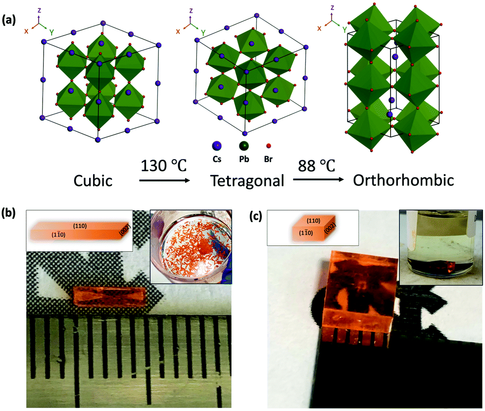 | ||
| Fig. 1 (a) CsPbBr3 structure at different temperature. The transition from cubic to tetragonal happens at 130 °C, and transition from tetragonal to orthorhombic happens at 88 °C. (b) Bar shape CsPbBr3 single crystal grown without CB. The left inset indicates the miller indices of each surface, and the right inset is the photograph of crystals in solution. (c) Cuboid shape CsPbBr3 single crystal grown with CB. The left inset indicates the miller indices of each surface, the right inset is the photograph of crystals in solution, and the bottom of the vial is a Si-wafer to make a flat bottom. | ||
Although we can control the crystal phase through growth temperature, the crystals grown from regular precursor solution (containing CsBr, PbBr2, and DMSO) still suffer from bar shape, which is in accordance with previous reports.39,50,51Fig. 1(b) presents the photo of a bar shape CsPbBr3 single crystal. The small bar shape makes it difficult to fabricate a practical detector. The bar shape mainly results from the asymmetric growth rate along different directions. To identify the various growth directions, we performed X-ray diffraction (XRD) and found the exposed facets to be (110), (1![[1 with combining macron]](https://www.rsc.org/images/entities/char_0031_0304.gif) 0), and (002), as shown in the left inset of Fig. 1(b and c). The crystal is elongated along [002] direction, which can be attributed to the fastest growth rate along this direction.
0), and (002), as shown in the left inset of Fig. 1(b and c). The crystal is elongated along [002] direction, which can be attributed to the fastest growth rate along this direction.
To investigate the reason that CsPbBr3 tends to grow faster along [002], we employed an attachment energy (AE) model developed by Hartman and Bennema, which has been widely used to predict crystal shape.52–54 The attachment energy of a facet (hkl) is defined as the released energy when a new layer of atoms is attached to the surface of the crystal. The energy is determined by the bonding strength and the number of bonds at a given face. Therefore, faces with a larger attachment energy have faster growth rates. Here, in CsPbBr3 orthorhombic structure, we mainly analyze (10) and (002) direction since the similarity in structure and growth rate of (110) and (10). Fig. 2(a) and (b) display the facets along [002] and [10], respectively. Two types of planes are presented normal to both directions. In particular, PbBr2 terminated (002) facet with Pb:Br ratio of 2:1 and CsBr terminated (004) facet with Cs:Br ratio of 1:1 are presented normal to [002] direction. CsBr terminated (10) facet with Cs:Br of 1:1, and PbBr2 terminated (2![[2 with combining macron]](https://www.rsc.org/images/entities/char_0032_0304.gif) 0) facet with Pb:Br of 2:1 are presented normal to [10] direction. Here we employed first principle calculations by using CASTEP program which has plane-wave pseudopotential method to calculate the AE of these four facets.55 The average AE of facets normal to the [002] direction was calculated to be 0.115 eV, 0.145 eV on (002) and 0.078 eV on (004). The average AE of the facets normal to [10] direction was calculated to be 0.095 eV, 0.084 eV on (10) and 0.110 eV on (20). The greater average AE calculated for facets along the [002] direction is congruent with the faster growth observed in the [002] direction of bar shaped crystals grown with no additives.
0) facet with Pb:Br of 2:1 are presented normal to [10] direction. Here we employed first principle calculations by using CASTEP program which has plane-wave pseudopotential method to calculate the AE of these four facets.55 The average AE of facets normal to the [002] direction was calculated to be 0.115 eV, 0.145 eV on (002) and 0.078 eV on (004). The average AE of the facets normal to [10] direction was calculated to be 0.095 eV, 0.084 eV on (10) and 0.110 eV on (20). The greater average AE calculated for facets along the [002] direction is congruent with the faster growth observed in the [002] direction of bar shaped crystals grown with no additives.
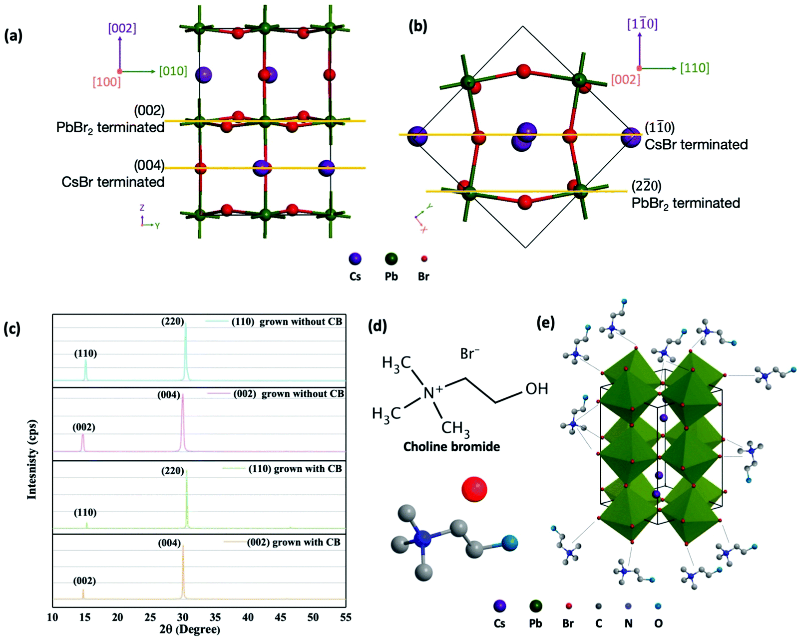 | ||
| Fig. 2 (a) Side view of the orthorhombic CsPbBr3 unit cell structure. The yellow lines indicate (002) and (004) plane. (b) Top view of the unit cell structure. The yellow lines indicate (10) and (20) plane. (c) XRD pattern of CsPbBr3 single crystal grown with and without CB. (d) Molecular structure of choline bromide (CB). (e) Schematic illustration of CB assisted CsPbBr3 single crystal growth. | ||
It is more favorable to have cuboid shape crystal to allow for easier fabrication and characterization of a detector. In this work, we found out that the addition of CB into precursor solution, containing CsBr, PbBr2, CB and DMSO, could alter the resulting shape of the CsPbBr3 crystals from a bar shape to a cuboid shape. As shown in Fig. 1(c), the cuboid crystal could maintain good transparency. The exposed facets were again characterized by XRD (Fig. 2(c)), and they all keep the same as the bar-shape crystal (left inset of Fig. 1(c)). Therefore, CB suppresses the [002] crystal growth rate without changing the CsPbBr3 structure. Here we propose a possible mechanism by which CB is capable of altering the anisotropic growth typically observed for CsPbBr3 single crystals. As shown in Fig. 2(d), CB is composed of quaternary ammonium group, a bromide ion, and a hydroxyl group. The positively charged quaternary ammonium group can coordinate with Br ions by electrostatic interactions, adsorb on the growing crystal, and subsequently block Cs+ or Pb2+ attaching on the crystal growth site, illustrated in Fig. 2(e). Therefore, the crystal growth rate was reduced from 1.25 mm3 h−1 in the solution without CB to 0.34 mm3 h−1 in the solution with CB. It should be noted that it is possible for choline molecules to coordinate with not only the (002) surface but also the (110)/(10) surfaces, due to the equal plane density of Br ions. However, the change from cuboid shape to bar shape suggests growth of the [002] is more inhibited than [110]/[10]. Because of the attachment of CB on those facets, the absorbing energy difference between these facets disappears. Therefore, crystals lose the preferred crystal growth direction. Here we demonstrate the addition of CB additives can be utilized to alter crystal growth to control the resulting crystal shape and produce attractive cuboid CsPbBr3 solution processed single crystals.
We further investigated if additive-assisted method could improve the crystal quality. To understand how CB influences the defect density within the crystals, the trap density of states (tDOS) of CsPbBr3 single crystal grown with and without CB was measured by thermal admittance spectroscopy, and the result is shown in Fig. 3(a). The CB-assisted growth process proves capable of drastically reducing the defect density of resulting crystals by roughly two orders of magnitude at low level traps states and approximately one order of magnitude at deeper trap states. In order to best characterize the quality of the crystal bulk, both types of crystals without obvious macroscopic defects were chosen in this measurement. Also, the surface of crystals was polished by sandpaper and passivated by (C8H17NH3)2SO4 to eliminate any influence arising from differences at the surface.56 This confirms that the CB-assisted ITC process is highly advantageous for not only altering the shape of the crystals, but also growing high-quality single crystals with reduced defect density.
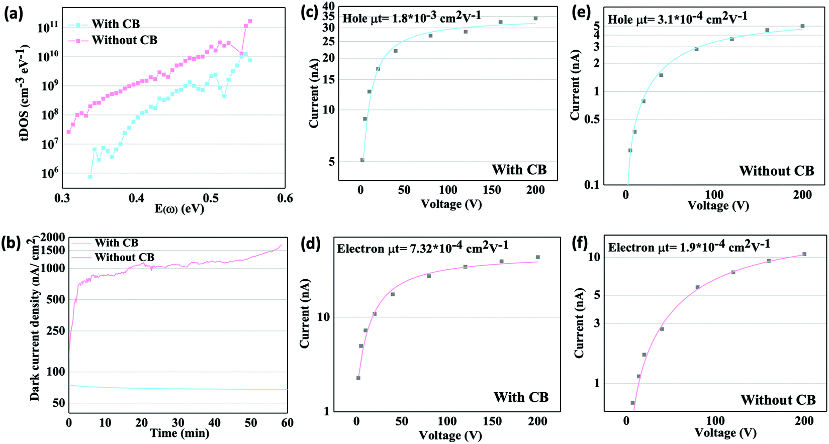 | ||
| Fig. 3 (a) tDOS and (b) dark current density as function of time of detectors with and without CB. (c) hole and (d) electron μτ product of detector with CB by Hecht equation fitting. (e) hole and (f) electron μτ product of detector without CB by Hecht equation fitting. | ||
It should be also noted that the concentration could impact the crystal defect density. Because the CB suppresses growth rate and decrease defect density by adsorbing on the surface of growing crystal. Small amount of CB could not offer enough quaternary ammonium groups if the size of the crystal is large. Therefore, we found obvious macroscopic defects at the edge of crystal due to the insufficient CB. In this work, the concentration of CB was 0.09 mol L−1 CB, and typical size of crystal at this concentration is around 9 mm × 9 mm × 3 mm.
The improved quality of crystals grown using the CB-assisted ITC process is also evident in the resulting performance of the fabricated detectors. Detectors are fabricated by depositing electrodes, gold (Au) cathode and gallium (Ga) anode, at the center of the crystals to suppress the leakage current flowing at the side surface which could otherwise corrupt the signal, Fig. 4(a). It is important to note that due to CsPbBr3 being an intrinsically p-type material, Ga is chosen as the anode in order to decrease the dark current density under high electrical field by forming a Schottky contact at the Ga side under reverse bias.21
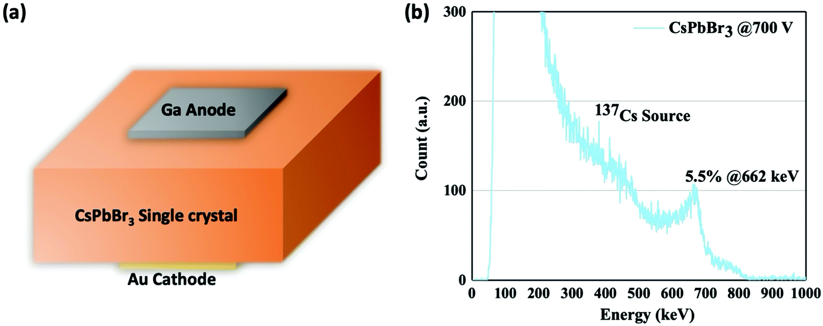 | ||
| Fig. 4 (a) Schematic of detector structure (4.5 mm × 4.5 mm electrode area, 2.5 mm thickness). (b) 662 keV 137Cs spectrum acquired by CsPbBr3 single crystal under 700 V. | ||
It is well reported that when under an electric field, ions within perovskite materials can migrate and result in a myriad of problems for all kinds of devices that need to be biased.57,58 The presence of point defects, lattice distortion, and dislocations within the bulk of single crystals can facilitate ion migration.59 Significant ion migration results in unstable dark current, known as dark current drift. Dark current drift can be particularly problematic for perovskite materials used in gamma-ray detection due to the extremely high applied voltage bias accelerating the ion migration process. Therefore, we can indirectly evaluate the crystal quality by assessing the dark current drift of the detectors. Detectors were biased under a large electric field of 910 V cm−1 and the dark current was recorded for one hour, as shown in Fig. 3(b). The dark current drift of detectors is effectively suppressed when using crystals grown using the CB-assisted method, resulting in a drift of only 6 nA cm−2 over one hour with a starting dark current of 74 nA cm−2. In contrast, the dark current density of the resulting detector without using the CB-assisted method started at 135 nA cm−2 and drifted to 1703 nA cm−2. The large dark current drift of the detector without CB is in consistent with the greater defect density shown in Fig. 3(a).
The mobility-lifetime (μτ) product is one of the important figures of merit for gamma-ray detectors. According to Hecht equation, the mobility-lifetime is an intrinsic parameter of a material that determines the charge collection efficiency.60 In this work, we use a 20 keV X-ray source to measure photocurrent at various voltages. Due to the high atomic density of CsPbBr3, the mean free path of 20 keV X-rays is only ∼30 μm (Linear attenuation coefficient-Photon energy plot in ESI,† Fig. S4). This means that the carriers are mainly generated near the surface of the 2.5 mm thick crystal. The μτ product is obtained by fitting the photocurrent I to the modified Hecht equation:
 | (1) |
The high atomic density, low trap density, stable dark current, and large μτ product suggest that CB-assisted CsPbBr3 single crystal detectors have immense potential for gamma-ray spectroscopy. To this end, we tested gamma-ray spectral performance under exposure to a 137Cs source emitting 662 keV gamma-rays. For the measurement, the 137Cs source was placed on the Au cathode side of CsPbBr3 detector (4.5 mm × 4.5 mm electrode area, 2.5 mm thickness), which was connected to a Charge Sensitive Preamplifier (CAEN A1422) and a CAEN N6724 Digitizer with embedded Digital Pulse Processing firmware. The typical resolution acquired by the CB-assisted CsPbBr3 detector is 9–10%, while the best resolution acquired at room temperature is 5.5% (Fig. 4(b)) with bias of 2700 V cm−1 and collection time of 15 min. It should be noted that low purity grade raw materials directly purchased from vendor were used to grow the single crystal, which could potentially be a source of undesirable impurities in the final crystal. It is expected that the performance and resolution of the detector can be further improved if high purity raw materials are used.35 The elevated Compton plateau in Fig. 4(b) can be attributed to the small volume of the crystal, resulting in a large fraction of scattered photons likely escaping from the detector. Therefore, future work can be focused scaling the additive assisted ITC solution growth process to produce larger crystals.
In conclusion, we demonstrate that high quality CsPbBr3 single crystals can be synthesized by using our new additive-assisted ITC solution growth method. The addition of choline bromide into the precursor solution is able to mediate the crystallization process to suppress the fast growth along [002] direction, thus reforming the shape of the resulting crystal from bar to cuboid. CB-assisted grown CsPbBr3 single crystals also exhibit lower trap density, and superior dark current stability, indicative of a higher quality crystal compared to those grown without CB. The CB-assisted CsPbBr3 single crystal detector also demonstrates excellent charge transport capabilities. Estimated by Hecht equation, the electron and hole mobility-lifetime (μτ) products are 0.73 × 10⁻³ cm2 V−1 and 1.80 × 10⁻³ cm2 V−1, respectively. More importantly, the CB-assisted CsPbBr3 single crystal is able to deliver a 662 keV 137Cs spectrum with resolution of 5.5%, which is, to date, the highest resolution acquired by a solution grown perovskite detector.
Experimental section
Chemicals and reagents
Low purity PbBr2 (≥98%), CsBr (≥99.9%), dimethyl sulfoxide (DMSO, ≥99.9%) were purchased from Sigma-Aldrich. Choline Bromide (CB, ≥98%) was purchased from TCI America. All raw materials and solvent were not further purified before using.Preparation of precursor solution
Standard CsPbBr3 precursor solution was obtained by dissolving CsBr (4.8 mmol) and PbBr2 (9.6 mmol) with a molar ratio of 1:2 in 5.3 mL DMSO solution. Precursor solution with CB was obtained by further adding 0.5 mmol CB to the standard precursor solution. The precursor solutions were heated to 80 °C to accelerate the dissolution of the raw material. Transparent solutions could be obtained after 5–10 hours. Solutions were then filtered with a 0.2 μm pore size PTFE filter.
Growth of CsPbBr3 single crystal
Small CsPbBr3 seeds were first prepared with fresh supersaturated precursor solution at 85 °C. Small and transparent seeds were then picked and put on the bottom of the vials for large crystal growth. The temperature of the vials was set at 80 °C initially with an increasing rate of 1 °C h−1, and was eventually maintained at 85 °C. Vials were covered with glass slides to avoid fast evaporation of the DMSO. So the growth driving force is supersaturation achieved by slow evaporation of DMSO solvent. After 120–170 hours, a centimeter-sized single crystal was picked from the solution, followed by wiping the residue solution on the surface.Detector fabrication
The resulting orange CsPbBr3 crystals were fine polished with 14000 grit polishing paper by the polishing machine. The dust on the polished surface was removed by nitrogen flow and washed by Toluene. The surface of the crystals was then spin-coated by (C8H17NH3)2SO4 for 2500 rpm to convert perovskite into lead sulfate (PbSO4) passivation layer, which is insoluble in water and large band gap. More details of the passivation can be found in our previous work.56 One side of the crystals was deposited with gold (Au) with a thickness of 50 nm by thermal evaporation. The other side was applied with gallium (Ga).
Characterization
The X-ray diffraction (XRD) was characterized by Rigaku MiniFlex X-ray diffractometer. Steady-state PL measurement was performed on a Horiba iHR320 imaging spectrometer at 25 °C. The excitation source was a 325 nm pulse laser. Dark current was measured by a Keithley 2400 Source meter with a sampling rate of 500 ms per point. Trap density of states (tDOS) was measured by admittance spectroscopy method, the device was kept dark during the entire test. The test was performed by an Agilent E4980A Precision LCR Meter. The energy profile of tDOS was calculated from the equation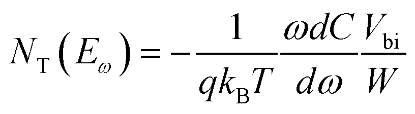 , where q is the elementary charge, ω is the angular frequency of the ac bias, C is the specific capacitance of the device, T is the temperature, kB is the Boltzmann constant, W is depletion width of the device, Vbi is the built-in potential. The energetic demarcation is derived by
 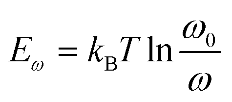 , where ω0 is the attempt-to-escape frequency. Mobility is obtained by the time-of-flight (ToF) technique. The excitation source was a 325 nm pulse laser. The photocurrent induced by laser was first fed into a SR-570 current pre-amplifie, and then recorded with an Agilent DSO-X 3104A digital oscilloscope. Mobility-lifetime (μτ) product was fitted from modified Hecht equation
 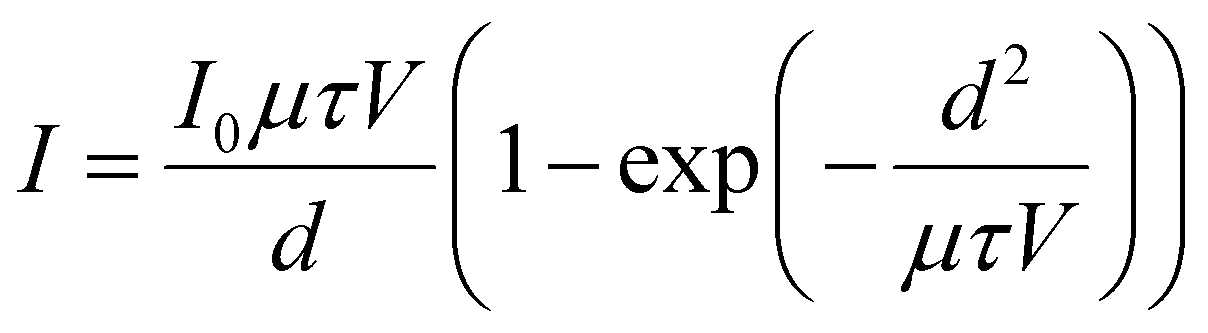 . The photocurrent is generated by a 20 keV X-ray beam. Sensitivity was measured under a different dose rate of 60 keV X-ray source. The radiation dose rate was calibrated by a RaySafe X2 dosimeter. Gamma-ray spectrum is collected by a Charge Sensitive Preamplifier (CAEN A1422), a CAEN N6724 Digitizer, and its embedded Digital Pulse Processing firmware.61
Conflicts of interest
There are no conflicts to declare.Acknowledgements
This research project is sponsored by the Department of the Defense, Defense Threat Reduction Agency under Grant HDTRA1170054. The content of the information does not necessarily reflect the position or the policy of the federal government, and no official endorsement should be inferred.References
- J. Hugg, B. Harris and H. Tomita, Evaluation of CZT gamma cameras for human SPECT and small FOV imaging, J. Nucl. Med., 2018, 59(suppl. 1), 220 Search PubMed.
- N. Gehrels, G. Chincarini, P. Giommi, K. O. Mason, J. A. Nousek, A. A. Wells, N. E. White, S. D. Barthelmy, D. N. Burrows, L. R. Cominsky, K. C. Hurley, F. E. Marshall, P. Meszaros, P. W. A. Roming, L. Angelini, L. M. Barbier, T. Belloni, S. Campana, P. A. Caraveo, M. M. Chester, O. Citterio, T. L. Cline, M. S. Cropper, J. R. Cummings, A. J. Dean, E. D. Feigelson, E. E. Fenimore, D. A. Frail, A. S. Fruchter, G. P. Garmire, K. Gendreau, G. Ghisellini, J. Greiner, J. E. Hill, S. D. Hunsberger, H. A. Krimm, S. R. Kulkarni, P. Kumar, F. Lebrun, N. M. Lloyd-Ronning, C. B. Markwardt, B. J. Mattson, R. F. Mushotzky, J. P. Norris, J. Osborne, B. Paczynski, D. M. Palmer, H. S. Park, A. M. Parsons, J. Paul, M. J. Rees, C. S. Reynolds, J. E. Rhoads, T. P. Sasseen, B. E. Schaefer, A. T. Short, A. P. Smale, I. A. Smith, L. Stella, G. Tagliaferri, T. Takahashi, M. Tashiro, L. K. Townsley, J. Tueller, M. J. L. Turner, M. Vietri, W. Voges, M. J. Ward, R. Willingale, F. M. Zerbi and W. W. Zhang, The Swift gamma-ray burst mission, Astrophys. J., 2004, 611(2), 1005–1020 CrossRef CAS.
- K. Iniewski, CZT detector technology for medical imaging, J. Instrum., 2014, 9, C11001 CrossRef.
- M. S. Pravikoff, C. Marquet and P. Hubert, Dating of wines with cesium-137: Fukushima's imprint, 2018, arXiv preprint arXiv:1807.04340.
- A. Tavendale, Large germanium lithium-drift pin diodes for gamma-ray spectroscopy, IEEE Trans. Nucl. Sci., 1965, 12(1), 255–264 CAS.
- P. Sangsingkeow, K. D. Berry, E. J. Dumas, T. W. Raudorf and T. A. Underwood, Advances in germanium detector technology, Nucl. Instrum. Methods Phys. Res., Sect. A, 2003, 505(1–2), 183–186 CrossRef CAS.
- R. Cooper, M. Amman and K. Vetter, High resolution gamma-ray spectroscopy at high count rates with a prototype high purity germanium detector, Nucl. Instrum. Methods Phys. Res., Sect. A, 2018, 886, 1–6 CrossRef CAS.
- J. F. Butler, S. J. Friesenhahn, C. L. Lingren, B. A. Apotovsky, F. P. Doty, W. L. Ashburn and W. P. Dillon, In Cd1−xZnx Te detector imaging array, Medical Imaging 1993: Physics of Medical Imaging, International Society for Optics and Photonics, 1993, pp. 30–38 Search PubMed.
- J. S. Iwanczyk, W. F. Schnepple and M. J. Masterson, The Effect of Charge Trapping on the Spectrometric Performance of Hgi2 Gamma-Ray Detectors, Nucl. Instrum. Methods Phys. Res., Sect. A, 1992, 322(3), 421–426 CrossRef.
- V. Deich and M. Roth, Improved performance lead iodide nuclear radiation detectors, Nucl. Instrum. Methods Phys. Res., Sect. A, 1996, 380(1-2), 169–172 CrossRef CAS.
- H. Malm, T. Raudorf, M. Martini and K. Zanio, Gamma ray efficiency comparisons for Si (Li), Ge, CdTe and HgI2 detectors, IEEE Trans. Nucl. Sci., 1973, 20(1), 500–509 CAS.
- L. Li, F. Lu, K. Shah, M. Squillante, L. Cirignano, W. Yao, R. W. Olson, P. Luke, Y. Nemirovsky, A. Burger, G. Wright and R. B. James, A new method for growing detector-grade cadmium zinc telluride crystals, 2001 Ieee Nuclear Science Symposium, Conference Records, 2002, vol. 1–4, pp. 2396–2400 Search PubMed.
- U. N. Roy, G. S. Camarda, Y. Cui, R. Gul, A. Hossain, G. Yang, J. Zazvorka, V. Dedic, J. Franc and R. B. James, Role of selenium addition to CdZnTe matrix for room-temperature radiation detector applications, Sci. Rep., 2019, 9, 1620 CrossRef CAS PubMed.
- A. E. Bolotnikov, G. S. Camarda, G. A. Carini, Y. Cui, K. T. Kohman, L. Li, M. B. Salomon and R. B. James, Performance-limiting defects in CdZnTe detectors, IEEE Trans. Nucl. Sci., 2007, 54(4), 821–827 CAS.
- A. E. Bolotnikov, S. Babalola, G. S. Camarda, Y. G. Cui, S. U. Egarievwe, R. Hawrami, A. Hossain, G. Yang and R. B. James, Te Inclusions in CZT Detectors: New Method for Correcting Their Adverse Effects, IEEE Trans. Nucl. Sci., 2010, 57(2), 910–919 CAS.
- J. K. Radhakrishnan, B. S. Sunderseshu, M. Srivastava, G. L. Seth, R. Raman, R. C. Narula and R. K. Bagai, Homogenization of zinc distribution in vertical Bridgman grown Cd(0.96)Zn(0.04)Te crystals, Bull. Mater. Sci., 2001, 24(6), 659–663 CrossRef CAS.
- N. Zhang, A. Yeckel, A. Burger, Y. L. Cui, K. G. Lynn and J. J. Derby, Anomalous segregation during electrodynamic gradient freeze growth of cadmium zinc telluride, J. Cryst. Growth, 2011, 325(1), 10–19 CrossRef CAS.
- A. Hossain, A. E. Bolotnikov, G. S. Camarda, Y. Cui, G. Yang and R. B. James, Defects in cadmium zinc telluride crystals revealed by etch-pit distributions, J. Cryst. Growth, 2008, 310(21), 4493–4498 CrossRef CAS.
- U. N. Roy, S. Weiler, J. Stein, Y. Cui, M. Groza, V. Buliga and A. Burger, Zinc mapping in THM grown detector grade CZT, J. Cryst. Growth, 2012, 347(1), 53–55 CrossRef CAS.
- S. U. Egarievwe, G. Yang, A. A. Egarievwe, I. O. Okwechime, J. Gray, Z. M. Hales, A. Hossain, G. S. Camarda, A. E. Bolotnikov and R. B. James, Post-growth annealing of Bridgman-grown CdZnTe and CdMnTe crystals for room-temperature nuclear radiation detectors, Nucl. Instrum. Methods Phys. Res., Sect. A, 2015, 784, 51–55 CrossRef CAS.
- Q. F. Dong, Y. J. Fang, Y. C. Shao, P. Mulligan, J. Qiu, L. Cao and J. S. Huang, Electron-hole diffusion lengths >175 μm in solution-grown CH3NH3PbI3 single crystals, Science, 2015, 347(6225), 967–970 CrossRef CAS PubMed.
- G. E. Eperon, S. D. Stranks, C. Menelaou, M. B. Johnston, L. M. Herz and H. J. Snaith, Formamidinium lead trihalide: a broadly tunable perovskite for efficient planar heterojunction solar cells, Energy Environ. Sci., 2014, 7(3), 982–988 RSC.
- D. Shi, V. Adinolfi, R. Comin, M. J. Yuan, E. Alarousu, A. Buin, Y. Chen, S. Hoogland, A. Rothenberger, K. Katsiev, Y. Losovyj, X. Zhang, P. A. Dowben, O. F. Mohammed, E. H. Sargent and O. M. Bakr, Low trap-state density and long carrier diffusion in organolead trihalide perovskite single crystals, Science, 2015, 347(6221), 519–522 CrossRef CAS PubMed.
- J. Kang and L. W. Wang, High Defect Tolerance in Lead Halide Perovskite CsPbBr3, J. Phys. Chem. Lett., 2017, 8(2), 489–493 CrossRef CAS PubMed.
- H. T. Wei and J. S. Huang, Halide lead perovskites for ionizing radiation detection, Nat. Commun., 2019, 10, 1066 CrossRef PubMed.
- S. Yakunin, D. N. Dirin, Y. Shynkarenko, V. Morad, I. Cherniukh, O. Nazarenko, D. Kreil, T. Nauser and M. V. Kovalenko, Detection of gamma photons using solution-grown single crystals of hybrid lead halide perovskites, Nat. Photonics, 2016, 10(9), 585–589 CrossRef CAS.
- Q. Wang, Y. C. Shao, H. P. Xie, L. Lyu, X. L. Liu, Y. L. Gao and J. S. Huang, Qualifying composition dependent p and n self-doping in CH3NH3PbI3, Appl. Phys. Lett., 2014, 105(16), 163508 CrossRef.
- H. T. Wei, D. DeSantis, W. Wei, Y. H. Deng, D. Y. Guo, T. J. Savenije, L. Cao and J. S. Huang, Dopant compensation in alloyed CH3NH3PbBr3−xClx perovskite single crystals for gamma-ray spectroscopy, Nat. Mater., 2017, 16(8), 826–833 CrossRef CAS PubMed.
- K. A. Bush, C. D. Bailie, Y. Chen, A. R. Bowring, W. Wang, W. Ma, T. Leijtens, F. Moghadam and M. D. McGehee, Thermal and Environmental Stability of Semi-Transparent Perovskite Solar Cells for Tandems Enabled by a Solution-Processed Nanoparticle Buffer Layer and Sputtered ITO Electrode, Adv. Mater., 2016, 28(20), 3937–3943 CrossRef CAS PubMed.
- S. N. Habisreutinger, T. Leijtens, G. E. Eperon, S. D. Stranks, R. J. Nicholas and H. J. Snaith, Carbon Nanotube/Polymer Composites as a Highly Stable Hole Collection Layer in Perovskite Solar Cells, Nano Lett., 2014, 14(10), 5561–5568 CrossRef CAS PubMed.
- C. C. Stoumpos, C. D. Malliakas, J. A. Peters, Z. F. Liu, M. Sebastian, J. Im, T. C. Chasapis, A. C. Wibowo, D. Y. Chung, A. J. Freeman, B. W. Wessels and M. G. Kanatzidis, Crystal Growth of the Perovskite Semiconductor CsPbBr3: A New Material for High-Energy Radiation Detection, Cryst. Growth Des., 2013, 13(7), 2722–2727 CrossRef CAS.
- P. Zhang, Q. H. Sun, Y. D. Xu, X. Li, L. Liu, G. D. Zhang and X. T. Tao, Enhancing Carrier Transport Properties of Melt-grown CsPbBr3 Single Crystals by Eliminating Inclusions, Cryst. Growth Des., 2020, 20(4), 2424–2431 CrossRef CAS.
- M. Z. Zhang, Z. P. Zheng, Q. Y. Fu, Z. Chen, J. L. He, S. Zhang, L. Yan, Y. X. Hu and W. Luo, Growth and characterization of all-inorganic lead halide perovskite semiconductor CsPbBr3 single crystals, CrystEngComm, 2017, 19(45), 6797–6803 RSC.
- J. Z. Song, Q. Z. Cui, J. H. Li, J. Y. Xu, Y. Wang, L. M. Xu, J. Xue, Y. H. Dong, T. Tian, H. D. Sun and H. B. Zeng, Ultralarge All-Inorganic Perovskite Bulk Single Crystal for High-Performance Visible-Infrared Dual-Modal Photodetectors, Adv. Opt. Mater., 2017, 5(12), 1700157 CrossRef.
- Y. H. He, L. Matei, H. J. Jung, K. M. McCall, M. Chen, C. C. Stoumpos, Z. F. Liu, J. A. Peters, D. Y. Chung, B. W. Wessels, M. R. Wasielewski, V. P. Dravid, A. Burger and M. G. Kanatzidis, High spectral resolution of gamma-rays at room temperature by perovskite CsPbBr3 single crystals, Nat. Commun., 2018, 9, 1609 CrossRef PubMed.
- J. X. Ding, S. J. Du, Z. Y. Zuo, Y. Zhao, H. Z. Cui and X. Y. Zhan, High Detectivity and Rapid Response in Perovskite CsPbBr3 Single-Crystal Photodetector, J. Phys. Chem. C, 2017, 121(9), 4917–4923 CrossRef CAS.
- M. I. Saidaminov, M. A. Haque, J. Almutlaq, S. Sarmah, X. H. Miao, R. Begum, A. A. Zhumekenov, I. Dursun, N. Cho, B. Murali, O. F. Mohammed, T. Wu and O. M. Bakr, Inorganic Lead Halide Perovskite Single Crystals: Phase-Selective Low-Temperature Growth, Carrier Transport Properties, and Self-Powered Photodetection, Adv. Opt. Mater., 2017, 5, 2 Search PubMed.
- Y. Rakita, N. Kedem, S. Gupta, A. Sadhanala, V. Kalchenko, M. L. Bohm, M. Kulbak, R. H. Friend, D. Cahen and G. Hodes, Low-Temperature Solution-Grown CsPbBr3 Single Crystals and Their Characterization, Cryst. Growth Des., 2016, 16(10), 5717–5725 CrossRef CAS.
- H. J. Zhang, X. Liu, J. P. Dong, H. Yu, C. Zhou, B. B. Zhang, Y. D. Xu and W. Q. Jie, Centimeter-Sized Inorganic Lead Halide Perovskite CsPbBr3 Crystals Grown by an Improved Solution Method, Cryst. Growth Des., 2017, 17(12), 6426–6431 CrossRef CAS.
- D. N. Dirin, I. Cherniukh, S. Yakunin, Y. Shynkarenko and M. V. Kovalenko, Solution-Grown CsPbBr3 Perovskite Single Crystals for Photon Detection, Chem. Mater., 2016, 28(23), 8470–8474 CrossRef CAS PubMed.
- F. B. Wang, H. J. Zhang, Q. H. Sun, A. Ben Hafsia, Z. X. Chen, B. B. Zhang, Y. D. Xu and W. Q. Jie, Low-Temperature Solution Growth and Characterization of Halogen (Cl, I)-Doped CsPbBr3 Crystals, Cryst. Growth Des., 2020, 20(3), 1638–1645 CrossRef CAS.
- H. J. Zhang, F. B. Wang, Y. F. Lu, Q. H. Sun, Y. D. Xu, B. B. Zhang, W. Q. Jie and M. G. Kanatzidis, High-sensitivity X-ray detectors based on solution-grown caesium lead bromide single crystals, J. Mater. Chem. C, 2020, 8(4), 1248–1256 RSC.
- M. I. Saidaminov, A. L. Abdelhady, B. Murali, E. Alarousu, V. M. Burlakov, W. Peng, I. Dursun, L. F. Wang, Y. He, G. Maculan, A. Goriely, T. Wu, O. F. Mohammed and O. M. Bakr, High-quality bulk hybrid perovskite single crystals within minutes by inverse temperature crystallization, Nat. Commun., 2015, 6, 7586 CrossRef PubMed.
- H. T. Wei, Y. J. Fang, P. Mulligan, W. Chuirazzi, H. H. Fang, C. C. Wang, B. R. Ecker, Y. L. Gao, M. A. Loi, L. Cao and J. S. Huang, Sensitive X-ray detectors made of methylammonium lead tribromide perovskite single crystals, Nat. Photonics, 2016, 10(5), 333–339 CrossRef CAS.
- M. I. Saidaminov, A. L. Abdelhady, G. Maculan and O. M. Bakr, Retrograde solubility of formamidinium and methylammonium lead halide perovskites enabling rapid single crystal growth, Chem. Commun., 2015, 51(100), 17658–17661 RSC.
- M. Liu, J. T. Zhao, Z. L. Luo, Z. H. Sun, N. Pan, H. Y. Ding and X. P. Wang, Unveiling Solvent-Related Effect on Phase Transformations in CsBr- PbBr2 System: Coordination and Ratio of Precursors, Chem. Mater., 2018, 30(17), 5846–5852 CrossRef CAS.
- S. Hirotsu, J. Harada, M. Iizumi and K. Gesi, Structural phase transitions in CsPbBr3, J. Phys. Soc. Jpn., 1974, 37(5), 1393–1398 CrossRef CAS.
- P. Cottingham and R. L. Brutchey, Depressed Phase Transitions and Thermally Persistent Local Distortions in CsPbBr3 Quantum Dots, Chem. Mater., 2018, 30(19), 6711–6716 CrossRef CAS.
- S. A. T. Redfern, High-temperature structural phase transitions in perovskite (CaTiO3), J. Phys.: Condens. Matter, 1996, 8(43), 8267–8275 CrossRef CAS.
- C. Y. Zhao, W. M. Tian, J. X. Li, Q. Sun, J. J. Luo, H. Yuan, B. D. Gai, J. Tang, J. W. Guo and S. Y. Jin, Stable Two-Photon Pumped Amplified Spontaneous Emission from Millimeter-Sized CsPbBr3 Single Crystals, J. Phys. Chem. Lett., 2019, 10(10), 2357–2362 CrossRef CAS PubMed.
- V. V. Belykh, D. R. Yakovlev, M. M. Glazov, P. S. Grigoryev, M. Hussain, J. Rautert, D. N. Dirin, M. V. Kovalenko and M. Bayer, Coherent spin dynamics of electrons and holes in CsPbBr3 perovskite crystals, Nat. Commun., 2019, 10, 673 CrossRef CAS PubMed.
- P. Hartman and P. Bennema, The attachment energy as a habit controlling factor: I. Theoretical considerations, J. Cryst. Growth, 1980, 49(1), 145–156 CrossRef CAS.
- J. J. Li, C. J. Tilbury, S. H. Kim and M. F. Doherty, A design aid for crystal growth engineering, Prog. Mater. Sci., 2016, 82, 1–38 CrossRef CAS.
- D. S. Coombes, C. R. A. Catlow, J. D. Gale, A. L. Rohl and S. L. Price, Calculation of attachment energies and relative volume growth rates as an aid to polymorph prediction, Cryst. Growth Des., 2005, 5(3), 879–885 CrossRef CAS.
- S. J. Clark, M. D. Segall, C. J. Pickard, P. J. Hasnip, M. I. Probert, K. Refson and M. C. Payne, First principles methods using CASTEP, Z. Kristallogr. – Cryst. Mater., 2005, 220(5/6), 567–570 CAS.
- S. Yang, S. S. Chen, E. Mosconi, Y. J. Fang, X. Xiao, C. C. Wang, Y. Zhou, Z. H. Yu, J. J. Zhao, Y. L. Gao, F. De Angelis and J. S. Huang, Stabilizing halide perovskite surfaces for solar cell operation with wide-bandgap lead oxysalts, Science, 2019, 365(6452), 473–478 CrossRef CAS PubMed.
- B. Chen, P. N. Rudd, S. Yang, Y. B. Yuan and J. S. Huang, Imperfections and their passivation in halide perovskite solar cells, Chem. Soc. Rev., 2019, 48(14), 3842–3867 RSC.
- Y. B. Yuan and J. S. Huang, Ion Migration in Organometal Trihalide Perovskite and Its Impact on Photovoltaic Efficiency and Stability, Acc. Chem. Res., 2016, 49(2), 286–293 CrossRef CAS PubMed.
- Y. Yuan and J. Huang, Ion migration in organometal trihalide perovskite and its impact on photovoltaic efficiency and stability, Acc. Chem. Res., 2016, 49(2), 286–293 CrossRef CAS PubMed.
- K. Hecht, Zum Mechanismus des lichtelektrischen Primärstromes in isolierenden Kristallen, Z. Phys., 1932, 77(3-4), 235–245 CrossRef CAS.
- L. Pan, Y. X. Feng, P. Kandlakunta, J. S. Huang and L. R. Cao, Performance of Perovskite CsPbBr3 Single Crystal Detector for Gamma-Ray Detection, IEEE Trans. Nucl. Sci., 2020, 67(2), 443–449 CAS.
Footnote |
| † Electronic supplementary information (ESI) available. See DOI: 10.1039/d0tc02706e |
| This journal is © The Royal Society of Chemistry 2020 |