
 Open Access Article
 This Open Access Article is licensed under a
 Creative Commons Attribution 3.0 Unported Licence
Atomic layer deposition of vanadium oxides for thin-film lithium-ion battery applications†
Felix Mattelaer *,
Kobe Geryl,
Geert Rampelberg,
Thomas Dobbelaere,
Jolien Dendooven and
Christophe Detavernier
*,
Kobe Geryl,
Geert Rampelberg,
Thomas Dobbelaere,
Jolien Dendooven and
Christophe Detavernier
Department of Solid State Sciences, Ghent University, Krijgslaan 281 S1, 9000 Gent, Belgium. E-mail: felix.mattelaer@ugent.be
First published on 8th December 2016
Abstract
Amorphous VO2 thin films are deposited by atomic layer deposition (ALD) using tetrakis[ethylmethylamino]vanadium (TEMAV) as vanadium precursor and water or ozone as the oxygen source. The crystallisation and oxidation behaviour is investigated for different oxygen partial pressures between ambient air and 3.7 Pa, resulting in phase formation diagrams on SiO2, TiN and Pt substrates, demonstrating a series of stable vanadium oxide phases in the VO2–V2O5 series. Most of the obtained phases exhibit lithium intercalation behaviour in the 1.5–4.5 V vs. Li+/Li potential range, and demonstrate high volumetric capacities in the order of V2O5 < VO2 (B) < V6O13 < V3O7 < V4O9, with the latter at more than twice the capacity of the best commercial cathode materials.
1 Introduction
The development of an ‘internet of things’ requires both wireless sensor networks and autonomous microsystems.1,2 While the electronics, sensors and wireless communication systems abide Moore’s law, the energy storage devices lag behind.2,3 To advance from traditional secondary batteries to energy storage systems tuned for these micro-devices, all-solid state thin-film batteries can provide the answer.4 While the removal of a liquid component in an all-solid state battery provides a huge advancement in battery safety and bio-compatibility,5 the thin-film approach provides integrability to on-chip devices as well as improved charge–discharge kinetics.Due to the transition-metal nature of vanadium oxides and the high number of vanadium–oxygen ratio compositions, vanadium oxides are heavily investigated materials for applications such as catalysis,6 optical switching7 and thin-film batteries.8–17 Although V2O5 and VO2 (B) are the most investigated cathode materials in lithium ion battery research,8–17 all vanadium oxides in the Wadsley series (VnO2n+1) are related to one another18 and show promising electrochemical properties.19,20 Even though vanadium oxides have a high theoretical energy density, they suffer from poor charge–discharge kinetics due to their moderate electronic conductivity and intrinsically low ionic diffusion.21
Upon going from a typical thin-film battery (1 to 10 μm thick electrodes) to truly thin-film electrodes (10 to 100 nm), the resistance for electronic current drops by orders of magnitude, and interface intercalation dominates over the bulk diffusion.22 However, the thin-film nature of these batteries inherently leads to a low energy density. This problem can be overcome by depositing these thin-films on complex battery architectures leading to significant enhancements in effective surface area and thus in energy density per footprint area.23–27 Many deposition techniques have been used to deposit a variety of vanadium oxides such as PVD,28,29 sol–gel29 and CVD,30 however, only few techniques have the high step-coverage of atomic layer deposition (ALD) required to coat the high-aspect-ratio structures required in 3D thin-film batteries.31 Several ALD processes exist for vanadium oxides.7,32–38
In this work, we will investigate the formation of vanadium oxide thin films in the VO2–V2O5 series, based on the atomic layer deposition of amorphous VO2. We will show that we can obtain all vanadium oxide phases in the series by changing the post-deposition annealing conditions, and demonstrate electrochemical activity of different phases.
2 Experimental
The vanadium oxides were grown in an experimental high-vacuum ALD setup with a base pressure of 10−7 mbar with walls heated at 95 °C.31,38,39 The ALD process used here was characterised earlier by Rampelberg et al.7,34–36,40 and is based on tetrakis[ethylmethylamino]vanadium (V(NC2H5CH3)4, or TEMAV) in combination with H2O and ozone. The precursor was held in a stainless steel container at 70 °C with argon as a carrier gas. TEMAV and argon were pulsed at a pressure of 6 × 10⁻³ mbar. As reactant gases H2O and O3 were applied, pulsed at 7.5 × 10⁻³ mbar and 2 × 10⁻¹ mbar, respectively. The ozone was produced with an OzoneLab™ generator from a pure O2 gas flow, resulting in a minimal concentration of 150 μg ml−1. In between pulses, reaction products and remaining precursor or reactant gas were evacuated using a turbomolecular pump to a pressure of <2.0 × 10⁻⁶ mbar. The films were grown on silicon substrates covered with 100 nm thermal SiO2, 60 nm PVD TiN and 80 nm PVD Pt. Two thermal ALD processes were used here: the TEMAV–H2O process and the TEMAV–O3 process. To ensure similar conditions, both processes were performed at a substrate temperature of 150 °C with saturated process parameters, as determined by earlier experiments.7,36 Pulse times for the TEMAV precursor were 5 and 4 s in the water and ozone processes. Water and ozone pulse times were 5 s on the SiO2 substrate. The Pt substrate influenced the growth, as was also reported by Premkumar et al.,34 so higher ozone pulse times (8 s) were required to ensure uniform films. The growth rate for the water process was 0.67 Å per cycle. The growth rate for the ozone process was 1.05 Å per cycle, a higher value than reported by Rampelberg et al.,7 but still lower than the reported value by Premkumar et al.34X-Ray techniques were used to determine film thickness (X-ray reflectivity or XRR), crystallinity (X-ray diffraction or XRD) and film composition and oxidation state (X-ray photoelectron spectroscopy or XPS). XRR and XRD were performed in a Bruker D8 Discover using a copper X-ray source (Cu-Kα radiation at 0.154 nm) and a point detector (for XRR) or a linear detector (for XRD). To determine the film crystallinity during annealing in a controlled ambient, in situ XRD was performed using a linear detector and a controlled ambient/temperature system. XPS was performed using Al-Kα radiation (0.834 nm) under a take-off angle of 45° in a high-vacuum chamber (2 × 10⁻⁹ mbar). A resolution of 0.108 eV was obtained.
The film morphology was probed using a Bruker Dimension Edge atomic force microscope (AFM) and film rms roughnesses were determined from 1 μm × 1 μm AFM images.
Electrochemical measurements were performed in an Ar-filled glove box (O2 < 1 ppm, H2O < 1 ppm) with a Metrohm Autolab PGSTAT302 connected to a three-electrode setup. Electrical contact to the TiN or Pt current collector was made by contacting the side of the sample with silver paste to a Cu foil. Lithium ribbon (99.9%, Sigma Aldrich) was used as counter and reference electrodes, and 1 M LiClO4 in propylene carbonate (99%, io-li-tec) was used as Li+ electrolyte solution. Cyclic voltammetry (CV) measurements were performed at a 10 mV s−1 sweep rate between 1.5 and 4.5 V vs. Li+/Li, or relevant potential boundaries. Galvanostatic charge–discharge measurements were performed to examine the capacity and thin film kinetics at varying current densities.
3 Results and discussion
3.1 VOx thin film deposition by thermal ALD
First, the properties of the as-deposited amorphous films were investigated. The rms roughness of the as-deposited films on a Pt substrate, as measured by AFM, was 1.95 and 1.77 nm for the H2O- and O3-based films, respectively. The Pt substrate was also measured, and showed a roughness of 1.75 nm, so the deposition of a 10 nm film on the substrate barely increases the roughness, indicating smooth films. The surface morphology was investigated using SEM, and images are shown in Fig. 1 for both films on the Pt substrate. A very similar granular morphology is observed for both processes. These results imply that the choice of process barely influences the as-deposited film morphology and topology. | ||
| Fig. 1 Morphology of the as-deposited VOx films on the Pt substrate as measured by SEM, showing the H2O-based (left) and O3-based (right) ALD films. | ||
Next, the film composition was investigated using XPS. Since vanadium oxides are reported to be very sensitive to the preferential sputtering of oxygen during depth profiling with XPS, only the surface spectra are evaluated to determine the composition and the oxidation state.42 The measured spectra were calibrated to the O![[thin space (1/6-em)]](https://www.rsc.org/images/entities/char_2009.gif) 1s signals at 530.0 eV, since calibrating using the C1s peak is not ideal for vanadium oxides.41 As the V2p core level binding energy depends strongly on its oxidation state,7,42 fitting can be used to determine the oxidation state of the as-deposited films. Furthermore, the separation of the V2p3/2 peak from the O1s VOx-component at 530.0 eV was also used to compare the two as-deposited ALD films.42 Fig. 2 shows the results of this analysis, alongside a V2O5 reference, using the reported binding energies for the V2p components: 515.8 and 523.2 eV for the V2p3/2 and V2p1/2, and 517.2 and 524.5 eV for the V2p3/2 and V2p1/2 for the V4+ and V5+ components, respectively. Both as-deposited films clearly have vanadium in the 4+ oxidation state.
1s signals at 530.0 eV, since calibrating using the C1s peak is not ideal for vanadium oxides.41 As the V2p core level binding energy depends strongly on its oxidation state,7,42 fitting can be used to determine the oxidation state of the as-deposited films. Furthermore, the separation of the V2p3/2 peak from the O1s VOx-component at 530.0 eV was also used to compare the two as-deposited ALD films.42 Fig. 2 shows the results of this analysis, alongside a V2O5 reference, using the reported binding energies for the V2p components: 515.8 and 523.2 eV for the V2p3/2 and V2p1/2, and 517.2 and 524.5 eV for the V2p3/2 and V2p1/2 for the V4+ and V5+ components, respectively. Both as-deposited films clearly have vanadium in the 4+ oxidation state.
 | ||
| Fig. 2 XPS spectra for the VOx film surface: (a) a crystalline V2O5 reference film, (b) as-deposited film using the water-based ALD process and (c) as-deposited film using the ozone-based ALD process. The binding energies are referenced to O1s calibrated at 530.0 eV.41 | ||
Even though the morphology and oxidation state of the as-deposited films are shown to be quite similar, a difference in film density was found by evaluating the V XRF counts, normalised to the Si-substrate XRF counts to account for surface and distance factors. When these values are compared to the film thicknesses measured by XRR, it is clear from Fig. 3 that there is more vanadium per unit thickness in the H2O-deposited films than in the O3-deposited film, a direct proof that the films grown by utilizing the water process are denser when compared to those grown from the ozone process, as is consistent with XRR and XRF measurements performed in earlier work.
 | ||
| Fig. 3 Relation between the XRF vanadium counts (normalised to the Si signal) and the measured film thickness (XRR) for different film thicknesses for both processes. The higher values for the H2O-based ALD films indicate a higher VOx density for these films. The dashed lines are a guide to the eye to illustrate this. | ||
3.2 VOx crystallisation and oxidation state control for 2 ≤ x ≤ 2.5
The as-deposited films using the TEMAV ALD processes are found to be amorphous by XRD with vanadium in a 4+ oxidation state. By post-ALD annealing in ambients with carefully controlled oxygen partial pressures, vanadium oxides in the VnO2n+1 series could be reached. The crystallisation was monitored using in situ XRD and the oxidation states were in accordance to the crystal state, as was confirmed by XPS on selected quenches (not shown here). Ex situ XRD on selected quenches confirmed the crystal states at intermediate temperatures. The crystallisation of the thin films was investigated on three substrates: SiO2, Pt and TiN.First, we will discuss the results on the SiO2 substrate. The systematic study of the crystallisation behaviour of the ALD VOx on the SiO2 substrate is presented in Fig. 4(a) and (b) for the H2O- and O3-ALD deposited films, respectively. As an example, the phase evolution of the ozone-grown film during annealing in a 3.7 Pa oxygen partial pressure is discussed here (top section of Fig. 4(b)). One can observe that the film is initially amorphous by the lack of diffraction peaks. When heating in a controlled ambient, the film crystallises into VO2 (B) just above 400 °C, and finally oxidizes between 500 and 600 °C to V6O13.
 | ||
| Fig. 4 Crystallisation of the as-deposited VOx thin films on the SiO2 substrate, as studied by in situ XRD in varying oxygen partial pressure at a heating rate of 0.25 °C s−1. Symbols indicate VOx crystal states (2 ≤ x ≤ 2.5), as shown in the legend (top left). | ||
The results of the in situ XRD measurements are summarized in ‘phase formation diagrams’, as shown in Fig. 5 for the crystallisation and oxidation on a SiO2 substrate. These should not be interpreted as thermodynamic phase diagrams, since no constant-temperature steps were made to allow film stabilisation to the equilibrium state, but as phase formation diagrams displaying the kinetic path the films go through while being heated at 0.25 °C s−1 in the ambients under study (He with oxygen partial pressure of 3.7, 7.4, 14.8, 29.6 and 48.1 Pa, and ambient air).
 | ||
| Fig. 5 Phase formation diagrams for the formation of crystalline VOx phases (2 ≤ x ≤ 2.5), based on the in situ XRD measurements (Fig. 4) at 0.25 °C s−1 for He ambients with oxygen partial pressures of 3.7, 7.4, 14.8, 29.6 and 48.1 Pa, and in ambient air. The same set of symbols is used as in Fig. 4 except for the extrema, namely VO2 and V2O5 states, since these dominate the phase formation diagrams to a large extent. | ||
The in situ XRD data provides a wealth of information on the often quite complex phase formation sequence. On SiO2 substrates, phase-pure regions were only observed for the VO2, V6O13 and V2O5 phases. A clear trend emerges when examining the influence of the oxygen partial pressure. When going through both formation diagrams in Fig. 5 from low to high oxygen partial pressure, we see that phases emerge and disappear in the order of increasing oxidation state: VO2–V6O13–V4O9–V3O7–V2O5 with respective average oxidation states for the V of 4–4.33–4.5–4.67–5. The influence of the temperature is more complex since the phases have no time to settle to an equilibrium state at each temperature, so thin-film kinetics will complicate this behaviour. However, we can see that in general with increasing temperature the average oxidation state rises to higher values, showing high-temperature stability for the higher oxides.
Furthermore, we can see the remarkable influence of the as-deposited film on the initial crystallisation of the amorphous layers. Since all parameters are equal except for the ALD process gas during the ALD process (ozone or water), this translates to an influence of the latter on the initial crystallisation. The ozone-based ALD crystallizes into the VO2 (B)-phase, while that via the water-based process crystallizes into the high-temperature stable (>68 °C) VO2 (R)-state (which settles to the VO2 (M1) state when quenched in that phase). Both these phases are based on a bcc lattice with vanadium on the octahedral sites. The difference lies in the mutual orientation of the fourfold axis of the oxygen octahedra, being aligned or perpendicular for the VO2 (B) and VO2 (R), respectively.43 This translates into a difference in structure as well as in density: VO2 (R) has a higher density (4.67 g cm−3) than VO2 (B) (4.03 g cm−3).44 Earlier, we showed that the water-based process leads to growth of a higher density amorphous VOx layer than the ozone process. The high density amorphous layer deposited using the H2O-based ALD process crystallizes into the high density VO2 (R) phase, while the lower density amorphous layer deposited using the ozone process crystallizes initially into the lower density VO2 (B) phase. So, by choice of ALD process, we can choose to crystallise the film in either the VO2 (B) or VO2 (M1) phase for electrochemical testing.
We hypothesize that the use of ozone in the ALD process also has an influence on the oxidation behaviour. Even though XPS shows that these films have the same oxidation state for the vanadium (4+), we observe a lower temperature for the introduction of higher oxidation state vanadium oxides for the ozone grown films. For the lowest oxygen partial pressure we obtain phase-pure VO2 for both films. For higher oxygen partial pressures, we see the presence of V4O9 upon crystallisation of the ozone grown films, having a higher oxidation state. For the water-grown films this was not the case, and we obtained phase-pure VO2 for all oxygen partial pressures examined (except for air), before further oxidation occurred. Even though the oxidation state is the same, a stronger oxidant is used during the ozone-based ALD process, which could incorporate more oxygen into the films. Another hypothesis is based on the fact that the films are less dense when using the ozone process. This could allow faster oxygen diffusion into these films, enhancing the oxidation kinetics during post-ALD annealing.
The crystallisation of the films on the Pt and TiN substrates was examined next, since a current collector is required to test the vanadium oxides as LIB electrode materials. The results are shown in Fig. 6. Similar trends were observed, with again formation of the VO2 (B) or VO2 (M1) as first phases for the ozone and water-based ALD, respectively, and the V2O5 phase occurring at high-temperature and/or high oxygen ambients. However, one can note two main differences when comparing these phase formation diagrams to those on SiO2. Firstly, the SiO2 formation diagrams are much richer in phase zones than their counterparts on Pt and TiN. Furthermore, we observed that on SiO2 the transformation to higher oxidation state vanadium oxides occurs at lower temperatures than on the other investigated substrates. In the case of a TiN substrate, the vanadium oxide phases with the highest oxidation states appear at the highest temperatures, or not at all, when compared to SiO2 and Pt. The Pt case lies in between both other cases. Here, we see the influence of the TiN in the substrate. We hypothesise that the TiN-substrate acts as an oxygen drain, extracting oxygen from the film, and thus preventing further oxidation of the vanadium oxides, as was also observed by the presence of TiO2 rutile diffraction peaks in the XRD scans taken after the oxidation experiments. The SiO2 is completely oxidized already, so it does not act as an oxygen drain, lowering the oxygen pressure and temperatures required to oxidise the vanadium oxides. The Pt substrate has a TiN layer underneath. Since oxygen can diffuse through the Pt layer, the underlying TiN can still get oxidized, as was confirmed by XRD. However, this oxidation is delayed by the presence of the Pt layer. This causes both observed differences: the phase-richness in the formation diagrams likely also occurs for TiN or Pt substrates, but at higher oxygen partial pressures than examined here, when the supply of oxygen is higher than the harvesting effect of the TiN.
 | ||
| Fig. 6 Phase formation diagrams for the formation of the VOx crystal states (2 ≤ x ≤ 2.5) on TiN substrates (left) and on Pt substrates (right), at 0.25 °C s−1 for He ambients with oxygen partial pressure of 3.7, 7.4, 14.8, 29.6 and 48.1 Pa, and in ambient air. The absence of the melt-line on the left figure is related to the presence of rutile TiO2 from the substrate, complicating the analysis of the VO2 (R) phase on the TiN substrate at high temperatures. | ||
3.3 Electrochemical characterisation of the possible VOx phases (2 ≤ x ≤ 2.5)
All of the obtained crystalline vanadium oxides (VO2 (B), VO2 (M1), V6O13, V4O9, V3O7 and V2O5) were tested as LIB electrodes on Pt substrates. Film crystallisation was monitored by in situ XRD to ensure corresponding phase formations and oxidations,† and results are summarised in Table 1. Only V3O7 was not obtainable in a phase-pure form on the Pt substrate, but the oxidation path indicated in Table 1 shows only a small fraction of the V3O7 film crystallised to V2O5, as was confirmed by XRD and XPS. This makes the V3O7 almost phase-pure, and will be denoted further simply as V3O7. The path to V6O13 does not match the phase formation diagram, since phase-pure V6O13 was obtained by performing a ramp slower than the one used for the formation diagrams. Cyclic voltammetry at 10 mV s−1 was performed down to 1.5 V vs. Li+/Li to examine the electrochemical intercalation behaviour of the different vanadium oxides. As can be seen in Fig. 7, all phases show a clear lithiation and delithiation behaviour. However, even though the VO2 (M1) appeared to show activity, initial galvanostatic charge–discharge tests showed only very low electrochemical storage capacity. Furthermore, some peaks of the cyclic voltammogram appear closely related to the electrochemical activity of the Pt substrate, as shown in ESI.† Due to the absence of storage of lithium into these films, VO2 (M1) was not examined in-depth further. All other films showed a clear lithium insertion/extraction behaviour, indicating lithium can be stored in these films reversibly.| Phase | ALD reactant | Ambient | Temperature (°C) |
|---|---|---|---|
| VO2 (B) | O3 | He + 3.7 Pa O2 | 420 |
| VO2 (M1) | H2O | He + 18 Pa O2 | 450 |
| V6O13 | O3 | He + 3.7 Pa O2 | 550 |
| V4O9 | H2O | Ambient air | 356 |
| V3O7 | O3 | He + 48 Pa O2 | 560 |
| V2O5 | H2O or O3 | Ambient air | 500 |
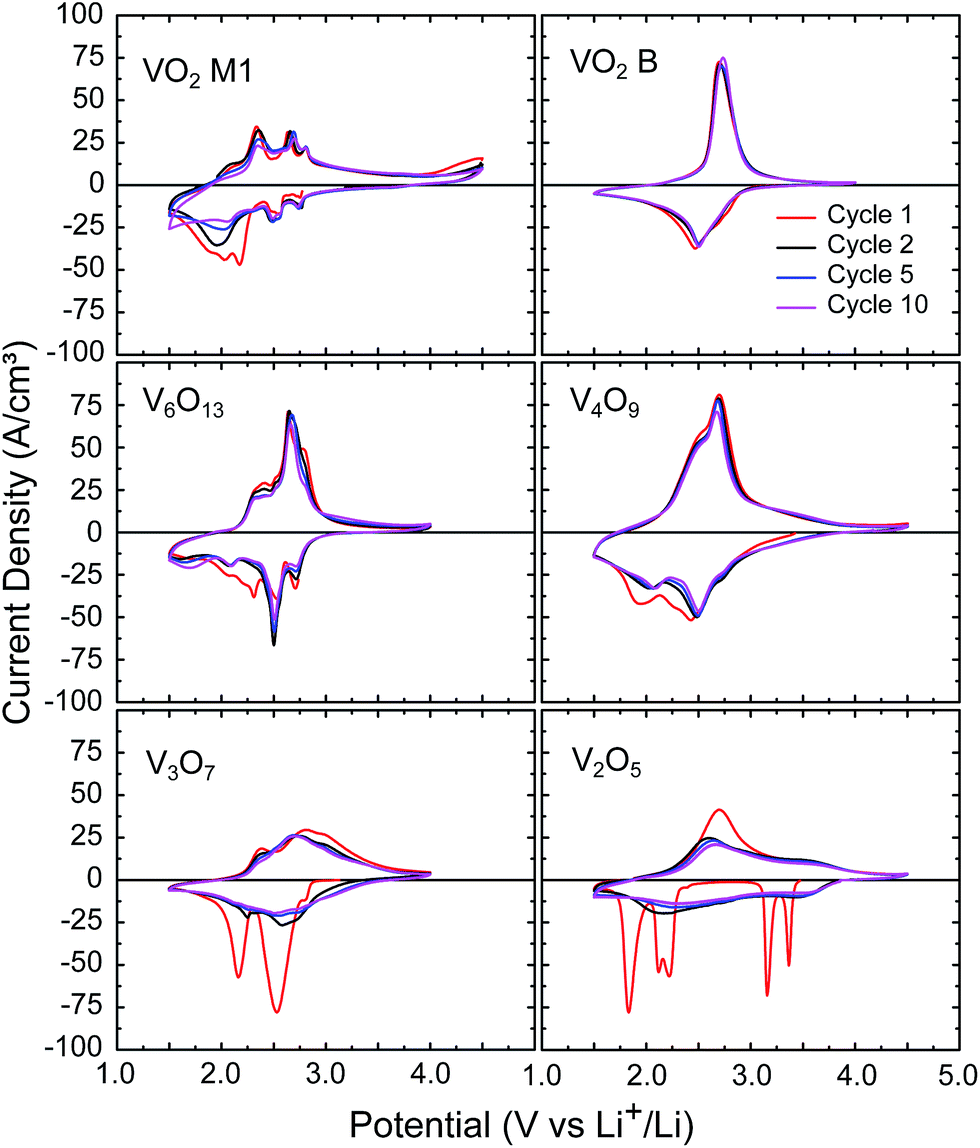 | ||
| Fig. 7 Cyclic voltammetry on the selected vanadium oxide thin films, performed at 10 mV s−1 in a three-electrode setup with lithium as counter and reference electrodes, and 1 M LiClO4 in PC as electrolyte. Potential ranges were chosen according to activity. | ||
Galvanostatic charging and discharging was performed on the films to determine the available storage capacity and compare it to V2O5, which is the most investigated form of vanadium oxide and is generally considered to be the most promising phase. The films were cycled at varying current densities between 0.1C and 100C, and the capacity was extrapolated to the 1C capacity to allow direct comparison between the different VOx phases, as shown in Fig. 8. Extrapolation was performed by fitting a linear relation to the logarithm of the capacity plotted to the logarithm of the C-rate, which provided fits with R2 > 0.98, demonstrating the validity of this approach. Table 2 summarizes the extrapolated capacities at 1C. Both Table 2 and Fig. 8 clearly demonstrate that, although V2O5 is the most investigated vanadium oxide for LIB cathodes, the capacity of the stable region (which corresponds to insertion of one lithium into V2O5), has a limited volumetric capacity. This is related to the low density of this V2O5 (3.36 g cm−3) compared to that of commercial lithium-ion cathodes such as LiCoO2 (4.9 g cm−3).45 All of the other investigated vanadium oxide phases have capacities well above the commercial cathodes, which is spearheaded by LiNi0.33Mn0.33Co0.33O2 (NMC) with a capacity of 600 mA h cm−3. The higher capacity for other vanadium oxides has an origin in increased material density and insertion range. First, the densities of the lower oxidation state vanadium oxides are higher than that of V2O5, leading to a higher volumetric capacity density; V3O7, V4O9, V6O13 and the VO2 (B) films have densities of 3.61, 3.78, 3.91 and 4.0 g cm−3, respectively. Second, while V2O5 can only be used in the narrow range that leads to LiV2O5, i.e. reduction of vanadium from V5+ to an average oxidation state of V4.5+, the vanadium in the series of vanadium oxides tested here changes its oxidation state much more, ranging from a change in average oxidation state of 0.62 for VO2 (B) to almost 1.2 for V4O9. So, while V2O5 and VO2 (B) are generally considered the most promising cathode materials, vanadium oxides in between them exhibit higher volumetric capacities.
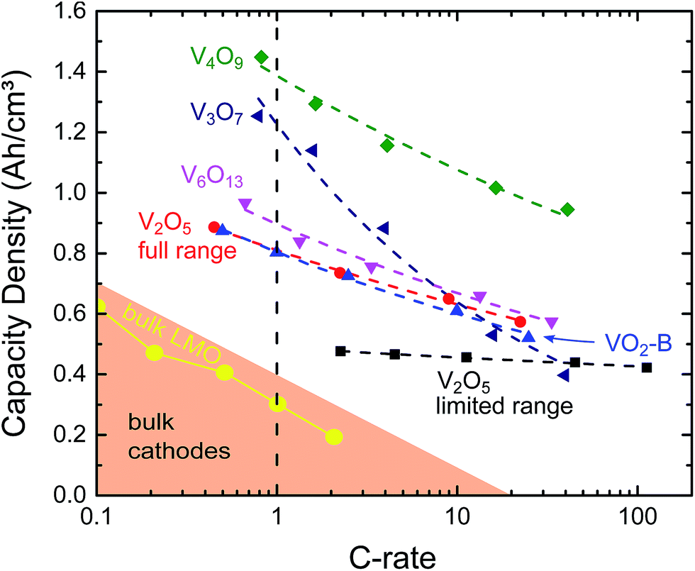 | ||
| Fig. 8 Measured delithiation capacity of the examined films on a logarithmic-linear scale (solid symbols). The data was extrapolated (dashed lines) resulting in a good match to the data (R2 > 0.98). Micron-sized LMO is shown as a model bulk cathode, (red circles)46 and more general bulk cathodes (shaded left corner)45 from literature are shown for comparison. | ||
| Potential (V vs. Li+/Li) | Volum. capacity (mA h cm−3) | |
|---|---|---|
| This work | ||
| VO2 (M1) | 1.5–4.0 | No activity |
| VO2 (B) | 1.5–4.0 | 805 (1C) |
| V6O13 | 1.5–4.0 | 894 (1C) |
| V4O9 | 1.5–4.0 | 1380 (1C) |
| V3O7 | 1.5–4.0 | 1255 (1C) |
| V2O5 (→LiV2O5) | 2.9–3.5 | 488 (1C) |
| V2O5 (→Li3V2O5) | 1.5–4.0 | 810 (1C) |
|
||
| Commercial cathode materials | ||
| LiCoO2 | 3.8 | 550 |
| LiMn2O4 | 4.1 | 596 |
| LiFePO4 | 3.4 | 589 |
| LiNi0.33Mn0.33Co0.33O2 | 3.7 | 600 |
| LiNi0.8Co0.15Al0.05O2 | 3.8 | 700 |
4 Conclusions
We demonstrated the deposition of two different forms of amorphous VO2 using two different ALD chemistries based on the same TEMAV precursor. Films were shown to be similar in morphology and as-deposited oxidation state of vanadium, but differ in density. By annealing these films in controlled ambients with varying oxygen partial pressures, we demonstrated that all crystalline phases between VO2 and V2O5 could be obtained. The substrate was found to influence the oxidation and crystallisation behaviour, with TiN acting as an oxygen drain delaying the oxidation. All obtained crystalline phases were characterised electrochemically, and showed activity as lithium-ion electrodes. We demonstrated that, while V2O5 is the most widely investigated vanadium-based cathode material, also VO2 (B), V6O13, V4O9 and V3O7 can be used as cathodes, with capacities up to 1380 mA h cm−3 (V4O9), more than twice the volumetric capacity for commercial cathode materials such as NMC.Acknowledgements
The authors acknowledge the IWT-Vlaanderen, BOF-UGent (GOA 01G01513), M-ERA LaminaLion, SBO SoS-Lion and the Hercules foundation for financial support. The authors also thank N. Deroo and Dr Ir. K. Devloo-Casier for the XPS measurements, and O. Janssens for assistance with the SEM and EDX measurements. J. D. and T. D. acknowledge the Flemish FWO for a postdoctoral and aspirant fellowship, respectively. Finally, the authors would like to thank the Air Liquide Advanced Materials team to provide us with the TEMAV precursor.References
- D. Miorandi, S. Sicari, F. De Pellegrini and I. Chlamtac, Ad Hoc Networks, 2012, 10, 1497–1516 CrossRef.
- H. Sundmaeker, P. Guillemin, P. Friess and S. Woelfflé, European Commission and Directorate-General for the Information Society and Media, Vision and challenges for realising the Internet of things, EUR-OP, Luxembourg, 2010 Search PubMed.
- A. S. M. Zahid Kausar, A. W. Reza, M. U. Saleh and H. Ramiah, Renewable Sustainable Energy Rev., 2014, 38, 973–989 CrossRef.
- M. Létiche, E. Eustache, J. Freixas, A. Demortière, V. De Andrade, L. Morgenroth, P. Tilmant, F. Vaurette, D. Troadec, P. Roussel, T. Brousse and C. Lethien, Adv. Energy Mater., 2016, 1601402 CrossRef.
- Y. Wang, W. D. Richards, S. P. Ong, L. J. Miara, J. C. Kim, Y. Mo and G. Ceder, Nat. Mater., 2015, 14, 1026–1031 CrossRef CAS PubMed.
- J. Keränen, A. Auroux, S. Ek and L. Niinistö, Appl. Catal., A, 2002, 228, 213–225 CrossRef.
- G. Rampelberg, M. Schaekers, K. Martens, Q. Xie, D. Deduytsche, B. De Schutter, N. Blasco, J. Kittl and C. Detavernier, Appl. Phys. Lett., 2011, 98, 162902 CrossRef.
- M. S. Whittingham, J. Electrochem. Soc., 1976, 123, 315–320 CrossRef CAS.
- D. W. Murphy, P. A. Christian, F. J. DiSalvo and J. V. Waszczak, Inorg. Chem., 1979, 18, 2800–2803 CrossRef CAS.
- P. G. Dickens, S. J. French, A. T. Hight and M. F. Pye, Mater. Res. Bull., 1979, 14, 1295–1299 CrossRef CAS.
- C. Delmas, H. Cognac-Auradou, J. M. Cocciantelli, M. Ménétrier and J. P. Doumerc, Solid State Ionics, 1994, 69, 257–264 CrossRef CAS.
- Y. Liu, M. Clark, Q. Zhang, D. Yu, D. Liu, J. Liu and G. Cao, Adv. Energy Mater., 2011, 1, 194–202 CrossRef CAS.
- C. Leger, S. Bach, P. Soudan and J.-P. Pereira-Ramos, J. Electrochem. Soc., 2005, 152, 236–241 CrossRef.
- Y. S. Cohen and D. Aurbach, Electrochem. Commun., 2004, 6, 536–542 CrossRef CAS.
- A. Pan, H. B. Wu, L. Yu, T. Zhu and X. W. D. Lou, ACS Appl. Mater. Interfaces, 2012, 4, 3874–3879 CAS.
- S.-L. Chou, J.-Z. Wang, J.-Z. Sun, D. Wexler, M. Forsyth, H.-K. Liu, D. R. MacFarlane and S.-X. Dou, Chem. Mater., 2008, 20, 7044–7051 CrossRef CAS.
- N. Ganganagappa and A. Siddaramanna, Mater. Charact., 2012, 68, 58–62 CrossRef CAS.
- H. A. Wriedt, Bull. Alloy Phase Diagrams, 1989, 10, 271–277 CrossRef CAS.
- M. S. Whittingham, Chem. Rev., 2004, 104, 4271–4302 CrossRef CAS PubMed.
- D. W. Murphy, P. A. Christian, F. J. DiSalvo and J. V. Waszczak, Inorg. Chem., 1979, 18, 2800–2803 CrossRef CAS.
- X. Huang, X. Rui, H. H. Hng and Q. Yan, Part. Part. Syst. Charact., 2015, 32, 276–294 CrossRef CAS.
- J. Jiang, Y. Li, J. Liu, X. Huang, C. Yuan and X. W. D. Lou, Adv. Mater., 2012, 24, 5166–5180 CrossRef CAS PubMed.
- J. F. M. Oudenhoven, L. Baggetto and P. H. L. Notten, Adv. Energy Mater., 2011, 1, 10–33 CrossRef CAS.
- Y. Wang and G. Cao, Adv. Mater., 2008, 20, 2251–2269 CrossRef CAS.
- L. Baggetto, R. A. H. Niessen, F. Roozeboom and P. H. L. Notten, Adv. Funct. Mater., 2008, 18, 1057–1066 CrossRef CAS.
- J. W. Long, B. Dunn, D. R. Rolison and H. S. White, Chem. Rev., 2004, 104, 4463–4492 CrossRef CAS PubMed.
- X. Meng, X.-Q. Yang and X. Sun, Adv. Mater., 2012, 24, 3589–3615 CrossRef CAS PubMed.
- J. Musil, P. Baroch, J. Vlček, K. Nam and J. Han, Thin Solid Films, 2005, 475, 208–218 CrossRef CAS.
- T. J. Hanlon, R. E. Walker, J. A. Coath and M. A. Richardson, Thin Solid Films, 2002, 405, 234–237 CrossRef CAS.
- N. Bahlawane and D. Lenoble, Chem. Vap. Deposition, 2014, 20, 299–311 CrossRef CAS.
- J. Dendooven, D. Deduytsche, J. Musschoot, R. L. Vanmeirhaeghe and C. Detavernier, J. Electrochem. Soc., 2010, 157, G111–G116 CrossRef CAS.
- J. C. Badot, S. Ribes, E. B. Yousfi, V. Vivier, J. P. Pereira-Ramos, N. Baffier and D. Lincot, Electrochem. Solid-State Lett., 2000, 3, 485–488 CrossRef CAS.
- P. Dagur, A. U. Mane and S. Shivashankar, J. Cryst. Growth, 2005, 275, 1223–1228 CrossRef.
- P. A. Premkumar, M. Toeller, I. P. Radu, C. Adelmann, M. Schaekers, J. Meersschaut, T. Conard and S. V. Elshocht, ECS J. Solid State Sci. Technol., 2012, 1, P169–P174 CrossRef CAS.
- T. Blanquart, J. Niinistö, M. Gavagnin, V. Longo, M. Heikkilä, E. Puukilainen, V. R. Pallem, C. Dussarrat, M. Ritala and M. Leskelä, RSC Adv., 2012, 3, 1179–1185 RSC.
- G. Rampelberg, D. Deduytsche, B. De Schutter, P. A. Premkumar, M. Toeller, M. Schaekers, K. Martens, I. Radu and C. Detavernier, Thin Solid Films, 2014, 550, 59–64 CrossRef CAS.
- M.-G. Willinger, G. Neri, E. Rauwel, A. Bonavita, G. Micali and N. Pinna, Nano Lett., 2008, 8, 4201–4204 CrossRef CAS PubMed.
- J. Musschoot, Q. Xie, D. Deduytsche, S. Van den Berghe, R. L. Van Meirhaeghe and C. Detavernier, Microelectron. Eng., 2009, 86, 72–77 CrossRef CAS.
- Q. Xie, Y.-L. Jiang, C. Detavernier, D. Deduytsche, R. L. V. Meirhaeghe, G.-P. Ru, B.-Z. Li and X.-P. Qu, J. Appl. Phys., 2007, 102, 083521 CrossRef.
- A. P. Peter, K. Martens, G. Rampelberg, M. Toeller, J. M. Ablett, J. Meersschaut, D. Cuypers, A. Franquet, C. Detavernier, J.-P. Rueff, M. Schaekers, S. Van Elshocht, M. Jurczak, C. Adelmann and I. P. Radu, Adv. Funct. Mater., 2015, 25, 679–686 CrossRef CAS.
- J. Mendialdua, R. Casanova and Y. Barbaux, J. Electron Spectrosc. Relat. Phenom., 1995, 71, 249–261 CrossRef CAS.
- G. Silversmit, D. Depla, H. Poelman, G. B. Marin and R. De Gryse, J. Electron Spectrosc. Relat. Phenom., 2004, 135, 167–175 CrossRef CAS.
- C. Leroux, G. Nihoul and G. Van Tendeloo, Phys. Rev. B: Condens. Matter Mater. Phys., 1998, 57, 5111–5121 CrossRef CAS.
- C. Leroux, G. Nihoul and G. Van Tendeloo, Phys. Rev. B: Condens. Matter Mater. Phys., 1998, 57, 5111–5121 CrossRef CAS.
- N. Nitta, F. Wu, J. T. Lee and G. Yushin, Mater. Today, 2015, 18, 252–264 CrossRef CAS.
- B. Ebin, V. Battaglia and S. Gërmen, Ceram. Int., 2014, 40, 7029–7035 CrossRef CAS.
Footnote |
| † Electronic supplementary information (ESI) available: In situ XRD during the formation of crystalline films for electrochemical testing, and cyclic voltammetry of the Pt substrate. See DOI: 10.1039/c6ra25742a |
| This journal is © The Royal Society of Chemistry 2016 |