DOI:
10.1039/C5RA20980C
(Paper)
RSC Adv., 2016,
6, 3480-3486
Electronic structure and optical properties of Fe-doped SnS2 from first-principle calculations
Received
10th October 2015
, Accepted 15th December 2015
First published on 18th December 2015
Abstract
The electronic structure and optical properties of Fe-doped SnS2 were investigated using first-principle calculations. The results suggest that Fe-doped SnS2 is a half-metal and its band gap decreases due to the Fe doping, which leads to a red shift in the absorption edges. The enhancement of the absorption efficiency in the low energy region is also observed. Furthermore, the absorption coefficient in the visible region increases monotonically with an increase in Fe doping concentration (0% ≤ x ≤ 12.5%), whereas the intensity of the additional peaks in the infrared region increases with small doping concentrations (less than x = 8.33%) and decreases with heavy doping.
1. Introduction
With the irresistible growing global demand for energy, solar energy has been paid a great deal of attention due to its abundant, clean and renewable characteristics. Photovoltaic devices are the most important way to make full use of solar energy. Among the current photovoltaic devices, the development and applications of first generation solar cells based on crystalline or amorphous silicon have been limited because of their high cost, complex fabrication process and low optical absorption coefficient.1,2 In addition, solar cells based on CdTe and CuInGaSe2 have not been widely used because they contain the low abundant and expensive elements, Te and In.3–5 To date, many efforts have been concentrated on the search for new photovoltaic absorber materials based on metal sulfides such as ZnS, CdS, FeS2, MoS2 and SnS2.6–11 In this study, our interest is concentrated on SnS2, which has the advantage of high chemical stabilization, nontoxicity, low cost and abundance. As an indirect gap semiconductor with a band gap value of ∼2.0 eV, SnS2 can absorb most of the ultraviolet light and a small amount of visible light. Moreover, SnS2 has a larger specific surface area than conventional materials due to its hexagonal layered crystalline structure. These excellent characteristics make SnS2 an intriguing material for application in optoelectronic devices.12–16
As is well known, the proportion of visible light in solar energy is around 45%, whereas ultraviolet light is only 5%.17 In addition, good solar cell absorbers should meet the criteria of an optimal band gap value of close to 1.5 eV and high optical absorption coefficient greater than 1.0 × 104 cm−1. Therefore, to achieve the goal of SnS2 as a photovoltaic absorber material, the biggest challenge is to appropriately narrow its optical band gap and reach a much higher absorption coefficient in the whole solar range. More recently, many studies have proven that impurities and defects indeed have a significant influence on optoelectronic properties such as strong absorption in the low energy region (including the visible and near-infrared light regions) and high-efficient photocatalytic activity in the visible-light region of SnS2 host materials.18–21 For example, Xia et al. found that Ti doping into SnS2 could narrow its band gap and improve its absorption coefficient in the visible-light region.22 Kiruthigaa et al. proved that Zn-doped SnS2 could be used as photocatalytic materials.23 In addition, V-doped SnS2 was investigated as a new intermediate band material to produce an absorption spectrum in the UV-Vis-NIR range.24,25 These studies suggest that the applications of SnS2 have a bright future in optoelectronic devices. However, the shortcomings of Ti and Zn doped SnS2 is that they cannot utilize sunlight in the infrared region. For V-doped SnS2, its photocatalytic efficiency appears to be lower than that of pure SnS2 when its photon energy is higher than the SnS2 band gap. Thus, to utilize sunlight more effectively, other elements should be considered for doping into SnS2 host materials.
As is well known, FeS2 has a band gap of 0.95 eV (ref. 26) and Fe has been successfully used to improve the optical properties of In2S3.27 Moreover, less study has been carried out on the electronic and optical properties of Fe-doped SnS2 until now. In this study, first-principle calculations based on density functional theory (DFT) were performed to systematically study the electronic and optical properties of Fe-doped SnS2 systems. Moreover, five different structure configurations corresponding to Fe doping concentrations of x = 0%, 5.56%, 6.25%, 8.33%, and 12.50% were adopted to explore the effect of Fe doping concentrations on the properties of SnS2. The obtained results show that Fe doping into SnS2 could lead to strong absorption in the full solar spectrum area due to the formation of impurity bands in the band gap, which is similar to the results of Fe-doped In2S3. However, there is a difference between them. The intensity of the emerging peaks in the infrared region increases monotonically with an increase in Fe doping concentrations for Fe-doped In2S3,27 while it increases with small doping concentrations (less than x = 8.33%) and decreases with heavy doping for Fe-doped SnS2. Theoretical studies on the electronic and optical properties of SnS2 host materials are significant for a deeper understanding of their photoelectric mechanisms and better applications of these photovoltaic absorber materials.
2. Methods and computational details
All calculations carried out using projector augment wave (PAW) pseudopotentials are based on the DFT method, as implemented in the Vienna ab initio Simulation Package (VASP).28 The generalized gradient approximation (GGA) with the Perdew–Burke–Ernzerhof (PBE) formula was adopted for the exchange–correlation potential plus the onsite Coulomb interaction, U, within the GGA.29 A cutoff energy of 400 eV was set for the plane wave expansion, with the total energy converging to lower than 5 × 10⁻⁶ eV per atom between two steps. Both cell and atoms were fully relaxed until the residual forces were less than 0.01 eV Å−1. The valence electron configurations Sn (4d105s25p2), Fe (3d64s2) and S (3s23p4) were considered in this study. A grid of 7 × 7 × 4 k-point was used for the unit cell. While for Fe-doped SnS2, four different configurations of SnS2 super cells were considered, which correspond to Fe doping concentrations of x = 5.56%, 6.25%, 8.33% and 12.50%. Moreover, Monkhorst–Pack k-point meshes of 3 × 3 × 2, 4 × 4 × 1, 4 × 4 × 2 and 4 × 4 × 3 were used for Brillouin zone sampling.30 Moreover, the van der Waals interaction was considered using Grimme's DFT-D2 method due to the characteristic of the layer-type lattice.31 Then, all the calculations on electronic and optical properties were performed on the basis of the optimized super cells.
3. Results and discussions
It is noteworthy that the method of GGA usually underestimates the band gap for the static correlation of common approximations and delocalization error.32 Therefore, for the sake of accurately describing the electronic structure of SnS2, it is necessary to use other methods to correct the band-gap value. Dudarev et al. proved that the method of determining the value of U in relation to a single ion could correct the error of GGA.33 Therefore, U = 1.7 eV and U = 9.0 eV were chosen for Fe-3d and Sn-4d electrons on the basis of calculating the band gap values of FeS2 and SnS2.26,34
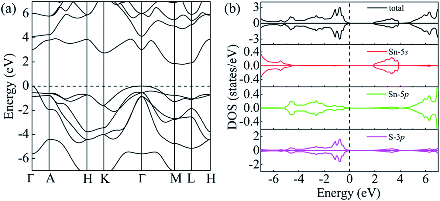
The optimized lattice parameters of pure SnS2 are a = 3.519 Å and c = 5.839 Å, which are in good agreement with experimental values (a = 3.649 Å and c = 5.899 Å).35 The calculated band structure and density of states (DOS) of pure SnS2 are shown in Fig. 1 as a reference. It can be observed from Fig. 1(a) that the valence band maximum (VBM) lies at the Γ point and the conduction band minimum (CBM) locates between the M and L points, which indicate that pure SnS2 is an indirect gap semiconductor. The calculated band gap is 1.81 eV, which is close to the experimental value of ∼2.00 eV.16 Moreover, as shown in Fig. 1(b), the conduction band is mainly dominated by the 5s and 5p orbitals of the Sn atom, and the 3p orbitals of the S atom. While the lower valence band from −7 to −5 eV mostly originates from the 5s orbitals of the Sn atom and the 3p orbitals of the S atom, and the upper valence band from −5 to 0 eV is derived from the 3p orbitals of the S atom and a little bit of 5p orbitals of the Sn atom. These properties have a good consistency with the previous results presented by Xia et al.,22 which suggests that the results of GGA + U method are reliable.
 |
| | Fig. 1 (a) Band structure and (b) DOS of unit SnS2. The Fermi level is set to 0. | |
To investigate the effect of Fe doping concentration on the electronic structure and determine the ideal band gap for photovoltaic absorber materials based on SnS2, the structural parameters and band gaps of Sn1−xFexS2 (x = 5.56%, 6.25%, 8.33%, and 12.50%) were calculated for the substitution of one Sn atom with Fe in four different configurations of SnS2 super cells. It can be observed from Table 1 that Fe doping leads to a decrease in the lattice parameters of SnS2, which may originate from the difference in bond length between Sn–S and Fe–S. The relaxed bond length of Fe–S is shorter than that of Sn–S. The reason for this is that the electronegativity difference between Fe and S atoms (0.75) is larger than that between Sn and S atoms (0.62). In addition, the CBM and VBM positions of the SnS2 systems are aligned with the core energy level of S-2s orbitals. For pure SnS2, the VBM position locates at the Fermi level. Based on the relative positions as compared with that of pure SnS2, the band gaps of doped SnS2 were obtained from the CBM and VBM positions presented in Fig. 2. Clearly, the band gap decreases monotonically with increasing Fe concentrations in the SnS2 host material, which implies that Fe doping can effectively modify the band gap of SnS2. One thing that should be noticed is that the change in the band gap trend is gradually gentle, especially at the doping concentrations of 8.33% to 12.50%.
Table 1 The lattice constants (a and c), and bond length between the Fe(Sn) atom and its nearest S atoms (dFe(Sn)–S) for pure SnS2 and Fe-doped SnS2
| Structural parameters (Å) |
0% |
5.56% |
6.25% |
8.33% |
12.50% |
| a |
3.519 |
3.508 |
3.507 |
3.505 |
3.498 |
| c |
5.839 |
5.795 |
5.793 |
5.618 |
5.781 |
| dFe(Sn)–S |
2.449 |
2.360 |
2.367 |
2.369 |
2.365 |
 |
| | Fig. 2 Band edge of Fe-doped SnS2 with different doping concentrations of x = 0%, 5.56%, 6.25%, 8.33% and 12.50%. | |
To specifically analyze the origin of the band gap narrowing of Fe-doped SnS2, Sn1−xFexS2 (x = 6.25%) was selected as the representative model. Moreover, the band structure, total density of states (TDOS) and partial density of states (PDOS) of Sn1−xFexS2 (x = 6.25%) were calculated and are illustrated in Fig. 3 and Fig. 4. Compared with undoped SnS2, the most notable characteristic of the band structure for Fe-doped SnS2 is that the Fermi level emerges into the valence band in the minority spin channel, whereas the majority spin channel shows an appreciable gap. This result demonstrates that the material is a half-metal. Moreover, as shown in Fig. 4, the 3p orbitals of the S atom are the most dominant from −6.00 to −0.21 eV in the valence band, whereas the 5s and 5p orbitals of the Sn atom mostly locate in the energy range from 1.45 to 3.80 eV and from 4.56 to 7.00 eV, respectively. It can be found that the impurity bands in the band gap are mainly composed of Fe 3d states, which are separated into seven bands. Two minority-spin bands with the highest energy form the bottom of the conduction band with Sn 5s states. Two minority-spin bands locate across the Fermi level, forming the top of the valence band with S 3p states and up-shift the VBM. In this situation, the energy difference between the VBM and CBM is 1.44 eV, which is smaller than the band gap value of pure SnS2 (1.81 eV). Thus, compared with pure SnS2, it requires less energy for electron transition from the occupied states to the unoccupied states, which means that the absorption edges of Fe-doped SnS2 may have a red shift. The last one minority-spin and two majority-spin bands are in the energy range between 0.54 and 1.24 eV, which can absorb the low-energy photons, and then extend the absorption of SnS2 into the infrared region. Detailed information on this will be discussed in the following sections.
 |
| | Fig. 3 Band structure of Fe-doped SnS2 for the doping concentration x = 6.25%, with (a) majority spin and (b) minority spin. The Fermi level is set to 0. | |
 |
| | Fig. 4 TDOS and PDOS of Fe-doped SnS2 for the doping concentration x = 6.25%. The Fermi level is set to 0. | |
As we all know, the optical properties of photovoltaic absorber materials are crucial for optoelectronic devices. The components of optical properties that correspond to parallel to the c axis (E//c) are discussed in the present study, due to the greatest incident optical absorption coefficient along this direction. Then, the effect of Fe doping on the optical properties of SnS2 is comprehensively studied in the following part, and the doping concentrations are varied from x = 0% to 12.50%.
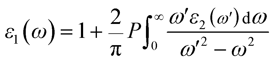
Based on the quantum theory, photons absorbed and emitted are the reasons for electron transitions between occupied and unoccupied states, including single-particle excitations and plasmons. Moreover, it should also be noted that the contribution from the two-band process has been proved strictly to be zero.36 It is necessary to calculate the dielectric function ε(ω) = ε1(ω) + iε2(ω) to completely characterize the optical properties of bulk materials based on SnS2.37 The imaginary part of the dielectric function ε2(ω) is not only related to the electronic structure of materials, but also presents the optical properties. It can be given as follows:38
| |
 | (1) |
where
i and
j are the initial and final states, respectively,
M is the dipole matrix, and
fi and
Ei are the Fermi distribution function and the energy of electron in
ith state, respectively. The real part of the dielectric function
ε1(
ω) can be evaluated from the imaginary part
ε2(
ω) with Kramers–Kronig transformation.
| |
 | (2) |
Then, other optical constants such as absorption coefficient α(ω), reflectivity R(ω), refractivity index n(ω) and energy-loss L(ω) can be obtained from ε1(ω) and ε2(ω).39
| |
 | (3) |
| |
 | (4) |
| |
 | (5) |
| | |
L(ω) = ε2(ω)/[ε12(ω)+ε22(ω)]
| (6) |
The imaginary part spectra of the dielectric function for Fe-doped SnS
2 with five different doping concentrations are presented in
Fig. 5(a). For pure SnS
2, we can observe two primary peaks. One locates at 3.88 eV, which originates from the electronic transition from the 3p orbitals of the S atom in the upper valence band to the 5s orbitals of the Sn atom in the lowest conduction band. The other locates at 7.32 eV, which originates from the electronic transition from the 3p orbitals of the S atom in the valence band to the 5p orbitals of the Sn atom in the conduction band. In the case of Fe-doped SnS
2 systems, the clear changes are that there appear new peaks in low energy region, indicating new and distinct channels for the absorption of photons with energies below the gap width of SnS
2 are obtained. The emerging peaks are at 0.29, 0.30, 0.29 and 0.42 eV for Fe doping concentrations of
x = 5.56%, 6.25%, 8.33% and 12.50%, respectively, which are due to the electronic intraband transition of the impurity Fe 3d states and the Sn 5s states in the conduction band. Moreover, the emerging peaks correspond to the localized degree of the impurity bands we discussed on the electronic properties above. Clearly, the intensity of the emerging peaks increases with small doping concentrations (less than
x = 8.33%) and decreases with heavy doping, which implies that there is a critical doping concentration for the strongest absorption in the infrared region. In addition, peaks similar to pure SnS
2 locate at around 3.59 to 4.08 eV and 7.19 to 7.27 eV. The former corresponds to the electronic transition from the S 3p states in the valence band to the Sn 5s states in the conduction band, whereas the later corresponds to the electronic transition from the S 3p states in the valence band to the Sn 5p states in the conduction band. What is noteworthy is that for the different structural configurations of SnS
2, the shape and the strength of the curves are nearly identical in the high energy region. These characteristics imply that different doping concentrations of Fe have a significant influence on the optical properties of SnS
2 systems in the low energy region, including visible and infrared region, whereas the effect is barely noticeable in the ultraviolet region, which demonstrates that Fe-doped SnS
2 systems are more suitable for long-wavelength optoelectronic devices compared with pure SnS
2.
 |
| | Fig. 5 (a) Imaginary part of the dielectric function and (b) absorption coefficient spectra of Sn1−xFexS2 (x = 0%, 5.56%, 6.25%, 8.33%, and 12.50%). The inset is an enlarged view of the infrared and visible light absorption spectra. | |
The absorption spectra of all the SnS2 systems are illustrated in Fig. 5(b). From the overall trend in the spectra we can observe that the absorption range is very wide, and the ultraviolet region is still the main absorption region. Compared with undoped SnS2, the absorption coefficient of Fe-doped SnS2 in visible region increases with an increase in Fe doping concentration, which is mainly induced by the enhancement of Fe 3d impurity states. Moreover, the additional absorption region is obtained in the infrared and visible region, which is below the absorption edges for Fe-doped SnS2 systems. This phenomenon is due to the electronic intraband transition of the impurity Fe 3d states and the Sn 5s states in the conduction band. Chen et al. found a similar phenomenon when they studied Fe-doped In2S3.27 Moreover, the emerging peaks in the low energy region improve the utilization efficiency of sunlight in the infrared region, which is consist with the above mentioned discussion on the imaginary part of the dielectric function. Furthermore, it can also be observed from Fig. 4 that the additional Fe 3d states in the band gap are the main reason that the peaks emerge in the low energy region. In addition, the absorption edges of the Fe-doped SnS2 systems monotonically shift to a lower energy with an increase in the Fe doping concentration, which is mainly the result of the decrease in the band gaps of the Fe-doped SnS2 systems. The red shift phenomenon is in accordance with the above mentioned analysis of electronic structure. Therefore, Fe doping will become a crucial factor that affects the optical properties of SnS2 and more notably, Fe-doped SnS2 shows more efficient utilization of solar energy compared with Ti, Zn and V-doped SnS2. In terms of optical absorption, compared with undoped SnS2, Fe-doped SnS2 can obtain a clear increase in the energy range of about 0 to 6.5 eV, whereas V, Ti and Zn-doped SnS2 enhance the absorption efficiency of the solar spectrum in energy of about 0 to 3.8 eV, 2.0 to 6.0 eV and more than 3.4 eV, respectively.22–24 According to the above mentioned discussion, it can be concluded that the Fe doping makes SnS2 a potential candidate for optoelectronic devices.
The reflectivity R(ω), refractivity index n(ω) and energy-loss L(ω) spectra of five different structure configurations of SnS2 systems are presented in Fig. 6. For Fe-doped SnS2, the reflectivity and refractivity index are greatly enhanced in the low energy region, which mainly originates from the impurity bands near the Fermi level. Moreover, both of them show the strongest peaks at around 0.2 eV and decrease abruptly in the low energy range between 0.2 and 1.2 eV. The location of the reflectivity and refractivity peaks also agree with the imaginary part spectrum of the dielectric function. Moreover, the energy-loss peaks at around 1.1 eV are related to the plasma oscillations wherein the reflectivity decreases rapidly. The above mentioned results indicate that the optical properties of Fe-doped SnS2 can become significantly improved in the low energy region, whereas this effect is less clear in the ultraviolet region.
 |
| | Fig. 6 Reflectivity, refractivity index, and energy-loss spectra of Sn1−xFexS2 (x = 0%, 5.56%, 6.25%, 8.33%, and 12.50%). | |
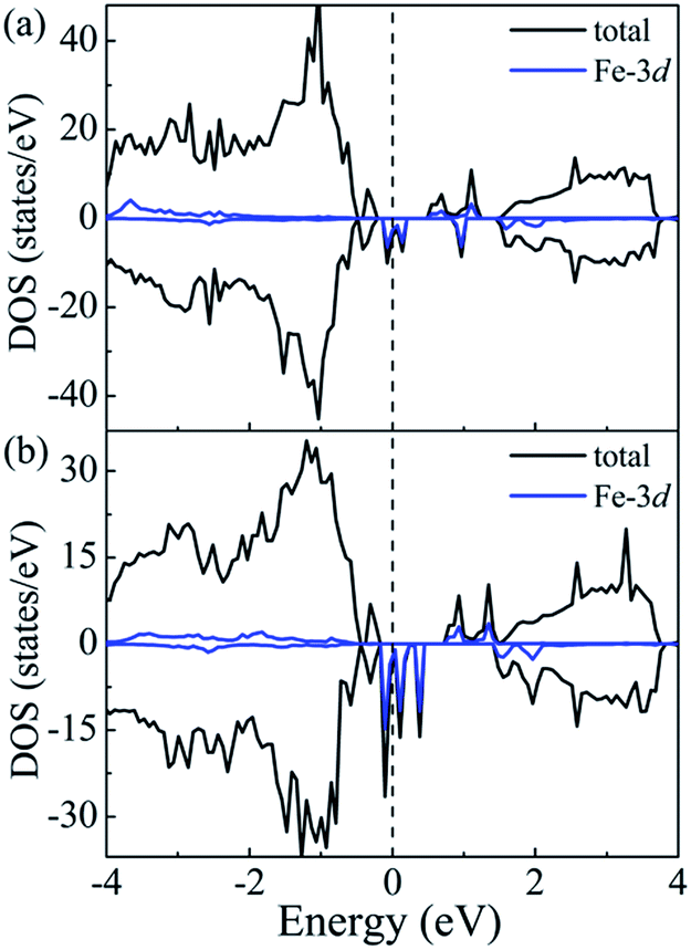
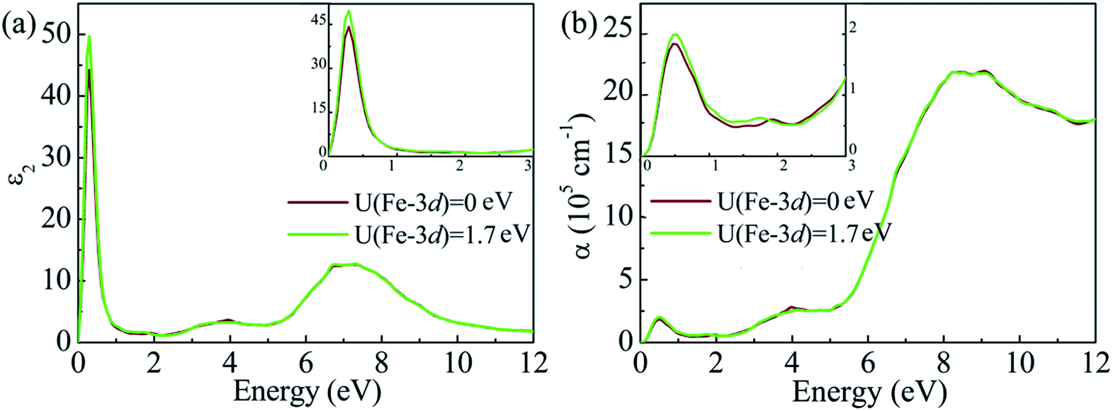
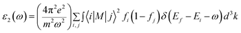
All the above mentioned results are obtained on the basis of the GGA + U method. It is generally known that the calculated band gap depends on the U value of the Hubbard model adopted in the calculations. Moreover, we have proven that the value of U adopted for Sn is in good agreement with the experimental band gap of pure SnS2. However, the gap of Fe-doped SnS2 may also rely on the U value for Fe. To explore the effect of the U value for Fe on the electronic and optical properties of Fe-doped SnS2, the doped bulk system Sn15Fe1S32 corresponding to a 6.25% doping concentration, is chosen as a reference. Moreover, the DOS, the imaginary part of the dielectric function and the absorption coefficient of Sn15Fe1S32 were calculated using the GGA + U method, where U = 9 eV for Sn-4d and U = 0 eV for Fe-3d are used. The results are presented in Fig. 7 and Fig. 8. The band gap obtained from Fig. 7(b) is 0.89 eV, which is considerably narrower than that of the doped system with the same structure corresponding to U = 9 eV for Sn-4d and U = 1.7 eV for Fe-3d. The reason for this is that the majority-spin intermediate states are lifted toward the CBM and then down-shift the CBM. It can be concluded from Fig. 7 that the effective Hubbard correction can lower the occupied majority spin states and increase the unoccupied minority spin states. The energy states of the intermediate states of Fe-doped SnS2 are largely determined by the U value for Fe, whereas the U value for Fe has little effect on the optical properties of Fe-doped SnS2. It can be observed from Fig. 8 that similar results are obtained with U = 0 eV and U = 1.7 eV for Fe-3d, which indicates that the results of the GGA + U (U = 9 eV for Sn-4d and U = 1.7 eV for Fe-3d) method can qualitatively reflect the properties of Fe-doped SnS2 systems.
 |
| | Fig. 7 Calculated DOS of Fe-doped SnS2 for the doping concentration x = 6.25% with the GGA + U method, where U = 9 eV for Sn-4d, (a) U = 1.7 eV and (b) U = 0 eV for Fe-3d are used. The Fermi level is set to 0. | |
 |
| | Fig. 8 (a) Calculated imaginary part of the dielectric function and (b) absorption coefficient spectra of Sn1−xFexS2 (x = 6.25%) with the GGA + U method, where U = 9 eV for Sn-4d, U = 1.7 eV and U = 0 eV for Fe-3d are used. The inset is an enlarged view of spectra in the infrared and visible region. | |
4. Conclusion
In conclusion, we have systematically studied the electronic structure and optical properties of Fe-doped SnS2 systems in five different structure configurations using the method of first-principle calculations. The electronic structures imply that Fe-doped SnS2 systems are half-metal due to the shift of the Fermi level from the VBM into the valence band. The band gap of Fe-doped SnS2 can be decreased from 1.81 to 1.44 eV when the Fe doping concentration is x = 6.25%. Moreover, the absorption edges of Fe-doped SnS2 systems show a red shift. The absorption coefficient in the visible region increases monotonically with an increase in Fe doping concentration. These characteristics indicate that the Fe-doped SnS2 system is a potential candidate for optoelectronic devices. In addition, the electronic intraband transition of the impurity Fe 3d states and the Sn 5s states in the conduction band broadens the sunlight absorption into the infrared region. The intensity of the emerging peaks in the infrared region increases with small doping concentrations (less than x = 8.33%) and decreases with heavy doping. Our calculations provide adequate evidence for effective utilization of solar energy, especially in the low energy region. These results not only contribute to the design of novel solar cells based on SnS2 hosts, but also promote further experimental studies.
Acknowledgements
This study was supported by the National Natural Science Foundation of China (51572190) and (11247224), and the super computing resources were supported by High Performance Computing Center of Tianjin University, China.
Notes and references
- M. Grätzel, Nature, 2001, 414, 338–344 CrossRef PubMed.
- D. E. Carlson and C. R. Wronski, Appl. Phys. Lett., 1976, 28, 671 CrossRef CAS.
- C. Candelise, M. Winskel and R. Gross, Prog. Photovoltaics, 2012, 20, 816 Search PubMed.
- M. A. Green, Prog. Photovoltaics, 2001, 9, 123 CAS.
- S. Lany and A. Zunger, Phys. Rev. B, 2005, 72, 035215 CrossRef.
- S. Kumar, M. Gradzielskic and S. K. Mehta, RSC Adv., 2013, 3, 2662–2676 RSC.
- Y. H. Huang, Z. Q. Zhang, F. Ma, P. K. Chu, C. P. Dong and X. M. Wei, Comput. Mater. Sci., 2015, 101, 1–7 CrossRef CAS.
- A. Kumar and P. K. Ahluwalia, Mater. Chem. Phys., 2012, 135, 755–761 CrossRef CAS.
- P. Lazić, R. Armiento, F. W. Herbert, R. Chakraborty, R. Sun, M. K. Y. Chan, K. Hartman, T. Buonassisi, B. Yildiz and G. Ceder, J. Phys.: Condens. Matter, 2013, 25, 465801 CrossRef PubMed.
- H. S. Lee, S.-W. Min, Y.-G. Chang, M. K. Park, T. Nam, H. Kim, J. H. Kim, S. Ryu and S. Im, Nano Lett., 2012, 12, 3695–3700 CrossRef CAS PubMed.
- R. J. Wei, J. C. Hu, T. F. Zhou, X. L. Zhou, J. X. Liu and J. L. Li, Acta Mater., 2014, 66, 163 CrossRef CAS.
- D. L. Greenaway and R. Nitsche, J. Phys. Chem. Solids, 1965, 26, 1445 CrossRef CAS.
- R. Bacewicz, B. Palosz, W. Palosz and S. Gierlotka, Solid State Commun., 1985, 54, 283 CrossRef CAS.
- H. X. Zhong, G. Z. Yang, H. W. Song, Q. Y. Liao, H. Cui, P. K. Shen and C. X. Wang, J. Phys. Chem. C, 2012, 116, 9319 CAS.
- Y. C. Zhang, Z. N. Du, S. Y. Li and M. Zhang, Appl. Catal., B, 2010, 95, 153–159 CrossRef CAS.
- L. A. Burton and A. Walsh, J. Phys. Chem. C, 2012, 116, 24262 CAS.
- J. L. Gole, J. D. Stout, C. Burda, Y. Lou and X. Chen, J. Phys. Chem. B, 2004, 108, 1230 CrossRef CAS.
- C. G. van de Walle and J. Neugebauer, J. Appl. Phys., 2004, 95, 3851 CrossRef CAS.
- R. Etefagh, N. Shahtahmasebi and M. Karimipour, Bull. Mater. Sci., 2013, 36, 411–416 CrossRef CAS.
- O. A. Yassin, A. A. Abdelaziz and A. Y. Jaber, Mater. Sci. Semicond. Process., 2015, 38, 81–86 CrossRef CAS.
- M. J. Powell, J. Phys. C: Solid State Phys., 1977, 10, 2967 CrossRef CAS.
- C. Xia, J. An, T. Wang, S. Wei and Y. Jia, Acta Mater., 2014, 72, 223–228 CrossRef CAS.
- G. Kiruthigaa, C. Manoharan, C. Raju, S. Dhanapandian and V. Thanikachalam, Mater. Sci. Semicond. Process., 2014, 26, 533–539 CrossRef CAS.
- P. Wahnon, J. C. Conesa, P. Palacios, R. Lucena, I. Aguilera, Y. Seminovski and F. Fresno, Phys. Chem. Chem. Phys., 2011, 13, 20401–20407 RSC.
- Y. Seminovski, P. Palacios and P. Wahnón, J. Phys.: Condens. Matter, 2014, 26, 395501 CrossRef PubMed.
- A. Rohrbach, J. Hafner and G. Kresse, J. Phys.: Condens. Matter, 2003, 15, 979 CrossRef CAS.
- P. Chen, H. Chen, M. Qin, C. Yang, W. Zhao and Y. Liu, J. Appl. Phys., 2013, 113, 213509 CrossRef.
- P. E. Blöchl, Phys. Rev. B, 1994, 50, 17953 CrossRef.
- J. P. Perdew, K. Burke and M. Ernzerhof, Phys. Rev. Lett., 1996, 77, 3865–3868 CrossRef CAS PubMed.
- H. J. Monkhorst and J. D. Pack, Phys. Rev. B, 1976, 13, 5188 CrossRef.
- S. J. Grimme, Comput. Chem., 2006, 85, 1787 CrossRef PubMed.
- A. J. Cohen, P. Mori-Sanchez and W. T. Yang, Chem. Rev., 2012, 112, 289 CrossRef CAS PubMed.
- S. L. Dudarev, G. A. Botton, S. Y. Savrasov, C. J. Humphreys and A. P. Sutton, Phys. Rev. B, 1998, 57, 1505 CrossRef CAS.
- C. X. Xia, Y. T. Peng, H. Zhang, T. X. Wang, S. Y. Wei and Y. Jia, Phys. Chem. Chem. Phys., 2014, 16, 19674 RSC.
- S. K. Arora, D. H. Patel and M. K. Agarwal, Cryst. Res. Technol., 1993, 28, 623 CrossRef CAS.
- B. B. Zhang, M. H. Lee, Z. H. Yang, Q. Jing, S. L. Pan, M. Zhang, H. P. Wu, X. Su and C. S. Li, Appl. Phys. Lett., 2015, 106, 031906 CrossRef.
- R. Chowdhury, S. Adhikari and P. Rees, Phys. B, 2010, 405, 4763 CrossRef CAS.
- C. M. I. Okoye, J. Phys.: Condens. Matter, 2003, 15, 5945 CrossRef CAS.
- L. Y. Li, W. H. Wang, H. Liu, X. D. Liu, Q. G. Song and S. W. Ren, J. Phys. Chem. C, 2009, 113, 8460–8464 CAS.
|
| This journal is © The Royal Society of Chemistry 2016 |
Click here to see how this site uses Cookies. View our privacy policy here.